EP4231661A1 - Mems device with a carrier structure comprising a plurality of angularly offset side face regions - Google Patents
Mems device with a carrier structure comprising a plurality of angularly offset side face regions Download PDFInfo
- Publication number
- EP4231661A1 EP4231661A1 EP22157894.1A EP22157894A EP4231661A1 EP 4231661 A1 EP4231661 A1 EP 4231661A1 EP 22157894 A EP22157894 A EP 22157894A EP 4231661 A1 EP4231661 A1 EP 4231661A1
- Authority
- EP
- European Patent Office
- Prior art keywords
- mems
- side face
- carrier structure
- mems device
- face region
- Prior art date
- Legal status (The legal status is an assumption and is not a legal conclusion. Google has not performed a legal analysis and makes no representation as to the accuracy of the status listed.)
- Pending
Links
Images











Classifications
-
- H—ELECTRICITY
- H04—ELECTRIC COMMUNICATION TECHNIQUE
- H04R—LOUDSPEAKERS, MICROPHONES, GRAMOPHONE PICK-UPS OR LIKE ACOUSTIC ELECTROMECHANICAL TRANSDUCERS; ELECTRIC HEARING AIDS; PUBLIC ADDRESS SYSTEMS
- H04R1/00—Details of transducers, loudspeakers or microphones
- H04R1/02—Casings; Cabinets ; Supports therefor; Mountings therein
- H04R1/04—Structural association of microphone with electric circuitry therefor
-
- H—ELECTRICITY
- H04—ELECTRIC COMMUNICATION TECHNIQUE
- H04R—LOUDSPEAKERS, MICROPHONES, GRAMOPHONE PICK-UPS OR LIKE ACOUSTIC ELECTROMECHANICAL TRANSDUCERS; ELECTRIC HEARING AIDS; PUBLIC ADDRESS SYSTEMS
- H04R2201/00—Details of transducers, loudspeakers or microphones covered by H04R1/00 but not provided for in any of its subgroups
- H04R2201/003—Mems transducers or their use
Definitions
- MEMS microelectromechanical system
- SNR signal-to-noise ratio
- MEMS microphones are limited partly by the size of sensitive elements.
- dimensions of a MEMS die may define capacitances in capacitive MEMS microphones.
- One approach to overcome this limit is an integration of multiple MEMS in one package.
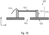
- Fig. 18 shows a schematic side view of a e.g. typical MEMS device (e.g., MEMS microphone).
- the MEMS device 1600 comprises a MEMS die 1610, e.g. a sound transducer, and a substrate 1620, e.g. a substrate of the package, wherein the MEMS die 1610 is attached to the substrate 1620.
- the MEMS die 1610 comprises a support structure 1612 and a membrane 1614 (e.g. + backplate, etc.) and an electrical contact 1616.
- the support structure 1612 is clamping or holding the membrane 1614 (+ further membranes and/or backplates e.g. in case of capacitive MEMS microphones).
- the substrate 1620 comprises a sound port 1622, e.g. an opening, for example of the packaged MEMS device.
- a package lid and an ASIC of device 1600 are not illustrated.
- the MEMS die 1610 may, for example, be integrated, e.g. directly, in the substrate 1620.
- Embodiments according to the disclosure comprise a MEMS device, the MEMS device comprising a MEMS die, and a carrier structure having an inner volume, wherein the carrier structure comprises a plurality of angularly offset side face regions for providing the inner volume.
- the MEMS die is mounted to a first side face region of the plurality of angularly offset side face regions and the MEMS die spans an opening in the first side face region.
- a second side face region of the plurality of angularly offset side face regions, different from the first side face region forms a basis portion for mechanically coupling the carrier structure to a substrate.
- a MEMS device comprising a carrier structure may allow to facilitate an integration of MEMS dies in the MEMS device, for example with only limited increase in required space, for example especially lateral space, e.g. parallel to a substrate of the MEMS device, e.g. a lateral space defining a footprint of the MEMS device.
- using a carrier structure according to embodiments may allow to achieve high signal-to-noise ratios, for example even in case of highly integrated MEMS devices with many MEMS dies.
- the carrier structure comprises an inner volume and a plurality of angularly offset side face regions for providing the inner volume.
- At least one MEMS die is mounted to a first side face region of the plurality of angularly offset side face regions, the MEMS die spanning an opening in the first side face region.
- the carrier structure e.g. a cubic carrier structure, for example an interposer device or an interposer structure
- the carrier structure may be a three-dimensional framework extending itself out of a substrate plane (e.g. in an assembled state of the MEMS device, wherein the MEMS device may, for example, be attached, or bonded to a substrate).
- additional, for example approximately or substantially perpendicular (e.g. to a substrate surface) carrier planes, in the form of the side face regions of the carrier structure, are provided, to which MEMS dies may be attached or mounted or bonded or glued.
- MEMS dies may be integrated three-dimensionally, e.g. out of a substrate plane, for example out of a plane parallel to a substrate of the MEMS device, or a plane of the MEMS device that may be parallel to a substrate surface in an assembled state.
- MEMS dies may be integrated in the MEMS device out of plane. This may allow usage of volumetric space of the MEMS device without increasing its footprint, for example significantly.
- the carrier structure may comprise openings in respective side face regions, to allow for an interaction of a respective MEMS die, e.g. in the form of a transducer, with an environment of the MEMS device (e.g. via the inner volume).
- the inner volume of the carrier structure may, for example, be coupled to an environment of the MEMS device via a port e.g. a sound port, e.g. in a substrate (e.g. coupled with the second side face region).
- the one or more openings in the side face regions may, for example, be holes through the carrier structure (e.g. wholly through a respective side face or side wall or side structure of the carrier structure).
- the one or more MEMS dies may share a common sound port.
- a plurality of MEMS dies spanning respective openings in respective side face regions may share one, e.g. single, sound port, for example for an interaction (e.g. signal detection or measurement) with a surrounding of the MEMS device.
- the MEMS device may be a, for example, high SNR, MEMS microphone with 3D integrated sensitive elements.
- the MEMS microphone may achieve a high SNR using an integration of a plurality of MEMS dies in the form of MEMS sound transducers using the carrier structure, e.g. such that the plurality of MEMS sound transducers is 3D integrated.
- embodiments may comprise a 3D integration of MEMS for high SNR microphones.
- a reference plane e.g. a main surface region of a substrate
- lateral means a direction parallel to the x- and/or y-direction or a direction parallel to (or in) the x-y-plane, wherein the term “vertical” means a direction parallel to the z-direction.
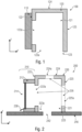
- Fig. 1 shows a schematic side view of a MEMS device according to embodiments of the present disclosure.
- Fig. 1 shows a MEMS device 100 comprising a MEMS die 110 and a carrier structure 120.
- the carrier structure comprises an inner volume 121 and a plurality of angularly offset side face regions 122, 123, 124, 125 for providing the inner volume 121.
- the MEMS die 110 is mounted to a first side face region 122 of the plurality of angularly offset side face regions. Furthermore, the MEMS die 110 spans an opening 122a in the first side face region.
- a second side face region 123 of the plurality of angularly offset side face regions, different from the first side face region, forms a basis portion for mechanically coupling the carrier structure to a substrate.
- the second side face region comprises an opening 123a to the inner volume 121 of the carrier structure, however it is to be noted that according to other embodiments of the disclosure such an opening 123a may not be present, the device 100 hence having a "closed" side face region 123, e.g. according to or analogously to or similar to the side face regions 124 or 125.
- the MEMS die may, for example, be in contact with an environment of the MEMS device 100, e.g. via the opening 123a.
- the inner volume 121 may, for example, be a closed volume.
- a MEMS die 110 may, for example be directly in contact with an environment of the MEMS device 100.
- the inner volume 121 may, for example, be a front volume or, e.g. in case opening 123a is not present a back volume.
- a device 100 may comprise a cubic carrier structure, for example as shown in Fig. 1 , or a pyramidal carrier structure, for example having less side face regions than shown in Fig. 1 .
- the carrier structure may, for example, be a polyhedron.
- the carrier structure may, for example, be a monolithic and/or integral carrier structure.
- the carrier structure may be made or fabricated from one piece.
- the carrier structure may be etched or manufactured from one workpiece, e.g. from a one-piece structure, e.g. in contrast to a carrier structure comprising a plurality of partial structures that were bonded or wielded or glued or soldered together or that were, for example, connected to each other with hinges and/or latches.
- the carrier structure may be produced with low effort, and for example with good mechanical properties, e.g. with good mechanical rigidity.
- the carrier structure may be an injection molded carrier structure and/or an additively manufactured carrier structure (e.g. a 3-D printed carrier structure).
- a main idea is the integration of MEMS dies 110 out of plane, for example, according to Fig. 1 out of the x-y plane, such that, in an assembled state, the MEMS die 110 is out of plane to a substrate.
- the MEMS die 110 may, for example, be substantially perpendicular to a substrate plane, e.g. the x-y plane, e.g. with a tolerance of less than 1° or of less than 5° or of less than 10° (e.g. measured to the y-z plane).
- device 100 may comprise a plurality of MEMS dies 110, attached to different side face regions of the device.
- the side face regions, having MEMS dies 110 attached to may comprise openings, e.g. analogously to side face region 122 with opening 122a.
- a footprint e.g. an area of the MEMS device 100 with respect to the x-y plane, may not be increased or may, for example, be increased only in a limited way, whilst providing a plurality of, e.g. out of plane, MEMS dies.
- MEMS device 100 being MEMS microphone
- MEMS dies 110 being MEMS sound transducers
- a high SNR with a e.g. very low footprint may be achieved.
- the second side face region 123 and the first side face region 122 may be non-parallel to each other.
- the second side face region 123 and the first side face region 122 may be non-parallel and adjacent to each other.
- MEMS die 110 may, for example, be attached to side face region 124 instead of side face region 122.
- a MEMS die can, for example, be arranged on top of the carrier structure, e.g. the cube.
- This side face region, e.g. 124 may, for example, be parallel, or substantially parallel, to the second, e.g. bottom side face region, e.g.
- second side face region e.g. the coupling side face region, and any side face region where a MEMS die or for example an ASIC die are provided, may be different planes or may, for example be in different planes.
- normal vectors of adjacent side face regions of the plurality of angularly offset side face regions may be non-parallel.
- a vector perpendicular to the y-z plane for the side face region 122 and a vector perpendicular to the x-y plane for the side face region 124 may be non-parallel.
- adjacent side face regions may comprise an angular offset, for example such that their respective normal vectors are non-parallel.
- Fig. 2 shows a schematic side view of a MEMS device with additional optional features, according to embodiments of the present disclosure.
- Fig. 2 shows a MEMS device 200 with at least one MEMS die 210, e.g. a sound transducer, and a carrier structure 220.
- the carrier structure 220 comprises a plurality of angularly offset side face regions 226, for providing an inner volume 221, as an example, the side face regions 222, 223, 224 and 225, wherein the MEMS die 210 is mounted or attached to a side face region 222, the side face region 222 comprising an opening 222a.
- a MEMS device 200 may comprise a plurality 226 of side face regions, e.g. faces, including or comprising at least one side face region 222 onto which a MEMS die 210 is provided.
- other side face regions e.g. side face region 223, side face region 224 and/or side face region 225 may comprise openings 223a, 224a and 225a respectively.
- one or even each other side face region e.g. apart from a second side face region 223 configured to be coupled with a substrate
- can be configured to optionally accommodate a further or another semiconductor chip e.g., additional MEMS dies and/or ASIC dies.
- one or more ASIC dies could be provided on a respective side face region of the structure, and/or on the substrate, the substrate for example being a package substrate, e.g. a substrate comprising packaged device 200.
- integrated circuitry e.g. in the form of an ASIC may be mounted to side face regions having no opening or to side face regions having an opening, e.g. besides a MEMS die spanning said opening.
- the MEMS die 210 comprises a support structure 212 (e.g. of the individual MEMS die 210) and a membrane 214 (e.g. comprising a backplate and/or further elements).
- the membrane 214 may, for example be an active part of the MEMS die 210 or the MEMS device 200.
- the MEMS device 200 comprises an electrical contact 230.
- the electrical contact may be configured to connect the MEMS die 210 with circuitry of the MEMS device 200 (not shown) or external circuitry, e.g. of a package comprising the MEMS device 200.
- the MEMS device 200 comprises a substrate 240, e.g. a carrier substrate.
- This substrate may as well be a substrate of a package, e.g. a package comprising the device 200.
- substrate 240 comprises a sound port 242, e.g. a common and/or shared sound port, e.g. a common or shared opening, for example, of the packaged MEMS device.
- Fig. 3a shows a schematic side view of a first MEMS device with optional features, according to embodiments of the present disclosure.
- MEMS device 300a comprises a carrier structure 320 having an inner volume 321 and angularly offset side face regions 322, 323, 324 and 325 for providing said inner volume 321.
- the first side face region 322 comprises an opening 322a and, as an optional feature, a further opening 322b.
- the MEMS device 300a comprises a MEMS die 310 that is mounted to the first side face region 322, spanning the opening 322a.
- device 300a comprises a further MEMS die 310a that is mounted to the first side face region 322 and that spans the further opening 322b.
- more than one MEMS die may be mounted or attached or bonded or glued to a respective side face region of the plurality of side face regions of the carrier structure. This may allow to further increase the packing density of MEMS dies in a MEMS device according to embodiments. It is to be noted, that to more than one side face regions, a plurality of MEMS dies may be mounted.
- MEMS die 310a may optionally span opening 322a.
- the second side face region 323 of the plurality of angularly offset side face regions forms a basis portion for mechanically coupling the carrier structure 320 to a substrate.
- side face region 323 comprises an opening 323a.
- the MEMS device 300a may comprise the substrate 340 and hence, the carrier structure 320 may be mechanically coupled or bonded or glued or attached to the substrate 340 via the second side face region 323.
- the MEMS device 300a comprises an additional MEMS die 310b, wherein the additional MEMS die 310b is mounted to the third side face region 324 of the plurality of angularly offset side face regions, and wherein the additional MEMS die 310b spans an opening 324a in the third side face region 324.
- the MEMS device 300a comprises an integrated circuitry 360, wherein the integrated circuitry is mounted to a side face region, as an example, as shown in Fig. 3a , to side face region 325, of the plurality of angularly offset side face regions.
- the integrated circuitry 360 is electrically coupled to the MEMS die 310 and/or any of the other MEMS dies 310a, 310b, and/or the integrated circuitry 360 may be configured to process at least one signal provided by the MEMS die 310 (and/or 310a, 310b) and/or the integrated circuitry 360 may be configured to provide a stimulus signal to the MEMS die 310 (and/or 310a, 310b).
- the substrate 340 comprises a sound port 342.
- the sound port may allow a coupling of the inner volume 321 with an environment of the MEMS device 300a.
- one of the MEMS dies 310, 310a 310b may, for example comprise a piezoelectric MEMS sound transducer and/or a capacitive MEMS sound transducer.
- an environmental influence e.g. a sound wave, may enter the inner volume 321 of the carrier structure 320 via the optional sound port 342, where it may be detected using at least one of the MEMS dies 310, 310a, 310b.
- At least of the MEMS dies 310, 310a 310b may comprise a sound transducer, an inertial sensor, a pressure sensor and/or a gas sensor.
- device 300a may comprise MEMS dies mounted to any of the side face regions that do not span an opening in the respective side face region.
- one of the MEMS dies 310, 310a or 310b may, for example, be an inertial sensor that may not require a contact with an environmental gas in order to provide a measurement.
- such a sensor may be mounted or attached to a side face region without spanning a respective opening.
- the MEMS device 300a further comprises a lid 350, wherein the lid 350 is mechanically coupled to the substrate.
- the lid may form an acoustically sealed back volume.
- the MEMS device 300a may, for example, be a MEMS microphone and the inner volume 321 of the carrier structure 320 may form a respective front volume of the MEMS microphone.
- Fig. 3a may show a bottom-port configuration of a MEMS microphone according to embodiments.
- An inventive structure according to Fig. 3a may allow to provide a big back volume in order to record a received acoustic signal with a good signal-to-noise ratio.
- Fig. 3b shows a schematic side view of a second MEMS device with optional features, according to embodiments of the present disclosure.
- MEMS device 300b comprises a substrate 340b without a sound port.
- lid 350b that may be mechanically coupled to the substrate 340b, comprises a sound port 352.
- the lid 350b coupled to the substrate 340b, may form a front volume, e.g. of the MEMS microphone.
- the inner volume 321b of the carrier structure 320 may form a back volume of the MEMS microphone.
- Fig. 3a may show a top-port configuration of a MEMS microphone according to embodiments.
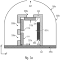
- Fig. 3c shows a schematic side view of a third MEMS device with optional features, according to embodiments of the present disclosure.
- the MEMS dies 310, 310a and 310b the integrated circuitry 360 are arranged in the inner volume 321c of the carrier structure 320.
- MEMS die 310 is mounted to a first side face region 326, spanning an opening 326a
- MEMS die 310a is mounted to the first side face region 326 as well, optionally spanning a further opening 326b in the first side face region
- MEMS die 310b is mounted to a third side face region 328 spanning a respective opening 328a.
- the integrated circuitry e.g. in general an ASIC, is mounted to a fourth side face region 329.
- a second side face region 327, optionally comprising an opening 327a, is coupled mechanically with substrate 340c.
- MEMS dies and/or integrated circuitry may be mounted to an inside of the carrier structure or to an outside of the carrier structure (e.g. as shown in Figs. 3a-c ). Hence any combination of the different attachments may be realized according to embodiments.
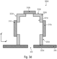
- Fig. 3d shows a schematic side view of a fourth MEMS device with optional features, according to embodiments of the present disclosure.
- MEMS device 300d comprises carrier structure 322d comprising a plurality of angularly offset side face regions 322d, 323d, 324d, 325d for providing the inner volume 321d.
- MEMS device 300d comprises a plurality of MEMS dies 310, 310c, wherein each MEMS die is mounted to a different side face region of the plurality of angularly offset side face regions.
- the side face regions 322d, 325d, to which the plurality of MEMS dies are mounted to are substantially perpendicular to the second side face region 323d.
- a MEMS dies 310b may as well be mounted to side face regions 324d substantially parallel to the second side face region 323d.
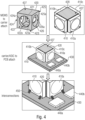
- Fig. 4 shows a schematic three-dimensional view of examples of manufacturing steps for a MEMS device according to embodiments of the disclosure.
- Fig. 4 may show an example for a main technical implementation of an embodiments according to the disclosure.
- a plurality of MEMS dies 410, 410a, 410b, 410c may be attached or mounted to a carrier structure 420 ("MEMS (die) to carrier (structure) attach").
- the carrier structure may comprise openings 422a, 423a, 424a, 425a, 426a in angular offset side face regions 422, 423, 424, 425, 426 providing an inner volume.
- the openings may have any geometrical shape suitable, e.g. as shown a round shape.
- a further side face region 427 may, for example be a top side face region.
- the MEMS dies 410, 410a, 410b, 410c may be mounted to respective side face regions 422, 424, 425, 426, such that they span a respective opening 422a, 424a, 425a, 426a.
- the carrier structure 420 may be attached or soldered or mounted to a substrate 430, e.g. a PCB (printed circuit board), for example, comprising integrated circuitry, e.g. as shown ASICs 440a, 440c ("Carrier/ASIC to PCB attach").
- a substrate 430 e.g. a PCB (printed circuit board)
- integrated circuitry e.g. as shown ASICs 440a, 440c ("Carrier/ASIC to PCB attach"
- the integrated circuitry may, for example, be attached to the substrate 430 after attaching the carrier structure 420 or vice versa.
- interconnections 450 e.g. electrical contacts, e.g. as explained in the context of Fig. 2 .
- the interconnections 450 may, for example, be configured to connect the MEMS dies 410, 410a, 410b, 410c to conductor tracks (not shown) of the substrate 430, that may, for example, be electrically coupled with integrated circuitry, e.g. with ASICs 440a, 440b.
- Fig. 5 shows a schematic three-dimensional view of an example for a MEMS device according to the manufacturing steps shown in Fig. 4 .
- MEMS device 500 comprises a lid 460.
- device 500 may comprise a plurality of MEMS dies and consequently the steps shown in Fig. 4 may allow an out of plane integration of 4+ (4 and more) MEMS chips (e.g. MEMS dies).
- MEMS dies can be attached to a carrier structure, e.g. carrier, to form a front volume, e.g. inner volume 421, acoustically isolated from a back volume, e.g. a volume arranged between the lid 460 and the substrate 430.
- devices with high or higher SNR may be provided, keeping a low or for example the same footprint and single sound port, e.g. as a single MEMS single sound port device.
- Fig. 6 shows a schematic view of a carrier structure design variant according to embodiments of the disclosure, e.g. a carrier design (main variant).
- Fig. 6 may show a main technical implementation for the carrier structure.
- Fig. 6 shows a schematic side view 610 of a carrier structure.
- the carrier structure may, for example, be a cubic carrier structure, e.g. with an edge length of, e.g. about, 1.8 mm (e.g. with a tolerance of +/-5% or with a tolerance of +/-20%, e.g.
- Openings in the side face regions of the carrier structure may, for example, be circular openings, e.g. comprising a diameter of, e.g. about, 1.3 mm (e.g. with a tolerance of +/-5% or with a tolerance of +/-20%, e.g.
- the openings may, for example be offset from an outer edge of the carrier structure by, e.g. about, 0.25 mm (e.g.
- the openings may, for example, be centered in a respective side face region. However it is to be noted that in general, openings in side face regions do not necessarily have to be centered.
- Schematic side view 620 shows a cross section through plane A-A of side view 610, highlighting an offset of the opening from an outer edge.
- Schematic three-dimensional views 630 and 640 show a carrier structure according to views 610 and 620 from different perspectives.
- Figs. 7 may show a main technical implementation according to embodiments of the disclosure, e.g. for a 90 degree wire bonding.
- a wire may be bonded to a MEMS die (or respectively a substrate) of a MEMS device.
- the MEMS device (or the bond wire) may be turned, e.g. 90 degree, and bonded to a substrate (or respectively MEMS die) of the MEMS device.
- An example for a result of such a bonding process is shown in Fig. 7.
- FIG. 7 shows a schematic view of a carrier structure 1220 having a MEMS die 1210, comprising a die pad, mounted to one of its side face regions, wherein an interconnection 1240 is bonded from the die pad to a substrate 1230, e.g. in the form of a PCB, e.g. to a PCB pad of the substrate.
- a MEMS die may comprise a die pad and the substrate may comprise one or more pads as well.
- interconnections between a MEMS die and the substrate may be provided via interconnections in between respective bond pads of the MEMS die and a respective pad of the substrate.
- the carrier structure may, for example, be a bi-material carrier (e.g. isolating body and conductive interconnects (paths and pad) on it).
- a bi-material carrier e.g. isolating body and conductive interconnects (paths and pad) on it).
- Figs. 8 to 9 may show alternative technical implementations according to embodiments of the disclosure.
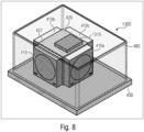
- Fig. 8 shows a MEMS device with an additional MEMS die or integrated circuitry on a top side face region 427 of the carrier structure of the MEMS device, according to embodiments of the disclosure.
- MEMS device 1300 comprises, in contrast to MEMS device 500, as explained in the context of Fig. 5 , an additional MEMS die or integrated circuitry (element 1310) a top side face region of the carrier structure 420.
- the top side face region may, for example as shown in Fig. 8 , be a side face region of the plurality of angularly offset side face regions that may be parallel to a second side face region configured for a coupling of the carrier structure 420 to the substrate 430.
- embodiments comprise an ASIC/MEMS on the top edge of the carrier structure.
- device 1300 may comprise interconnections that may be configured to electrically couple element 1310, e.g. in the form of integrated circuitry, to any or all of the MEMS dies 410, 410a, 410b, 410c.
- element 1310 is an ASIC
- additional ASICs on the substrate 430 e.g. for a provision or analysis of signals from the MEMS dies 410, 410a, 410b, 410c may not be present.
- a carrier structure may comprise a hexagonal base area.
- a carrier structure may comprise a plurality of angularly offset side face regions with respective openings.
- 6 or more MEMS dies may, for example be mounted to the plurality of side face regions.
- Additional MEMS dies may, for example be mounted to a top side face region, e.g. to one of the two side face regions substantially perpendicular to the side face regions.
- embodiments may comprise a 6+ MEMS carrier, with a hexagon arrangement.
- Such a carrier structure may be attached to a substrate using one of the two side face regions substantially perpendicular to the side face regions.
- Fig. 9 shows an example of a carrier structure in the form of a pyramid arrangement according to embodiments of the disclosure. As shown in Fig. 9 , adjacent angularly offset side face regions of a carrier structure 1520 may not necessarily be perpendicular to each other. As explained before, a MEMS die 1510 may be mounted to the carrier structure 1520.
- Fig. 10a shows schematic views of a MEMS device with a first pyramidal carrier structure according to embodiments of the disclosure.
- Fig. 10a d) shows a schematic three-dimensional view of MEMS device 1000.
- Fig. 10a a) shows a schematic side view (e.g. in a x-z plane) of MEMS device 1000 comprising a pyramidal carrier structure 1010.
- the MEMS device 1000 may comprise a plurality of MEMS dies 1020a-d that are mounted to respective side face regions 1010a-d of the carrier structure 1010.
- the side face regions 1010a-d of carrier structure 1010 may be tilted with respect to a bottom side face region (e.g. second side face region) 1060 that may be configured to be coupled to a substrate.
- a bottom side face region e.g. second side face region
- the pyramidal carrier structure 1010 may be flattened or leveled, such that additional circuitry may, for example, be mounted to a top (e.g. flattened top of the pyramidal structure) side face region 1030.
- side face region 1030 may as well comprise a further MEMS die and for example an opening.
- Fig. 10a c) shows a schematic bottom view (e.g. in a x-y plane from a negative z-direction) of MEMS device 1000.
- the bottom side face region 1060 may comprise an opening 1040 to an inner volume of the carrier structure 1010.
- the opening 1040 may, for example, be aligned with a sound port of a substrate, when the carrier structure 1010 is bonded to the substrate, hence allowing an interaction of the inner volume of the carrier structure and a surrounding of the MEMS device 1000. Additionally, through opening 1040, openings 1050a-d in the side face regions are shown. As shown in Fig. 10a , the MEMS dies 1020a-d may span respective openings 1050a-d in the carrier structure 1010. Therefore, MEMS dies 1020a-d may interact with a surrounding of the MEMS device, e.g. via the openings 1050a-d, the opening 1040, and for example an opening, e.g. a sound port, in a respective substrate, the carrier structure may be attached to.
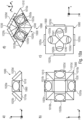
- Fig. 10b shows schematic views of the pyramidal carrier structure according to Fig. 10a .
- Fig. 10b shows respective views (a) schematic side view, b) schematic top view, c) schematic bottom view) of the carrier structure 1010 of MEMS device 1000 according to Fig. 10a .
- the carrier structure 1010 may, for example, be a monolithic carrier structure, e.g. manufactured from one piece.
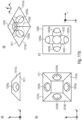
- Fig. 11a shows schematic views of a MEMS device with a second pyramidal carrier structure according to embodiments of the disclosure.
- MEMS device 1001 may comprise a carrier structure 1011.
- Carrier structure 1011 may comprise the features explained in the context of Fig. 10a , but may comprise a different inner structure, compared to carrier structure 1010 as shown in Fig. 10a .
- Fig. 11b shows schematic views of the pyramidal carrier structure according to Fig. 11a .
- the carrier structure may comprise holes (e.g. forming the openings), that may, for example, be perpendicular to a surface of a respective side face region (e.g. hole associated with opening 1020a and side face region 1010a).
- the holes may hence provide the opening 1040 to the inner volume and a respective structure 1041 of the surface of the carrier structure 1010 neighboring the inner volume.
- carrier structure 1011 shown in Fig. 11a may be manufactured differently.
- a hole may be drilled or etched from a bottom surface region 1060 yielding inner structure 1042, e.g.
- a result 1042 of a drilling from the "bottom" e.g. from side face region 1060 in contrast to a result 1041 of trajectories from multiple drilling from the side face regions 1010a-d.
- a hole from the "bottom” may be deep enough to leave the round mark 1042.
- the examples shown in Figs. 10a and 10b may result from only drilling through side face regions 1010a-d, or from first drilling from a bottom side face region 1060, but not deep enough to leave a mark 1042 and subsequent drilling from the side face regions 1010a-d.
- the inner structure of the carrier structure may comprise any form suitable.
- the inner structure may, for example, comprise a structure or form depending on a corresponding manufacturing method, used for providing the carrier structure.
- embodiments according to the disclosure are not limited to a specific manufacturing method or for example, order of manufacturing steps.
- an injection molded carrier structure may comprise a smooth inner surface without the structure shown in Figs. 10a or 11a or respectively as shown in Figs 10b or 11b .
- Fig. 12 shows an example for a three-dimensional rendering of the MEMS device shown in Fig. 10a or Fig. 11a and Figs. 13a and 13b show examples for three-dimensional renderings of the carrier structures shown in Fig. 10b and Fig. 11b respectively.
- a pyramidal arrangement e.g. as shown in Figs. 10 to 13 may allow to achieve a reduced height (e.g. z-dimension), for example, with a similar SNR or sensitivity, compared to a cubic arrangement.
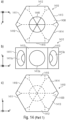
- Fig. 14 shows schematic views of a carrier structure with a hexagonal base area according to embodiments of the disclosure.
- Fig. 14 d) shows a schematic three-dimensional view of carrier structure 1410.
- Figs. 14 a), b) and c) show schematic bottom (e.g. in a x-y plane from a negative z direction), side (e.g. in a x-z plane) and top views (e.g. in a x-y plane from a positive z direction) of carrier structure 1410 having a plurality of angularly offset side face regions 1411, 1412, 1413, 1414, 1415, 1416 with respective openings 1411a, 1412a, 1413a, (1414a, 1415a, not shown) 1416a.
- the carrier structure 1410 may comprise a top side face region 1420, e.g. a side face region substantially perpendicular to the side face regions 1411, 1412, 1413, 1414, 1415, 1416.
- side face region 1420 may comprise integrated circuitry and/or another opening, e.g. to be spanned by a MEMS die.
- a bottom side face region 1430 e.g. a second side face region may comprise an opening 1440 to an inner volume of the carrier structure 1410.
- side face region 1430 may be configured to be coupled with a substrate, e.g. a substrate with a sound port, wherein the sound port may be aligned with the opening 1440.
- Fig. 15 shows an example for a three-dimensional rendering of the carrier structure shown in Fig. 14 .
- Fig. 16 shows schematic views of a MEMS device with a rectangular base area according to embodiments of the disclosure.
- Carrier structure 1610 comprises a plurality of angularly offset side face regions 1611, (1612, 1613, not shown) 1614 providing an inner volume, wherein the side face regions have respective openings 1611a, 1611b, 1612a, 1613a, 1613b, 1614a.
- side face regions 1611 and 1613 comprise two openings each.
- two MEMS dies may be mounted or attached to each of the side face regions 1611 and 1613, each spanning a respective opening.
- one side face region may comprise a plurality of openings and a plurality of MEMS dies spanning the openings.
- Carrier structure 1610 further comprises a bottom side face region 1630 with an opening 1640.
- Carrier structure 1610 may be configured to carry up to 6 MEMS dies and a corresponding ASIC, e.g. on side face region 1620.
- Fig. 17 shows an example for a three-dimensional rendering of the carrier structure shown in Fig. 16 .
- embodiments according to the disclosure comprise MEMS devices, e.g. microphones comprising or containing multiple MEMS dies in one package placed not planar relative to the substrate but out of its plane and acoustically sealed.
- embodiments may be based on the principle to place MEMS dies not planar relative to a substrate surface but out of the substrate plane, e.g. out of a x-y plane, and for example to acoustically seal a package comprising the microphone comprising the MEMS dies.
- embodiments according to the disclosure may provide high performance MEMS microphones, e.g. microphones for a high performance segment of a MEMS microphone market.
- device and/or system characteristics e.g. characteristics of a package comprising a MEMS device according to embodiments
- This may allow new use-cases.
- embodiments of the disclosure may comprise packaged MEMS devices, e.g. a package comprising any of the MEMS devices as discussed herein.
- Embodiments according to the disclosure may comprise microscopic elements, e.g. small elements.
- embodiments according to the disclosure may achieve or even surpass performances of MEMS devices having or using multiple MEMS dies arranged on one substrate in a planar way, for example while providing a smaller footprint (e.g. with respect to a substrate surface).
- embodiments relate to an arrangement of at least one MEMS die "out of plane” (or on a plane that would not be parallel to the plane of the package substrate) by means of the carrier structure.
- further MEMS dies and/or ASIC dies may also be provided on any of the remaining faces of the carrier structure (e.g. except the face used to attach the carrier structure to the package substrate).
- Embodiments according to the disclosure comprise a MEMS device, the MEMS device comprising a MEMS die, and a carrier structure having an inner volume, wherein the carrier structure comprises a plurality of angularly offset side face regions for providing the inner volume.
- the MEMS die is mounted to a first side face region of the plurality of angularly offset side face regions and the MEMS die spans an opening in the first side face region.
- a second side face region of the plurality of angularly offset side face regions, different from the first side face region forms a basis portion for mechanically coupling the carrier structure to a substrate.
- the second side face region and the first side face region are non-parallel to each other.
- the carrier structure comprises an opening to the inner volume of the carrier structure.
- normal vectors of adjacent side face regions of the plurality of angularly offset side face regions are non-parallel.
- the MEMS device comprises a further MEMS die; and the further MEMS die is mounted to the first side face region and the further MEMS die spans the opening or a further opening in the first side face region.
- the MEMS device comprises an additional MEMS die, and the additional MEMS die is mounted to a third side face region of the plurality of angularly offset side face regions, and the additional MEMS die spans an opening in the third side face region.
- the MEMS device further comprises an integrated circuitry, wherein the integrated circuitry is mounted to a side face region of the plurality of angularly offset side face regions.
- the integrated circuitry is electrically coupled to the MEMS die, and the integrated circuitry is configured to process at least one signal provided by the MEMS die and/or the integrated circuitry is configured to provide a stimulus signal to the MEMS die.
- the carrier structure is a monolithic carrier structure and/or the carrier structure is made from a one-piece structure and/or the carrier structure is an injection molded carrier structure and/or the carrier structure is an additively manufactured carrier structure (e.g. a 3-D printed carrier structure).
- the MEMS device is a MEMS microphone and the inner volume of the carrier structure forms a front volume of the MEMS microphone. (e.g. providing or for a bottom-port configuration)
- the MEMS device is a MEMS microphone and the inner volume of the carrier structure forms a back volume of the MEMS microphone. (e.g. providing or for a top-port configuration)
- the MEMS device comprises a plurality of MEMS dies, wherein each MEMS die is mounted to a different side face region of the plurality of angularly offset side face regions.
- the side face regions, to which the plurality of MEMS dies are mounted to are substantially perpendicular to the second side face region.
- At least one of the MEMS dies comprises a sound transducer, an inertial sensor, a pressure sensor and/or a gas sensor.
- the MEMS die comprises a piezoelectric MEMS sound transducer and/or a capacitive MEMS sound transducer.
- the MEMS device further comprises a substrate, wherein the carrier structure is mechanically coupled to the substrate via the second side face region.
- the MEMS device further comprises a lid, wherein the lid is mechanically coupled to the substrate, forming an acoustically sealed back volume or forming a front volume.
- the substrate or the lid comprises a sound port.
- control circuitry can be implemented in hardware or in software or at least partially in hardware or at least partially in software.
- control circuitry can be implemented as a computer program product with a program code, the program code being operative for performing one of the methods when the computer program product runs on a computer.
- the program code may for example be stored on a machine readable carrier.
Landscapes
- Physics & Mathematics (AREA)
- Engineering & Computer Science (AREA)
- Acoustics & Sound (AREA)
- Signal Processing (AREA)
- Micromachines (AREA)
Abstract
Description
- Embodiments according to the present disclosure are concerned with a MEMS device (MEMS = microelectromechanical system) with a carrier structure comprising a plurality of angularly offset side face regions.
- With increasing requirements with regard to miniaturization and functionality, providing new concepts for MEMS devices is challenging. As an example, signal-to-noise ratio (SNR) in MEMS microphones is limited partly by the size of sensitive elements. For example, dimensions of a MEMS die may define capacitances in capacitive MEMS microphones. One approach to overcome this limit is an integration of multiple MEMS in one package.
- As an example,
Fig. 18 shows a schematic side view of a e.g. typical MEMS device (e.g., MEMS microphone). TheMEMS device 1600 comprises aMEMS die 1610, e.g. a sound transducer, and asubstrate 1620, e.g. a substrate of the package, wherein theMEMS die 1610 is attached to thesubstrate 1620. TheMEMS die 1610 comprises asupport structure 1612 and a membrane 1614 (e.g. + backplate, etc.) and anelectrical contact 1616. Thesupport structure 1612 is clamping or holding the membrane 1614 (+ further membranes and/or backplates e.g. in case of capacitive MEMS microphones). Thesubstrate 1620 comprises asound port 1622, e.g. an opening, for example of the packaged MEMS device. Note: A package lid and an ASIC ofdevice 1600 are not illustrated. In some cases, the MEMSdie 1610 may, for example, be integrated, e.g. directly, in thesubstrate 1620. - Known solutions imply planar integration of sensitive elements side by side.
- However, this approach leads to an increased footprint of the microphone and usually requires multiple sound ports and therefore more complicated device sound channel.
- Hence, there is a need for a concept for a MEMS device providing an improved compromise between a signal-to-noise ratio and a complexity of the device.
- Embodiments according to the disclosure comprise a MEMS device, the MEMS device comprising a MEMS die, and a carrier structure having an inner volume, wherein the carrier structure comprises a plurality of angularly offset side face regions for providing the inner volume. The MEMS die is mounted to a first side face region of the plurality of angularly offset side face regions and the MEMS die spans an opening in the first side face region. Furthermore, a second side face region of the plurality of angularly offset side face regions, different from the first side face region, forms a basis portion for mechanically coupling the carrier structure to a substrate.
- The inventors of the embodiments as described in the present application have recognized that a MEMS device comprising a carrier structure may allow to facilitate an integration of MEMS dies in the MEMS device, for example with only limited increase in required space, for example especially lateral space, e.g. parallel to a substrate of the MEMS device, e.g. a lateral space defining a footprint of the MEMS device. In addition, using a carrier structure according to embodiments may allow to achieve high signal-to-noise ratios, for example even in case of highly integrated MEMS devices with many MEMS dies.
- Therefore, the carrier structure comprises an inner volume and a plurality of angularly offset side face regions for providing the inner volume. At least one MEMS die is mounted to a first side face region of the plurality of angularly offset side face regions, the MEMS die spanning an opening in the first side face region. A second side face region of the plurality of angularly offset side face regions, different from the first side face region, forms a basis portion for mechanically coupling the carrier structure to a substrate.
- In simple words, the carrier structure, e.g. a cubic carrier structure, for example an interposer device or an interposer structure, may be a three-dimensional framework extending itself out of a substrate plane (e.g. in an assembled state of the MEMS device, wherein the MEMS device may, for example, be attached, or bonded to a substrate). Consequently, additional, for example approximately or substantially perpendicular (e.g. to a substrate surface) carrier planes, in the form of the side face regions of the carrier structure, are provided, to which MEMS dies may be attached or mounted or bonded or glued.
- In other words, according to embodiments, MEMS dies may be integrated three-dimensionally, e.g. out of a substrate plane, for example out of a plane parallel to a substrate of the MEMS device, or a plane of the MEMS device that may be parallel to a substrate surface in an assembled state. Hence, MEMS dies may be integrated in the MEMS device out of plane. This may allow usage of volumetric space of the MEMS device without increasing its footprint, for example significantly.
- Hence, the carrier structure may comprise openings in respective side face regions, to allow for an interaction of a respective MEMS die, e.g. in the form of a transducer, with an environment of the MEMS device (e.g. via the inner volume). As an example, the inner volume of the carrier structure may, for example, be coupled to an environment of the MEMS device via a port e.g. a sound port, e.g. in a substrate (e.g. coupled with the second side face region). Optionally, the one or more openings in the side face regions may, for example, be holes through the carrier structure (e.g. wholly through a respective side face or side wall or side structure of the carrier structure). As another optional feature, the one or more MEMS dies may share a common sound port. In other words, a plurality of MEMS dies spanning respective openings in respective side face regions may share one, e.g. single, sound port, for example for an interaction (e.g. signal detection or measurement) with a surrounding of the MEMS device.
- As an example, the MEMS device may be a, for example, high SNR, MEMS microphone with 3D integrated sensitive elements. In such a form, the MEMS microphone may achieve a high SNR using an integration of a plurality of MEMS dies in the form of MEMS sound transducers using the carrier structure, e.g. such that the plurality of MEMS sound transducers is 3D integrated. Hence, embodiments may comprise a 3D integration of MEMS for high SNR microphones.
- In the following, embodiments of the present disclosure are described in more detail with respect to the figures, in which:
- Fig. 1
- shows a schematic side view of a MEMS device according to embodiments of the present disclosure;
- Fig. 2
- shows a schematic side view of a MEMS device with additional, optional features, according to embodiments of the present disclosure;
- Figs. 3a-d
- show schematic side views of MEMS devices with optional features, according to embodiments of the present disclosure;
- Fig. 4
- shows a schematic three-dimensional view of examples of manufacturing steps for a MEMS device according to embodiments of the disclosure;
- Fig. 5
- shows a schematic three-dimensional view of an example for a MEMS device according to the manufacturing steps shown in
Fig. 4 ; - Fig. 6
- shows a schematic view of a carrier structure design variant according to embodiments of the disclosure;
- Figs. 7
- show an example for interconnections according to embodiments of the disclosure;
- Fig. 8
- shows a MEMS device with an additional MEMS die or integrated circuitry on a top side face region of the carrier structure of the MEMS device, according to embodiments of the disclosure;
- Fig. 9
- shows an example of a carrier structure in the form of a pyramid arrangement according to embodiments of the disclosure;
- Fig. 10a
- shows schematic views of a MEMS device with a first pyramidal carrier structure according to embodiments of the disclosure;
- Fig. 10b
- shows schematic views of the first pyramidal carrier structure according to
Fig. 10a ; - Fig. 11a
- shows schematic views of a MEMS device with a second pyramidal carrier structure according to embodiments of the disclosure;
- Fig. 11b
- shows schematic views of the second pyramidal carrier structure according to
Fig. 11a ; - Fig. 12
- shows an example for a three-dimensional rendering of the MEMS device shown in
Fig. 10a or11a ; - Fig. 13a
- shows an example for a three-dimensional rendering of the carrier structure shown in
Fig. 10b ; and - Fig. 13b
- shows an example for a three-dimensional rendering of the carrier structure shown in
Fig. 11b ; and - Fig. 14
- shows schematic views of a MEMS device with a hexagonal base area according to embodiments of the disclosure;
- Fig. 15
- shows an example for a three-dimensional rendering of the carrier structure shown in
Fig. 14 ; - Fig. 16
- shows schematic views of a MEMS device with a rectangular base area according to embodiments of the disclosure;
- Fig. 17
- shows an example for a three-dimensional rendering of the carrier structure shown in
Fig. 16 ; - Fig. 18
- shows a schematic side view of a typical MEMS device (e.g., MEMS microphone).
- In the following description, embodiments are discussed in further detail using the figures, wherein in the figures and the specification identical elements and elements having the same functionality and/or the same technical or physical effect are provided with the same reference numbers or are identified with the same name. Thus, the description of these elements and of the functionality thereof as illustrated in the different embodiments are mutually exchangeable or may be applied to one another in the different embodiments.
- In the following description, embodiments are discussed in detail, however, it should be appreciated that the embodiments provide many applicable concepts that can be embodied in a wide variety of semiconductor devices. The specific embodiments discussed are merely illustrative of specific ways to make and use the present concept, and do not limit the scope of the embodiments. In the following description of embodiments, the same or similar elements having the same function have associated therewith the same reference signs or the same name, and a description of such elements will not be repeated for every embodiment. Moreover, features of the different embodiments described hereinafter may be combined with each other, unless specifically noted otherwise.
- It is understood that when an element is referred to as being "connected" or "coupled" to another element, it may be directly connected or coupled to the other element, or intermediate elements may be present. Conversely, when an element is referred to as being "directly" connected to another element, "connected" or "coupled," there are no intermediate elements. Other terms used to describe the relationship between elements should be construed in a similar fashion (e.g., "between" versus "directly between", "adjacent" versus "directly adjacent", and "on" versus "directly on", etc.).
- For facilitating the description of the different embodiments, some of the figures comprise a Cartesian coordinate system x, y, z, wherein the x-y-plane corresponds, i.e. is parallel, to a reference plane (= x-y-plane), e.g. a main surface region of a substrate, wherein the direction vertically up with respect to the reference plane (x-y-plane) corresponds to the "+z" direction, and wherein the direction vertically down with respect to the reference plane (x-y-plane) corresponds to the "-z" direction. In the following description, the term "lateral" means a direction parallel to the x- and/or y-direction or a direction parallel to (or in) the x-y-plane, wherein the term "vertical" means a direction parallel to the z-direction.
-
Fig. 1 shows a schematic side view of a MEMS device according to embodiments of the present disclosure.Fig. 1 shows aMEMS device 100 comprising a MEMS die 110 and acarrier structure 120. The carrier structure comprises aninner volume 121 and a plurality of angularly offsetside face regions inner volume 121. The MEMS die 110 is mounted to a firstside face region 122 of the plurality of angularly offset side face regions. Furthermore, the MEMS die 110 spans anopening 122a in the first side face region. A secondside face region 123 of the plurality of angularly offset side face regions, different from the first side face region, forms a basis portion for mechanically coupling the carrier structure to a substrate. - As an optional feature, the second side face region comprises an
opening 123a to theinner volume 121 of the carrier structure, however it is to be noted that according to other embodiments of the disclosure such anopening 123a may not be present, thedevice 100 hence having a "closed"side face region 123, e.g. according to or analogously to or similar to theside face regions Fig. 1 , the MEMS die may, for example, be in contact with an environment of theMEMS device 100, e.g. via theopening 123a. According to different embodiments of the disclosure, theinner volume 121 may, for example, be a closed volume. In such an embodiment, a MEMS die 110 may, for example be directly in contact with an environment of theMEMS device 100. With regard to microphone applications, e.g. in case MEMS die 110 is a sound transducer, theinner volume 121 may, for example, be a front volume or, e.g. incase opening 123a is not present a back volume. - Furthermore, it is to be noted that the particular arrangement shown in
Fig. 1 with a specific number of side face regions, e.g. withside face regions device 100 according to embodiments may comprise a cubic carrier structure, for example as shown inFig. 1 , or a pyramidal carrier structure, for example having less side face regions than shown inFig. 1 . In general, the carrier structure may, for example, be a polyhedron. - Optionally, the carrier structure may, for example, be a monolithic and/or integral carrier structure. As an example, the carrier structure may be made or fabricated from one piece. In other words, the carrier structure may be etched or manufactured from one workpiece, e.g. from a one-piece structure, e.g. in contrast to a carrier structure comprising a plurality of partial structures that were bonded or wielded or glued or soldered together or that were, for example, connected to each other with hinges and/or latches. This way, the carrier structure may be produced with low effort, and for example with good mechanical properties, e.g. with good mechanical rigidity.
- Alternatively or in addition, the carrier structure may be an injection molded carrier structure and/or an additively manufactured carrier structure (e.g. a 3-D printed carrier structure).
- According to embodiments, e.g. as shown in
Fig. 1 , a main idea is the integration of MEMS dies 110 out of plane, for example, according toFig. 1 out of the x-y plane, such that, in an assembled state, the MEMS die 110 is out of plane to a substrate. The MEMS die 110 may, for example, be substantially perpendicular to a substrate plane, e.g. the x-y plane, e.g. with a tolerance of less than 1° or of less than 5° or of less than 10° (e.g. measured to the y-z plane). - Hence,
device 100 may comprise a plurality of MEMS dies 110, attached to different side face regions of the device. In this case, the side face regions, having MEMS dies 110 attached to, may comprise openings, e.g. analogously toside face region 122 withopening 122a. Hence, a footprint, e.g. an area of theMEMS device 100 with respect to the x-y plane, may not be increased or may, for example, be increased only in a limited way, whilst providing a plurality of, e.g. out of plane, MEMS dies. As an example, for the case ofMEMS device 100 being MEMS microphone, and MEMS dies 110 being MEMS sound transducers, a high SNR with a e.g. very low footprint may be achieved. - Optionally, e.g. as shown in
Fig. 1 , the secondside face region 123 and the firstside face region 122 may be non-parallel to each other. As an example, the secondside face region 123 and the firstside face region 122 may be non-parallel and adjacent to each other. However, MEMS die 110 may, for example, be attached toside face region 124 instead ofside face region 122. In general, for example, in a cubic carrier structure, a MEMS die can, for example, be arranged on top of the carrier structure, e.g. the cube. This side face region, e.g. 124, may, for example, be parallel, or substantially parallel, to the second, e.g. bottom side face region, e.g. 123, of the carrier structure, e.g. in the form of a cube (e.g. to the second side face region which may be configured to couple thecarrier structure 120 to a substrate). As an example, second side face region, e.g. the coupling side face region, and any side face region where a MEMS die or for example an ASIC die are provided, may be different planes or may, for example be in different planes. - As another optional feature, normal vectors of adjacent side face regions of the plurality of angularly offset side face regions may be non-parallel. As an example with respect to
Fig. 1 , a vector perpendicular to the y-z plane for theside face region 122 and a vector perpendicular to the x-y plane for theside face region 124, may be non-parallel. In simple words, adjacent side face regions may comprise an angular offset, for example such that their respective normal vectors are non-parallel. -
Fig. 2 shows a schematic side view of a MEMS device with additional optional features, according to embodiments of the present disclosure.Fig. 2 shows aMEMS device 200 with at least one MEMS die 210, e.g. a sound transducer, and acarrier structure 220. Thecarrier structure 220 comprises a plurality of angularly offsetside face regions 226, for providing aninner volume 221, as an example, theside face regions side face region 222, theside face region 222 comprising anopening 222a. - In other words, and in general, according to embodiments of the disclosure, a
MEMS device 200 may comprise aplurality 226 of side face regions, e.g. faces, including or comprising at least oneside face region 222 onto which aMEMS die 210 is provided. - As shown, optionally, other side face regions, e.g.
side face region 223,side face region 224 and/orside face region 225 may compriseopenings side face region 223 configured to be coupled with a substrate) can be configured to optionally accommodate a further or another semiconductor chip (e.g., additional MEMS dies and/or ASIC dies). It is to be noted, that optionally one or more ASIC dies could be provided on a respective side face region of the structure, and/or on the substrate, the substrate for example being a package substrate, e.g. a substrate comprising packageddevice 200. Furthermore, it is to be noted, that integrated circuitry, e.g. in the form of an ASIC may be mounted to side face regions having no opening or to side face regions having an opening, e.g. besides a MEMS die spanning said opening. - As an optional feature, the MEMS die 210 comprises a support structure 212 (e.g. of the individual MEMS die 210) and a membrane 214 (e.g. comprising a backplate and/or further elements). The
membrane 214 may, for example be an active part of the MEMS die 210 or theMEMS device 200. - As another optional feature, the
MEMS device 200 comprises anelectrical contact 230. The electrical contact may be configured to connect the MEMS die 210 with circuitry of the MEMS device 200 (not shown) or external circuitry, e.g. of a package comprising theMEMS device 200. - Optionally, as shown in
Fig. 2 , theMEMS device 200 comprises asubstrate 240, e.g. a carrier substrate. This substrate may as well be a substrate of a package, e.g. a package comprising thedevice 200. As another optional feature,substrate 240 comprises asound port 242, e.g. a common and/or shared sound port, e.g. a common or shared opening, for example, of the packaged MEMS device. - It is to be noted that an optional package lid and ASIC are not illustrated in
Fig. 2 . -
Fig. 3a shows a schematic side view of a first MEMS device with optional features, according to embodiments of the present disclosure.MEMS device 300a comprises acarrier structure 320 having an inner volume 321 and angularly offsetside face regions - The first
side face region 322 comprises anopening 322a and, as an optional feature, afurther opening 322b. TheMEMS device 300a comprises a MEMS die 310 that is mounted to the firstside face region 322, spanning theopening 322a. As another optional feature,device 300a comprises a further MEMS die 310a that is mounted to the firstside face region 322 and that spans thefurther opening 322b. In general, and as illustrated in the example shown inFig. 3 , more than one MEMS die may be mounted or attached or bonded or glued to a respective side face region of the plurality of side face regions of the carrier structure. This may allow to further increase the packing density of MEMS dies in a MEMS device according to embodiments. It is to be noted, that to more than one side face regions, a plurality of MEMS dies may be mounted. In addition, MEMS die 310a may optionally span opening 322a. - As explained before, the second
side face region 323 of the plurality of angularly offset side face regions, different from the firstside face region 322, forms a basis portion for mechanically coupling thecarrier structure 320 to a substrate. As an example, e.g. as discussed in the context ofFig. 2 side face region 323 comprises anopening 323a. Optionally, as shown, theMEMS device 300a may comprise thesubstrate 340 and hence, thecarrier structure 320 may be mechanically coupled or bonded or glued or attached to thesubstrate 340 via the secondside face region 323. - As another optional feature, the
MEMS device 300a comprises an additional MEMS die 310b, wherein the additional MEMS die 310b is mounted to the thirdside face region 324 of the plurality of angularly offset side face regions, and wherein the additional MEMS die 310b spans anopening 324a in the thirdside face region 324. - As another optional feature, the
MEMS device 300a comprises anintegrated circuitry 360, wherein the integrated circuitry is mounted to a side face region, as an example, as shown inFig. 3a , toside face region 325, of the plurality of angularly offset side face regions. Optionally, theintegrated circuitry 360 is electrically coupled to the MEMS die 310 and/or any of the other MEMS dies 310a, 310b, and/or theintegrated circuitry 360 may be configured to process at least one signal provided by the MEMS die 310 (and/or 310a, 310b) and/or theintegrated circuitry 360 may be configured to provide a stimulus signal to the MEMS die 310 (and/or 310a, 310b). - As another optional feature, the
substrate 340 comprises asound port 342. The sound port may allow a coupling of the inner volume 321 with an environment of theMEMS device 300a. Optionally, one of the MEMS dies 310,310a 310b may, for example comprise a piezoelectric MEMS sound transducer and/or a capacitive MEMS sound transducer. Hence, an environmental influence, e.g. a sound wave, may enter the inner volume 321 of thecarrier structure 320 via theoptional sound port 342, where it may be detected using at least one of the MEMS dies 310, 310a, 310b. - In general and as an example, at least of the MEMS dies 310,
310a 310b may comprise a sound transducer, an inertial sensor, a pressure sensor and/or a gas sensor. - However, it is to be noted that
device 300a may comprise MEMS dies mounted to any of the side face regions that do not span an opening in the respective side face region. As an example, one of the MEMS dies 310, 310a or 310b may, for example, be an inertial sensor that may not require a contact with an environmental gas in order to provide a measurement. Hence, such a sensor may be mounted or attached to a side face region without spanning a respective opening. - As another optional feature, the
MEMS device 300a further comprises alid 350, wherein thelid 350 is mechanically coupled to the substrate. As shown inFig. 3 with thesubstrate 340 comprising thesound port 342, the lid may form an acoustically sealed back volume. E.g. in this case, theMEMS device 300a may, for example, be a MEMS microphone and the inner volume 321 of thecarrier structure 320 may form a respective front volume of the MEMS microphone. Hence,Fig. 3a may show a bottom-port configuration of a MEMS microphone according to embodiments. An inventive structure according toFig. 3a may allow to provide a big back volume in order to record a received acoustic signal with a good signal-to-noise ratio. -
Fig. 3b shows a schematic side view of a second MEMS device with optional features, according to embodiments of the present disclosure. In contrast toFig. 3a ,MEMS device 300b comprises asubstrate 340b without a sound port. As an optional feature,lid 350b, that may be mechanically coupled to thesubstrate 340b, comprises asound port 352. Hence, e.g. in case theMEMS device 300b is a MEMS microphone, thelid 350b, coupled to thesubstrate 340b, may form a front volume, e.g. of the MEMS microphone. Accordingly, for example in said case of a MEMS microphone, theinner volume 321b of thecarrier structure 320 may form a back volume of the MEMS microphone. Hence,Fig. 3a may show a top-port configuration of a MEMS microphone according to embodiments. -
Fig. 3c shows a schematic side view of a third MEMS device with optional features, according to embodiments of the present disclosure. In contrast toFigs. 3a and3c , the MEMS dies 310, 310a and 310b theintegrated circuitry 360 are arranged in theinner volume 321c of thecarrier structure 320. As an example, MEMS die 310 is mounted to a firstside face region 326, spanning anopening 326a, MEMS die 310a is mounted to the firstside face region 326 as well, optionally spanning afurther opening 326b in the first side face region and MEMS die 310b is mounted to a thirdside face region 328 spanning arespective opening 328a. The integrated circuitry, e.g. in general an ASIC, is mounted to a fourthside face region 329. A secondside face region 327, optionally comprising anopening 327a, is coupled mechanically withsubstrate 340c. - It is to be noted that some or all MEMS dies and/or integrated circuitry may be mounted to an inside of the carrier structure or to an outside of the carrier structure (e.g. as shown in
Figs. 3a-c ). Hence any combination of the different attachments may be realized according to embodiments. -
Fig. 3d shows a schematic side view of a fourth MEMS device with optional features, according to embodiments of the present disclosure.MEMS device 300d comprisescarrier structure 322d comprising a plurality of angularly offsetside face regions inner volume 321d. As another optional feature,MEMS device 300d comprises a plurality of MEMS dies 310, 310c, wherein each MEMS die is mounted to a different side face region of the plurality of angularly offset side face regions. - As another optional feature, the
side face regions side face region 323d. As shown as an example, it is to be noted that a MEMS dies 310b may as well be mounted toside face regions 324d substantially parallel to the secondside face region 323d. -
Fig. 4 shows a schematic three-dimensional view of examples of manufacturing steps for a MEMS device according to embodiments of the disclosure.Fig. 4 may show an example for a main technical implementation of an embodiments according to the disclosure. - As shown in the top row of
Fig. 4 a plurality of MEMS dies 410, 410a, 410b, 410c may be attached or mounted to a carrier structure 420 ("MEMS (die) to carrier (structure) attach"). As shown, the carrier structure may compriseopenings side face regions side face region 427 may, for example be a top side face region. The MEMS dies 410, 410a, 410b, 410c may be mounted to respective side faceregions respective opening - As shown in the middle row of
Fig. 4 , for example, as a next step, thecarrier structure 420, optionally as shown with mounted MEMS dies 410, 410a, 410b, 410c may be attached or soldered or mounted to asubstrate 430, e.g. a PCB (printed circuit board), for example, comprising integrated circuitry, e.g. as shown ASICs 440a, 440c ("Carrier/ASIC to PCB attach"). It is to be noted that the integrated circuitry may, for example, be attached to thesubstrate 430 after attaching thecarrier structure 420 or vice versa. - As shown in the bottom row of
Fig. 4 , for example, as a next step,interconnections 450, e.g. electrical contacts, e.g. as explained in the context ofFig. 2 , may be added ("Interconnections"). Theinterconnections 450 may, for example, be configured to connect the MEMS dies 410, 410a, 410b, 410c to conductor tracks (not shown) of thesubstrate 430, that may, for example, be electrically coupled with integrated circuitry, e.g. with ASICs 440a, 440b. -
Fig. 5 shows a schematic three-dimensional view of an example for a MEMS device according to the manufacturing steps shown inFig. 4 . As another optional feature,MEMS device 500 comprises alid 460. Hence,device 500 may comprise a plurality of MEMS dies and consequently the steps shown inFig. 4 may allow an out of plane integration of 4+ (4 and more) MEMS chips (e.g. MEMS dies). MEMS dies can be attached to a carrier structure, e.g. carrier, to form a front volume, e.g.inner volume 421, acoustically isolated from a back volume, e.g. a volume arranged between thelid 460 and thesubstrate 430. - As explained with the above example, according to embodiments, devices with high or higher SNR may be provided, keeping a low or for example the same footprint and single sound port, e.g. as a single MEMS single sound port device.
-
Fig. 6 shows a schematic view of a carrier structure design variant according to embodiments of the disclosure, e.g. a carrier design (main variant).Fig. 6 may show a main technical implementation for the carrier structure.Fig. 6 shows aschematic side view 610 of a carrier structure. As an example, the carrier structure may, for example, be a cubic carrier structure, e.g. with an edge length of, e.g. about, 1.8 mm (e.g. with a tolerance of +/-5% or with a tolerance of +/-20%, e.g. with preferred dimensions around, or for example of at least, 0.5 mm to, or for example at most, 2 mm), for example with an edge length of at least 0.3 mm and at most 5 mm or of at least 1.0 mm and at most 2.6 mm or of at least 1.5 mm and at most 2.1 mm. Openings in the side face regions of the carrier structure may, for example, be circular openings, e.g. comprising a diameter of, e.g. about, 1.3 mm (e.g. with a tolerance of +/-5% or with a tolerance of +/-20%, e.g. with preferred dimensions around, or for example of at least, 0.5 mm to, or for example at most, 2 mm), for example with an diameter of at least 0.1 mm and at most 4.5 mm or of at least 0.5 mm and at most 2.1 mm of at least 1.0 mm and at most 1.6 mm. The openings may, for example be offset from an outer edge of the carrier structure by, e.g. about, 0.25 mm (e.g. with a tolerance of +/-5% or with a tolerance of +/-20%, optionally with preferred offsets around, or for example of at least, 0.5 mm to, or for example at most, 2 mm) or by at least 0.25 mm, for example by at least 0.1 mm and by at most 2 mm or by at least 0.2 mm and by at most 0.3 mm or by at least 0.225 mm and by at most 0.275 mm. As an example, as shown inview 610, the openings may, for example, be centered in a respective side face region. However it is to be noted that in general, openings in side face regions do not necessarily have to be centered.Schematic side view 620 shows a cross section through plane A-A ofside view 610, highlighting an offset of the opening from an outer edge. Schematic three-dimensional views 630 and 640 show a carrier structure according toviews -
Figs. 7 may show a main technical implementation according to embodiments of the disclosure, e.g. for a 90 degree wire bonding. Optionally, a wire may be bonded to a MEMS die (or respectively a substrate) of a MEMS device. In the following, the MEMS device (or the bond wire) may be turned, e.g. 90 degree, and bonded to a substrate (or respectively MEMS die) of the MEMS device. An example for a result of such a bonding process is shown inFig. 7. Fig. 7 shows a schematic view of acarrier structure 1220 having aMEMS die 1210, comprising a die pad, mounted to one of its side face regions, wherein aninterconnection 1240 is bonded from the die pad to asubstrate 1230, e.g. in the form of a PCB, e.g. to a PCB pad of the substrate. In other words, a MEMS die may comprise a die pad and the substrate may comprise one or more pads as well. Hence, interconnections between a MEMS die and the substrate may be provided via interconnections in between respective bond pads of the MEMS die and a respective pad of the substrate. - As an example, the carrier structure, may, for example, be a bi-material carrier (e.g. isolating body and conductive interconnects (paths and pad) on it).
-
Figs. 8 to 9 may show alternative technical implementations according to embodiments of the disclosure. -
Fig. 8 shows a MEMS device with an additional MEMS die or integrated circuitry on a topside face region 427 of the carrier structure of the MEMS device, according to embodiments of the disclosure.MEMS device 1300 comprises, in contrast toMEMS device 500, as explained in the context ofFig. 5 , an additional MEMS die or integrated circuitry (element 1310) a top side face region of thecarrier structure 420. The top side face region may, for example as shown inFig. 8 , be a side face region of the plurality of angularly offset side face regions that may be parallel to a second side face region configured for a coupling of thecarrier structure 420 to thesubstrate 430. In simple words, embodiments comprise an ASIC/MEMS on the top edge of the carrier structure. As another optional feature,device 1300 may comprise interconnections that may be configured to electricallycouple element 1310, e.g. in the form of integrated circuitry, to any or all of the MEMS dies 410, 410a, 410b, 410c. As shown inFig. 8 , for example in the case thatelement 1310 is an ASIC, additional ASICs on thesubstrate 430, e.g. for a provision or analysis of signals from the MEMS dies 410, 410a, 410b, 410c may not be present. - As an example, a carrier structure according to embodiments may comprise a hexagonal base area. Accordingly, a carrier structure may comprise a plurality of angularly offset side face regions with respective openings. Hence, 6 or more MEMS dies may, for example be mounted to the plurality of side face regions. Additional MEMS dies, may, for example be mounted to a top side face region, e.g. to one of the two side face regions substantially perpendicular to the side face regions. In simple words embodiments may comprise a 6+ MEMS carrier, with a hexagon arrangement. Such a carrier structure may be attached to a substrate using one of the two side face regions substantially perpendicular to the side face regions.
-
Fig. 9 shows an example of a carrier structure in the form of a pyramid arrangement according to embodiments of the disclosure. As shown inFig. 9 , adjacent angularly offset side face regions of acarrier structure 1520 may not necessarily be perpendicular to each other. As explained before, a MEMS die 1510 may be mounted to thecarrier structure 1520. -
Fig. 10a shows schematic views of a MEMS device with a first pyramidal carrier structure according to embodiments of the disclosure.Fig. 10a d) shows a schematic three-dimensional view ofMEMS device 1000.Fig. 10a a) shows a schematic side view (e.g. in a x-z plane) ofMEMS device 1000 comprising apyramidal carrier structure 1010. As shown in the schematic top view (e.g. in a x-y plane from a positive z direction) inFig. 10a b ), theMEMS device 1000 may comprise a plurality of MEMS dies 1020a-d that are mounted to respectiveside face regions 1010a-d of thecarrier structure 1010. As shown, theside face regions 1010a-d ofcarrier structure 1010, and hence the MEMS dies 1020a-d, may be tilted with respect to a bottom side face region (e.g. second side face region) 1060 that may be configured to be coupled to a substrate. - The
pyramidal carrier structure 1010 may be flattened or leveled, such that additional circuitry may, for example, be mounted to a top (e.g. flattened top of the pyramidal structure)side face region 1030. Optionally,side face region 1030 may as well comprise a further MEMS die and for example an opening.Fig. 10a c) shows a schematic bottom view (e.g. in a x-y plane from a negative z-direction) ofMEMS device 1000. As shown inFig. 10a c) the bottomside face region 1060 may comprise anopening 1040 to an inner volume of thecarrier structure 1010. Theopening 1040 may, for example, be aligned with a sound port of a substrate, when thecarrier structure 1010 is bonded to the substrate, hence allowing an interaction of the inner volume of the carrier structure and a surrounding of theMEMS device 1000. Additionally, throughopening 1040,openings 1050a-d in the side face regions are shown. As shown inFig. 10a , the MEMS dies 1020a-d may spanrespective openings 1050a-d in thecarrier structure 1010. Therefore, MEMS dies 1020a-d may interact with a surrounding of the MEMS device, e.g. via theopenings 1050a-d, theopening 1040, and for example an opening, e.g. a sound port, in a respective substrate, the carrier structure may be attached to. -
Fig. 10b shows schematic views of the pyramidal carrier structure according toFig. 10a .Fig. 10b shows respective views (a) schematic side view, b) schematic top view, c) schematic bottom view) of thecarrier structure 1010 ofMEMS device 1000 according toFig. 10a . Thecarrier structure 1010 may, for example, be a monolithic carrier structure, e.g. manufactured from one piece. -
Fig. 11a shows schematic views of a MEMS device with a second pyramidal carrier structure according to embodiments of the disclosure.MEMS device 1001 may comprise acarrier structure 1011.Carrier structure 1011 may comprise the features explained in the context ofFig. 10a , but may comprise a different inner structure, compared tocarrier structure 1010 as shown inFig. 10a .Fig. 11b shows schematic views of the pyramidal carrier structure according toFig. 11a . - As an example, as shown in
Fig. 10a c), e.g. in combination withFig. 10a d), the carrier structure may comprise holes (e.g. forming the openings), that may, for example, be perpendicular to a surface of a respective side face region (e.g. hole associated withopening 1020a and side faceregion 1010a). The holes may hence provide theopening 1040 to the inner volume and arespective structure 1041 of the surface of thecarrier structure 1010 neighboring the inner volume. As an example,carrier structure 1011 shown inFig. 11a may be manufactured differently. A hole may be drilled or etched from abottom surface region 1060 yieldinginner structure 1042, e.g. aresult 1042 of a drilling from the "bottom", e.g. fromside face region 1060 in contrast to aresult 1041 of trajectories from multiple drilling from theside face regions 1010a-d. As an example, inFigs. 11a and11b a hole from the "bottom" may be deep enough to leave theround mark 1042. On the other hand, the examples shown inFigs. 10a and10b may result from only drilling throughside face regions 1010a-d, or from first drilling from a bottomside face region 1060, but not deep enough to leave amark 1042 and subsequent drilling from theside face regions 1010a-d. - However, it is to be noted, that the inner structure of the carrier structure, may comprise any form suitable. The inner structure may, for example, comprise a structure or form depending on a corresponding manufacturing method, used for providing the carrier structure. Hence, it is to be noted that embodiments according to the disclosure are not limited to a specific manufacturing method or for example, order of manufacturing steps. As an example, an injection molded carrier structure may comprise a smooth inner surface without the structure shown in
Figs. 10a or11a or respectively as shown inFigs 10b or11b . -
Fig. 12 shows an example for a three-dimensional rendering of the MEMS device shown inFig. 10a orFig. 11a andFigs. 13a and13b show examples for three-dimensional renderings of the carrier structures shown inFig. 10b andFig. 11b respectively. - A pyramidal arrangement, e.g. as shown in
Figs. 10 to 13 may allow to achieve a reduced height (e.g. z-dimension), for example, with a similar SNR or sensitivity, compared to a cubic arrangement. -
Fig. 14 shows schematic views of a carrier structure with a hexagonal base area according to embodiments of the disclosure.Fig. 14 d) shows a schematic three-dimensional view ofcarrier structure 1410. -
Figs. 14 a), b) and c) show schematic bottom (e.g. in a x-y plane from a negative z direction), side (e.g. in a x-z plane) and top views (e.g. in a x-y plane from a positive z direction) ofcarrier structure 1410 having a plurality of angularly offsetside face regions respective openings - The
carrier structure 1410 may comprise a topside face region 1420, e.g. a side face region substantially perpendicular to theside face regions side face region 1420 may comprise integrated circuitry and/or another opening, e.g. to be spanned by a MEMS die. - A bottom
side face region 1430, e.g. a second side face region may comprise anopening 1440 to an inner volume of thecarrier structure 1410. As explained before,side face region 1430 may be configured to be coupled with a substrate, e.g. a substrate with a sound port, wherein the sound port may be aligned with theopening 1440.Fig. 15 shows an example for a three-dimensional rendering of the carrier structure shown inFig. 14 . -
Fig. 16 shows schematic views of a MEMS device with a rectangular base area according to embodiments of the disclosure.Carrier structure 1610 comprises a plurality of angularly offsetside face regions 1611, (1612, 1613, not shown) 1614 providing an inner volume, wherein the side face regions haverespective openings side face regions 1611 and 1613 comprise two openings each. Hence, two MEMS dies may be mounted or attached to each of theside face regions 1611 and 1613, each spanning a respective opening. In other words, in general one side face region may comprise a plurality of openings and a plurality of MEMS dies spanning the openings. -
Carrier structure 1610 further comprises a bottomside face region 1630 with anopening 1640.Carrier structure 1610 may be configured to carry up to 6 MEMS dies and a corresponding ASIC, e.g. onside face region 1620.Fig. 17 shows an example for a three-dimensional rendering of the carrier structure shown inFig. 16 . - In general, embodiments according to the disclosure comprise MEMS devices, e.g. microphones comprising or containing multiple MEMS dies in one package placed not planar relative to the substrate but out of its plane and acoustically sealed. In other words, embodiments may be based on the principle to place MEMS dies not planar relative to a substrate surface but out of the substrate plane, e.g. out of a x-y plane, and for example to acoustically seal a package comprising the microphone comprising the MEMS dies. Hence, embodiments according to the disclosure may provide high performance MEMS microphones, e.g. microphones for a high performance segment of a MEMS microphone market.
- As an example, e.g. based on a high SNR of a MEMS device, e.g. in the form of a microphone, according to embodiments, device and/or system characteristics (e.g. characteristics of a package comprising a MEMS device according to embodiments) may be improved. This may allow new use-cases.
- In general, embodiments of the disclosure may comprise packaged MEMS devices, e.g. a package comprising any of the MEMS devices as discussed herein. Embodiments according to the disclosure may comprise microscopic elements, e.g. small elements.
- It is to be noted, that embodiments according to the disclosure may achieve or even surpass performances of MEMS devices having or using multiple MEMS dies arranged on one substrate in a planar way, for example while providing a smaller footprint (e.g. with respect to a substrate surface).
- In general, embodiments relate to an arrangement of at least one MEMS die "out of plane" (or on a plane that would not be parallel to the plane of the package substrate) by means of the carrier structure. Optionally, further MEMS dies and/or ASIC dies may also be provided on any of the remaining faces of the carrier structure (e.g. except the face used to attach the carrier structure to the package substrate).
- Additional embodiments and aspects are described which may be used alone or in combination with the features and functionalities described herein.
- Embodiments according to the disclosure comprise a MEMS device, the MEMS device comprising a MEMS die, and a carrier structure having an inner volume, wherein the carrier structure comprises a plurality of angularly offset side face regions for providing the inner volume. The MEMS die is mounted to a first side face region of the plurality of angularly offset side face regions and the MEMS die spans an opening in the first side face region. Furthermore, a second side face region of the plurality of angularly offset side face regions, different from the first side face region, forms a basis portion for mechanically coupling the carrier structure to a substrate.
- According to further embodiments of the disclosure, the second side face region and the first side face region are non-parallel to each other.
- According to further embodiments of the disclosure, the carrier structure comprises an opening to the inner volume of the carrier structure.
- According to further embodiments of the disclosure, normal vectors of adjacent side face regions of the plurality of angularly offset side face regions are non-parallel.
- According to further embodiments of the disclosure, the MEMS device comprises a further MEMS die; and the further MEMS die is mounted to the first side face region and the further MEMS die spans the opening or a further opening in the first side face region.
- According to further embodiments of the disclosure, the MEMS device comprises an additional MEMS die, and the additional MEMS die is mounted to a third side face region of the plurality of angularly offset side face regions, and the additional MEMS die spans an opening in the third side face region.
- According to further embodiments of the disclosure, the MEMS device further comprises an integrated circuitry, wherein the integrated circuitry is mounted to a side face region of the plurality of angularly offset side face regions.
- According to further embodiments of the disclosure, the integrated circuitry is electrically coupled to the MEMS die, and the integrated circuitry is configured to process at least one signal provided by the MEMS die and/or the integrated circuitry is configured to provide a stimulus signal to the MEMS die.
- According to further embodiments of the disclosure, the carrier structure is a monolithic carrier structure and/or the carrier structure is made from a one-piece structure and/or the carrier structure is an injection molded carrier structure and/or the carrier structure is an additively manufactured carrier structure (e.g. a 3-D printed carrier structure).
- According to further embodiments of the disclosure, the MEMS device is a MEMS microphone and the inner volume of the carrier structure forms a front volume of the MEMS microphone. (e.g. providing or for a bottom-port configuration)
- According to further embodiments of the disclosure, the MEMS device is a MEMS microphone and the inner volume of the carrier structure forms a back volume of the MEMS microphone. (e.g. providing or for a top-port configuration)
- According to further embodiments of the disclosure, the MEMS device comprises a plurality of MEMS dies, wherein each MEMS die is mounted to a different side face region of the plurality of angularly offset side face regions.
- According to further embodiments of the disclosure, the side face regions, to which the plurality of MEMS dies are mounted to, are substantially perpendicular to the second side face region.
- According to further embodiments of the disclosure, at least one of the MEMS dies comprises a sound transducer, an inertial sensor, a pressure sensor and/or a gas sensor.
- According to further embodiments of the disclosure, the MEMS die comprises a piezoelectric MEMS sound transducer and/or a capacitive MEMS sound transducer.
- According to further embodiments of the disclosure, the MEMS device further comprises a substrate, wherein the carrier structure is mechanically coupled to the substrate via the second side face region.
- According to further embodiments of the disclosure, the MEMS device further comprises a lid, wherein the lid is mechanically coupled to the substrate, forming an acoustically sealed back volume or forming a front volume.
- According to further embodiments of the disclosure, the substrate or the lid comprises a sound port.
- Additional embodiments and aspects are described which may be used alone or in combination with the features and functionalities described herein.
- Although some aspects have been described as features in the context of an apparatus it is clear that such a description may also be regarded as a description of corresponding features of a method. Although some aspects have been described as features in the context of a method, it is clear that such a description may also be regarded as a description of corresponding features concerning the functionality of an apparatus.
- Depending on certain implementation requirements, embodiments of the control circuitry can be implemented in hardware or in software or at least partially in hardware or at least partially in software. Generally, embodiments of the control circuitry can be implemented as a computer program product with a program code, the program code being operative for performing one of the methods when the computer program product runs on a computer. The program code may for example be stored on a machine readable carrier.
- In the foregoing detailed description, it can be seen that various features are grouped together in examples for the purpose of streamlining the disclosure. This method of disclosure is not to be interpreted as reflecting an intention that the claimed examples require more features than are expressly recited in each claim. Rather, as the following claims reflect, subject matter may lie in less than all features of a single disclosed example. Thus the following claims are hereby incorporated into the detailed description, where each claim may stand on its own as a separate example. While each claim may stand on its own as a separate example, it is to be noted that, although a dependent claim may refer in the claims to a specific combination with one or more other claims, other examples may also include a combination of the dependent claim with the subject matter of each other dependent claim or a combination of each feature with other dependent or independent claims. Such combinations are proposed herein unless it is stated that a specific combination is not intended. Furthermore, it is intended to include also features of a claim to any other independent claim even if this claim is not directly made dependent to the independent claim.
- Although specific embodiments have been illustrated and described herein, it will be appreciated by those of ordinary skill in the art that a variety of alternate and/or equivalent implementations may be substituted for the specific embodiments shown and described without departing from the scope of the present embodiments. This application is intended to cover any adaptations or variations of the specific embodiments discussed herein. Therefore, it is intended that the embodiments be limited only by the claims and the equivalents thereof.
Claims (18)
- MEMS device (100, 200, 300a-d, 500, 1000, 1001, 1300), comprising:a MEMS die (110, 210, 310, 310a-c, 410, 410a-c, 1020a-d, 1210, 1510), anda carrier structure (120, 220, 320, 320d, 420, 1010, 1011, 1220, 1410, 1520, 1610) having an inner volume (121, 221, 321, 321b-d, 421),wherein the carrier structure comprises a plurality of angularly offset side face regions (122-125, 222-225, 322-325, 326-329, 322d-325d, 422-427, 1010a-d, 1030, 1060, 1411-1416, 1420, 1430, 1611-1614,1620, 1630) for providing the inner volume,wherein the MEMS die (110, 210, 310, 310a-c, 410, 410a-c, 1020a-d, 1210, 1510) is mounted to a first side face region of the plurality of angularly offset side face regions and wherein the MEMS die spans an opening (122a, 222a, 322a-b, 324a, 326a-b, 328a, 422a-426a, 1050a-d, 1411a-1416a, 1611a-b, 1612a, 1613a-b, 1614a) in the first side face region, andwherein a second side face region (123, 223, 323, 323a, 327, 323d, 423, 1060, 1430, 1630) of the plurality of angularly offset side face regions, different from the first side face region, forms a basis portion for mechanically coupling the carrier structure to a substrate (240, 340, 340b-c, 430, 1230).
- MEMS device (100, 200, 300a-d, 500, 1000, 1001, 1300) according to claim 1, wherein the second side face region (123, 223, 323, 323a, 327, 323d, 423, 1060, 1430, 1630) and the first side face region are non-parallel to each other.
- MEMS device (100, 200, 300a-d, 500, 1000, 1001, 1300) according to any of the claims 1 or 2, wherein the carrier structure (120, 220, 320, 320d, 420, 1010, 1011, 1220, 1410, 1520, 1610) comprises an opening (123a, 223a, 323a, 327a, 423a, 1040, 1440, 1640) to the inner volume (121, 221, 321, 321b-d, 421) of the carrier structure.
- MEMS device (100, 200, 300a-d, 500, 1000, 1001, 1300) according to any of the preceding claims, wherein normal vectors of adjacent side face regions (122-125, 222-225, 322-325, 326-329, 322d-325d, 422-427, 1010a-d, 1030, 1060, 1411-1416, 1420, 1430, 1611-1614,1620, 1630) of the plurality of angularly offset side face regions are non-parallel.
- MEMS device (100, 200, 300a-d, 500, 1000, 1001, 1300) according to any of the preceding claims, wherein the MEMS device comprises a further MEMS die (110, 210, 310, 310a-c, 410, 410a-c, 1020a-d, 1210, 1510); and
wherein the further MEMS die is mounted to the first side face region and wherein the further MEMS die spans the opening (122a, 222a, 322a-b, 324a, 326a-b, 328a, 422a-426a, 1050a-d, 1411a-1416a, 1611a-b, 1612a, 1613a-b, 1614a) or a further opening (322b, 326b, 1611b) in the first side face region. - MEMS device (100, 200, 300a-d, 500, 1000, 1001, 1300) according to any of the preceding claims, wherein the MEMS device comprises an additional MEMS die (110, 210, 310, 310a-c, 410, 410a-c, 1020a-d, 1210, 1510), and wherein the additional MEMS die is mounted to a third side face region of the plurality of angularly offset side face regions (122-125, 222-225, 322-325, 326-329, 322d-325d, 422-427, 1010a-d, 1030, 1060, 1411-1416, 1420, 1430, 1611-1614,1620, 1630), and wherein the additional MEMS die spans an opening (122a, 222a, 322a-b, 324a, 326a-b, 328a, 422a-426a, 1050a-d, 1411a-1416a, 1611a-b, 1612a, 1613a-b, 1614a) in the third side face region.
- MEMS device (100, 200, 300a-d, 500, 1000, 1001, 1300) according to any of the preceding claims, further comprising an integrated circuitry (360, 440a-b, 1310), wherein the integrated circuitry is mounted to a side face region (122-125, 222-225, 322-325, 326-329, 322d-325d, 422-427, 1010a-d, 1030, 1060, 1411-1416, 1420, 1430, 1611-1614,1620, 1630) of the plurality of angularly offset side face regions.
- MEMS device (100, 200, 300a-d, 500, 1000, 1001, 1300) according to claim 7, wherein the integrated circuitry (360, 440a-b, 1310) is electrically coupled to the MEMS die (110, 210, 310, 310a-c, 410, 410a-c, 1020a-d, 1210, 1510), and wherein the integrated circuitry is configured to process at least one signal provided by the MEMS die and/or wherein the integrated circuitry is configured to provide a stimulus signal to the MEMS die.
- MEMS device (100, 200, 300a-d, 500, 1000, 1001, 1300) according to any of the preceding claims, wherein the carrier structure (120, 220, 320, 320d, 420, 1010, 1011, 1220, 1410, 1520, 1610) is a monolithic carrier structure and/or wherein the carrier structure is made from a one-piece structure and/or wherein the carrier structure is an injection molded carrier structure and/or wherein the carrier structure is an additively manufactured carrier structure.
- MEMS device (100, 200, 300a-d, 500, 1000, 1001, 1300) according to any of the preceding claims, wherein the MEMS device is a MEMS microphone and wherein the inner volume (121, 221, 321, 321b-d, 421) of the carrier structure (120, 220, 320, 320d, 420, 1010, 1011, 1220, 1410, 1520, 1610) forms a front volume of the MEMS microphone.
- MEMS device (100, 200, 300a-d, 500, 1000, 1001, 1300) according to any of the preceding claims, wherein the MEMS device is a MEMS microphone and wherein the inner volume (121, 221, 321, 321b-d, 421) of the carrier structure (120, 220, 320, 320d, 420, 1010, 1011, 1220, 1410, 1520, 1610) forms a back volume of the MEMS microphone.
- MEMS device (100, 200, 300a-d, 500, 1000, 1001, 1300) according to any of the preceding claims, comprising a plurality of MEMS dies (110, 210, 310, 310a-c, 410, 410a-c, 1020a-d, 1210, 1510), wherein each MEMS die is mounted to a different side face region of the plurality of angularly offset side face regions (122-125, 222-225, 322-325, 326-329, 322d-325d, 422-427, 1010a-d, 1030, 1060, 1411-1416, 1420, 1430, 1611-1614,1620, 1630).
- MEMS device (100, 200, 300a-d, 500, 1000, 1001, 1300) according to claim 12, wherein the side face regions, to which the plurality of MEMS dies (110, 210, 310, 310a-c, 410, 410a-c, 1020a-d, 1210, 1510) are mounted to, are substantially perpendicular to the second side face region (123, 223, 323, 323a, 327, 323d, 423, 1060, 1430, 1630).
- MEMS device (100, 200, 300a-d, 500, 1000, 1001, 1300) according to any of the preceding claims, wherein at least one of the MEMS dies (110, 210, 310, 310a-c, 410, 410a-c, 1020a-d, 1210, 1510) comprises a sound transducer, an inertial sensor, a pressure sensor and/or a gas sensor.
- MEMS device (100, 200, 300a-d, 500, 1000, 1001, 1300) according to any of the preceding claims, wherein the MEMS die (110, 210, 310, 310a-c, 410, 410a-c, 1020a-d, 1210, 1510) comprises a piezoelectric MEMS sound transducer and/or a capacitive MEMS sound transducer.
- MEMS device (100, 200, 300a-d, 500, 1000, 1001, 1300) according to any of the preceding claims, further comprising a substrate (240, 340, 340b-c, 430, 1230), wherein the carrier structure (120, 220, 320, 320d, 420, 1010, 1011, 1220, 1410, 1520, 1610) is mechanically coupled to the substrate via the second side face region (123, 223, 323, 323a, 327, 323d, 423, 1060, 1430, 1630).
- MEMS device (100, 200, 300a-d, 500, 1000, 1001, 1300) according to claim 16, further comprising a lid (350, 350b, 460), wherein the lid is mechanically coupled to the substrate (240, 340, 340b-c, 430, 1230), forming an acoustically sealed back volume or forming a front volume.
- MEMS device (100, 200, 300a-d, 500, 1000, 1001, 1300) according to any of the claims 16 or 17, wherein the substrate (240, 340, 340b-c, 430, 1230) or the lid (350, 350b, 460) comprises a sound port.
Priority Applications (1)
| Application Number | Priority Date | Filing Date | Title |
|---|---|---|---|
| EP22157894.1A EP4231661A1 (en) | 2022-02-22 | 2022-02-22 | Mems device with a carrier structure comprising a plurality of angularly offset side face regions |
Applications Claiming Priority (1)
| Application Number | Priority Date | Filing Date | Title |
|---|---|---|---|
| EP22157894.1A EP4231661A1 (en) | 2022-02-22 | 2022-02-22 | Mems device with a carrier structure comprising a plurality of angularly offset side face regions |
Publications (1)
| Publication Number | Publication Date |
|---|---|
| EP4231661A1 true EP4231661A1 (en) | 2023-08-23 |
Family
ID=80446257
Family Applications (1)
| Application Number | Title | Priority Date | Filing Date |
|---|---|---|---|
| EP22157894.1A Pending EP4231661A1 (en) | 2022-02-22 | 2022-02-22 | Mems device with a carrier structure comprising a plurality of angularly offset side face regions |
Country Status (1)
| Country | Link |
|---|---|
| EP (1) | EP4231661A1 (en) |
Citations (5)
| Publication number | Priority date | Publication date | Assignee | Title |
|---|---|---|---|---|
| CN101296530A (en) * | 2007-04-29 | 2008-10-29 | 歌尔声学股份有限公司 | Silicon condenser microphone |
| US20130032905A1 (en) * | 2010-04-30 | 2013-02-07 | Ubotic Intellectual Property Co. Ltd. | Semiconductor package configured to electrically couple to a printed circuit board and method of providing same |
| US20160088389A1 (en) * | 2013-01-22 | 2016-03-24 | Invensense, Inc. | Microphone System with Non-Orthogonally Mounted Microphone Die |
| US20180005969A1 (en) * | 2016-06-30 | 2018-01-04 | Akustica, Inc. | Side Ported MEMS Sensor Device Package and Method of Manufacturing Thereof |
| US20190233278A1 (en) * | 2016-10-05 | 2019-08-01 | Commissariat A L'energie Atomique Et Aux Energies Alternatives | Pressure sensor, in particular a microphone with improved layout |
-
2022
- 2022-02-22 EP EP22157894.1A patent/EP4231661A1/en active Pending
Patent Citations (5)
| Publication number | Priority date | Publication date | Assignee | Title |
|---|---|---|---|---|
| CN101296530A (en) * | 2007-04-29 | 2008-10-29 | 歌尔声学股份有限公司 | Silicon condenser microphone |
| US20130032905A1 (en) * | 2010-04-30 | 2013-02-07 | Ubotic Intellectual Property Co. Ltd. | Semiconductor package configured to electrically couple to a printed circuit board and method of providing same |
| US20160088389A1 (en) * | 2013-01-22 | 2016-03-24 | Invensense, Inc. | Microphone System with Non-Orthogonally Mounted Microphone Die |
| US20180005969A1 (en) * | 2016-06-30 | 2018-01-04 | Akustica, Inc. | Side Ported MEMS Sensor Device Package and Method of Manufacturing Thereof |
| US20190233278A1 (en) * | 2016-10-05 | 2019-08-01 | Commissariat A L'energie Atomique Et Aux Energies Alternatives | Pressure sensor, in particular a microphone with improved layout |
Similar Documents
| Publication | Publication Date | Title |
|---|---|---|
| US8837754B2 (en) | Microelectromechanical transducer and corresponding assembly process | |
| CN103641060B (en) | semiconductor integrated device assembly and related manufacturing process | |
| US10329143B2 (en) | Package with chambers for dies and manufacturing process thereof | |
| US11317219B2 (en) | Method for manufacturing a thin filtering membrane and an acoustic transducer device including the filtering membrane | |
| US9769554B2 (en) | Semiconductor integrated device for acoustic applications with contamination protection element, and manufacturing method thereof | |
| KR101332701B1 (en) | Microelectromechanical pressure sensor including reference capacitor | |
| CN204281296U (en) | MEMS sensor apparatus assembly and electronic equipment | |
| US10605684B2 (en) | Multi-transducer modulus, electronic apparatus including the multi-transducer modulus and method for manufacturing the multi-transducer modulus | |
| CN204384864U (en) | Comprise MEMS and the equipment of fluid path | |
| CN1387741A (en) | Silicon-based sensor system | |
| JP2009512202A (en) | Substrate level assembly for integrated devices, manufacturing process thereof, and related integrated devices | |
| GB2582388A (en) | Composite structures | |
| CN109845294B (en) | Pressure sensors, especially microphones with improved layout | |
| GB2582384A (en) | Semiconductor structures | |
| CN104627951A (en) | Micromechanical sensor device | |
| CN116668923B (en) | Vibration sensor, electronic equipment and manufacturing method | |
| CN215420760U (en) | MEMS Microphone Structure and Termination | |
| JP6224774B1 (en) | Microphone module for measurement | |
| CN216105999U (en) | Micro electro mechanical system chip and electronic equipment | |
| CN116256089A (en) | sensor device | |
| CN114249291A (en) | Micromechanical sensor | |
| JP5331584B2 (en) | Pressure sensor array, pressure sensor array package, and pressure sensor module and electronic component | |
| CN215420761U (en) | MEMS microphone structure | |
| CN218301636U (en) | MEMS microphone packaging structure | |
| CN120224089A (en) | Package substrates, MEMS microphones, electronic devices and packaging tapes |
Legal Events
| Date | Code | Title | Description |
|---|---|---|---|
| PUAI | Public reference made under article 153(3) epc to a published international application that has entered the european phase |
Free format text: ORIGINAL CODE: 0009012 |
|
| STAA | Information on the status of an ep patent application or granted ep patent |
Free format text: STATUS: THE APPLICATION HAS BEEN PUBLISHED |
|
| AK | Designated contracting states |
Kind code of ref document: A1 Designated state(s): AL AT BE BG CH CY CZ DE DK EE ES FI FR GB GR HR HU IE IS IT LI LT LU LV MC MK MT NL NO PL PT RO RS SE SI SK SM TR |
|
| STAA | Information on the status of an ep patent application or granted ep patent |
Free format text: STATUS: REQUEST FOR EXAMINATION WAS MADE |
|
| 17P | Request for examination filed |
Effective date: 20230901 |
|
| RBV | Designated contracting states (corrected) |
Designated state(s): AL AT BE BG CH CY CZ DE DK EE ES FI FR GB GR HR HU IE IS IT LI LT LU LV MC MK MT NL NO PL PT RO RS SE SI SK SM TR |
|
| STAA | Information on the status of an ep patent application or granted ep patent |
Free format text: STATUS: EXAMINATION IS IN PROGRESS |
|
| 17Q | First examination report despatched |
Effective date: 20250124 |