EP4231451A1 - Antenna assembly and interactive white board - Google Patents
Antenna assembly and interactive white board Download PDFInfo
- Publication number
- EP4231451A1 EP4231451A1 EP22210308.7A EP22210308A EP4231451A1 EP 4231451 A1 EP4231451 A1 EP 4231451A1 EP 22210308 A EP22210308 A EP 22210308A EP 4231451 A1 EP4231451 A1 EP 4231451A1
- Authority
- EP
- European Patent Office
- Prior art keywords
- stub
- antenna unit
- ground
- clearance region
- radio frequency
- Prior art date
- Legal status (The legal status is an assumption and is not a legal conclusion. Google has not performed a legal analysis and makes no representation as to the accuracy of the status listed.)
- Granted
Links
Images


Classifications
-
- H—ELECTRICITY
- H01—ELECTRIC ELEMENTS
- H01Q—ANTENNAS, i.e. RADIO AERIALS
- H01Q1/00—Details of, or arrangements associated with, antennas
- H01Q1/36—Structural form of radiating elements, e.g. cone, spiral, umbrella; Particular materials used therewith
- H01Q1/38—Structural form of radiating elements, e.g. cone, spiral, umbrella; Particular materials used therewith formed by a conductive layer on an insulating support
-
- H—ELECTRICITY
- H01—ELECTRIC ELEMENTS
- H01Q—ANTENNAS, i.e. RADIO AERIALS
- H01Q21/00—Antenna arrays or systems
- H01Q21/30—Combinations of separate antenna units operating in different wavebands and connected to a common feeder system
-
- H—ELECTRICITY
- H01—ELECTRIC ELEMENTS
- H01Q—ANTENNAS, i.e. RADIO AERIALS
- H01Q9/00—Electrically-short antennas having dimensions not more than twice the operating wavelength and consisting of conductive active radiating elements
- H01Q9/04—Resonant antennas
- H01Q9/0407—Substantially flat resonant element parallel to ground plane, e.g. patch antenna
- H01Q9/045—Substantially flat resonant element parallel to ground plane, e.g. patch antenna with particular feeding means
-
- H—ELECTRICITY
- H01—ELECTRIC ELEMENTS
- H01Q—ANTENNAS, i.e. RADIO AERIALS
- H01Q1/00—Details of, or arrangements associated with, antennas
- H01Q1/12—Supports; Mounting means
- H01Q1/22—Supports; Mounting means by structural association with other equipment or articles
- H01Q1/2258—Supports; Mounting means by structural association with other equipment or articles used with computer equipment
- H01Q1/2266—Supports; Mounting means by structural association with other equipment or articles used with computer equipment disposed inside the computer
-
- H—ELECTRICITY
- H01—ELECTRIC ELEMENTS
- H01Q—ANTENNAS, i.e. RADIO AERIALS
- H01Q1/00—Details of, or arrangements associated with, antennas
- H01Q1/12—Supports; Mounting means
- H01Q1/22—Supports; Mounting means by structural association with other equipment or articles
- H01Q1/2291—Supports; Mounting means by structural association with other equipment or articles used in Bluetooth® or Wi-Fi® devices of Wireless Local Area Networks [WLAN]
-
- H—ELECTRICITY
- H01—ELECTRIC ELEMENTS
- H01Q—ANTENNAS, i.e. RADIO AERIALS
- H01Q1/00—Details of, or arrangements associated with, antennas
- H01Q1/12—Supports; Mounting means
- H01Q1/22—Supports; Mounting means by structural association with other equipment or articles
- H01Q1/24—Supports; Mounting means by structural association with other equipment or articles with receiving set
- H01Q1/241—Supports; Mounting means by structural association with other equipment or articles with receiving set used in mobile communications, e.g. GSM
- H01Q1/242—Supports; Mounting means by structural association with other equipment or articles with receiving set used in mobile communications, e.g. GSM specially adapted for hand-held use
- H01Q1/243—Supports; Mounting means by structural association with other equipment or articles with receiving set used in mobile communications, e.g. GSM specially adapted for hand-held use with built-in antennas
-
- H—ELECTRICITY
- H01—ELECTRIC ELEMENTS
- H01Q—ANTENNAS, i.e. RADIO AERIALS
- H01Q1/00—Details of, or arrangements associated with, antennas
- H01Q1/44—Details of, or arrangements associated with, antennas using equipment having another main function to serve additionally as an antenna, e.g. means for giving an antenna an aesthetic aspect
-
- H—ELECTRICITY
- H01—ELECTRIC ELEMENTS
- H01Q—ANTENNAS, i.e. RADIO AERIALS
- H01Q1/00—Details of, or arrangements associated with, antennas
- H01Q1/48—Earthing means; Earth screens; Counterpoises
-
- H—ELECTRICITY
- H01—ELECTRIC ELEMENTS
- H01Q—ANTENNAS, i.e. RADIO AERIALS
- H01Q1/00—Details of, or arrangements associated with, antennas
- H01Q1/52—Means for reducing coupling between antennas; Means for reducing coupling between an antenna and another structure
- H01Q1/521—Means for reducing coupling between antennas; Means for reducing coupling between an antenna and another structure reducing the coupling between adjacent antennas
-
- H—ELECTRICITY
- H01—ELECTRIC ELEMENTS
- H01Q—ANTENNAS, i.e. RADIO AERIALS
- H01Q15/00—Devices for reflection, refraction, diffraction or polarisation of waves radiated from an antenna, e.g. quasi-optical devices
- H01Q15/14—Reflecting surfaces; Equivalent structures
- H01Q15/16—Reflecting surfaces; Equivalent structures curved in two dimensions [2D], e.g. paraboloidal
- H01Q15/165—Reflecting surfaces; Equivalent structures curved in two dimensions [2D], e.g. paraboloidal composed of a plurality of rigid panels
- H01Q15/166—Reflecting surfaces; Equivalent structures curved in two dimensions [2D], e.g. paraboloidal composed of a plurality of rigid panels sector shaped
-
- H—ELECTRICITY
- H01—ELECTRIC ELEMENTS
- H01Q—ANTENNAS, i.e. RADIO AERIALS
- H01Q21/00—Antenna arrays or systems
- H01Q21/0006—Particular feeding systems
- H01Q21/0037—Particular feeding systems linear waveguide fed arrays
-
- H—ELECTRICITY
- H01—ELECTRIC ELEMENTS
- H01Q—ANTENNAS, i.e. RADIO AERIALS
- H01Q21/00—Antenna arrays or systems
- H01Q21/06—Arrays of individually energised antenna units similarly polarised and spaced apart
- H01Q21/20—Arrays of individually energised antenna units similarly polarised and spaced apart the units being spaced along or adjacent to a curvilinear path
- H01Q21/205—Arrays of individually energised antenna units similarly polarised and spaced apart the units being spaced along or adjacent to a curvilinear path providing an omnidirectional coverage
-
- H—ELECTRICITY
- H01—ELECTRIC ELEMENTS
- H01Q—ANTENNAS, i.e. RADIO AERIALS
- H01Q7/00—Loop antennas with a substantially uniform current distribution around the loop and having a directional radiation pattern in a plane perpendicular to the plane of the loop
-
- H—ELECTRICITY
- H01—ELECTRIC ELEMENTS
- H01Q—ANTENNAS, i.e. RADIO AERIALS
- H01Q9/00—Electrically-short antennas having dimensions not more than twice the operating wavelength and consisting of conductive active radiating elements
- H01Q9/04—Resonant antennas
- H01Q9/30—Resonant antennas with feed to end of elongated active element, e.g. unipole
Definitions
- the present disclosure relates to the technical field of antennas, and in particular to an antenna assembly and an interactive white board.
- wireless access point function and connection to a screen transmitter are realized through an antenna.
- a user of the wireless access point function and the screen transmitter are usually in front of the interactive white board.
- the users in front of the interactive white board can access a network through the wireless access point function of the interactive white board, and the data on PC can be transmitted to the interactive white board through the screen transmitter for display.
- the antenna in the interactive white board is omnidirectional radiation, and a forward radiation performance of the antenna is poor.
- a complex antenna is arranged, resulting in an increase in the volume of the entire antenna.
- the purpose of embodiments of the present disclosure is to provide an antenna assembly and an interactive white board in order to solve problems of omnidirectional radiation, poor forward radiation performance and large volume of the antenna in the interactive white board.
- a first aspect provides an antenna assembly, comprising:
- inventions of the present disclosure provide an interactive white board.
- the interactive white board comprises a display screen, a frame arranged around the display screen, and an antenna assembly according to the first aspect, wherein the antenna assembly is located in the interactive white board and connected with the frame, and a surface, which is not provided with the metal resonant cavity, of the dielectric substrate in the antenna assembly faces the frame.
- the first surface of the dielectric substrate is provided with the ground plane and the closed clearance region located in the ground plane, the first antenna unit and the second antenna unit are spaced apart on the first surface of the dielectric substrate and located in the clearance region.
- the radio frequency chip is arranged on the dielectric substrate, and connected with the first antenna unit and the second antenna unit respectively.
- the metal resonant cavity is arranged on the second surface of the dielectric substrate. In the direction perpendicular to the second surface, at least a part of the projection of the clearance region on the metal resonant cavity is within an outer contour of the metal resonant cavity.
- the antenna assembly When the antenna assembly is installed on the interactive white board, the antenna assembly can be located in the interactive white board and connected with the frame, and the first surface, which is not provided with the metal resonant cavity, of the dielectric substrate in the antenna assembly faces the frame, so that the electromagnetic wave radiated from the antenna unit in the clearance region to the inside of the metal resonant cavity is reflected by the metal resonant cavity, and the reflected electromagnetic wave is radiated toward the direction of the first surface, thereby realizing that the antenna assembly radiates the electromagnetic wave to the side, which is provided with the first surface, of the dielectric substrate, and enhancing an intensity of the electromagnetic wave radiated from the side provided with the first surface.
- the first antenna unit and the second antenna unit are arranged orthogonally, the isolation between the first antenna unit and the second antenna unit is high, and the first antenna unit and the second antenna unit does not interfere with each other, thereby improving the radiation performance of the entire antenna assembly.
- the antenna unit is arranged in a closed clearance region, and thus wiring of the antenna unit can be simplified to reduce an area of the dielectric substrate, so that the antenna assembly can be made smaller.
- Dielectric substrate 11. Ground plane; 12. Clearance region; 121. First clearance region; 1211. First boundary; 1212. Second boundary; 122. Second clearance region; 1221. Third boundary; 1222. Fourth boundary; 13. Grounded stubs for increased isolation; 14. First coplanar waveguide transmission line; 15. Second coplanar waveguide transmission line; 16. Third coplanar waveguide transmission line; 17. Fourth coplanar waveguide transmission line; 2. Antenna unit; 21. First antenna unit; 211. First feeder stub; 212. First ground stub; 2121. First ground sub-stub; 2122. Second ground sub-stub; 2123. Third ground sub-stub; 2124. Fourth ground sub-stub; 213. Third ground stub; 22. Second antenna unit; 221.
- connection with/to should be interpreted broadly. For example, they can be fixedly connected, detachably connected, or integrated. It can be a mechanical connection or an electrical connection. And they can be directly connected or indirectly connected through an intermediate medium, or, they can be the connection between two components or the interaction relationship between two components.
- connection can be fixedly connected, detachably connected, or integrated. It can be a mechanical connection or an electrical connection. And they can be directly connected or indirectly connected through an intermediate medium, or, they can be the connection between two components or the interaction relationship between two components.
- concrete meaning of the above-mentioned terms in the present disclosure can be understood under concrete circumstances.
- a first feature being “above” or “below” a second feature may comprise that the first feature directly contacts with the second feature, or may comprise that the first feature does not directly contact with the second feature, rather than contact through another feature therebetween.
- the first feature being “above”, “over” and “on” the second feature may comprise that the first feature is directly above and obliquely above the second feature, or simply means that the level of the first feature is higher than that of the second feature.
- the first feature being “below”, “under” and “underneath” the second feature comprises that the first feature is directly below and obliquely below the second feature, or simply means that the level of the first feature is smaller than that of the second feature.
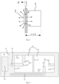
- an antenna assembly according to an embodiment of the present disclosure comprises a dielectric substrate 1, an antenna unit 2, a radio frequency chip 4 and a metal resonant cavity 3.
- the dielectric substrate 1 may be a PCB board of the antenna assembly
- the antenna unit 2 may be a unit that radiates electromagnetic waves
- the antenna unit 2 may be a metal sheet with a preset shape printed on the surface of the dielectric substrate 1, for example, a copper sheet with various shapes printed on the surface of the dielectric substrate 1.
- the antenna unit 2 includes a first antenna unit 21 and a second antenna unit 22.
- the first antenna unit 21 and the second antenna unit 22 can be electrically connected with the radio frequency chip 4 via a transmission line, for example, the first antenna unit 21 and the second antenna unit 22 can be electrically connected with the radio frequency chip 4 through a transmission line printed on the dielectric substrate 1.
- the metal resonant cavity 3 may be a cover made of metal materials such as stainless steel, galvanized steel plate, etc.
- the metal resonant cavity 3 is provided with an opening.
- the metal resonant cavity 3 may be a cover structure.
- the cover structure includes a bottom surface and a side surface connected with the bottom surface. The bottom surface and the side surfaces form a cover with an opening, preferably, a rectangular metal resonant cavity, which facilitates manufacturing the metal resonant cavity.
- a surface B in Fig. 4 is a first surface of the dielectric substrate 1.
- the first surface B may be provided with a ground plane 11 and a closed clearance region 12 located in the ground plane 11.
- the clearance region 12 may be a region in the ground plane 11 where ground plane has been partially removed, and the clearance region 12 may be a closed clearance region.
- the first antenna unit 21 and the second antenna unit 22 are spaced apart in the clearance region, which can improve a radiation efficiency of the antenna unit, and can be simplified to reduce an area of the antenna unit occupying the dielectric substrate 1, so that the entire antenna assembly can be made smaller.
- the first antenna unit 21 and the second antenna unit 22 are orthogonal.
- the first antenna unit 21 and the second antenna unit 22 being orthogonal means that a phase difference between a phase of the electromagnetic wave radiated by the first antenna unit 21 and a phase of the electromagnetic wave radiated by the second antenna unit 22 is 90°, so as to improve an isolation between the first antenna unit 21 and the second antenna unit 22 and improve the radiation performance of the antenna assembly.
- a surface A in Fig. 2 is a second surface A of the dielectric substrate 1, and the second surface A is provided with the metal resonant cavity 3.
- the first surface B and the second surface A of the dielectric substrate 1 are two surfaces of the dielectric substrate 1 used for arranging electrical components, that is, they are two surfaces on different sides of a main body of the dielectric substrate 1.
- the first antenna unit 21 and the second antenna unit 22 can radiate electromagnetic waves in all directions.
- the entire antenna assembly is finally required that a side (side F in Fig. 3 ), which is provided with the first antenna unit 21 and the second antenna unit 22, of the dielectric substrate 1 radiates electromagnetic waves (directions of multiple arrow on side F in Fig. 3 are radiation directions).
- the metal resonant cavity 3 may be arranged on a surface of the dielectric substrate 1 facing away from the first antenna unit 21 and the second antenna unit 22.
- the entire antenna assembly radiates electromagnetic waves only at the side F, and a directivity of the electromagnetic waves radiated by the antenna assembly is good.
- the electromagnetic waves radiated by the first antenna unit 21 and the second antenna unit 22 toward the metal resonant cavity 3 are reflected and then superimposed on electromagnetic waves radiated toward the side F, thereby enhancing the intensity of the electromagnetic wave radiated toward the side F.
- the metal resonant cavity 3 can also prevent the external electromagnetic wave from causing electromagnetic interference to the antenna unit 2, which improves an anti-electromagnetic interference performance of the antenna assembly.
- the projection of the clearance region 12 on the metal resonant cavity 3 is within the outer contour of the metal resonant cavity 3, so that all electromagnetic waves radiated by sides of the first antenna unit 21 and the second antenna unit 22 disposed in the clearance region 12 toward the metal resonant cavity 3 are reflected by an inner wall of the metal resonant cavity 3, which enhances the intensity of electromagnetic waves radiated toward the side F.
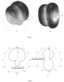
- Fig. 5 is a 3D schematic diagram of antenna radiation gain, wherein Fig. a in Fig. 5 is a 3D schematic diagram of radiation gain of the antenna after the metal resonant cavity 3 is added, and Fig. b in Fig. 5 is a 3D schematic diagram of radiation gain of the antenna before the metal resonant cavity 3 is added. It can be seen from Figs. a and b in Fig. 5 that in Fig. a, the radiation gain of the antenna after the metal resonant cavity 3 is added in Fig. 5 is concentrated in an upper region, the upper region is taken as a forward direction of the interactive white board, which can improve the forward radiation ability of the antenna assembly, and in Fig. b, the radiation gain of the antenna before the metal resonant cavity 3 is added is uniformly distributed in the upper and lower regions.
- Fig. 6 is a 2D schematic diagram of antenna radiation gain.
- Fig. a is a 2D schematic diagram of radiation gain of the antenna after the metal resonant cavity 3 is added
- Fig. b is a 2D schematic diagram of radiation gain of the antenna before the metal resonant cavity 3 is added. It can be seen from Figs. a and b in Fig. 6 that in Fig. a, the radiation gain of the antenna after the metal resonant cavity 3 is added reaches 3.1735dB, and in Fig. b, the radiation gain of the antenna before the metal resonant cavity 3 is added is 2.3983dB. That is, the radiation gain increases significantly after the metal resonant cavity 3 is added.
- the first surface of the dielectric substrate is provided with the ground plane and the closed clearance region located in the ground plane
- the first antenna unit and the second antenna unit are spaced apart on the first surface of the dielectric substrate and located in the clearance region
- the radio frequency chip is arranged on the dielectric substrate, and connected with the first antenna unit and the second antenna unit respectively
- the metal resonant cavity is arranged on the second surface of the dielectric substrate, and in the direction perpendicular to the second surface, at least a part of the projection of the clearance region on the metal resonant cavity is within an outer contour of the metal resonant cavity.
- the first surface, which is not provided with the metal resonant cavity, of the dielectric substrate in the antenna assembly faces the frame, so that the electromagnetic wave radiated by the antenna unit to the inside of the metal resonant cavity is reflected by the metal resonant cavity, and the reflected electromagnetic wave is radiated toward the direction of the first surface, and thus realizing that the antenna assembly radiates the electromagnetic wave to the side, which is provided with the first surface, of the dielectric substrate, and enhancing an intensity of the electromagnetic wave radiated from the side which is provided with the first surface.
- the first antenna unit and the second antenna unit are arranged orthogonally, and the isolation between the first antenna unit and the second antenna unit is high and the first antenna unit and the second antenna unit do not interfere with each other, thereby improving the radiation performance of the entire antenna assembly.
- the antenna unit is arranged in a closed clearance region, and thus wiring of the antenna unit can be simplified to reduce an area of the dielectric substrate, so that the antenna assembly can be made smaller.
- the radio frequency chip 4 may be arranged on a second surface A of the dielectric substrate 1, and the first antenna unit 21 and the second antenna unit 22 may be arranged on the first surface B of the dielectric substrate 1. Since the radio frequency chip 4 and the antenna unit 2 are located on two different surfaces of the dielectric substrate 1, the radio frequency chip 4 may connect with the first antenna unit 21 and the second antenna unit 22 through metal vias and transmission lines, so that the radio frequency chip 4, the first antenna unit 21 and the second antenna unit 22 can be arranged by making full use of the space on both sides of the dielectric substrate 1, thereby reducing the area of the dielectric substrate 1.
- the embodiment can be applied to the scene where the radio frequency chip 4, the first antenna unit 21 and the second antenna unit 22 cannot be arranged on the same surface of the dielectric substrate 1 due to the limited overall space of the interactive white board.
- the radio frequency chip 4 and the metal resonant cavity 3 are both arranged on the second surface A.
- the radio frequency chip 4 and the metal resonant cavity 3 can be simultaneously arranged on the second surface A of the dielectric substrate 1 through the SMT process, which eliminates the need for additional processes and reduces the manufacturing cost.
- the radio frequency chip 4 may also be arranged on the first surface B of the dielectric substrate 1, that is, the radio frequency chip 4, the first antenna unit 21 and the second antenna unit 22 are arranged on the same surface of the dielectric substrate 1, and pins of the radio frequency chip 4 can be directly connected with the transmission line without providing metal vias on the dielectric substrate 1, thereby reducing manufacturing cost of the dielectric substrate 1, and meanwhile being applied to the scene where the radio frequency chip 4, the first antenna unit 21 and the second antenna unit 22 are arranged on the same surface of the dielectric substrate 1 due to the limited overall space of the interactive white board.
- those skilled in the art can arrange the radio frequency chip 4, the first antenna unit 21 and the second antenna unit 22 on the same surface or on different surfaces according to actual needs, and the embodiments of the present disclosure are not limited thereto.
- the first antenna unit 21 and the second antenna unit 22 are electrically connected with the radio frequency chip 4 through a coplanar waveguide transmission line, and the coplanar waveguide transmission line may further be provided with an impedance matching circuit, for example, a ⁇ -shaped matching circuit.
- an impedance matching circuit for example, a ⁇ -shaped matching circuit.
- the metal resonant cavity 3 may be provided on the second surface A of the dielectric substrate 1 by welding, buckles, locking screws, etc.
- a contact surface between the metal resonant cavity 3 and the dielectric substrate 1 may also be provided with conductive fabric so as to improve the electromagnetic shielding performance of the metal resonant cavity 3.
- a distance from the bottom of the metal resonant cavity 3 to the antenna unit 2 is equal to one fourth of a wavelength of the electromagnetic wave radiated by the antenna unit 2.
- L ⁇ /4, wherein L is the distance from the bottom of the metal resonant cavity 3 to the antenna unit 2, and ⁇ is the wavelength of the electromagnetic wave.
- the distance from the bottom of the metal resonant cavity 3 to the antenna unit 2 is equal to one fourth of the wavelength of the electromagnetic wave radiated by the antenna unit 2
- the reflected electromagnetic wave and the electromagnetic wave radiated by the antenna unit 2 have a same phase.
- the superposition of the electromagnetic waves in the same phase can improve the signal intensity of the electromagnetic wave, and the forward radiation performance of the entire antenna assembly.
- the radio frequency chip 4 includes a first radio frequency chip 41, the clearance region 12 is provided with grounded stubs for increased isolation 13, the grounded stubs for increased isolation 13 divide the clearance region 12 into a closed first clearance region 121 and a closed second clearance region 122, the first antenna unit 21 is arranged in the first clearance region 121, and the second antenna unit 22 is arranged in the second clearance region 122.
- the first antenna unit 21 and the second antenna unit 22 are located on the same side of the first radio frequency chip 41, the first antenna unit 21 is located between the second antenna unit 22 and the first radio frequency chip 41, the first antenna unit 21 is connected with the first radio frequency chip 41 through the first coplanar waveguide transmission line 14, and the second antenna unit 22 is connected with the first radio frequency chip 41 through the second coplanar waveguide transmission line 15.
- the clearance region 12 is divided into a closed first clearance region 121 and a closed second clearance region 122 by the grounded stubs for increased isolation 13, so that the first antenna unit 21 located in the first clearance region 121 and the second antenna unit 22 located in the second clearance region 122 are isolated, thereby improving the isolation between the first antenna unit 21 and the second antenna unit 22.
- the interference between the first antenna unit 21 and the second antenna unit 22 is avoided, the anti-interference ability of the first antenna unit 21 and the second antenna unit 22 is improved, and the radiation performance of the antenna assembly is improved.
- the first radio frequency chip 41, the first antenna unit 21 and the second antenna unit 22 are arranged on the same surface of the dielectric substrate 1, the first radio frequency chip 41 can be directly connected with the first antenna unit 21 and the second antenna unit 22 through the coplanar waveguide transmission lines (14, 15).
- the first radio frequency chip 41, the first antenna unit 21 and the second antenna unit 22 are arranged on different surfaces of the dielectric substrate 1, after the coplanar waveguide transmission lines (14, 15) are connected with the first antenna unit 21 and the second antenna unit 22, the coplanar waveguide transmission lines (14, 15) are connected to the first radio frequency chip 41 on the other side through metal vias.
- the layout of the coplanar waveguide transmission lines (14, 15) on the dielectric substrate 1 can be determined according to the actual situation, and the embodiments of the present disclosure do not limit the wiring of the coplanar waveguide transmission lines (14, 15).
- the grounded stubs for increased isolation 13 divide the clearance region 12 into a closed first clearance region 121 and a closed second clearance region 122
- the first antenna unit 21 is arranged in the first clearance region 121
- the second antenna unit 22 is arranged in the second clearance region 122
- the projection of the first clearance region 121 or the second clearance region 122 on the metal resonant cavity 3 is within the outer contour of the metal resonant cavity 3, so that the electromagnetic wave radiated from the first antenna unit 21 or the second antenna unit 22 toward the metal resonant cavity 3 is reflected by the inner wall of the metal resonant cavity 3, thereby enhancing the intensity of the electromagnetic wave radiated toward the side F.
- the first clearance region 121 in the ground plane 11 is a square clearance region
- the first antenna unit 21 includes a first feeder stub 211 and a first ground stub 212
- the first feeder stub 211 extends from a first boundary 1211 of the first clearance region 121 to the inside of the first clearance region 121
- an end of the first feeder stub 211 close to the first boundary 2111 is connected with the first radio frequency chip 41 through the first coplanar waveguide transmission line 14.
- the first ground stub 212 extends from a second boundary 1212 of the first clearance region 121 to the inside of the first clearance region 121.
- the first boundary 1211 and the second boundary 1212 are two adjacent boundaries of the first clearance region 121.
- the first feeder stub 211 and the first ground stub 212 are arranged orthogonally and have no public endpoint.
- the first feeder stub 211 is perpendicular to the first boundary 1211.
- the orthogonal arrangement may mean that the first feeder stub 211 is perpendicular to the first ground stub 212.
- the second clearance region 122 is a square clearance region
- the second antenna unit 22 includes a second feeder stub 221 and a second ground stub 222.
- the second feeder stub 221 extends from a third boundary 1221 of the second clearance region 122 to the inside of the second clearance region 122.
- One end of the second feeder stub 221 close to the third boundary 1221 is connected with the first radio frequency chip 41 through the second coplanar waveguide transmission line 15.
- the second ground stub 222 extends from a fourth boundary 1222 of the second clearance region 122 to the inside of the second clearance region 122.
- the third boundary 1221 and the fourth boundary 1222 are two adjacent boundaries of the second clearance region 122.
- the second feeder stub 221 and the second ground stub 222 are arranged orthogonally and have no public endpoint.
- the second feeder stub 221 is perpendicular to the third boundary 1221.
- first boundary 1211 and the third boundary 1221 may be orthogonal or parallel.
- the first boundary 1211 and the third boundary 1221 are orthogonal, so that the radiation directions of the first antenna unit 21 and the second antenna unit 22 are orthogonal, the first antenna unit 21 and the second antenna unit 22 do not interfere with each other, and the degree of isolation is high.
- the first antenna unit 21 and the second antenna unit 22 respectively composes a feeder stub for feeder and a ground stub for ground, and the two stubs are placed orthogonally.
- the feeder stub is in the form of a monopole antenna. According to the antenna radiation principle, when a length of the feeder stub is about one fourth of the wavelength of the radiation frequency, the electric field intensity at the top of the feeder stub is the strongest.
- the ground stub after the ground stub is introduced at an orthogonal side of the feeder stub, the ground stub can be coupled with the feeder stub to change the radiation frequency, so that by adjusting the position and length of the ground stub, a current path length of the feeder stub can be effectively shortened by using the coupling effect, thereby reducing the size of the feeder stub.
- the size of the feeder stub shown in Fig. 4 is about one eighth of the wavelength of the radiation frequency, the size of the antenna unit is greatly reduced, so that the required clearance area of the antenna unit can be smaller, and the size of the antenna assembly can be made smaller.
- the antenna unit includes two stubs, and the structure is simple.
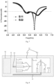
- Fig. 7 is a schematic diagram of the return loss of the antenna assembly in Fig. 4 . It can be seen from Fig. 7 that the return loss of the two antenna elements in Fig. 4 meets 5.15-5.85 GHz at an impedance bandwidth with less than -10 dB.
- first antenna unit 21 and the second antenna unit 22 have been exemplified with reference to Fig. 4 , in practical applications, those skilled in the art can also arrange the first antenna unit 21 and the second antenna unit 22 with any structure.
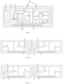
- the other two antenna units of the present disclosure will be described with reference to Figs. 8 and 9 .
- the first clearance region 121 is a square clearance region
- the first antenna unit 21 includes a first feeder stub 211, a first ground stub 212, and a third ground stub 213 arranged in parallel.
- the first feeder stub 211, the first ground stub 212, and the third ground stub 213 all extend from the first boundary 1211 of the first clearance region 121 to the inside of the first clearance region 121.
- One end of the first feeder stub 211 close to the first boundary 1211 is connected with the first clearance region chip 41 through the first coplanar waveguide transmission line 14.
- the first ground stub 212 and the third ground stub 213 are located on both sides of the first feeder stub 211, and the first feeder stub 211 is perpendicular to the first boundary 1211.
- the second clearance region 122 is a square clearance region
- the second antenna unit 22 includes a second feeder stub 221, a second ground stub 222 and a fourth ground stub 223 arranged in parallel.
- the second feeder stub 221, the second ground stub 222 and the fourth ground stub 223 all extend from the third boundary 1221 of the second clearance region 122 to the inside of the second headroom area 122.
- One end of the second feeder stub 221 close to the third boundary 1221 is connected with the first radio frequency chip 41 through the second coplanar waveguide transmission line 15.
- the second ground stub 222 and the fourth ground stub 223 are located on both sides of the second feeder stub 221.
- the second feeder stub 221 is perpendicular to the third boundary 1221. It should be noted that the first boundary 1211 and the third boundary 1221 may be orthogonal or parallel.
- the first clearance region 121 is a square clearance region
- the first antenna unit 21 includes a first feeder stub 211 and a first ground stub 212.
- the first feeder stub 211 extends from the first boundary 1211 of the first clearance region 121 to the inside of the first clearance region 121.
- One end of the first feeder stub 211 close to the first boundary 1211 is connected with the first radio frequency chip 41 through the first coplanar waveguide transmission line 14.
- the first ground stub 212 includes a first ground sub-stub 2121, a second ground sub-stub 2122, a third ground sub-stub 2123, and a fourth ground sub-stub 2124.
- the first ground sub-stub 2121 is parallel to the first feeder stub 211 and extends from the first boundary 1211 of the first clearance region 121 to the inside of the first clearance region 121.
- the second ground sub-stub 2122, the third ground sub-stub 2123, and the fourth ground sub-stub 2124 are connected end-to-end in sequence, and two adjacent ground sub-stubs are perpendicular to each other.
- One end, which is not connected with the third ground sub-stub 2123, of the second ground sub-stub 2122 is connected to one end, which is away from the first boundary 1211, of the first ground sub-stub 2121, and the second ground sub-stub 2122 is perpendicular to the first ground sub-stub 2121.
- One end, which is not connected with the third ground sub-stub 2123, of the fourth ground sub-stub 2124 is connected with the first feeder stub 211, and the first ground sub-stub 2121 and the third ground sub-stub 2123 are respectively located on both sides of the first feeder stub 211.
- the second clearance region 122 is a square clearance region
- the second antenna unit 22 includes a second feeder stub 221 and a second ground stub 222.
- the second feeder stub 221 extends from the third boundary 1221 of the second clearance region 122 to the inside of the second clearance region 122.
- One end of the second feeder stub 221 close to the third boundary 1221 is connected with the first radio frequency chip 41 through the second coplanar waveguide transmission line 15.
- the second ground stub 222 includes a fifth ground sub-stub 2221, a sixth ground sub-stub 2222, a seventh ground sub-stub 2223, and an eighth ground sub-stub 2224.
- the fifth ground sub-stub 2221 is parallel to the second feeder stub 221 and extends from the third boundary 1221 of the second clearance region 122 to the inside of the second clearance region 122.
- the sixth ground sub-stub 2222, the seventh ground sub-stub 2223, and the eighth ground sub-stub 2224 are connected end-to-end in sequence, and two adjacent ground sub-stubs are perpendicular to each other.
- One end, which is not connected with the seventh ground sub-stub 2223, of the sixth ground sub-stub 2222 is connected to one end, which is away from the third boundary 1221, of the fifth ground sub-stub 2221, and the sixth ground sub-stub 2222 is perpendicular to the fifth ground sub-stub 2221.
- One end, which is not connected with the seventh ground sub-stub 2223, of the eighth ground sub-stub 2224 is connected with the second feeder stub 221.
- the fifth ground sub-stub 2221 and the seventh ground sub-stub 2223 are respectively located on both sides of the second feeder stub 221. It should be noted that the first boundary 1211 and the third boundary 1221 may be orthogonal or parallel.
- the structure of the antenna unit 2 the structure and wiring of the transmission line have been described above by taking the example that the antenna unit 2 includes two antenna units and the transmission line is a coplanar waveguide transmission line, in practical applications, those skilled in the art can arrange the number of antenna units 2, design antenna units with different structures and transmission lines with different layouts according to actual needs, and the embodiments of the present disclosure do not limit the number and structure of antenna units, the structure and wiring mode of the transmission line are not limited.
- Fig. 10 is a schematic diagram of another antenna assembly in the example of the present disclosure.
- the antenna assembly in the embodiment of the present disclosure further includes a third antenna unit 23 and a fourth antenna unit 24, the radio frequency chip 4 further includes a second radio frequency chip 42, and the coplanar waveguide transmission line further includes a third coplanar waveguide transmission line 16 and a fourth coplanar waveguide transmission line 17.
- the second radio frequency chip 42 is located on a side of the first radio frequency chip 41 away from the first antenna unit 21
- the third antenna unit 23 and the fourth antenna unit 24 are located on a side of the second radio frequency chip 42 away from the first radio frequency chip 41
- the third antenna unit 23 is located between the second radio frequency chip 42 and the fourth antenna unit 24
- the third antenna unit 23 and the first antenna unit 21 are mirror images of each other
- the fourth antenna unit 24 and the second antenna unit 22 are mirror images of each other
- the third antenna unit 23 is connected with the second radio frequency chip 42 through the third coplanar waveguide transmission line 16
- the fourth antenna unit 24 is connected with the second radio frequency chip 42 through the fourth coplanar waveguide transmission line 17.
- being the mirror image of each other may mean that the third antenna unit 23 and the first antenna unit 21 are mirror images of each other in structure, the fourth antenna unit 24 and the second antenna unit 22 are mirror images of each other in structure.
- the structures of the third antenna unit 23 and the fourth antenna unit 24 may also be other structures, and the embodiments of the present disclosure are not limited thereto.
- the antenna assembly includes a first antenna unit 21, a second antenna unit 22, a third antenna unit 23, a fourth antenna unit 24, a first radio frequency chip 41, and a second radio frequency chip 42.
- the second radio frequency chip 42 is located on a side of the first radio frequency chip 41 away from the first antenna unit 21, the third antenna unit 23 and the fourth antenna unit 24 are located on a side of the second radio frequency chip 42 away from the first radio frequency chip 41, and the third antenna unit 23 is located between the second radio frequency chip 42 and the fourth antenna unit 24.
- the antenna assembly includes a first group of antennas units (the first antenna unit 21 and the second antenna unit 22) and a second group of antenna units (the third antenna unit 23 and the fourth antenna unit 24), and can realize different communication functions through the two groups of antennas.
- the antenna assembly can realize the WiFi communication functions through the first group of antennas units, and realize the wireless AP (Access Point) function through the second group of antenna units.
- there are two radio frequency chips (first radio frequency chip 41 and second radio frequency chip 42) between the first group of antennas units (the first antenna unit 21 and the second antenna unit 22) and the second group of antenna units (the third antenna unit 23 and the fourth antenna unit 24). The distance between the two groups of antennas is large, the isolation of the two groups of antennas is high, and the area of the entire antenna assembly is small.
- Fig. 11 is a schematic diagram of another antenna assembly according to an embodiment of the present disclosure.
- the antenna assembly of this embodiment in the present disclosure further includes the third antenna unit 23 and the fourth antenna unit 24, the radio frequency chip 4 further includes the second radio frequency chip 42, and the coplanar waveguide transmission line further includes the third coplanar waveguide transmission line 16 and the fourth coplanar waveguide transmission line 17.
- the second radio frequency chip 42 is located on a side of the first radio frequency chip 41 away from the first antenna unit 21, the third antenna unit 23 and the fourth antenna unit 24 are located between the second radio frequency chip 42 and the first radio frequency chip 41, the third antenna unit 23 has the same structure as the first antenna unit 21, the fourth antenna unit 24 has the same structure as the second antenna unit 22, the third antenna unit 23 is located between the second radio frequency chip 42 and the fourth antenna unit 24, the third antenna unit 23 is connected with the second radio frequency chip 42 through the third coplanar waveguide transmission line 16, and the fourth antenna unit 24 is connected with the second radio frequency chip 42 through the fourth coplanar waveguide transmission line 17.
- the structures of the third antenna unit 23 and the fourth antenna unit 24 may also be other structures, and the embodiments of the present disclosure are not limited thereto.
- the antenna assembly includes a first antenna unit 21, a second antenna unit 22, a third antenna unit 23, a fourth antenna unit 24, a first radio frequency chip 41 and a second radio frequency chip 42.
- the second radio frequency chip 42 is located on a side of the first radio frequency chip 41 away from the first antenna unit 21.
- the third antenna unit 23 and the fourth antenna unit 24 are located between the second radio frequency chip 42 and the first radio frequency chip 41.
- the antenna assembly includes a first group of antennas units (the first antenna unit 21 and the second antenna unit 22) and a second group of antenna units (the third antenna unit 23 and the fourth antenna unit 24), and can realize different communication functions through the two groups of antennas.
- the antenna assembly can realize the WiFi communication function through the first group of antennas units, and realize the wireless AP (Access Point) function through the second group of antenna units.
- the isolation of the two groups of antennas can be improved by increasing the distance between the first group of antennas units (the first antenna unit 21 and the second antenna unit 22) and the second group of antenna units (the third antenna unit 23 and the fourth antenna unit 24).
- the increase of the area of the dielectric substrate is suitable for scenes where the installation space of the antenna components is not limited.
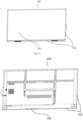
- the embodiment of the present disclosure provides an interactive white board 100
- the interactive white board 100 includes a display screen 101, a frame 102 arranged around the display screen 101, and at least one antenna assembly 103 provided in the embodiment of the present disclosure.
- the antenna assembly 103 is located in the interactive white board 100 and connected to the frame 102, wherein a surface, which is not provided with a metal resonant cavity, of the dielectric substrate in the antenna assembly 103 faces the frame 102. That is, the antenna assembly 103 radiates electromagnetic waves to the outside of the interactive white board 100.
- the display screen 101 may be one of display screen selected from the group consisting of LCD, LED, OLED, etc.
- the frame 102 may be a frame surrounding the display screen 101.
- the frame 102 has a certain thickness in the direction perpendicular to the display screen 101, so that the antenna assembly 103 may be mounted on the frame 102.
- the number of antenna assemblies 103 may be one or more.
- the first surface of the dielectric substrate is provided with a ground plane and a closed clearance area located in the ground plane
- the antenna unit is arranged on the first surface of the dielectric substrate and is located in the clearance area
- the radio frequency chip is provided on the dielectric substrate and connected with the antenna unit
- the metal resonant cavity is provided on the second surface of the dielectric substrate
- the projection of the metal resonant cavity on the first surface covers the antenna unit.
- the first surface, which is not provided with the metal resonant cavity, of the dielectric substrate in the antenna assembly faces the frame, so that the electromagnetic wave radiated by the antenna unit to the inside of the metal resonant cavity is reflected by the metal resonant cavity, and the reflected electromagnetic wave is radiated toward the first surface. Therefore, the antenna assembly radiates electromagnetic waves to the side of the dielectric substrate which is provided with the first surface, and the intensity of electromagnetic waves radiated from the surface of the dielectric substrate which is provided with the first surface is enhanced.
- the antenna unit is arranged in a closed clearance area, and wiring of the antenna unit can be simplified so as to reduce the area of the dielectric substrate, and thus the antenna assembly can be made smaller and the frame of the interactive white board can be made narrower.
- the number of antenna units in the antenna assembly may be one or more, the antenna unit and the radio frequency chip may be arranged on the same or different surfaces of the dielectric substrate, and the interactive white board may select the antenna assembly according to the installation space, radiation performance and radiation direction of the antenna assembly.
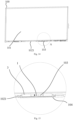
- the frame 102 of the interactive white board 100 includes a lower frame 1021, and the antenna assembly 103 is detachably connected with the lower frame 1021.
- One surface, which is provided with the metal resonant cavity 3, of the dielectric substrate 1 in the antenna assembly 103 faces a bottom surface 10212 of the lower frame 1021, and the bottom surface 10212 is substantially perpendicular to the display screen 101.
- the bottom surface 10212 of the lower frame 1021 may be a surface substantially parallel to the horizontal plane.
- the material of the lower frame 1021 may be metal, and the bottom surface 10212 of the lower frame 1021 is provided with an avoidance hole 10211 directly facing the antenna assembly 103, so that after the antenna assembly 103 is mounted on the lower frame 1021, the surface, which is not provided with the metal resonant cavity 3, of the dielectric substrate 1 in the antenna assembly 103 directly faces the avoidance hole 10211, and the antenna unit on the antenna assembly 103 can radiate electromagnetic waves to the outside of the interactive white board 100 through the avoidance hole 10211.
- the surface, which is not provided with the metal resonant cavity 3, of the dielectric substrate 1 in the antenna assembly 103 is arranged toward the bottom surface 10212 of the lower frame 1021. A surface of the lower frame 1021 facing the user does not need to be provided with an avoidance hole, so that the interactive white board has a good appearance.
- the surface, which is not provided with the metal resonant cavity 3, of the dielectric substrate 1 in the antenna assembly 103 faces a side surface 10213 of the lower frame 1021, wherein the side surface 10213 is parallel to the display screen 101.
- the side surface 10213 of the lower frame 1021 may be a plane substantially perpendicular to the horizontal plane, for example, the side surface 10213 of the lower frame 1021 may be a surface facing the forward direction of the interactive white board, so that the antenna assembly 103 radiates electromagnetic waves directly toward the forward direction of the interactive white board.
- the antenna assembly 103 may also be mounted on other frames of the interactive white board 100.
- the antenna assembly 103 can be mounted on the left frame or the right frame.
- the surface, which is not provided with the metal resonant cavity 3, of the dielectric substrate 1 in the antenna assembly 103 can also be in the same direction as the front of the display screen 101.
- the embodiment of the present disclosure does not limit the mounting position and orientation of the antenna assembly 103.
- the antenna assembly according to the embodiment of the present disclosure is located at the lower frame of the interactive white board.
- the surface, which is not provided with a metal resonant, of the dielectric substrate 1 in the antenna assembly faces the bottom surface of the lower frame.
- the lower frame has sufficient installation space, which can facilitate the installation of the antenna assembly.
- the lower frame of the interactive white board is closer to the user, and the antenna assembly being located at the lower frame improves a wide radiation area, which improves the wireless network performance of the interactive white board.
- the interactive white board 100 further includes a decorative piece 104, which covers the avoidance hole 10211 so as to prevent the avoidance hole 10211 from directly exposing the dielectric substrate 1 of the antenna assembly 103, so that the interactive white board 100 has a good appearance.
- a decorative piece 104 which covers the avoidance hole 10211 so as to prevent the avoidance hole 10211 from directly exposing the dielectric substrate 1 of the antenna assembly 103, so that the interactive white board 100 has a good appearance.
Landscapes
- Engineering & Computer Science (AREA)
- Computer Networks & Wireless Communication (AREA)
- Computer Hardware Design (AREA)
- General Engineering & Computer Science (AREA)
- Physics & Mathematics (AREA)
- Electromagnetism (AREA)
- Details Of Aerials (AREA)
- Waveguide Aerials (AREA)
- Support Of Aerials (AREA)
- Variable-Direction Aerials And Aerial Arrays (AREA)
Abstract
Description
- The present disclosure relates to the technical field of antennas, and in particular to an antenna assembly and an interactive white board.
- With progress of wireless communication technology, a wireless communication technology has been applied in an interactive white board, and the wireless data transmission function in the interactive white board needs the support of antennas.
- In the interactive white board, wireless access point function and connection to a screen transmitter are realized through an antenna. A user of the wireless access point function and the screen transmitter are usually in front of the interactive white board. The users in front of the interactive white board can access a network through the wireless access point function of the interactive white board, and the data on PC can be transmitted to the interactive white board through the screen transmitter for display.
- At present, the antenna in the interactive white board is omnidirectional radiation, and a forward radiation performance of the antenna is poor. In order to improve the forward radiation performance, a complex antenna is arranged, resulting in an increase in the volume of the entire antenna.
- The purpose of embodiments of the present disclosure is to provide an antenna assembly and an interactive white board in order to solve problems of omnidirectional radiation, poor forward radiation performance and large volume of the antenna in the interactive white board.
- In order to achieve this purpose, the embodiments of the present disclosure adopt the following technical scheme:
- A first aspect provides an antenna assembly, comprising:
- a dielectric substrate, of which a first surface is provided with a ground plane and a closed clearance region located in the ground plane;
- a first antenna unit and a second antenna unit, the first antenna unit and the second antenna unit being spaced apart on the first surface of the dielectric substrate and located in the clearance region, and the first antenna unit and the second antenna unit being orthogonally arranged;
- a radio frequency chip, arranged on the dielectric substrate and connected with the first antenna unit and the second antenna unit respectively; and
- a metal resonant cavity arranged on a second surface of the dielectric substrate, wherein in a direction perpendicular to the second surface, at least a part of a projection of the clearance region on the metal resonant cavity is within an outer contour of the metal resonant cavity.
- In a second aspect, embodiments of the present disclosure provide an interactive white board. The interactive white board comprises a display screen, a frame arranged around the display screen, and an antenna assembly according to the first aspect, wherein the antenna assembly is located in the interactive white board and connected with the frame, and a surface, which is not provided with the metal resonant cavity, of the dielectric substrate in the antenna assembly faces the frame.
- In the antenna assembly according to embodiments of the present disclosure, the first surface of the dielectric substrate is provided with the ground plane and the closed clearance region located in the ground plane, the first antenna unit and the second antenna unit are spaced apart on the first surface of the dielectric substrate and located in the clearance region. The radio frequency chip is arranged on the dielectric substrate, and connected with the first antenna unit and the second antenna unit respectively. The metal resonant cavity is arranged on the second surface of the dielectric substrate. In the direction perpendicular to the second surface, at least a part of the projection of the clearance region on the metal resonant cavity is within an outer contour of the metal resonant cavity. When the antenna assembly is installed on the interactive white board, the antenna assembly can be located in the interactive white board and connected with the frame, and the first surface, which is not provided with the metal resonant cavity, of the dielectric substrate in the antenna assembly faces the frame, so that the electromagnetic wave radiated from the antenna unit in the clearance region to the inside of the metal resonant cavity is reflected by the metal resonant cavity, and the reflected electromagnetic wave is radiated toward the direction of the first surface, thereby realizing that the antenna assembly radiates the electromagnetic wave to the side, which is provided with the first surface, of the dielectric substrate, and enhancing an intensity of the electromagnetic wave radiated from the side provided with the first surface. Moreover, the first antenna unit and the second antenna unit are arranged orthogonally, the isolation between the first antenna unit and the second antenna unit is high, and the first antenna unit and the second antenna unit does not interfere with each other, thereby improving the radiation performance of the entire antenna assembly. In addition, the antenna unit is arranged in a closed clearance region, and thus wiring of the antenna unit can be simplified to reduce an area of the dielectric substrate, so that the antenna assembly can be made smaller.
- The present disclosure will be further described in detail according to the drawings and embodiments.
-
Fig. 1 is a schematic diagram of an overall structure of an antenna assembly according to an embodiment of the present disclosure. -
Fig. 2 is a schematic diagram of an exploded structure of an antenna assembly according to the embodiment of the present disclosure. -
Fig. 3 is a schematic diagram of a direction of electromagnetic waves radiated by the antenna assembly in the embodiment of the present disclosure. -
Fig. 4 is a schematic diagram of a structure of an antenna unit according to the embodiment of the present disclosure. -
Fig. 5 is a 3D schematic diagram of radiation gain of the antenna assembly before and after the metal resonant cavity is added according to the embodiment of the present disclosure. -
Fig. 6 is a 2D schematic diagram of radiation gain of the antenna assembly before and after the metal resonant cavity is added according to the embodiment of the present disclosure. -
Fig. 7 is a schematic diagram of a return loss of the antenna assembly inFig. 4 . -
Fig. 8 is a schematic diagram of a structure of an antenna unit according to another embodiment of the present disclosure. -
Fig. 9 is a schematic diagram of a structure of an antenna unit according to another embodiment of the present disclosure. -
Fig. 10 is a schematic diagram of a layout of an antenna unit in an antenna assembly according to another embodiment of the present disclosure. -
Fig. 11 is a schematic diagram of a layout of an antenna unit in an antenna assembly according to another embodiment of the present disclosure. -
Fig. 12 is a schematic diagram of a front structure of the interactive white board according to the present disclosure. -
Fig. 13 is a schematic diagram of a back structure of the interactive white board according to the present disclosure. -
Fig. 14 is a partial exploded schematic diagram of an installation position of the antenna assembly according to the embodiment of the present disclosure. -
Fig. 15 is an enlarged schematic diagram of part A inFig. 14 . -
Fig. 16 is a schematic diagram of an avoidance hole of a lower frame in the part A inFig. 14 . -
Fig. 17 is a schematic diagram of the location of the antenna assembly and the lower frame. - In the figures,
1. Dielectric substrate; 11. Ground plane; 12. Clearance region; 121. First clearance region; 1211. First boundary; 1212. Second boundary; 122. Second clearance region; 1221. Third boundary; 1222. Fourth boundary; 13. Grounded stubs for increased isolation; 14. First coplanar waveguide transmission line; 15. Second coplanar waveguide transmission line; 16. Third coplanar waveguide transmission line; 17. Fourth coplanar waveguide transmission line; 2. Antenna unit; 21. First antenna unit; 211. First feeder stub; 212. First ground stub; 2121. First ground sub-stub; 2122. Second ground sub-stub; 2123. Third ground sub-stub; 2124. Fourth ground sub-stub; 213. Third ground stub; 22. Second antenna unit; 221. Second feeder stub; 222. Second ground stub; 2221. Fifth ground sub-stub; 2222. Sixth ground sub-stub; 2223. Seventh ground sub-stub; 2124. Eighth ground sub-stub; 223. Fourth ground stub; 23. Third antenna unit; 24. Fourth antenna unit; 3. Metal resonant cavity; 4. Radio frequency chip; 41. First radio frequency chip; 42. Second radio frequency chip; 100. Interactive white board; 101. Display screen; 102. Frame; 1021. Lower frame; 10211. Avoidance hole; 10212. Bottom surface; 10213. Side surface; 103. Antenna assembly; 104. Decorative piece. - In order to make the technical problems to be solved, the technical solutions to be adopted and the technical effects to be achieved by the present disclosure more clear, the technical solutions of embodiments of the present disclosure will be further described in detail hereinafter in combination with the accompanying drawings. Obviously, the described embodiments are only a part of embodiments of the present disclosure, not all of embodiments of the present disclosure. Based on the embodiments of the present disclosure, all other embodiments obtained by those skilled in the art without creative work belong to the claimed scope of the present disclosure.
- In the description of the present disclosure, unless otherwise specified and limited, the terms "connected with/to", "connected" and "fixed" should be interpreted broadly. For example, they can be fixedly connected, detachably connected, or integrated. It can be a mechanical connection or an electrical connection. And they can be directly connected or indirectly connected through an intermediate medium, or, they can be the connection between two components or the interaction relationship between two components. For those skilled in the art, the concrete meaning of the above-mentioned terms in the present disclosure can be understood under concrete circumstances.
- In the present disclosure, unless expressly stipulated and defined otherwise, a first feature being "above" or "below" a second feature may comprise that the first feature directly contacts with the second feature, or may comprise that the first feature does not directly contact with the second feature, rather than contact through another feature therebetween. Moreover, the first feature being "above", "over" and "on" the second feature may comprise that the first feature is directly above and obliquely above the second feature, or simply means that the level of the first feature is higher than that of the second feature. The first feature being "below", "under" and "underneath" the second feature comprises that the first feature is directly below and obliquely below the second feature, or simply means that the level of the first feature is smaller than that of the second feature.
- As shown in
Figs. 1 and 2 , an antenna assembly according to an embodiment of the present disclosure comprises a dielectric substrate 1, anantenna unit 2, aradio frequency chip 4 and a metalresonant cavity 3. - Therein, the dielectric substrate 1 may be a PCB board of the antenna assembly, the
antenna unit 2 may be a unit that radiates electromagnetic waves, and theantenna unit 2 may be a metal sheet with a preset shape printed on the surface of the dielectric substrate 1, for example, a copper sheet with various shapes printed on the surface of the dielectric substrate 1. Therein, theantenna unit 2 includes afirst antenna unit 21 and asecond antenna unit 22. Thefirst antenna unit 21 and thesecond antenna unit 22 can be electrically connected with theradio frequency chip 4 via a transmission line, for example, thefirst antenna unit 21 and thesecond antenna unit 22 can be electrically connected with theradio frequency chip 4 through a transmission line printed on the dielectric substrate 1. - The metal
resonant cavity 3 may be a cover made of metal materials such as stainless steel, galvanized steel plate, etc. The metalresonant cavity 3 is provided with an opening. Specifically, the metalresonant cavity 3 may be a cover structure. The cover structure includes a bottom surface and a side surface connected with the bottom surface. The bottom surface and the side surfaces form a cover with an opening, preferably, a rectangular metal resonant cavity, which facilitates manufacturing the metal resonant cavity. - As shown in
Figs. 2 and4 , a surface B inFig. 4 is a first surface of the dielectric substrate 1. The first surface B may be provided with aground plane 11 and aclosed clearance region 12 located in theground plane 11. Therein, theclearance region 12 may be a region in theground plane 11 where ground plane has been partially removed, and theclearance region 12 may be a closed clearance region. Thefirst antenna unit 21 and thesecond antenna unit 22 are spaced apart in the clearance region, which can improve a radiation efficiency of the antenna unit, and can be simplified to reduce an area of the antenna unit occupying the dielectric substrate 1, so that the entire antenna assembly can be made smaller. In addition, thefirst antenna unit 21 and thesecond antenna unit 22 are orthogonal. Thefirst antenna unit 21 and thesecond antenna unit 22 being orthogonal means that a phase difference between a phase of the electromagnetic wave radiated by thefirst antenna unit 21 and a phase of the electromagnetic wave radiated by thesecond antenna unit 22 is 90°, so as to improve an isolation between thefirst antenna unit 21 and thesecond antenna unit 22 and improve the radiation performance of the antenna assembly. - A surface A in
Fig. 2 is a second surface A of the dielectric substrate 1, and the second surface A is provided with the metalresonant cavity 3. In a direction perpendicular to the second surface A, at least a part of a projection of theclearance region 12 on the metalresonant cavity 3 is within an outer contour of the metalresonant cavity 3. It should be noted that the first surface B and the second surface A of the dielectric substrate 1 are two surfaces of the dielectric substrate 1 used for arranging electrical components, that is, they are two surfaces on different sides of a main body of the dielectric substrate 1. - As shown in
Fig. 3 , in the embodiment of the present disclosure, thefirst antenna unit 21 and thesecond antenna unit 22 can radiate electromagnetic waves in all directions. The entire antenna assembly is finally required that a side (side F inFig. 3 ), which is provided with thefirst antenna unit 21 and thesecond antenna unit 22, of the dielectric substrate 1 radiates electromagnetic waves (directions of multiple arrow on side F inFig. 3 are radiation directions). As shown inFig. 3 , the metalresonant cavity 3 may be arranged on a surface of the dielectric substrate 1 facing away from thefirst antenna unit 21 and thesecond antenna unit 22. Moreover, since at least a part of the projection of theclearance region 12 on the metalresonant cavity 3 is within the outer contour of the metalresonant cavity 3, at least a part of the electromagnetic waves radiated by thefirst antenna unit 21 and thesecond antenna unit 22 arranged in theclearance region 12 toward the metalresonant cavity 3 are reflected by an inner wall of the metalresonant cavity 3. The reflected electromagnetic wave is radiated to a side (side F inFig. 3 ), which is provided with thefirst antenna unit 21 and thesecond antenna unit 22, of the dielectric substrate 1. On the one hand, the entire antenna assembly radiates electromagnetic waves only at the side F, and a directivity of the electromagnetic waves radiated by the antenna assembly is good. On the other hand, the electromagnetic waves radiated by thefirst antenna unit 21 and thesecond antenna unit 22 toward the metalresonant cavity 3 are reflected and then superimposed on electromagnetic waves radiated toward the side F, thereby enhancing the intensity of the electromagnetic wave radiated toward the side F. On the other hand, the metalresonant cavity 3 can also prevent the external electromagnetic wave from causing electromagnetic interference to theantenna unit 2, which improves an anti-electromagnetic interference performance of the antenna assembly. - In a preferred embodiment, the projection of the
clearance region 12 on the metalresonant cavity 3 is within the outer contour of the metalresonant cavity 3, so that all electromagnetic waves radiated by sides of thefirst antenna unit 21 and thesecond antenna unit 22 disposed in theclearance region 12 toward the metalresonant cavity 3 are reflected by an inner wall of the metalresonant cavity 3, which enhances the intensity of electromagnetic waves radiated toward the side F. -
Fig. 5 is a 3D schematic diagram of antenna radiation gain, wherein Fig. a inFig. 5 is a 3D schematic diagram of radiation gain of the antenna after the metalresonant cavity 3 is added, and Fig. b inFig. 5 is a 3D schematic diagram of radiation gain of the antenna before the metalresonant cavity 3 is added. It can be seen from Figs. a and b inFig. 5 that in Fig. a, the radiation gain of the antenna after the metalresonant cavity 3 is added inFig. 5 is concentrated in an upper region, the upper region is taken as a forward direction of the interactive white board, which can improve the forward radiation ability of the antenna assembly, and in Fig. b, the radiation gain of the antenna before the metalresonant cavity 3 is added is uniformly distributed in the upper and lower regions. -
Fig. 6 is a 2D schematic diagram of antenna radiation gain. Therein, inFig. 6 , Fig. a is a 2D schematic diagram of radiation gain of the antenna after the metalresonant cavity 3 is added, and Fig. b is a 2D schematic diagram of radiation gain of the antenna before the metalresonant cavity 3 is added. It can be seen from Figs. a and b inFig. 6 that in Fig. a, the radiation gain of the antenna after the metalresonant cavity 3 is added reaches 3.1735dB, and in Fig. b, the radiation gain of the antenna before the metalresonant cavity 3 is added is 2.3983dB. That is, the radiation gain increases significantly after the metalresonant cavity 3 is added. - In the antenna assembly according to this embodiment of the present disclosure, the first surface of the dielectric substrate is provided with the ground plane and the closed clearance region located in the ground plane, the first antenna unit and the second antenna unit are spaced apart on the first surface of the dielectric substrate and located in the clearance region, the radio frequency chip is arranged on the dielectric substrate, and connected with the first antenna unit and the second antenna unit respectively, the metal resonant cavity is arranged on the second surface of the dielectric substrate, and in the direction perpendicular to the second surface, at least a part of the projection of the clearance region on the metal resonant cavity is within an outer contour of the metal resonant cavity. When the antenna assembly is installed on the interactive white board, the antenna assembly can be located in the interactive white board and connected with the frame. The first surface, which is not provided with the metal resonant cavity, of the dielectric substrate in the antenna assembly faces the frame, so that the electromagnetic wave radiated by the antenna unit to the inside of the metal resonant cavity is reflected by the metal resonant cavity, and the reflected electromagnetic wave is radiated toward the direction of the first surface, and thus realizing that the antenna assembly radiates the electromagnetic wave to the side, which is provided with the first surface, of the dielectric substrate, and enhancing an intensity of the electromagnetic wave radiated from the side which is provided with the first surface. Moreover, the first antenna unit and the second antenna unit are arranged orthogonally, and the isolation between the first antenna unit and the second antenna unit is high and the first antenna unit and the second antenna unit do not interfere with each other, thereby improving the radiation performance of the entire antenna assembly. In addition, the antenna unit is arranged in a closed clearance region, and thus wiring of the antenna unit can be simplified to reduce an area of the dielectric substrate, so that the antenna assembly can be made smaller.
- In an optional embodiment of the present disclosure, the
radio frequency chip 4 may be arranged on a second surface A of the dielectric substrate 1, and thefirst antenna unit 21 and thesecond antenna unit 22 may be arranged on the first surface B of the dielectric substrate 1. Since theradio frequency chip 4 and theantenna unit 2 are located on two different surfaces of the dielectric substrate 1, theradio frequency chip 4 may connect with thefirst antenna unit 21 and thesecond antenna unit 22 through metal vias and transmission lines, so that theradio frequency chip 4, thefirst antenna unit 21 and thesecond antenna unit 22 can be arranged by making full use of the space on both sides of the dielectric substrate 1, thereby reducing the area of the dielectric substrate 1. Therefore, the embodiment can be applied to the scene where theradio frequency chip 4, thefirst antenna unit 21 and thesecond antenna unit 22 cannot be arranged on the same surface of the dielectric substrate 1 due to the limited overall space of the interactive white board. In addition, theradio frequency chip 4 and the metalresonant cavity 3 are both arranged on the second surface A. During production and manufacture, theradio frequency chip 4 and the metalresonant cavity 3 can be simultaneously arranged on the second surface A of the dielectric substrate 1 through the SMT process, which eliminates the need for additional processes and reduces the manufacturing cost. - Definitely, the
radio frequency chip 4 may also be arranged on the first surface B of the dielectric substrate 1, that is, theradio frequency chip 4, thefirst antenna unit 21 and thesecond antenna unit 22 are arranged on the same surface of the dielectric substrate 1, and pins of theradio frequency chip 4 can be directly connected with the transmission line without providing metal vias on the dielectric substrate 1, thereby reducing manufacturing cost of the dielectric substrate 1, and meanwhile being applied to the scene where theradio frequency chip 4, thefirst antenna unit 21 and thesecond antenna unit 22 are arranged on the same surface of the dielectric substrate 1 due to the limited overall space of the interactive white board. In practical application, those skilled in the art can arrange theradio frequency chip 4, thefirst antenna unit 21 and thesecond antenna unit 22 on the same surface or on different surfaces according to actual needs, and the embodiments of the present disclosure are not limited thereto. - In another embodiment of the present disclosure, the
first antenna unit 21 and thesecond antenna unit 22 are electrically connected with theradio frequency chip 4 through a coplanar waveguide transmission line, and the coplanar waveguide transmission line may further be provided with an impedance matching circuit, for example, a π-shaped matching circuit. By arranging the impedance matching circuit, the frequency of the antenna assembly can be adjusted after a frequency offset of the antenna assembly, and the antenna assembly can be matched with an active device so as to improve the overall radiation performance of the antenna assembly. - In practical applications, the metal
resonant cavity 3 may be provided on the second surface A of the dielectric substrate 1 by welding, buckles, locking screws, etc. Optionally, a contact surface between the metalresonant cavity 3 and the dielectric substrate 1 may also be provided with conductive fabric so as to improve the electromagnetic shielding performance of the metalresonant cavity 3. - In a preferred embodiment, a distance from the bottom of the metal
resonant cavity 3 to theantenna unit 2 is equal to one fourth of a wavelength of the electromagnetic wave radiated by theantenna unit 2. As shown inFig. 3 , L=λ/4, wherein L is the distance from the bottom of the metalresonant cavity 3 to theantenna unit 2, and λ is the wavelength of the electromagnetic wave. By setting the distance from the bottom of the metalresonant cavity 3 to theantenna unit 2 to be equal to one fourth of the wavelength of the electromagnetic wave radiated by theantenna unit 2, when the electromagnetic wave radiated by theantenna unit 2 to the bottom of the metalresonant cavity 3 reaches theantenna unit 2 through reflection, the reflected electromagnetic wave and the electromagnetic wave radiated by theantenna unit 2 have a same phase. The superposition of the electromagnetic waves in the same phase can improve the signal intensity of the electromagnetic wave, and the forward radiation performance of the entire antenna assembly. - As shown in
Fig. 4 , in an optional embodiment of the present disclosure, theradio frequency chip 4 includes a firstradio frequency chip 41, theclearance region 12 is provided with grounded stubs for increasedisolation 13, the grounded stubs for increasedisolation 13 divide theclearance region 12 into a closedfirst clearance region 121 and a closedsecond clearance region 122, thefirst antenna unit 21 is arranged in thefirst clearance region 121, and thesecond antenna unit 22 is arranged in thesecond clearance region 122. Specifically, thefirst antenna unit 21 and thesecond antenna unit 22 are located on the same side of the firstradio frequency chip 41, thefirst antenna unit 21 is located between thesecond antenna unit 22 and the firstradio frequency chip 41, thefirst antenna unit 21 is connected with the firstradio frequency chip 41 through the first coplanarwaveguide transmission line 14, and thesecond antenna unit 22 is connected with the firstradio frequency chip 41 through the second coplanarwaveguide transmission line 15. - When the
antenna unit 2 according to the embodiment of the present disclosure includes thefirst antenna unit 21 and thesecond antenna unit 22, theclearance region 12 is divided into a closedfirst clearance region 121 and a closedsecond clearance region 122 by the grounded stubs for increasedisolation 13, so that thefirst antenna unit 21 located in thefirst clearance region 121 and thesecond antenna unit 22 located in thesecond clearance region 122 are isolated, thereby improving the isolation between thefirst antenna unit 21 and thesecond antenna unit 22. Thus, the interference between thefirst antenna unit 21 and thesecond antenna unit 22 is avoided, the anti-interference ability of thefirst antenna unit 21 and thesecond antenna unit 22 is improved, and the radiation performance of the antenna assembly is improved. - It should be noted that when the first
radio frequency chip 41, thefirst antenna unit 21 and thesecond antenna unit 22 are arranged on the same surface of the dielectric substrate 1, the firstradio frequency chip 41 can be directly connected with thefirst antenna unit 21 and thesecond antenna unit 22 through the coplanar waveguide transmission lines (14, 15). When the firstradio frequency chip 41, thefirst antenna unit 21 and thesecond antenna unit 22 are arranged on different surfaces of the dielectric substrate 1, after the coplanar waveguide transmission lines (14, 15) are connected with thefirst antenna unit 21 and thesecond antenna unit 22, the coplanar waveguide transmission lines (14, 15) are connected to the firstradio frequency chip 41 on the other side through metal vias. Therein, the layout of the coplanar waveguide transmission lines (14, 15) on the dielectric substrate 1 can be determined according to the actual situation, and the embodiments of the present disclosure do not limit the wiring of the coplanar waveguide transmission lines (14, 15). - In an optional embodiment, when the grounded stubs for increased
isolation 13 divide theclearance region 12 into a closedfirst clearance region 121 and a closedsecond clearance region 122, thefirst antenna unit 21 is arranged in thefirst clearance region 121, and thesecond antenna unit 22 is arranged in thesecond clearance region 122, the projection of thefirst clearance region 121 or thesecond clearance region 122 on the metalresonant cavity 3 is within the outer contour of the metalresonant cavity 3, so that the electromagnetic wave radiated from thefirst antenna unit 21 or thesecond antenna unit 22 toward the metalresonant cavity 3 is reflected by the inner wall of the metalresonant cavity 3, thereby enhancing the intensity of the electromagnetic wave radiated toward the side F. - In order to enable those skilled in the art to understand the antenna assembly of the embodiment of the present disclosure more clearly, the antenna assembly of the embodiment of the present disclosure will be described hereinafter with reference to
Fig. 4 . - As shown in
Fig. 4 , thefirst clearance region 121 in theground plane 11 is a square clearance region, thefirst antenna unit 21 includes afirst feeder stub 211 and afirst ground stub 212, thefirst feeder stub 211 extends from afirst boundary 1211 of thefirst clearance region 121 to the inside of thefirst clearance region 121, and an end of thefirst feeder stub 211 close to the first boundary 2111 is connected with the firstradio frequency chip 41 through the first coplanarwaveguide transmission line 14. Thefirst ground stub 212 extends from asecond boundary 1212 of thefirst clearance region 121 to the inside of thefirst clearance region 121. Thefirst boundary 1211 and thesecond boundary 1212 are two adjacent boundaries of thefirst clearance region 121. Thefirst feeder stub 211 and thefirst ground stub 212 are arranged orthogonally and have no public endpoint. Thefirst feeder stub 211 is perpendicular to thefirst boundary 1211. Therein, the orthogonal arrangement may mean that thefirst feeder stub 211 is perpendicular to thefirst ground stub 212. - The
second clearance region 122 is a square clearance region, and thesecond antenna unit 22 includes asecond feeder stub 221 and asecond ground stub 222. Thesecond feeder stub 221 extends from athird boundary 1221 of thesecond clearance region 122 to the inside of thesecond clearance region 122. One end of thesecond feeder stub 221 close to thethird boundary 1221 is connected with the firstradio frequency chip 41 through the second coplanarwaveguide transmission line 15. Thesecond ground stub 222 extends from afourth boundary 1222 of thesecond clearance region 122 to the inside of thesecond clearance region 122. Thethird boundary 1221 and thefourth boundary 1222 are two adjacent boundaries of thesecond clearance region 122. Thesecond feeder stub 221 and thesecond ground stub 222 are arranged orthogonally and have no public endpoint. Thesecond feeder stub 221 is perpendicular to thethird boundary 1221. - It should be noted that the
first boundary 1211 and thethird boundary 1221 may be orthogonal or parallel. Thefirst boundary 1211 and thethird boundary 1221 are orthogonal, so that the radiation directions of thefirst antenna unit 21 and thesecond antenna unit 22 are orthogonal, thefirst antenna unit 21 and thesecond antenna unit 22 do not interfere with each other, and the degree of isolation is high. - Of the two antenna units shown in
Fig. 4 , thefirst antenna unit 21 and thesecond antenna unit 22 respectively composes a feeder stub for feeder and a ground stub for ground, and the two stubs are placed orthogonally. The feeder stub is in the form of a monopole antenna. According to the antenna radiation principle, when a length of the feeder stub is about one fourth of the wavelength of the radiation frequency, the electric field intensity at the top of the feeder stub is the strongest. In the embodiment of the present disclosure, after the ground stub is introduced at an orthogonal side of the feeder stub, the ground stub can be coupled with the feeder stub to change the radiation frequency, so that by adjusting the position and length of the ground stub, a current path length of the feeder stub can be effectively shortened by using the coupling effect, thereby reducing the size of the feeder stub. The size of the feeder stub shown inFig. 4 is about one eighth of the wavelength of the radiation frequency, the size of the antenna unit is greatly reduced, so that the required clearance area of the antenna unit can be smaller, and the size of the antenna assembly can be made smaller. Moreover, the antenna unit includes two stubs, and the structure is simple. -
Fig. 7 is a schematic diagram of the return loss of the antenna assembly inFig. 4 . It can be seen fromFig. 7 that the return loss of the two antenna elements inFig. 4 meets 5.15-5.85 GHz at an impedance bandwidth with less than -10 dB. - It should be noted that although the structures of the
first antenna unit 21 and thesecond antenna unit 22 have been exemplified with reference toFig. 4 , in practical applications, those skilled in the art can also arrange thefirst antenna unit 21 and thesecond antenna unit 22 with any structure. Hereinafter, the other two antenna units of the present disclosure will be described with reference toFigs. 8 and9 . - As shown in
Fig. 8 , in an optional embodiment, thefirst clearance region 121 is a square clearance region, and thefirst antenna unit 21 includes afirst feeder stub 211, afirst ground stub 212, and a third ground stub 213 arranged in parallel. Thefirst feeder stub 211, thefirst ground stub 212, and the third ground stub 213 all extend from thefirst boundary 1211 of thefirst clearance region 121 to the inside of thefirst clearance region 121. One end of thefirst feeder stub 211 close to thefirst boundary 1211 is connected with the firstclearance region chip 41 through the first coplanarwaveguide transmission line 14. Thefirst ground stub 212 and the third ground stub 213 are located on both sides of thefirst feeder stub 211, and thefirst feeder stub 211 is perpendicular to thefirst boundary 1211. - As shown in
Fig. 8 , thesecond clearance region 122 is a square clearance region, and thesecond antenna unit 22 includes asecond feeder stub 221, asecond ground stub 222 and afourth ground stub 223 arranged in parallel. Thesecond feeder stub 221, thesecond ground stub 222 and thefourth ground stub 223 all extend from thethird boundary 1221 of thesecond clearance region 122 to the inside of thesecond headroom area 122. One end of thesecond feeder stub 221 close to thethird boundary 1221 is connected with the firstradio frequency chip 41 through the second coplanarwaveguide transmission line 15. Thesecond ground stub 222 and thefourth ground stub 223 are located on both sides of thesecond feeder stub 221. Thesecond feeder stub 221 is perpendicular to thethird boundary 1221. It should be noted that thefirst boundary 1211 and thethird boundary 1221 may be orthogonal or parallel. - As shown in
Fig. 9 , thefirst clearance region 121 is a square clearance region, and thefirst antenna unit 21 includes afirst feeder stub 211 and afirst ground stub 212. Thefirst feeder stub 211 extends from thefirst boundary 1211 of thefirst clearance region 121 to the inside of thefirst clearance region 121. One end of thefirst feeder stub 211 close to thefirst boundary 1211 is connected with the firstradio frequency chip 41 through the first coplanarwaveguide transmission line 14. - The
first ground stub 212 includes afirst ground sub-stub 2121, asecond ground sub-stub 2122, athird ground sub-stub 2123, and afourth ground sub-stub 2124. Thefirst ground sub-stub 2121 is parallel to thefirst feeder stub 211 and extends from thefirst boundary 1211 of thefirst clearance region 121 to the inside of thefirst clearance region 121. Thesecond ground sub-stub 2122, thethird ground sub-stub 2123, and thefourth ground sub-stub 2124 are connected end-to-end in sequence, and two adjacent ground sub-stubs are perpendicular to each other. One end, which is not connected with thethird ground sub-stub 2123, of thesecond ground sub-stub 2122 is connected to one end, which is away from thefirst boundary 1211, of thefirst ground sub-stub 2121, and thesecond ground sub-stub 2122 is perpendicular to thefirst ground sub-stub 2121. One end, which is not connected with thethird ground sub-stub 2123, of thefourth ground sub-stub 2124 is connected with thefirst feeder stub 211, and thefirst ground sub-stub 2121 and thethird ground sub-stub 2123 are respectively located on both sides of thefirst feeder stub 211. - As shown in
Fig. 9 , thesecond clearance region 122 is a square clearance region, and thesecond antenna unit 22 includes asecond feeder stub 221 and asecond ground stub 222. Thesecond feeder stub 221 extends from thethird boundary 1221 of thesecond clearance region 122 to the inside of thesecond clearance region 122. One end of thesecond feeder stub 221 close to thethird boundary 1221 is connected with the firstradio frequency chip 41 through the second coplanarwaveguide transmission line 15. - The
second ground stub 222 includes afifth ground sub-stub 2221, asixth ground sub-stub 2222, aseventh ground sub-stub 2223, and an eighth ground sub-stub 2224. Thefifth ground sub-stub 2221 is parallel to thesecond feeder stub 221 and extends from thethird boundary 1221 of thesecond clearance region 122 to the inside of thesecond clearance region 122. Thesixth ground sub-stub 2222, theseventh ground sub-stub 2223, and the eighth ground sub-stub 2224 are connected end-to-end in sequence, and two adjacent ground sub-stubs are perpendicular to each other. One end, which is not connected with theseventh ground sub-stub 2223, of thesixth ground sub-stub 2222 is connected to one end, which is away from thethird boundary 1221, of thefifth ground sub-stub 2221, and thesixth ground sub-stub 2222 is perpendicular to thefifth ground sub-stub 2221. One end, which is not connected with theseventh ground sub-stub 2223, of the eighth ground sub-stub 2224 is connected with thesecond feeder stub 221. Thefifth ground sub-stub 2221 and theseventh ground sub-stub 2223 are respectively located on both sides of thesecond feeder stub 221. It should be noted that thefirst boundary 1211 and thethird boundary 1221 may be orthogonal or parallel. - Although the structure of the
antenna unit 2, the structure and wiring of the transmission line have been described above by taking the example that theantenna unit 2 includes two antenna units and the transmission line is a coplanar waveguide transmission line, in practical applications, those skilled in the art can arrange the number ofantenna units 2, design antenna units with different structures and transmission lines with different layouts according to actual needs, and the embodiments of the present disclosure do not limit the number and structure of antenna units, the structure and wiring mode of the transmission line are not limited. -
Fig. 10 is a schematic diagram of another antenna assembly in the example of the present disclosure. In addition to thefirst antenna unit 21, thesecond antenna unit 22 and the firstradio frequency chip 41 shown inFigs. 4 ,8 or9 , the antenna assembly in the embodiment of the present disclosure further includes athird antenna unit 23 and afourth antenna unit 24, theradio frequency chip 4 further includes a second radio frequency chip 42, and the coplanar waveguide transmission line further includes a third coplanarwaveguide transmission line 16 and a fourth coplanarwaveguide transmission line 17. Therein, the second radio frequency chip 42 is located on a side of the firstradio frequency chip 41 away from thefirst antenna unit 21, thethird antenna unit 23 and thefourth antenna unit 24 are located on a side of the second radio frequency chip 42 away from the firstradio frequency chip 41, thethird antenna unit 23 is located between the second radio frequency chip 42 and thefourth antenna unit 24, thethird antenna unit 23 and thefirst antenna unit 21 are mirror images of each other, thefourth antenna unit 24 and thesecond antenna unit 22 are mirror images of each other, thethird antenna unit 23 is connected with the second radio frequency chip 42 through the third coplanarwaveguide transmission line 16, and thefourth antenna unit 24 is connected with the second radio frequency chip 42 through the fourth coplanarwaveguide transmission line 17. Therein, being the mirror image of each other may mean that thethird antenna unit 23 and thefirst antenna unit 21 are mirror images of each other in structure, thefourth antenna unit 24 and thesecond antenna unit 22 are mirror images of each other in structure. Definitely, the structures of thethird antenna unit 23 and thefourth antenna unit 24 may also be other structures, and the embodiments of the present disclosure are not limited thereto. - The antenna assembly according to the embodiment of the present disclosure includes a
first antenna unit 21, asecond antenna unit 22, athird antenna unit 23, afourth antenna unit 24, a firstradio frequency chip 41, and a second radio frequency chip 42. The second radio frequency chip 42 is located on a side of the firstradio frequency chip 41 away from thefirst antenna unit 21, thethird antenna unit 23 and thefourth antenna unit 24 are located on a side of the second radio frequency chip 42 away from the firstradio frequency chip 41, and thethird antenna unit 23 is located between the second radio frequency chip 42 and thefourth antenna unit 24. On the one hand, the antenna assembly includes a first group of antennas units (thefirst antenna unit 21 and the second antenna unit 22) and a second group of antenna units (thethird antenna unit 23 and the fourth antenna unit 24), and can realize different communication functions through the two groups of antennas. For example, the antenna assembly can realize the WiFi communication functions through the first group of antennas units, and realize the wireless AP (Access Point) function through the second group of antenna units. On the other hand, there are two radio frequency chips (firstradio frequency chip 41 and second radio frequency chip 42) between the first group of antennas units (thefirst antenna unit 21 and the second antenna unit 22) and the second group of antenna units (thethird antenna unit 23 and the fourth antenna unit 24). The distance between the two groups of antennas is large, the isolation of the two groups of antennas is high, and the area of the entire antenna assembly is small. -
Fig. 11 is a schematic diagram of another antenna assembly according to an embodiment of the present disclosure. In addition to thefirst antenna unit 21, thesecond antenna unit 22 and the firstradio frequency chip 41 shown inFigs. 4 ,8 or9 , the antenna assembly of this embodiment in the present disclosure further includes thethird antenna unit 23 and thefourth antenna unit 24, theradio frequency chip 4 further includes the second radio frequency chip 42, and the coplanar waveguide transmission line further includes the third coplanarwaveguide transmission line 16 and the fourth coplanarwaveguide transmission line 17. Therein, the second radio frequency chip 42 is located on a side of the firstradio frequency chip 41 away from thefirst antenna unit 21, thethird antenna unit 23 and thefourth antenna unit 24 are located between the second radio frequency chip 42 and the firstradio frequency chip 41, thethird antenna unit 23 has the same structure as thefirst antenna unit 21, thefourth antenna unit 24 has the same structure as thesecond antenna unit 22, thethird antenna unit 23 is located between the second radio frequency chip 42 and thefourth antenna unit 24, thethird antenna unit 23 is connected with the second radio frequency chip 42 through the third coplanarwaveguide transmission line 16, and thefourth antenna unit 24 is connected with the second radio frequency chip 42 through the fourth coplanarwaveguide transmission line 17. Definitely, the structures of thethird antenna unit 23 and thefourth antenna unit 24 may also be other structures, and the embodiments of the present disclosure are not limited thereto. - The antenna assembly according to the embodiment of the present disclosure includes a
first antenna unit 21, asecond antenna unit 22, athird antenna unit 23, afourth antenna unit 24, a firstradio frequency chip 41 and a second radio frequency chip 42. The second radio frequency chip 42 is located on a side of the firstradio frequency chip 41 away from thefirst antenna unit 21. Thethird antenna unit 23 and thefourth antenna unit 24 are located between the second radio frequency chip 42 and the firstradio frequency chip 41. On the one hand, the antenna assembly includes a first group of antennas units (thefirst antenna unit 21 and the second antenna unit 22) and a second group of antenna units (thethird antenna unit 23 and the fourth antenna unit 24), and can realize different communication functions through the two groups of antennas. For example, the antenna assembly can realize the WiFi communication function through the first group of antennas units, and realize the wireless AP (Access Point) function through the second group of antenna units.On the other hand, the isolation of the two groups of antennas can be improved by increasing the distance between the first group of antennas units (thefirst antenna unit 21 and the second antenna unit 22) and the second group of antenna units (thethird antenna unit 23 and the fourth antenna unit 24). The increase of the area of the dielectric substrate is suitable for scenes where the installation space of the antenna components is not limited. - As shown in
Figs. 12-14 , the embodiment of the present disclosure provides an interactivewhite board 100, and the interactivewhite board 100 includes adisplay screen 101, aframe 102 arranged around thedisplay screen 101, and at least oneantenna assembly 103 provided in the embodiment of the present disclosure. Theantenna assembly 103 is located in the interactivewhite board 100 and connected to theframe 102, wherein a surface, which is not provided with a metal resonant cavity, of the dielectric substrate in theantenna assembly 103 faces theframe 102. That is, theantenna assembly 103 radiates electromagnetic waves to the outside of the interactivewhite board 100. - Specifically, the
display screen 101 may be one of display screen selected from the group consisting of LCD, LED, OLED, etc. Theframe 102 may be a frame surrounding thedisplay screen 101. Theframe 102 has a certain thickness in the direction perpendicular to thedisplay screen 101, so that theantenna assembly 103 may be mounted on theframe 102. In an optional embodiment, the number ofantenna assemblies 103 may be one or more. - In the interactive white board according to the embodiment of the present disclosure, the first surface of the dielectric substrate is provided with a ground plane and a closed clearance area located in the ground plane, the antenna unit is arranged on the first surface of the dielectric substrate and is located in the clearance area, the radio frequency chip is provided on the dielectric substrate and connected with the antenna unit, the metal resonant cavity is provided on the second surface of the dielectric substrate, and the projection of the metal resonant cavity on the first surface covers the antenna unit. When the antenna assembly is installed on the interactive white board, the antenna assembly can be located in the interactive white board and connected with the frame. The first surface, which is not provided with the metal resonant cavity, of the dielectric substrate in the antenna assembly faces the frame, so that the electromagnetic wave radiated by the antenna unit to the inside of the metal resonant cavity is reflected by the metal resonant cavity, and the reflected electromagnetic wave is radiated toward the first surface. Therefore, the antenna assembly radiates electromagnetic waves to the side of the dielectric substrate which is provided with the first surface, and the intensity of electromagnetic waves radiated from the surface of the dielectric substrate which is provided with the first surface is enhanced. In addition, the antenna unit is arranged in a closed clearance area, and wiring of the antenna unit can be simplified so as to reduce the area of the dielectric substrate, and thus the antenna assembly can be made smaller and the frame of the interactive white board can be made narrower.
- Furthermore, the number of antenna units in the antenna assembly may be one or more, the antenna unit and the radio frequency chip may be arranged on the same or different surfaces of the dielectric substrate, and the interactive white board may select the antenna assembly according to the installation space, radiation performance and radiation direction of the antenna assembly.
- As shown in
Figs. 14-16 , in an optional embodiment, theframe 102 of the interactivewhite board 100 includes alower frame 1021, and theantenna assembly 103 is detachably connected with thelower frame 1021. One surface, which is provided with the metalresonant cavity 3, of the dielectric substrate 1 in theantenna assembly 103 faces abottom surface 10212 of thelower frame 1021, and thebottom surface 10212 is substantially perpendicular to thedisplay screen 101. For example, as shown inFig. 17 , when the interactivewhite board 100 is placed on a horizontal plane, thebottom surface 10212 of thelower frame 1021 may be a surface substantially parallel to the horizontal plane. Specifically, the material of thelower frame 1021 may be metal, and thebottom surface 10212 of thelower frame 1021 is provided with anavoidance hole 10211 directly facing theantenna assembly 103, so that after theantenna assembly 103 is mounted on thelower frame 1021, the surface, which is not provided with the metalresonant cavity 3, of the dielectric substrate 1 in theantenna assembly 103 directly faces theavoidance hole 10211, and the antenna unit on theantenna assembly 103 can radiate electromagnetic waves to the outside of the interactivewhite board 100 through theavoidance hole 10211. The surface, which is not provided with the metalresonant cavity 3, of the dielectric substrate 1 in theantenna assembly 103 is arranged toward thebottom surface 10212 of thelower frame 1021. A surface of thelower frame 1021 facing the user does not need to be provided with an avoidance hole, so that the interactive white board has a good appearance. - As shown in
Fig. 17 , in another example, the surface, which is not provided with the metalresonant cavity 3, of the dielectric substrate 1 in theantenna assembly 103 faces aside surface 10213 of thelower frame 1021, wherein theside surface 10213 is parallel to thedisplay screen 101. Specifically, when the interactivewhite board 100 is placed on a horizontal plane, theside surface 10213 of thelower frame 1021 may be a plane substantially perpendicular to the horizontal plane, for example, theside surface 10213 of thelower frame 1021 may be a surface facing the forward direction of the interactive white board, so that theantenna assembly 103 radiates electromagnetic waves directly toward the forward direction of the interactive white board. - Definitely, the
antenna assembly 103 may also be mounted on other frames of the interactivewhite board 100. For example, theantenna assembly 103 can be mounted on the left frame or the right frame. The surface, which is not provided with the metalresonant cavity 3, of the dielectric substrate 1 in theantenna assembly 103 can also be in the same direction as the front of thedisplay screen 101. The embodiment of the present disclosure does not limit the mounting position and orientation of theantenna assembly 103. - The antenna assembly according to the embodiment of the present disclosure is located at the lower frame of the interactive white board. The surface, which is not provided with a metal resonant, of the dielectric substrate 1 in the antenna assembly faces the bottom surface of the lower frame. On the one hand, the lower frame has sufficient installation space, which can facilitate the installation of the antenna assembly. On the other hand, the lower frame of the interactive white board is closer to the user, and the antenna assembly being located at the lower frame improves a wide radiation area, which improves the wireless network performance of the interactive white board.
- Preferably, the interactive
white board 100 further includes adecorative piece 104, which covers theavoidance hole 10211 so as to prevent theavoidance hole 10211 from directly exposing the dielectric substrate 1 of theantenna assembly 103, so that the interactivewhite board 100 has a good appearance. - In the explanation of this description, the description with reference to the terms "embodiment", "example", etc. means that the concrete feature, structure, material or characteristic described in conjunction with the embodiment or example is contained in at least one embodiment or example of the present disclosure. In this description, the schematic representation of the above-mentioned terms does not necessarily refer to the same embodiment or example.
- In addition, it should be understood that although this description is described in accordance with the implementation approaches, not each implementation approach only contains an independent technical solution, and this narration approach in the description is only for clarity of the device. Those skilled in the art should regard the description as a whole, and the technical solutions in the various embodiments can also be appropriately combined to form other implementation approaches that can be understood by those skilled in the art.
- The technical principle of the present disclosure has been described above in combination with concrete embodiments. These descriptions are only for the purpose of explaining the principles of the present disclosure and cannot be interpreted in any way as limiting the claimed scope of the present disclosure. Based on the explanation herein, those skilled in the art can associate other concrete embodiments of the present disclosure without creative labor, which will fall within the claimed scope of the present disclosure.
Claims (15)
- An antenna assembly, characterized by comprising:a dielectric substrate, of which a first surface is provided with a ground plane and a closed clearance region located in the ground plane;a first antenna unit and a second antenna unit, the first antenna unit and the second antenna unit being spaced apart on the first surface of the dielectric substrate and located in the clearance region, and the first antenna unit and the second antenna unit being orthogonally arranged;a radio frequency chip, arranged on the dielectric substrate and connected with the first antenna unit and the second antenna unit respectively; anda metal resonant cavity, arranged on a second surface of the dielectric substrate, wherein in a direction perpendicular to the second surface, at least a part of a projection of the clearance region on the metal resonant cavity is within an outer contour of the metal resonant cavity.
- The antenna assembly according to claim 1, characterized in that the projection of the clearance region on the metal resonant cavity is within the outer contour of the metal resonant cavity.
- The antenna assembly according to claim 1, characterized in that the clearance region is provided with grounded stubs for increased isolation, the grounded stubs for increased isolation divide the clearance region into a closed first clearance region and a closed second clearance region, the first antenna unit is arranged in the first clearance region, and the second antenna unit is arranged in the second clearance region.
- The antenna assembly according to claim 3, characterized in that a projection of the first clearance region or the second clearance region on the metal resonant cavity is within the outer contour of the metal resonant cavity.
- The antenna assembly according to claim 3, characterized in that the radio frequency chip includes a first radio frequency chip, the first antenna unit and the second antenna unit are located on a same side of the first radio frequency chip, the first antenna unit is located between the second antenna unit and the first radio frequency chip, the first antenna unit is connected with the first radio frequency chip through a first coplanar waveguide transmission line, the second antenna unit is connected with the first radio frequency chip through a second coplanar waveguide transmission line.
- The antenna assembly according to claim 5, characterized in that the first clearance region is a square clearance region, the first antenna unit includes a first feeder stub and a first ground stub, the first feeder stub extends from a first boundary of the first clearance region to the inside of the first clearance region, an end of the first feeder stub close to the first boundary is connected with the first radio frequency chip through the first coplanar waveguide transmission line, the first ground stub extends from a second boundary of the first clearance region to the inside of the first clearance region, the first boundary and the second boundary are two boundaries adjacent to the first clearance region, the first feeder stub and the first ground stub are orthogonally arranged and have no public endpoint, and the first feeder stub is perpendicular to the first boundary.
- The antenna assembly according to claim 6, characterized in that the second clearance region is a square clearance region, the second antenna unit includes a second feeder stub and a second ground stub, the second feeder stub extends from a third boundary of the second clearance region to the inside of the second clearance region, an end of the second feeder stub close to the third boundary is connected with the first radio frequency chip through the second coplanar waveguide transmission line, the second ground stub extends from a fourth boundary of the second clearance region to the inside of the second clearance region, the third boundary and the fourth boundary are two boundaries adjacent to the second clearance region, the second feeder stub and the second ground stub are orthogonally arranged and have no public endpoint, the second feeder stub is perpendicular to the third boundary, and the third boundary is perpendicular to the first boundary.
- The antenna assembly according to claim 5, characterized in that, wherein the first coplanar waveguide transmission line and the second coplanar waveguide transmission line are both provided with a impedance matching circuit, the first clearance region is a square clearance region, the first antenna unit includes a first feeder stub, a first ground stub, and a third ground stub arranged in parallel, the first feeder stub, the first ground stub and the third ground stub extend from a first boundary of the first clearance region to the inside of the first clearance region, an end of the first feeder stub close to the first boundary is connected with the first radio frequency chip through the first coplanar waveguide transmission line, the first ground stub and the third ground stub are located on both sides of the first feeder stub, and the first feeder stub is perpendicular to the first boundary.
- The antenna assembly according to claim 8, characterized in that the second clearance region is a square clearance region, the second antenna unit includes a second feeder stub, a second ground stub and a fourth ground stub arranged in parallel, the second feeder stub, the second ground stub and the fourth ground stub extend from a third boundary of the second clearance region to the inside of the second clearance region, an end of the second feeder stub close to the third boundary is connected with the first radio frequency chip through the second coplanar waveguide transmission line, the second ground stub and the fourth ground stub are located on both sides of the second feeder stub, the second feeder stub is perpendicular to the third boundary, and the third boundary is perpendicular to the first boundary.
- The antenna assembly according to claim 5, characterized in that the first clearance region is a square clearance region, the first antenna unit includes a first feeder stub and a first ground stub, the first feeder stub extends from a first boundary of the first clearance region to the inside of the first clearance region, and an end of the first feeder stub close to the first boundary is connected with the first radio frequency chip through the first coplanar waveguide transmission line;
the first ground stub includes a first ground sub-stub, a second ground sub-stub, a third ground sub-stub and a fourth ground sub-stub; the first ground sub-stub is parallel to the first feeder stub, and extends from the first boundary of the first clearance region to the inside of the first clearance region; the second ground sub-stub, the third ground sub-stub and the fourth ground sub-stub are connected end-to-end in sequence, and two adjacent ground sub-stubs are perpendicular to each other; an end, which is not connected with the third ground sub-stub, of the second ground sub-stub is connected to an end of the first ground sub-stub away from the first boundary, and the second ground sub-stub is perpendicular to the first ground sub-stub; an end, which is not connected with the third ground sub-stub, of the fourth ground sub-stub is connected with the first feeder stub, and the first ground sub-stub and the third ground sub-stub are respectively located on both sides of the first feeder stub. - The antenna assembly according to claim 10, characterized in that the second clearance region is a square clearance region, the second antenna unit includes a second feeder stub and a second ground stub, the second feeder stub extends from a third boundary of the second clearance region to the inside of the second clearance region, an end of the second feeder stub close to the third boundary is connected with the first radio frequency chip through the second coplanar waveguide transmission line, and the third boundary is perpendicular to the first boundary;
the second ground stub includes a fifth ground sub-stub, a sixth ground sub-stub, a seventh ground sub-stub and an eighth ground sub-stub; the fifth ground sub-stub is parallel to the second feeder stub, and extends from the third boundary of the second clearance region to the inside of the second clearance region; the sixth ground sub-stub, the seventh ground sub-stub and the eighth ground sub-stub are connected end-to-end in sequence, and two adjacent ground sub-stubs are perpendicular to each other; an end, which is not connected with the seventh ground sub-stub, of the sixth ground sub-stub is connected to an end of the fifth ground sub-stub away from the third boundary, and the sixth ground sub-stub is perpendicular to the fifth ground sub-stub; an end, which is not connected with the seventh ground sub-stub, of the eighth ground sub-stub is connected with the second feeder stub, and the fifth ground sub-stub and the seventh ground sub-stub are respectively located on both sides of the second feeder stub. - The antenna assembly according to any one of claims 5-11, characterized in that the antenna unit further comprises a third antenna unit and a fourth antenna unit, and the radio frequency chip further includes a second radio frequency chip;the second radio frequency chip is located on a side of the first radio frequency chip away from the first antenna unit;wherein the third antenna unit and the fourth antenna unit are located on a side of the second radio frequency chip away from the first radio frequency chip, the third antenna unit is located between the second radio frequency chip and the fourth antenna unit, the third antenna unit and the first antenna unit are mirror images of each other, the fourth antenna unit and the second antenna unit are mirror images of each other, the third antenna unit is connected with the second radio frequency chip through a third coplanar waveguide transmission line, and the fourth antenna unit is connected with the second radio frequency chip through a fourth coplanar waveguide transmission line; orthe third antenna unit and the fourth antenna unit are located between the second radio frequency chip and the first radio frequency chip, the third antenna unit has a same structure as the first antenna unit, the fourth antenna unit has a same structure as the second antenna unit, the third antenna unit is located between the second radio frequency chip and the fourth antenna unit, the third antenna unit is connected with the second radio frequency chip through a third coplanar waveguide transmission line, and the fourth antenna unit is connected with the second radio frequency chip through a fourth coplanar waveguide transmission line.
- The antenna assembly according to any one of claims 1-11, characterized in that the radio frequency chip is arranged on the first surface of the dielectric substrate; orwherein the radio frequency chip is arranged on the second surface of the dielectric substrate; ora distance from a bottom of the metal resonant cavity to the antenna unit is equal to one fourth of a wavelength of an electromagnetic wave radiated by the antenna unit.
- An interactive white board, characterized in that the interactive white board comprises a display screen, a frame arranged around the display screen, and an antenna assembly according to any one of claims 1-13, wherein the antenna assembly is located in the interactive white board and connected with the frame, and a surface, which is not provided with the metal resonant cavity, of the dielectric substrate in the antenna assembly faces the frame.
- The interactive white board according to claim 14, characterized in that the frame includes a lower frame, the antenna assembly is detachably connected with the lower frame; wherein the surface, which is not provided with the metal resonant cavity, of the dielectric substrate in the antenna assembly faces a bottom surface of the lower frame, wherein the bottom surface is perpendicular to the display screen, or
wherein the surface, which is not provided with the metal resonant cavity, of the dielectric substrate in the antenna assembly faces a side surface of the lower frame, the side surface is parallel to the display screen.
Applications Claiming Priority (1)
| Application Number | Priority Date | Filing Date | Title |
|---|---|---|---|
| PCT/CN2022/076904 WO2023155156A1 (en) | 2022-02-18 | 2022-02-18 | Antenna assembly and interactive panel |
Publications (2)
| Publication Number | Publication Date |
|---|---|
| EP4231451A1 true EP4231451A1 (en) | 2023-08-23 |
| EP4231451B1 EP4231451B1 (en) | 2024-11-06 |
Family
ID=84488636
Family Applications (1)
| Application Number | Title | Priority Date | Filing Date |
|---|---|---|---|
| EP22210308.7A Active EP4231451B1 (en) | 2022-02-18 | 2022-11-29 | Antenna assembly and interactive white board |
Country Status (6)
| Country | Link |
|---|---|
| US (1) | US12237591B2 (en) |
| EP (1) | EP4231451B1 (en) |
| JP (1) | JP7568187B2 (en) |
| KR (1) | KR102719474B1 (en) |
| CN (1) | CN117136472A (en) |
| WO (1) | WO2023155156A1 (en) |
Families Citing this family (4)
| Publication number | Priority date | Publication date | Assignee | Title |
|---|---|---|---|---|
| CN117136472A (en) * | 2022-02-18 | 2023-11-28 | 广州视源电子科技股份有限公司 | An antenna assembly and interactive tablet |
| EP4738460A1 (en) | 2023-09-19 | 2026-05-06 | LG Energy Solution, Ltd. | Cathode material for lithium-sulfur battery and lithium-sulfur battery including same |
| EP4723375A1 (en) * | 2024-10-03 | 2026-04-08 | Valeo Comfort and Driving Assistance | Electronic telecommunication device hosting antennae |
| CN118899667B (en) * | 2024-10-08 | 2024-12-27 | 杭州海康威视数字技术股份有限公司 | Waveguide structure and antenna system |
Citations (3)
| Publication number | Priority date | Publication date | Assignee | Title |
|---|---|---|---|---|
| US20170194720A1 (en) * | 2016-12-16 | 2017-07-06 | University Of Electronic Science And Technology Of China | Miniature wideband antenna for 5G mobile networks |
| EP3432419A1 (en) * | 2016-03-17 | 2019-01-23 | Panasonic Intellectual Property Management Co., Ltd. | Wireless module and image display device |
| EP3471208A1 (en) * | 2017-10-16 | 2019-04-17 | Pegatron Corporation | Dual band antenna module |
Family Cites Families (66)
| Publication number | Priority date | Publication date | Assignee | Title |
|---|---|---|---|---|
| US4087822A (en) * | 1976-08-26 | 1978-05-02 | Raytheon Company | Radio frequency antenna having microstrip feed network and flared radiating aperture |
| US4291312A (en) * | 1977-09-28 | 1981-09-22 | The United States Of America As Represented By The Secretary Of The Navy | Dual ground plane coplanar fed microstrip antennas |
| GB2211357A (en) * | 1987-09-23 | 1989-06-28 | Philips Electronic Associated | Integrated millimetre-wave transceiver |
| GB2213996A (en) * | 1987-12-22 | 1989-08-23 | Philips Electronic Associated | Coplanar patch antenna |
| CA1323419C (en) * | 1988-08-03 | 1993-10-19 | Emmanuel Rammos | Planar array antenna, comprising coplanar waveguide printed feed lines cooperating with apertures in a ground plane |
| US5124713A (en) * | 1990-09-18 | 1992-06-23 | Mayes Paul E | Planar microwave antenna for producing circular polarization from a patch radiator |
| US5408241A (en) * | 1993-08-20 | 1995-04-18 | Ball Corporation | Apparatus and method for tuning embedded antenna |
| FI102121B1 (en) * | 1995-04-07 | 1998-10-15 | Lk Products Oy | Transmitter / receiver for radio communication |
| FR2743199B1 (en) * | 1996-01-03 | 1998-02-27 | Europ Agence Spatiale | RECEIVE AND / OR TRANSMITTER FLAT MICROWAVE NETWORK ANTENNA AND ITS APPLICATION TO THE RECEPTION OF GEOSTATIONARY TELEVISION SATELLITES |
| US5793263A (en) * | 1996-05-17 | 1998-08-11 | University Of Massachusetts | Waveguide-microstrip transmission line transition structure having an integral slot and antenna coupling arrangement |
| FR2772518B1 (en) * | 1997-12-11 | 2000-01-07 | Alsthom Cge Alcatel | SHORT-CIRCUIT ANTENNA MADE ACCORDING TO MICRO-TAPE TECHNIQUE AND DEVICE INCLUDING THIS ANTENNA |
| SE524825C2 (en) * | 2001-03-07 | 2004-10-12 | Smarteq Wireless Ab | Antenna coupling device cooperating with an internal first antenna arranged in a communication device |
| JP2003060422A (en) * | 2001-08-09 | 2003-02-28 | Matsushita Electric Ind Co Ltd | Display-antenna integrated structure, communication device |
| JP2005503049A (en) * | 2001-08-13 | 2005-01-27 | モレックス インコーポレーテッド | Modular bi-directional antenna |
| US6717550B1 (en) * | 2001-09-24 | 2004-04-06 | Integral Technologies, Inc. | Segmented planar antenna with built-in ground plane |
| US6831607B2 (en) * | 2003-01-28 | 2004-12-14 | Centurion Wireless Technologies, Inc. | Single-feed, multi-band, virtual two-antenna assembly having the radiating element of one planar inverted-F antenna (PIFA) contained within the radiating element of another PIFA |
| FI120606B (en) * | 2003-10-20 | 2009-12-15 | Pulse Finland Oy | Internal multi-band antenna |
| US20050219128A1 (en) * | 2004-03-31 | 2005-10-06 | Tan Yu C | Antenna radiator assembly and radio communications device |
| FI118748B (en) * | 2004-06-28 | 2008-02-29 | Pulse Finland Oy | Chip antenna |
| US7119745B2 (en) * | 2004-06-30 | 2006-10-10 | International Business Machines Corporation | Apparatus and method for constructing and packaging printed antenna devices |
| KR100597581B1 (en) * | 2004-11-05 | 2006-07-06 | 한국전자통신연구원 | Symmetrical Multiband Internal Antenna with Stubs |
| US20080143606A1 (en) * | 2006-12-18 | 2008-06-19 | Motorola, Inc. | Antenna assembly and communications assembly |
| TW200913375A (en) * | 2007-09-14 | 2009-03-16 | Univ Tatung | Wideband co-planar waveguide feeding circularly polarized antenna |
| US7994999B2 (en) * | 2007-11-30 | 2011-08-09 | Harada Industry Of America, Inc. | Microstrip antenna |
| US8633856B2 (en) * | 2009-07-02 | 2014-01-21 | Blackberry Limited | Compact single feed dual-polarized dual-frequency band microstrip antenna array |
| US9406998B2 (en) * | 2010-04-21 | 2016-08-02 | Pulse Finland Oy | Distributed multiband antenna and methods |
| WO2013000069A1 (en) * | 2011-06-30 | 2013-01-03 | Sierra Wireless, Inc. | Compact antenna system having folded dipole and/or monopole |
| KR101879705B1 (en) * | 2012-01-18 | 2018-07-18 | 삼성전자주식회사 | Antenna apparatus for portable terminal |
| US8963784B2 (en) * | 2012-02-22 | 2015-02-24 | Apple Inc. | Antenna with folded monopole and loop modes |
| WO2015013880A1 (en) * | 2013-07-30 | 2015-02-05 | 华为终端有限公司 | Wireless terminal |
| JP5711318B2 (en) * | 2013-08-05 | 2015-04-30 | Tdk株式会社 | ANTENNA DEVICE AND RADIO COMMUNICATION DEVICE USING THE SAME |
| US10797385B2 (en) * | 2013-12-12 | 2020-10-06 | Huawei Device Co., Ltd. | Antenna, antenna apparatus, terminal, and method for adjusting working frequency band of antenna |
| CN104241819B (en) * | 2014-07-16 | 2017-02-08 | 华南理工大学 | Dual-mode broadband circularly-polarized wide-slot antenna |
| WO2016113520A1 (en) * | 2015-01-16 | 2016-07-21 | Toshiba Research Europe Limited | Antenna |
| WO2017033525A1 (en) * | 2015-08-26 | 2017-03-02 | シャープ株式会社 | High frequency device |
| CN105449355A (en) * | 2015-12-26 | 2016-03-30 | 昆山联滔电子有限公司 | Antenna device |
| CN106935971B (en) * | 2015-12-29 | 2021-02-09 | 华为技术有限公司 | Antenna and communication apparatus |
| US10522912B2 (en) * | 2016-05-12 | 2019-12-31 | Tdk Corporation | Antenna device and mobile wireless device provided with the same |
| US10170839B2 (en) * | 2016-05-16 | 2019-01-01 | City University Of Hong Kong | Circularly polarized planar aperture antenna with high gain and wide bandwidth for millimeter-wave application |
| JP6715129B2 (en) * | 2016-08-31 | 2020-07-01 | 東京エレクトロン株式会社 | Plasma processing device |
| US10615494B2 (en) * | 2016-09-08 | 2020-04-07 | Mediatek Inc. | Coupling reduction method for antennas in package |
| US10312571B2 (en) * | 2017-09-11 | 2019-06-04 | Apple Inc. | Electronic device having isolated antenna structures |
| CN207460737U (en) * | 2017-12-04 | 2018-06-05 | 合肥联宝信息技术有限公司 | A kind of printed circuit board |
| US10476170B2 (en) * | 2018-02-27 | 2019-11-12 | Apple Inc. | Antenna arrays having conductive shielding buckets |
| BR112020023108A2 (en) * | 2018-05-15 | 2021-02-02 | Huawei Technologies Co., Ltd. | antenna system and terminal device |
| CN109888454B (en) * | 2018-12-29 | 2021-06-11 | 瑞声精密制造科技(常州)有限公司 | Packaged antenna module and electronic equipment |
| JP7115568B2 (en) * | 2019-01-23 | 2022-08-09 | 株式会社村田製作所 | Antenna module and communication device |
| US11121472B2 (en) * | 2019-03-14 | 2021-09-14 | Motorola Mobility Llc | Front-shielded, coplanar waveguide, direct-fed, cavity-backed slot antenna |
| US11018719B2 (en) * | 2019-05-21 | 2021-05-25 | The Regents Of The University Of Michigan | Broadband, low profile, high isolation, two-port antenna |
| US11476591B2 (en) * | 2019-07-22 | 2022-10-18 | Benchmark Electronics, Inc. | Multi-port multi-beam antenna system on printed circuit board with low correlation for MIMO applications and method therefor |
| US10944153B1 (en) * | 2019-08-29 | 2021-03-09 | Apple Inc. | Electronic devices having multi-band antenna structures |
| US11114748B2 (en) * | 2019-09-06 | 2021-09-07 | Apple Inc. | Flexible printed circuit structures for electronic device antennas |
| EP3836207B1 (en) * | 2019-12-12 | 2022-07-27 | Technische Universität Dresden | Semiconductor structure and method for manufacturing a semiconductor structure |
| CN210926315U (en) * | 2020-01-07 | 2020-07-03 | 广州视源电子科技股份有限公司 | Slot antenna and electronic device |
| CN111900534B (en) * | 2020-08-03 | 2022-11-08 | 维沃移动通信有限公司 | Antenna structure and electronic equipment |
| AU2021348017B2 (en) * | 2020-09-22 | 2023-12-14 | Guangzhou Shiyuan Electronic Technology Company Limited | Interactive White Board |
| CN112164882A (en) * | 2020-09-24 | 2021-01-01 | 昆山亿趣信息技术研究院有限公司 | A MIMO antenna and mobile communication device |
| CN112306299B (en) * | 2020-10-30 | 2024-01-26 | 维沃移动通信有限公司 | Touch panels and electronic devices with integrated antennas |
| AU2020477004B2 (en) * | 2020-11-12 | 2023-12-14 | Guangzhou Shiyuan Electronic Technology Company Limited | Antenna assembly and electronic device |
| US11342678B1 (en) * | 2020-11-17 | 2022-05-24 | Malathi K | Dual polarized MIMO UWB system: a method and device thereof |
| CN215377686U (en) * | 2021-05-08 | 2021-12-31 | 广州视源电子科技股份有限公司 | An antenna assembly and electronic device |
| CN113675607B (en) * | 2021-08-19 | 2022-06-28 | 北京邮电大学 | A planar multi-port high isolation broadband triple integrated antenna |
| EP4184717A1 (en) * | 2021-11-18 | 2023-05-24 | Huawei Technologies Co., Ltd. | Antenna and electronic device |
| CN117136472A (en) * | 2022-02-18 | 2023-11-28 | 广州视源电子科技股份有限公司 | An antenna assembly and interactive tablet |
| SE2250474A1 (en) * | 2022-04-19 | 2023-07-11 | Shortlink Resources Ab | Antenna arrangement comprising a plurality of integrated antennas |
| JP2024077057A (en) * | 2022-11-28 | 2024-06-07 | 日本電気株式会社 | Antenna device and radome |
-
2022
- 2022-02-18 CN CN202280000788.9A patent/CN117136472A/en active Pending
- 2022-02-18 JP JP2022570119A patent/JP7568187B2/en active Active
- 2022-02-18 WO PCT/CN2022/076904 patent/WO2023155156A1/en not_active Ceased
- 2022-02-18 KR KR1020227039122A patent/KR102719474B1/en active Active
- 2022-11-16 US US17/988,718 patent/US12237591B2/en active Active
- 2022-11-29 EP EP22210308.7A patent/EP4231451B1/en active Active
Patent Citations (3)
| Publication number | Priority date | Publication date | Assignee | Title |
|---|---|---|---|---|
| EP3432419A1 (en) * | 2016-03-17 | 2019-01-23 | Panasonic Intellectual Property Management Co., Ltd. | Wireless module and image display device |
| US20170194720A1 (en) * | 2016-12-16 | 2017-07-06 | University Of Electronic Science And Technology Of China | Miniature wideband antenna for 5G mobile networks |
| EP3471208A1 (en) * | 2017-10-16 | 2019-04-17 | Pegatron Corporation | Dual band antenna module |
Also Published As
| Publication number | Publication date |
|---|---|
| JP7568187B2 (en) | 2024-10-16 |
| WO2023155156A1 (en) | 2023-08-24 |
| US12237591B2 (en) | 2025-02-25 |
| KR20230125127A (en) | 2023-08-29 |
| KR102719474B1 (en) | 2024-10-17 |
| CN117136472A (en) | 2023-11-28 |
| EP4231451B1 (en) | 2024-11-06 |
| JP2024510055A (en) | 2024-03-06 |
| US20230268653A1 (en) | 2023-08-24 |
Similar Documents
| Publication | Publication Date | Title |
|---|---|---|
| US12237591B2 (en) | Antenna assembly and interactive white board | |
| AU2020477004B2 (en) | Antenna assembly and electronic device | |
| CN114696069B (en) | Electronic equipment | |
| WO2021082935A1 (en) | Electronic apparatus | |
| WO2023061128A9 (en) | Resonant cavity antenna and electronic device | |
| WO2022042239A1 (en) | Button, card tray, camera decoration accessory, and mobile terminal | |
| CN118232026B (en) | Antenna structure and electronic equipment | |
| EP4435969A1 (en) | Antenna structure, antenna in package, chip, and electronic device | |
| EP4661209A1 (en) | Antenna unit, antenna system and communication device | |
| CN217444642U (en) | Antenna array, antenna module and electronic equipment | |
| WO2022228188A1 (en) | Antenna array, antenna module, and electronic device | |
| CN113690575A (en) | A three-dimensional beam coverage millimeter wave antenna applied to metal frame 5G terminals | |
| TWI832234B (en) | Electronic device having antenna feed module | |
| CN112054289A (en) | Electronic equipment | |
| WO2025153032A1 (en) | Camera decoration assembly and electronic device | |
| WO2026067732A1 (en) | Electronic device | |
| WO2025139684A1 (en) | Electronic device | |
| CN120914502A (en) | Electronic equipment | |
| CN119601952A (en) | Antenna units, antenna assemblies and terminal equipment | |
| CN122027727A (en) | Electronic equipment | |
| CN121149654A (en) | A communication terminal | |
| CN120261997A (en) | Antenna device and antenna array |
Legal Events
| Date | Code | Title | Description |
|---|---|---|---|
| PUAI | Public reference made under article 153(3) epc to a published international application that has entered the european phase |
Free format text: ORIGINAL CODE: 0009012 |
|
| STAA | Information on the status of an ep patent application or granted ep patent |
Free format text: STATUS: THE APPLICATION HAS BEEN PUBLISHED |
|
| AK | Designated contracting states |
Kind code of ref document: A1 Designated state(s): AL AT BE BG CH CY CZ DE DK EE ES FI FR GB GR HR HU IE IS IT LI LT LU LV MC ME MK MT NL NO PL PT RO RS SE SI SK SM TR |
|
| STAA | Information on the status of an ep patent application or granted ep patent |
Free format text: STATUS: REQUEST FOR EXAMINATION WAS MADE |
|
| 17P | Request for examination filed |
Effective date: 20240223 |
|
| RBV | Designated contracting states (corrected) |
Designated state(s): AL AT BE BG CH CY CZ DE DK EE ES FI FR GB GR HR HU IE IS IT LI LT LU LV MC ME MK MT NL NO PL PT RO RS SE SI SK SM TR |
|
| RIC1 | Information provided on ipc code assigned before grant |
Ipc: H01Q 15/16 20060101ALI20240412BHEP Ipc: H01Q 21/30 20060101ALI20240412BHEP Ipc: H01Q 9/30 20060101ALI20240412BHEP Ipc: H01Q 7/00 20060101ALI20240412BHEP Ipc: H01Q 1/52 20060101ALI20240412BHEP Ipc: H01Q 1/48 20060101ALI20240412BHEP Ipc: H01Q 1/44 20060101AFI20240412BHEP |
|
| GRAP | Despatch of communication of intention to grant a patent |
Free format text: ORIGINAL CODE: EPIDOSNIGR1 |
|
| STAA | Information on the status of an ep patent application or granted ep patent |
Free format text: STATUS: GRANT OF PATENT IS INTENDED |
|
| INTG | Intention to grant announced |
Effective date: 20240603 |
|
| GRAS | Grant fee paid |
Free format text: ORIGINAL CODE: EPIDOSNIGR3 |
|
| GRAA | (expected) grant |
Free format text: ORIGINAL CODE: 0009210 |
|
| STAA | Information on the status of an ep patent application or granted ep patent |
Free format text: STATUS: THE PATENT HAS BEEN GRANTED |
|
| AK | Designated contracting states |
Kind code of ref document: B1 Designated state(s): AL AT BE BG CH CY CZ DE DK EE ES FI FR GB GR HR HU IE IS IT LI LT LU LV MC ME MK MT NL NO PL PT RO RS SE SI SK SM TR |
|
| REG | Reference to a national code |
Ref country code: GB Ref legal event code: FG4D |
|
| REG | Reference to a national code |
Ref country code: CH Ref legal event code: EP |
|
| REG | Reference to a national code |
Ref country code: DE Ref legal event code: R096 Ref document number: 602022007478 Country of ref document: DE |
|
| REG | Reference to a national code |
Ref country code: IE Ref legal event code: FG4D |
|
| REG | Reference to a national code |
Ref country code: LT Ref legal event code: MG9D |
|
| REG | Reference to a national code |
Ref country code: NL Ref legal event code: MP Effective date: 20241106 |
|
| PG25 | Lapsed in a contracting state [announced via postgrant information from national office to epo] |
Ref country code: IS Free format text: LAPSE BECAUSE OF FAILURE TO SUBMIT A TRANSLATION OF THE DESCRIPTION OR TO PAY THE FEE WITHIN THE PRESCRIBED TIME-LIMIT Effective date: 20250306 Ref country code: PT Free format text: LAPSE BECAUSE OF FAILURE TO SUBMIT A TRANSLATION OF THE DESCRIPTION OR TO PAY THE FEE WITHIN THE PRESCRIBED TIME-LIMIT Effective date: 20250306 Ref country code: HR Free format text: LAPSE BECAUSE OF FAILURE TO SUBMIT A TRANSLATION OF THE DESCRIPTION OR TO PAY THE FEE WITHIN THE PRESCRIBED TIME-LIMIT Effective date: 20241106 |
|
| PG25 | Lapsed in a contracting state [announced via postgrant information from national office to epo] |
Ref country code: FI Free format text: LAPSE BECAUSE OF FAILURE TO SUBMIT A TRANSLATION OF THE DESCRIPTION OR TO PAY THE FEE WITHIN THE PRESCRIBED TIME-LIMIT Effective date: 20241106 Ref country code: NL Free format text: LAPSE BECAUSE OF FAILURE TO SUBMIT A TRANSLATION OF THE DESCRIPTION OR TO PAY THE FEE WITHIN THE PRESCRIBED TIME-LIMIT Effective date: 20241106 |
|
| REG | Reference to a national code |
Ref country code: AT Ref legal event code: MK05 Ref document number: 1740427 Country of ref document: AT Kind code of ref document: T Effective date: 20241106 |
|
| PG25 | Lapsed in a contracting state [announced via postgrant information from national office to epo] |
Ref country code: BG Free format text: LAPSE BECAUSE OF FAILURE TO SUBMIT A TRANSLATION OF THE DESCRIPTION OR TO PAY THE FEE WITHIN THE PRESCRIBED TIME-LIMIT Effective date: 20241106 |
|
| PG25 | Lapsed in a contracting state [announced via postgrant information from national office to epo] |
Ref country code: ES Free format text: LAPSE BECAUSE OF FAILURE TO SUBMIT A TRANSLATION OF THE DESCRIPTION OR TO PAY THE FEE WITHIN THE PRESCRIBED TIME-LIMIT Effective date: 20241106 |
|
| PG25 | Lapsed in a contracting state [announced via postgrant information from national office to epo] |
Ref country code: NO Free format text: LAPSE BECAUSE OF FAILURE TO SUBMIT A TRANSLATION OF THE DESCRIPTION OR TO PAY THE FEE WITHIN THE PRESCRIBED TIME-LIMIT Effective date: 20250206 |
|
| PG25 | Lapsed in a contracting state [announced via postgrant information from national office to epo] |
Ref country code: GR Free format text: LAPSE BECAUSE OF FAILURE TO SUBMIT A TRANSLATION OF THE DESCRIPTION OR TO PAY THE FEE WITHIN THE PRESCRIBED TIME-LIMIT Effective date: 20250207 Ref country code: AT Free format text: LAPSE BECAUSE OF FAILURE TO SUBMIT A TRANSLATION OF THE DESCRIPTION OR TO PAY THE FEE WITHIN THE PRESCRIBED TIME-LIMIT Effective date: 20241106 Ref country code: LV Free format text: LAPSE BECAUSE OF FAILURE TO SUBMIT A TRANSLATION OF THE DESCRIPTION OR TO PAY THE FEE WITHIN THE PRESCRIBED TIME-LIMIT Effective date: 20241106 |
|
| PG25 | Lapsed in a contracting state [announced via postgrant information from national office to epo] |
Ref country code: PL Free format text: LAPSE BECAUSE OF FAILURE TO SUBMIT A TRANSLATION OF THE DESCRIPTION OR TO PAY THE FEE WITHIN THE PRESCRIBED TIME-LIMIT Effective date: 20241106 |
|
| PG25 | Lapsed in a contracting state [announced via postgrant information from national office to epo] |
Ref country code: RS Free format text: LAPSE BECAUSE OF FAILURE TO SUBMIT A TRANSLATION OF THE DESCRIPTION OR TO PAY THE FEE WITHIN THE PRESCRIBED TIME-LIMIT Effective date: 20250206 |
|
| REG | Reference to a national code |
Ref country code: DE Ref legal event code: R119 Ref document number: 602022007478 Country of ref document: DE |
|
| PG25 | Lapsed in a contracting state [announced via postgrant information from national office to epo] |
Ref country code: SM Free format text: LAPSE BECAUSE OF FAILURE TO SUBMIT A TRANSLATION OF THE DESCRIPTION OR TO PAY THE FEE WITHIN THE PRESCRIBED TIME-LIMIT Effective date: 20241106 |
|
| PG25 | Lapsed in a contracting state [announced via postgrant information from national office to epo] |
Ref country code: DK Free format text: LAPSE BECAUSE OF FAILURE TO SUBMIT A TRANSLATION OF THE DESCRIPTION OR TO PAY THE FEE WITHIN THE PRESCRIBED TIME-LIMIT Effective date: 20241106 |
|
| PG25 | Lapsed in a contracting state [announced via postgrant information from national office to epo] |
Ref country code: LU Free format text: LAPSE BECAUSE OF NON-PAYMENT OF DUE FEES Effective date: 20241129 |
|
| PG25 | Lapsed in a contracting state [announced via postgrant information from national office to epo] |
Ref country code: EE Free format text: LAPSE BECAUSE OF FAILURE TO SUBMIT A TRANSLATION OF THE DESCRIPTION OR TO PAY THE FEE WITHIN THE PRESCRIBED TIME-LIMIT Effective date: 20241106 |
|
| PG25 | Lapsed in a contracting state [announced via postgrant information from national office to epo] |
Ref country code: RO Free format text: LAPSE BECAUSE OF FAILURE TO SUBMIT A TRANSLATION OF THE DESCRIPTION OR TO PAY THE FEE WITHIN THE PRESCRIBED TIME-LIMIT Effective date: 20241106 |
|
| PG25 | Lapsed in a contracting state [announced via postgrant information from national office to epo] |
Ref country code: SK Free format text: LAPSE BECAUSE OF FAILURE TO SUBMIT A TRANSLATION OF THE DESCRIPTION OR TO PAY THE FEE WITHIN THE PRESCRIBED TIME-LIMIT Effective date: 20241106 |
|
| PG25 | Lapsed in a contracting state [announced via postgrant information from national office to epo] |
Ref country code: CZ Free format text: LAPSE BECAUSE OF FAILURE TO SUBMIT A TRANSLATION OF THE DESCRIPTION OR TO PAY THE FEE WITHIN THE PRESCRIBED TIME-LIMIT Effective date: 20241106 |
|
| PG25 | Lapsed in a contracting state [announced via postgrant information from national office to epo] |
Ref country code: IT Free format text: LAPSE BECAUSE OF FAILURE TO SUBMIT A TRANSLATION OF THE DESCRIPTION OR TO PAY THE FEE WITHIN THE PRESCRIBED TIME-LIMIT Effective date: 20241106 |
|
| REG | Reference to a national code |
Ref country code: BE Ref legal event code: MM Effective date: 20241130 |
|
| PG25 | Lapsed in a contracting state [announced via postgrant information from national office to epo] |
Ref country code: SE Free format text: LAPSE BECAUSE OF FAILURE TO SUBMIT A TRANSLATION OF THE DESCRIPTION OR TO PAY THE FEE WITHIN THE PRESCRIBED TIME-LIMIT Effective date: 20241106 |
|
| PLBE | No opposition filed within time limit |
Free format text: ORIGINAL CODE: 0009261 |
|
| STAA | Information on the status of an ep patent application or granted ep patent |
Free format text: STATUS: NO OPPOSITION FILED WITHIN TIME LIMIT |
|
| PG25 | Lapsed in a contracting state [announced via postgrant information from national office to epo] |
Ref country code: MC Free format text: LAPSE BECAUSE OF FAILURE TO SUBMIT A TRANSLATION OF THE DESCRIPTION OR TO PAY THE FEE WITHIN THE PRESCRIBED TIME-LIMIT Effective date: 20241106 |
|
| PG25 | Lapsed in a contracting state [announced via postgrant information from national office to epo] |
Ref country code: DE Free format text: LAPSE BECAUSE OF NON-PAYMENT OF DUE FEES Effective date: 20250603 |
|
| 26N | No opposition filed |
Effective date: 20250807 |
|
| PG25 | Lapsed in a contracting state [announced via postgrant information from national office to epo] |
Ref country code: BE Free format text: LAPSE BECAUSE OF NON-PAYMENT OF DUE FEES Effective date: 20241130 |
|
| PG25 | Lapsed in a contracting state [announced via postgrant information from national office to epo] |
Ref country code: FR Free format text: LAPSE BECAUSE OF NON-PAYMENT OF DUE FEES Effective date: 20250106 |
|
| PG25 | Lapsed in a contracting state [announced via postgrant information from national office to epo] |
Ref country code: IE Free format text: LAPSE BECAUSE OF NON-PAYMENT OF DUE FEES Effective date: 20241129 |
|
| PG25 | Lapsed in a contracting state [announced via postgrant information from national office to epo] |
Ref country code: HU Free format text: LAPSE BECAUSE OF FAILURE TO SUBMIT A TRANSLATION OF THE DESCRIPTION OR TO PAY THE FEE WITHIN THE PRESCRIBED TIME-LIMIT; INVALID AB INITIO Effective date: 20221129 |
|
| PG25 | Lapsed in a contracting state [announced via postgrant information from national office to epo] |
Ref country code: CY Free format text: LAPSE BECAUSE OF FAILURE TO SUBMIT A TRANSLATION OF THE DESCRIPTION OR TO PAY THE FEE WITHIN THE PRESCRIBED TIME-LIMIT; INVALID AB INITIO Effective date: 20221129 |