EP4231123A2 - Touch detection on an ungrounded pen enabled device - Google Patents
Touch detection on an ungrounded pen enabled device Download PDFInfo
- Publication number
- EP4231123A2 EP4231123A2 EP23185259.1A EP23185259A EP4231123A2 EP 4231123 A2 EP4231123 A2 EP 4231123A2 EP 23185259 A EP23185259 A EP 23185259A EP 4231123 A2 EP4231123 A2 EP 4231123A2
- Authority
- EP
- European Patent Office
- Prior art keywords
- stylus
- touch
- over
- sampling
- sampling window
- Prior art date
- Legal status (The legal status is an assumption and is not a legal conclusion. Google has not performed a legal analysis and makes no representation as to the accuracy of the status listed.)
- Granted
Links
Images






Classifications
-
- G—PHYSICS
- G06—COMPUTING OR CALCULATING; COUNTING
- G06F—ELECTRIC DIGITAL DATA PROCESSING
- G06F3/00—Input arrangements for transferring data to be processed into a form capable of being handled by the computer; Output arrangements for transferring data from processing unit to output unit, e.g. interface arrangements
- G06F3/01—Input arrangements or combined input and output arrangements for interaction between user and computer
- G06F3/03—Arrangements for converting the position or the displacement of a member into a coded form
- G06F3/033—Pointing devices displaced or positioned by the user, e.g. mice, trackballs, pens or joysticks; Accessories therefor
- G06F3/0354—Pointing devices displaced or positioned by the user, e.g. mice, trackballs, pens or joysticks; Accessories therefor with detection of two-dimensional [2D] relative movements between the device, or an operating part thereof, and a plane or surface, e.g. 2D mice, trackballs, pens or pucks
- G06F3/03545—Pens or stylus
-
- G—PHYSICS
- G06—COMPUTING OR CALCULATING; COUNTING
- G06F—ELECTRIC DIGITAL DATA PROCESSING
- G06F3/00—Input arrangements for transferring data to be processed into a form capable of being handled by the computer; Output arrangements for transferring data from processing unit to output unit, e.g. interface arrangements
- G06F3/01—Input arrangements or combined input and output arrangements for interaction between user and computer
- G06F3/03—Arrangements for converting the position or the displacement of a member into a coded form
- G06F3/041—Digitisers, e.g. for touch screens or touch pads, characterised by the transducing means
- G06F3/0416—Control or interface arrangements specially adapted for digitisers
- G06F3/04166—Details of scanning methods, e.g. sampling time, grouping of sub areas or time sharing with display driving
-
- G—PHYSICS
- G06—COMPUTING OR CALCULATING; COUNTING
- G06F—ELECTRIC DIGITAL DATA PROCESSING
- G06F3/00—Input arrangements for transferring data to be processed into a form capable of being handled by the computer; Output arrangements for transferring data from processing unit to output unit, e.g. interface arrangements
- G06F3/01—Input arrangements or combined input and output arrangements for interaction between user and computer
- G06F3/03—Arrangements for converting the position or the displacement of a member into a coded form
- G06F3/041—Digitisers, e.g. for touch screens or touch pads, characterised by the transducing means
- G06F3/0412—Digitisers structurally integrated in a display
-
- G—PHYSICS
- G06—COMPUTING OR CALCULATING; COUNTING
- G06F—ELECTRIC DIGITAL DATA PROCESSING
- G06F3/00—Input arrangements for transferring data to be processed into a form capable of being handled by the computer; Output arrangements for transferring data from processing unit to output unit, e.g. interface arrangements
- G06F3/01—Input arrangements or combined input and output arrangements for interaction between user and computer
- G06F3/03—Arrangements for converting the position or the displacement of a member into a coded form
- G06F3/041—Digitisers, e.g. for touch screens or touch pads, characterised by the transducing means
- G06F3/0416—Control or interface arrangements specially adapted for digitisers
-
- G—PHYSICS
- G06—COMPUTING OR CALCULATING; COUNTING
- G06F—ELECTRIC DIGITAL DATA PROCESSING
- G06F3/00—Input arrangements for transferring data to be processed into a form capable of being handled by the computer; Output arrangements for transferring data from processing unit to output unit, e.g. interface arrangements
- G06F3/01—Input arrangements or combined input and output arrangements for interaction between user and computer
- G06F3/03—Arrangements for converting the position or the displacement of a member into a coded form
- G06F3/041—Digitisers, e.g. for touch screens or touch pads, characterised by the transducing means
- G06F3/0416—Control or interface arrangements specially adapted for digitisers
- G06F3/0418—Control or interface arrangements specially adapted for digitisers for error correction or compensation, e.g. based on parallax, calibration or alignment
- G06F3/04186—Touch location disambiguation
-
- G—PHYSICS
- G06—COMPUTING OR CALCULATING; COUNTING
- G06F—ELECTRIC DIGITAL DATA PROCESSING
- G06F3/00—Input arrangements for transferring data to be processed into a form capable of being handled by the computer; Output arrangements for transferring data from processing unit to output unit, e.g. interface arrangements
- G06F3/01—Input arrangements or combined input and output arrangements for interaction between user and computer
- G06F3/03—Arrangements for converting the position or the displacement of a member into a coded form
- G06F3/041—Digitisers, e.g. for touch screens or touch pads, characterised by the transducing means
- G06F3/044—Digitisers, e.g. for touch screens or touch pads, characterised by the transducing means by capacitive means
-
- G—PHYSICS
- G06—COMPUTING OR CALCULATING; COUNTING
- G06F—ELECTRIC DIGITAL DATA PROCESSING
- G06F3/00—Input arrangements for transferring data to be processed into a form capable of being handled by the computer; Output arrangements for transferring data from processing unit to output unit, e.g. interface arrangements
- G06F3/01—Input arrangements or combined input and output arrangements for interaction between user and computer
- G06F3/03—Arrangements for converting the position or the displacement of a member into a coded form
- G06F3/041—Digitisers, e.g. for touch screens or touch pads, characterised by the transducing means
- G06F3/044—Digitisers, e.g. for touch screens or touch pads, characterised by the transducing means by capacitive means
- G06F3/0442—Digitisers, e.g. for touch screens or touch pads, characterised by the transducing means by capacitive means using active external devices, e.g. active pens, for transmitting changes in electrical potential to be received by the digitiser
-
- G—PHYSICS
- G06—COMPUTING OR CALCULATING; COUNTING
- G06F—ELECTRIC DIGITAL DATA PROCESSING
- G06F2203/00—Indexing scheme relating to G06F3/00 - G06F3/048
- G06F2203/041—Indexing scheme relating to G06F3/041 - G06F3/045
- G06F2203/04104—Multi-touch detection in digitiser, i.e. details about the simultaneous detection of a plurality of touching locations, e.g. multiple fingers or pen and finger
-
- G—PHYSICS
- G06—COMPUTING OR CALCULATING; COUNTING
- G06F—ELECTRIC DIGITAL DATA PROCESSING
- G06F2203/00—Indexing scheme relating to G06F3/00 - G06F3/048
- G06F2203/041—Indexing scheme relating to G06F3/041 - G06F3/045
- G06F2203/04108—Touchless 2D- digitiser, i.e. digitiser detecting the X/Y position of the input means, finger or stylus, also when it does not touch, but is proximate to the digitiser's interaction surface without distance measurement in the Z direction
Definitions
- Digitizer circuit 25 applies mutual capacitive detection or a self-capacitive detection for sensing a touch signal from touch (or hover) of fingertip 80.
- mutual capacitive detection provides for detecting coordinates of multiple fingertips 80 touching sensor 50 at the same time (multi-touch). Bringing a grounded finger 80 close to the surface of digitizer sensor 50 changes the local electrostatic field and reduces the mutual capacitance at junctions 59 in the touched area.
- a change in mutual capacitance may be detected by circuit 25 when applying a drive signal along one axis (the drive lines) of the matrix while sampling output on the other axis (the receive lines) to detect a coupled signal.
- Mutual capacitive detection may be performed over one or more sampling windows 210 ( FIG.
- FIG. 4A and 4B show example heatmaps and corresponding two dimensional blobs of example palm touch signal for a device that is grounded and ungrounded respectively.
- Heatmaps 410 and 430 show absolute values for amplitude. Relatively large touch areas such as a touch area due to a hand resting on the digitizer sensor may be further affected by the grounding state of the device as compared to a single finger touch. While a computing device is well grounded, a palm touch area may appear as a well defined peak in heat map 410 and blob 420 defined by heat map 410 may appears as a single area that may be clearly distinguished from single finger touch input. However, when a computing device has high impedance to ground, e.g.
- Amplitude of output 530 due to hand 180 picking up potential from signal 125 is typically significantly lower in amplitude as compared to output 510 detected on sensor 50 directly from stylus 150.
- Amplitude 510 is not expected to differ significantly between a grounded and ungrounded state of the device when using a non-conductive housing for the stylus due to the relatively high impedance between the user and the stylus.
- a method comprising: sampling output in a frequency range of a signal emitted from a stylus over a stylus sampling window, wherein the sampling is performed simultaneously from both columns and rows of a grid based capacitive sensor; detecting stylus input based on detecting a gain above a stylus threshold in at least one column and one row of the sensor; reporting coordinates of the stylus based on stylus input being detected; detecting touch input from a finger or hand based on detecting a gain between a touch threshold and a stylus threshold, wherein the touch threshold is below the stylus threshold over at least two consecutive columns and two consecutive rows of the sensor; and reporting coordinates of the touch input based on detecting the touch input.
- the method includes determining that a device including the grid based capacitive sensor is either grounded or ungrounded; and detecting the touch input from the finger or hand based on the output in the stylus frequency range only when the device is ungrounded.
- the method includes identifying a single area of the touch input over the stylus sampling window; and temporarily suspending mutual capacitive detection of the sensor based on identifying the single area of the touch input.
- the second sampling window is a sampling window configured for sampling a noise environment of the grid based capacitive sensor.
Landscapes
- Engineering & Computer Science (AREA)
- General Engineering & Computer Science (AREA)
- Theoretical Computer Science (AREA)
- Human Computer Interaction (AREA)
- Physics & Mathematics (AREA)
- General Physics & Mathematics (AREA)
- Position Input By Displaying (AREA)
- User Interface Of Digital Computer (AREA)
Abstract
Description
- Computing devices that allow a user to provide finger touch input and also allow a user to provide input with an active stylus are known. Many of these computing devices are designed to be self powered and handheld, e.g. laptops, trackpads, MP3 players and smart-phones. Others may be designed to be desktop devices. A digitizer system for detecting finger touch input and stylus input may be integrated on a touch screen to form a touch sensitive screen and may also be integrated on a trackpad.
- A grid based capacitive sensor is one type of digitizer sensor that may be integrated with an electronic display of the computing device to form the touch sensitive screen and may also be used on a trackpad. Grid based capacitive sensors typically track free style input provided with an object such as a finger or a conductive object with a mutual capacitive or self-capacitive detection method. During both mutual capacitive detection and self-capacitive detection, a circuit associated with the digitizer sensor transmits a drive signal on one or more grid lines of the digitizer sensor and detects a capacitive load in response to the drive signal. The circuit may also be configured to detect signals emitted by a stylus and track position of the stylus. The digitizer sensor together with the associated circuit is a digitizer system. Coordinates of the tracked object (stylus and finger) may be reported to the computing device and interpreted as user commands or user inputs for commands.
- According to example implementations of the disclosure there is provided a method for detecting touch input over a sampling window configured for sampling output in a frequency band of a stylus signal. The method may be implemented whenever the computing device with the touch sensitive surface is in an ungrounded state. An ungrounded state may occur while the computing device is not connected to a power supply with a three-prong connector and is not being gripped by the user. While the computing device is ungrounded, the stylus signal may find a path to ground via the user and the stylus signal transmitted through the user may appear at touch locations on the screen. According to example implementations, a digitizer system is configured to detect a stylus signal injected through the user on the digitizer sensor and recognize the input as touch input.
- According to example implementations, the digitizer system monitors the grounding state of the device and implements the method when the device is determined to be ungrounded and a signal, e.g. a stylus signal is be detected. According to example implementations, the method improves palm rejection and also provides touch detection with lower power consumption and higher refresh rate. Optionally, a similar method may be implemented over a sampling window dedicated to detect noise and touch may be identified based on noise input being induced on a user touching the touch sensitive surface, e.g. touch sensitive screen or trackpad while the device is ungrounded.
- Unless otherwise defined, all technical and/or scientific terms used herein have the same meaning as commonly understood by one of ordinary skill in the art. Although methods and materials similar or equivalent to those described herein can be used in the practice or testing of embodiments of the disclosure, exemplary methods and/or materials are described below. In case of conflict, the patent specification, including definitions, will control. In addition, the materials, methods, and examples are illustrative only and are not intended to be necessarily limiting.
- Some embodiments of the disclosure are herein described, by way of example only, with reference to the accompanying drawings. With specific reference now to the drawings in detail, it is stressed that the particulars shown are by way of example and for purposes of illustrative discussion of embodiments of the disclosure. In this regard, the description taken with the drawings makes apparent to those skilled in the art how embodiments of the disclosure may be practiced.
- In the drawings:
-
FIG. 1 a simplified block diagram of an exemplary touch and pen enabled computing device in accordance with some embodiments of the present disclosure; -
FIG. 2 is a simplified timeline of example sampling windows for sampling a grid based capacitive sensor; -
FIG. 3 is a simplified schematic representation of a relative effect on a grid based capacitive sensor with a single touch area; -
FIGS. 4A and 4B are example heatmaps and corresponding two dimensional blobs of example palm touch signal for a device that is grounded and ungrounded respectively; -
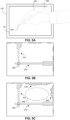
FIGS. 5A, 5B and 5C is a simplified schematic drawing of example simultaneous stylus and palm input to a device and schematic representations of corresponding example outputs when the device is grounded and ungrounded respectively in accordance with some example embodiments of the disclosure; -
FIGS. 6A and 6B is a simplified schematic drawing showing example simultaneous stylus and finger touch input to a device and schematic representations of corresponding example outputs from stylus detection when the device is ungrounded in accordance with some example embodiments of the disclosure; -
FIGS. 7A and 7B is a simplified schematic drawing showing an example simultaneous stylus and single touch input to a device and schematic representations of corresponding example outputs from stylus detection when the device is ungrounded in accordance with some example embodiments of the disclosure; -
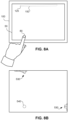
FIGS. 8A and 8B is a simplified schematic drawing showing example single-touch input to a device and schematic representations of corresponding example outputs from stylus detection when the device is ungrounded in accordance with some example embodiments of the disclosure; -
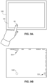
FIGS. 9A and 9B is a simplified schematic drawing showing example single-touch input to a device and schematic representations of corresponding example outputs from noise detection when the device is ungrounded in accordance with some example embodiments of the disclosure; -
FIG. 10 a simplified block diagram of an exemplary computing device including a touch and pen enabled track pad in accordance with some embodiments of the present disclosure; -
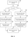
FIG. 11 is a simplified flow chart of an example method for selectively using output from stylus sampling window for palm rejection in accordance with some example embodiments of the disclosure; -
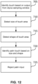
FIG. 12 is a simplified flow chart of an example palm rejection method based on output from stylus sampling window in accordance with some example embodiments of the disclosure; -
FIG. 13 is a simplified flow chart of an example method for touch and stylus detection in accordance with some example embodiments of the disclosure; and -
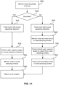
FIG. 14 is a simplified flow chart of an example method for touch detection in accordance with some example embodiments of the disclosure. - According to some example implementations, a digitizer system detects touch input on a touch sensitive surface based on output in a frequency range of the stylus. While the computing device is ungrounded, the stylus signal may find a path to ground via the user and the stylus signal transmitted through the user may appear at touch locations on the screen. According to some example implementations, these touch locations may be identified by the digitizer system and differentiated from a stylus signal detected at a location near a writing tip of the stylus. The touch locations may be detected over a sampling window dedicated for stylus detection, e.g. together with stylus detection. The differentiation may be based on gain of the output as well as shape of a spread of the output over the sensing surface.
- According to some example implementations, touch detection in a frequency range of the stylus is implemented for palm rejection. Palm input is typically difficult to detect based on mutual capacitive detection while the computing device is ungrounded. Due to a known retransmission effect, the relatively large touch area of the palm (large blob) may appear as a plurality of smaller touched areas (smaller blobs) that may be falsely identified as finger touch input. Palm detection based on the stylus signal injected through the user does not suffer from the retransmission effect and therefore the blob associated with palm input corresponds to the shape and size of the palm contact and may be clearly recognized as palm input.
- According to some example implementations, touch detection in a frequency range of the stylus is implemented for touch tracking of single touch while the computing device is ungrounded. Tracking touch based on detecting the injected stylus signal may be faster, less processing heavy, and performed with less power expenditure than touch tracking based on mutual capacitive detection. In some example embodiments, the digitizer system may temporarily suspend mutual capacitive detection or may temporarily reduce the refresh rate of mutual capacitive detection while the computing device is determined to be ungrounded and the conditions are suitable for touch detection based detection in a frequency range of the stylus. The digitizer system may in this case track the single touch input simultaneously with stylus detection, e.g. over the same sampling window. Since scanning is not typically needed for stylus signal detection, detection is quicker and the refresh rate may optionally be increased. Optionally, touch detection in a frequency range of the stylus is synchronized with transmission of the stylus signal.
- In some example implementations, touch input may be detected on an ungrounded touch sensitive surface based on output in a frequency range of noise in the surrounding environment. For example, noise from florescent lighting or from a two-prong power supply (ungrounded power supply) may be injected through the user and appear at touch locations while the user is interacting with the touch sensitive surface. These touch locations may be tracked while detecting output in a broad frequency band or at frequency bands specified for noise detection. Optionally, touch detection based on noise frequency may be detected in a sampling window at which the expected noise is typically detected. Touch locations may be differentiated from general noise based on gain and shape of a spread of the output over the sensing surface. Optionally, touch detection based on output in a noise frequency range may be performed without stylus transmission.
- For purposes of better understanding some embodiments of the present invention, as illustrated in
FIGS. 5A-14 of the drawings, reference is first made to the construction and operation of a computing device as illustrated inFIGS. 1-4B . - Reference is now made to
FIG. 1 showing a simplified block diagram of an exemplary touch and pen enabled computing device and to a simplified timeline of example sampling windows for sampling a grid based capacitive sensor.Computing device 100 includes adisplay 45 integrated with adigitizer sensor 50.Sensor 50 may be operated to detect both input bystylus 150 and to detect a finger effect due to one ormore fingertips 80 or other conductive objects interacting withsensor 50. Palm input fromhand 180 positioned over or resting onsensor 50 may also be detected.Digitizer sensor 50 typically includes a matrix formed with parallelconductive material 55 arranged in rows and columns with a capacitive connection injunction areas 59 formed between rows and columns.Digitizer sensor 50 may be operated bydigitizer circuit 25 and may be in communication withhost 22. Optionally,sensor 50 may not be integrated withdisplay 45 and may be instead integrated with an alternate sensing surface, e.g., a trackpad. -
Digitizer circuit 25 applies mutual capacitive detection or a self-capacitive detection for sensing a touch signal from touch (or hover) offingertip 80. Typically, mutual capacitive detection provides for detecting coordinates ofmultiple fingertips 80 touchingsensor 50 at the same time (multi-touch). Bringing a groundedfinger 80 close to the surface ofdigitizer sensor 50 changes the local electrostatic field and reduces the mutual capacitance atjunctions 59 in the touched area. A change in mutual capacitance may be detected bycircuit 25 when applying a drive signal along one axis (the drive lines) of the matrix while sampling output on the other axis (the receive lines) to detect a coupled signal. Mutual capacitive detection may be performed over one or more sampling windows 210 (FIG. 2 ) for each refresh cycle, Tcycle, ofdigitizer circuit 25. Typically, a plurality ofsampling windows 210 is defined to provide for scanning the entire area ofsensor 50 one drive at a time or a plurality of drive lines at a time based on mutual capacitive detection. - Finger touch generally has the effect of reducing amplitude of the measured signal. Output from
digitizer sensor 50 may be in the form of a heatmap that maps detected amplitudes of the coupled signals at eachjunction 59. In a heatmap, finger touch produces a negative blob at the touch location. When part of hand 180 (palm) hovers or rests ondigitizer sensor 50, a negative blob may also be recorded due to palm input. -
Digitizer circuit 25 may also detect input from astylus 150 emitting asignal 125 from itstip 120, e.g. writing tip.Stylus 150 may also emit a signal from aring 127 around itstip 120 and from aneraser end 128 ofstylus 150.Digitizer circuit 25 may also detect input fromring 127 anderaser end 128. During stylus detection,digitizer circuit 25 may simultaneously sampleconductive material 55 forming both the rows and columns to detectsignals 125 picked up byconductive material 55 near writing tip 120 (ring 127 or eraser end 128).Digitizer circuit 25 may detect stylus input over a dedicated stylus sampling window 220 (FIG. 2 ) in which both column and row conductive material 55 (drive and receive lines) are sampled. -
Signal 125 may be a pulsed signal transmitted at a defined repeat rate, e.g. every 5-20 msec. The pulsed signal may include a position signal (or beacon) and optionally a train of data defining a plurality of parameters. Optionally,stylus 150 is pressure sensitive and the data includes information indicating that the stylus is in one of a hover or touch operational mode. In some example embodiments, the data is based on a pressure sensor associated with writing tip 125 (or eraser end 128). Optionally, a separate sampling window may be defined to detect the train of data. Synchronization may be established between transmission ofsignal 125 andstylus sampling window 220. Optionally,digitizer circuit 25 synchronizes with transmissions ofsignal 125 andstylus sampling window 220 is adjusted based on timings ofsignal 125. Optionally, whiledigitizer circuit 25 is searching for stylus signal 125 more than onestylus sampling window 220 is defined per refresh cycle, Tcycle, ofdigitizer circuit 25. -
Digitizer circuit 25 may sample output in a frequency band of the drive signal over mutual capacitivedetection sampling windows 210 and may sample output in a frequency band of an expected stylus signal overstylus detection windows 220. Optionally,digitizer circuit 25 may also operate additional sampling windows such asnoise sampling windows 230. Optionally, a frequency band for sampling overnoise sampling window 230 may be defined over a wider frequency band that may include both frequency band of the drive signal and frequency band of an expected stylus signal. - Output from
digitizer circuit 25 is reported to host 22. Typically, the output provided bydigitizer circuit 25 includes coordinates of one ormore fingertips 80 and coordinates of writingtip 120 when present.Digitizer circuit 25 may be configured to differentiate between input fromfingertip 80 and input fromhand 180 and may selectively refrain from reporting coordinates ofhand 180 based on a defined palm rejection method. Additional information related to parameters ofstylus 150, noise being picked up bysensor 50 and a grounding state ofdevice 100 may also be detected withdigitizer circuit 25 based on input fromdigitizer sensor 50. The additional information detected may be reported tohost 22.Digitizer circuit 25 may distinguish between input received by hover or touch and may report one of a hover or touch state to host 22 together with the detected coordinates of the input. Optionally, some or all of the functionalities ofdigitizer circuit 25 may be integrated intohost 22. -
FIG. 3 shows a schematic representation of the relative effect on a grid based capacitive sensor with one finger touching the digitizer sensor. Only a portion ofdigitizer sensor 50 is shown for simplicity. A presence of afingertip 80 atlocation 320 reduces mutual capacitance atjunctions 59 inlocation 320. Due to the reduced mutual capacitance, when adrive signal 305 is imposed ondrive lines 56, amplitudes detected on the touched receivelines 57 are lower than amplitude detected on other receivelines 57. Reduced amplitudes due to the reduced mutual capacitances are represented byarrows 310. - At the same time, potential may be induced on the finger from
drive signal 305. This typically occurs while the device is not grounded due to the difference in potential between the user that is grounded and the device. The potential induced on the finger from drive signal 305may be injected on receivelines 57 which increases amplitudes of the outputs as represented byarrows 315. The output detected from the touched receive lines is therefore a summation ofamplitude 310 andamplitude 315. Typically, output detected from a single finger touch produces a negative blob having amplitude that varies based on the magnitude of the induced potential. This amplitude sometimes called the finger effect may be used as an indication of a grounding state of the computing device. Low amplitude, e.g. below a defined threshold, due to large induced potential may indicate that the device is ungrounded while high amplitude, e.g. above the defined threshold, due to a small induced potential may indicate that the device is grounded. A grounding state of the device may be monitored by digitizer circuit 25 (FIG. 1 ) and optionally reported to host 22. -
FIG. 4A and 4B show example heatmaps and corresponding two dimensional blobs of example palm touch signal for a device that is grounded and ungrounded respectively.Heatmaps heat map 410 andblob 420 defined byheat map 410 may appears as a single area that may be clearly distinguished from single finger touch input. However, when a computing device has high impedance to ground, e.g. is ungrounded, a same palm input may produce a heatmap,e.g. heatmap 430 that provides a peak that is not well defined. Distortions inheat map 430 are due to coupling of potentials picked up by the palm that reverse the effect of the touch signal. These distortions may lead to a single palm touch area being depicted as a plurality ofseparate blobs FIG. 1 ) may mistakenly identify the palm input as three close finger touches based onheatmap 430. - Reference is now made to
FIGS. 5A, 5B and 5C showing a simplified schematic drawing of example simultaneous stylus and palm input to a device and schematic representations of corresponding example outputs when the device is grounded and ungrounded respectively in accordance with some example embodiments of the disclosure. While a user is providing input withstylus 150, ahand 180 holdingstylus 150 or optionally the opposite hand of the user may be resting onsensor 50. As long asdevice 100 is well grounded, output detected over stylus sampling window 220 (FIG. 2 ) is not affected by contact ofhand 180 onsensor 50 as shown inFIG. 5B .Device 100 may be well grounded while connected to a power supply with a three-prong connector or based on a user physically contacting a chassis of the device. Whiledevice 100 is grounded, output detected may typically show a sharp peak inamplitude 510 in both the row and columnconductive material 55 that indicate stylus input atlocation 520.Peaks 510 may be less sharp whenstylus 150 is hovering as opposed to touchingdevice 100. -
FIG. 5B shows example output detected overstylus sampling window 220 whiledevice 100 is ungrounded.Device 100 may be ungrounded while connected to power supply with a two-prong connector or while the device is resting on non-conductive surface. Whiledevice 100 is not grounded, physical contact betweenhand 180 andstylus 150 may induce a potential onhand 180 in a frequency band of signal 125 (from writingtip 120,ring 127 or eraser 128). Contact ofhand 180 in a vicinity ofconductive strips 55 picking upsignal 125 may also induce a potential onhand 180 in the frequency band ofsignal 125. Due to the induced potential,output 530 on each of the row and columnconductive materials 55 in anarea 540 of hand touch that may be detected in thestylus sampling window 220. Amplitude ofoutput 530 due tohand 180 picking up potential fromsignal 125 is typically significantly lower in amplitude as compared tooutput 510 detected onsensor 50 directly fromstylus 150.Amplitude 510 is not expected to differ significantly between a grounded and ungrounded state of the device when using a non-conductive housing for the stylus due to the relatively high impedance between the user and the stylus. - According to some example embodiments,
digitizer circuit 25 is configured to detect both stylus input and hand input over astylus sampling window 220 and to distinguish between them. In some example embodiments, stylus input is identified as a peak spread over a defined number ofconductive strips 55 and having amplitude above a defined stylus amplitude threshold, while hand input is identified as a peak spread over a larger number ofconductive strips 55 and having amplitude in a defined range below the defined stylus amplitude threshold. - In some example embodiments, touch detection over the stylus sampling window, e.g. in the stylus frequency range is applied to track palm input and to perform palm rejection while
device 100 is in an ungrounded state, e.g. poorly grounded. Since output 530 (FIG. 5C ) is not detected while drive signals are transmitted onsensor 55 and the output does not suffer from distortions due to potentials picked up by the palm having a reverse the effect of the touch signal.Digitizer circuit 25 may classify size and shape ofarea 540 and determine thatarea 540 is palm input based on the classification. In some example embodiments, a heatmap, e.g. heatmap 430 (FIG. 4B ) detected over a mutual capacitive sampling window may be verified as input from a palm based on comparing location of touch inputs in the heatmap detected over the mutualcapacitive sampling periods 210 with location of area 540 (FIG. 5C ) detected over thestylus sampling period 220. - Reference is now made to
FIGS. 6A and 6B showing a simplified schematic drawing showing example simultaneous stylus and finger touch input to a device and schematic representations of corresponding example outputs from stylus detection when the device is ungrounded in accordance with some example embodiments of the disclosure. In some example embodiments, while onehand 180 is holdingstylus 150, signal 125 may induce a potential on a user that may be detected onsensor 50 when one ormore fingertips 80 from the opposite hand simultaneously touchessensor 50. This may occur whiledevice 100 is in an ungrounded state. In some example embodiments, adistinct peak 530 may be detected in the row and column direction for each finger touch over a stylus sampling window. However, coordinates of multiple touches may not always be resolvable based onoutput 530. For example touch of twofingers 80 may correspond to fourpotential touch locations 540 based onoutputs 530 two of which may be the touch locations and two others may be ghost locations. - In some example embodiments,
digitizer circuit 25 may define aninclusive area 550 including allpotential touch locations 540 and may use this information during mutual capacitive detection. Optionally,digitizer circuit 25 may reduce an area that is scanned during mutual capacitive detection (optionally only scan area 550) based onarea 550 detected over thestylus sampling window 220. Optionally, by reducing the number of drive lines that are scanned, the number of mutual capacitivedetection sampling windows 210 may be reduced. Optionally reducing refresh rate. - Reference is now made to
FIGS. 7A and 7B showing a simplified schematic drawing of an example simultaneous stylus and single touch input to a device and schematic representations of corresponding example outputs from stylus detection when the device is ungrounded in accordance with some example embodiments of the disclosure. According to some example embodiments, during an ungrounded state ofdevice 100,stylus input 520 along withsingle touch input 540 may be detected over astylus sampling window 220.Single touch input 540 may be detected based on potential induced onfinger 80 touchingsensor 50 while anopposite hand 180 is holdingstylus 150. In some example embodiments,digitizer circuit 25 detectssingle touch 540 input over a stylus sampling window and may report coordinates oftouch 540 based onoutput 530 detected overstylus sampling window 220. Optionally,digitizer circuit 25 may reduce the number or the frequency of mutual capacitivedetection sampling windows 210 while detecting asingle touch 540 isstylus sampling window 220. Optionally, whiledevice 100 is determined to be ungrounded,digitizer circuit 25 may also reduce the number ofsampling windows 210 or the refresh rate of mutual capacitive detection when notouch area 540 is detected overstylus sampling period 220. - Reference is now made to
FIGS. 8A and 8B showing a simplified schematic drawing of an example single-touch input on a device and schematic representations of corresponding example outputs from stylus detection when the device is ungrounded in accordance with some example embodiments of the disclosure. In some example embodiments, touch withfingertip 80 may be detected onsensor 50 over astylus detection period 220 even when the user is not holdingstylus 150. Forexample stylus 150 may be laying oversensor 50 or adjacent tosensor 50. Optionally, as long asstylus 150 is emittingsignal 125 in a vicinity of sensor 50 (by hovering or touching the touch screen), a potential fromsignal 125 may be induced onfingertip 80 touchingsensor 50 whiledevice 100 is in an ungrounded state. In some example embodiments,touch 540 may be detected based onoutput 530 detected overstylus sampling period 230. Amplitude of peaks inoutput 530 may be lower during a hover mode ofstylus 150, e.g. while the writing tip or eraser end is not touchingsensor 50. In some example embodiments, a threshold for detectingtouch 540 may be reduced during a hover operational mode. Optionally, the digitizer system may differentiate between a hover and touch mode ofstylus 150, e.g. based on a sensor instylus 150. The threshold for detectingtouch 540 may be reduced based on information received fromstylus 150. - Reference is now made to
FIGS. 9A and 9B showing a simplified schematic drawing showing example single-touch input to a device and schematic representations of corresponding example outputs from noise detection when the device is ungrounded in accordance with some example embodiments of the disclosure. In some example embodiments, touch may be detected over various sampling windows, e.g. other than thestylus sampling window 220 and other than the mutual capacitivedetection sampling window 210. In some examples, touch may also be detected over anoise sampling window 230 as long asdevice 100 is in an ungrounded state. In some example embodiments,device 100 may be exposed to noise, e.g. noise from florescent lighting or from a two-prong power supply (ungrounded power supply) and potential from this noise may be induced on fingertip 80 (or hand 180) touchingsensor 50 whiledevice 100 is ungrounded. The induced potential from the noise may provide a touch signal in the noise sampling period as long as the noise is in a frequency range sampled. Optionally,digitizer circuit 25 may detect and trackfinger touch 540 based onoutput 531 detected in the noise window. - Reference is now made to
FIG. 10 showing a simplified block diagram of an exemplary computing device including a touch and pen enabled trackpad in accordance with some embodiments of the present disclosure. According to some example embodiments, adevice 200 may include atrackpad 250 as a touch sensitive surface that is both touch and pen enabled. Optionally,display 201 ofdevice 200 may or may not be touch and pen enabled.Trackpad 250 may include a grid based capacitive sensor that may be sensitive to a grounding state ofdevice 200. According to some example implementations, the methods described herein to detect touch and perform palm rejection may be similarly applied to track touch and perform palm rejection ontrackpad 250. - Reference is now made to
FIG. 11 showing a simplified flow chart of an example method for selectively using output from stylus sampling window for palm rejection in accordance with some example embodiments of the disclosure. In some example embodiments, a grounding state of a touch and pen enabled device is monitored (block 605). Optionally, the device includes a grounding state machine that may detect a grounding state of the device based on relative effects of selected output detected with mutual capacitive detection. In some example embodiments, as long as the device is determined to be grounded (block 610), touch input may be detected over sampling windows dedicated to mutual capacitive detection (block 615). Palm rejection may be based on size and shape of touch area detected during mutual capacitive detection (block 620). Stylus input may be detected over a dedicated stylus sampling window (block 635). Output of the sensor over the stylus sampling window is sampled in a frequency of a signal transmitted by the stylus. Coordinates of finger touch, e.g. intended touch and stylus may be reported to the host computer (block 650). - In some example embodiments, while the device is determined to be ungrounded (block 610), touch may still be tracked with mutual capacitive detection (block 630) and but may also be tracked over a stylus sampling window together with tracking stylus input (block 635). Optionally, the refresh rate for mutual capacitive detection may be reduced while the device is determined to be ungrounded. In some example embodiments, palm rejection may be performed or verified based on touch detected in the stylus sampling window (block 640). Coordinates of finger touch, e.g. intended touch and stylus may be reported to the host computer (block 650)
- Reference is now made to
FIG. 12 showing a simplified flow chart of an example palm rejection method based on output from stylus sampling window in accordance with some example embodiments of the disclosure. In some example embodiments, touch input may be identified based on output from the stylus sampling window, e.g. output in a frequency range of the stylus signal. In some example embodiments, a touch signal is distinguished from a stylus signal based on amplitude of the output. Output due to touch may be expected to have a lower amplitude and be spread over more conductive lines of the grid based sensor as compared to output due to a stylus tip (eraser end or ring around tip) interacting with the digitizer sensor. In some example embodiments, size of the touch area (block 710) and a shape characteristic of the touch area (block 715) may be detected and palm may be identified based on classification of the size and shape detected (block 720). Optionally, palm input may be rejected, e.g. its location may not be reported to the host computer (block 725). - Reference is now made to
FIG. 13 showing a simplified flow chart of an example method for touch and stylus detection in accordance with some example embodiments of the disclosure. In some example embodiments, a grounding state of a touch and pen enabled device is monitored (block 805). In some example embodiments, as long as the device is determined to be grounded (block 810), touch input may be detected over sampling windows dedicated to mutual capacitive detection and at a standard refresh rate(block 815). Stylus input may be tracked substantially simultaneously over dedicated stylus sampling windows (block 820). Touch and stylus location may be reported to the host computer (block 850). - In some example embodiments, while the device is determined to be ungrounded (810) and single touch input is identified (block 825), a refresh rate for mutual capacitive detection may be reduced (block 830) and touch tracking may be performed or supplemented based on output from stylus sampling window as long as a stylus signal is being received by the digitizer sensor. Both touch and stylus may be detected over the stylus sampling window (block 835). Touch and stylus location may be reported to the host computer (block 850).
- Reference is now made to
FIG. 14 showing a simplified flow chart of an example method for touch detection in accordance with some example embodiments of the disclosure. In some example embodiments, a grounding state of a touch and pen enabled device is monitored (block 905). In some example embodiments, as long as the device is determined to be grounded (block 910), touch input may be detected over sampling windows dedicated to mutual capacitive detection (block 915). Palm rejection may be based on size and shape of touch area detected during mutual capacitive detection (block 920) and noise may be monitored over dedicated noise sampling windows (block 925). Finger touch locations, e.g. intended touch may be reported to the host computer (block 930). - In some example embodiments, while the device is determined to be ungrounded (block 910), touch input may still be detected over mutual capacitive sampling windows and may also be detected together with noise over noise sampling windows (block 940). Palm rejection may be performed or verified based on touch input detected in the noise sampling window (block 945). Optionally, touch may be tracked together with noise monitoring based on output detected over the noise sampling window (block 950).
- According to an aspect of some example embodiments, there is provided a method comprising: sampling output in a frequency range of a signal emitted from a stylus over a stylus sampling window, wherein the sampling is performed simultaneously from both columns and rows of a grid based capacitive sensor; detecting stylus input based on detecting a gain above a stylus threshold in at least one column and one row of the sensor; reporting coordinates of the stylus based on stylus input being detected; detecting touch input from a finger or hand based on detecting a gain between a touch threshold and a stylus threshold, wherein the touch threshold is below the stylus threshold over at least two consecutive columns and two consecutive rows of the sensor; and reporting coordinates of the touch input based on detecting the touch input.
- Optionally, the method includes determining that a device including the grid based capacitive sensor is either grounded or ungrounded; and detecting the touch input from the finger or hand based on the output in the stylus frequency range only when the device is ungrounded.
- Optionally, the method includes performing mutual capacitive detection; determining gains of selected touch areas detected over the mutual capacitive detection; determining that the device either grounded or ungrounded based on the gains.
- Optionally, the method includes detecting a heatmap on the grid based capacitive sensor based on mutual capacitive detection; identifying a plurality of blobs on the heatmap; comparing an area of the touch input detected over the stylus sampling window with the plurality of blobs identified in the heatmap; and reporting the coordinates of the touch input based on the comparing.
- Optionally, the method includes performing palm rejection based on the comparing and refraining from reporting coordinates of the palm input.
- Optionally, the method includes determining size of the touch input; and identifying the touch input as palm input based on the size.
- Optionally, the method includes determining a shape characteristic of a spread of the touch input over the sensor; and identifying the touch input as palm input based on the size.
- Optionally, the method includes identifying a single area of the touch input over the stylus sampling window; and reducing a refresh rate for mutual capacitive detection of the sensor based on identifying the single area of the touch input.
- Optionally, the method includes identifying a single area of the touch input over the stylus sampling window; and temporarily suspending mutual capacitive detection of the sensor based on identifying the single area of the touch input.
- Optionally, the method includes identifying a plurality of touch inputs over a defined area over the stylus sampling window; and performing mutual capacitive detection of the sensor only over the defined area.
- According to an aspect of some example embodiments, there is provided a method including determining that a device that includes a grid based capacitive sensor is either grounded or ungrounded; and sampling output of the grid based capacitive sensor over a plurality of sampling windows; performing mutual capacitive detection over a first sampling window from the plurality; sampling output from both columns and rows of the grid based sensor over a second sampling window from the plurality, wherein the output is sampled without driving the column or rows with a driving signal emitted by a controller configured to operate the grid based capacitive sensor; identifying a heatmap based on the mutual capacitive detection over the first sampling window; identifying areas of touch input from the output sampled over the second sampling window based on determining that the device is ungrounded; comparing the heatmap to the areas of touch input identified based on determining that the device is ungrounded; and reporting coordinates of touch based on the comparing.
- Optionally, the second sampling window is a sampling window configured for tracking a stylus, wherein the stylus is configured to transmit a signal.
- Optionally, the second sampling window is a sampling window configured for sampling a noise environment of the grid based capacitive sensor.
- Optionally, the output sampled over the second sampling window is in a frequency range of noise from a power supply that is not grounded or in a frequency range of noise based on fluorescent lights.
- Optionally, the method includes performing palm rejection based on identifying the areas of touch input from the output sampled over the second sampling window.
- Optionally, the method includes determining a size of the areas of the touch input from the output sampled over the second sampling window; determining a shape characteristic of a spread over the sensor of the areas of the touch input from the output sampled; and identifying at least one of the areas as palm input based on the shape.
- Optionally, the method includes identifying a plurality of blobs on the heatmap; comparing the areas of the touch input detected over the second sampling window with the plurality of blobs identified in the heatmap; and reporting the coordinates of the touch input based on the comparing.
- Optionally, the includes identifying at least a portion of the plurality of blobs as palm input based on the comparing and refraining from reporting coordinates of the palm input.
- Optionally, the method includes identifying a single area of the touch input over the second sampling window; and reducing a number of sampling windows in which mutual capacitive detection is performed over subsequent refresh periods based on identifying the single area of the touch input.
- Optionally, the method includes identifying a single area of the touch input over the second sampling window; and temporarily suspending mutual capacitive detection of the sensor over subsequent refresh periods of the sensor based on identifying the single area of the touch input.
- Certain features of the examples described herein, which are, for clarity, described in the context of separate embodiments, may also be provided in combination in a single embodiment. Conversely, various features of the examples described herein, which are, for brevity, described in the context of a single embodiment, may also be provided separately or in any suitable sub-combination or as suitable in any other described embodiment of the disclosure. Certain features described in the context of various embodiments are not to be considered essential features of those embodiments, unless the embodiment is inoperative without those elements.
Claims (7)
- A method comprising:determining that a device that includes a grid based capacitive sensor (50) is either grounded or ungrounded; andsampling the output of the grid based capacitive sensor (50) over a plurality of sampling windows (210);performing mutual capacitive detection over a first sampling window from the plurality of sampling windows (210);sampling the output from both columns and rows of the grid based capacitive sensor (50) over a second sampling window from the plurality of sampling windows (210), wherein the output is sampled without driving the column or rows with a driving signal emitted by a controller configured to operate the grid based capacitive sensor (50);identifying a heatmap (410; 430) based on the mutual capacitive detection over the first sampling window;identifying areas of touch input from the output sampled over the second sampling window based on determining that the device (100) is ungrounded;comparing the heatmap to the areas of touch input (540) identified based on determining that the device is ungrounded; andreporting the coordinates of the touch based on the comparing.
- The method according to claim 1, wherein the second sampling window is a sampling window configured for tracking a stylus (150), wherein the stylus (150) is configured to transmit a signal.
- The method according to claim 1, wherein the second sampling window is a sampling window configured for sampling a noise environment of the grid based capacitive sensor (50), and wherein the output sampled over the second sampling window is in a frequency range of noise from a power supply that is not grounded or in a frequency range of noise based on fluorescent lights.
- The method according to claim 1, comprising:determining a size of the areas of the touch input (540) from the output sampled over the second sampling window;determining a shape characteristic of a spread over the sensor (50) of the areas of the touch input (540) from the output sampled; andidentifying at least one of the areas as palm input based on the shape; andperforming palm rejection based on identifying the areas of touch input (540) from the output sampled over the second sampling window.
- The method according to claim 1, comprising:identifying a plurality of blobs (442, 444, 446) on the heatmap (410; 430);comparing the areas of the touch input (540) detected over the second sampling window with the plurality of blobs (442, 444, 446) identified in the heatmap (410 ;430);reporting the coordinates of the touch input (540) based on the comparing; andidentifying at least a portion of the plurality of blobs (442, 444, 446) as palm input based on the comparing and refraining from reporting coordinates of the palm input.
- The method according to claim 1, comprising:identifying a single area of the touch input (540) over the second sampling window; andreducing a number of sampling windows (210) in which mutual capacitive detection is performed over subsequent refresh periods based on identifying the single area of the touch input (540).
- The method according to claim 1, comprising:identifying a single area of the touch input (540) over the second sampling window; andtemporarily suspending mutual capacitive detection of the sensor (50) over subsequent refresh periods of the sensor (50) based on identifying the single area of the touch input (540).
Applications Claiming Priority (3)
| Application Number | Priority Date | Filing Date | Title |
|---|---|---|---|
| US15/917,865 US10678348B2 (en) | 2018-03-12 | 2018-03-12 | Touch detection on an ungrounded pen enabled device |
| PCT/US2019/020463 WO2019177795A1 (en) | 2018-03-12 | 2019-03-03 | Touch detection on an ungrounded pen enabled device |
| EP19711767.4A EP3750039B1 (en) | 2018-03-12 | 2019-03-03 | Touch detection on an ungrounded pen enabled device |
Related Parent Applications (2)
| Application Number | Title | Priority Date | Filing Date |
|---|---|---|---|
| EP19711767.4A Division-Into EP3750039B1 (en) | 2018-03-12 | 2019-03-03 | Touch detection on an ungrounded pen enabled device |
| EP19711767.4A Division EP3750039B1 (en) | 2018-03-12 | 2019-03-03 | Touch detection on an ungrounded pen enabled device |
Publications (3)
| Publication Number | Publication Date |
|---|---|
| EP4231123A2 true EP4231123A2 (en) | 2023-08-23 |
| EP4231123A3 EP4231123A3 (en) | 2023-10-11 |
| EP4231123B1 EP4231123B1 (en) | 2025-02-26 |
Family
ID=65812417
Family Applications (2)
| Application Number | Title | Priority Date | Filing Date |
|---|---|---|---|
| EP23185259.1A Active EP4231123B1 (en) | 2018-03-12 | 2019-03-03 | Touch detection on an ungrounded pen enabled device |
| EP19711767.4A Active EP3750039B1 (en) | 2018-03-12 | 2019-03-03 | Touch detection on an ungrounded pen enabled device |
Family Applications After (1)
| Application Number | Title | Priority Date | Filing Date |
|---|---|---|---|
| EP19711767.4A Active EP3750039B1 (en) | 2018-03-12 | 2019-03-03 | Touch detection on an ungrounded pen enabled device |
Country Status (4)
| Country | Link |
|---|---|
| US (1) | US10678348B2 (en) |
| EP (2) | EP4231123B1 (en) |
| CN (1) | CN111902798B (en) |
| WO (1) | WO2019177795A1 (en) |
Families Citing this family (13)
| Publication number | Priority date | Publication date | Assignee | Title |
|---|---|---|---|---|
| US10616349B2 (en) | 2018-05-01 | 2020-04-07 | Microsoft Technology Licensing, Llc | Hybrid sensor centric recommendation engine |
| CN113853566B (en) | 2019-07-26 | 2024-05-28 | 谷歌有限责任公司 | Context-sensitive control based on radar gesture recognition |
| EP4127882B1 (en) * | 2020-03-25 | 2026-07-08 | Microsoft Technology Licensing, LLC | Uplink channel compensation for touchscreen devices |
| CN113178900B (en) | 2021-03-15 | 2023-02-17 | 荣耀终端有限公司 | Wireless charging system, chip and wireless charging circuit |
| US11592925B1 (en) * | 2021-11-09 | 2023-02-28 | Synaptics Incorporated | Low latency input object detection under low ground mass condition |
| US20230152923A1 (en) * | 2021-11-17 | 2023-05-18 | Cirque Corporation | Palm Detection Using Multiple Types of Capacitance Measurements |
| US12182363B2 (en) * | 2022-06-22 | 2024-12-31 | Microsoft Technology Licensing, Llc | Touchscreen sensor calibration using adaptive noise classification |
| CN115454275B (en) * | 2022-09-19 | 2023-07-28 | 深圳市坤巨实业有限公司 | Quality detection method and device for capacitive touch screen and computer equipment |
| WO2025071624A1 (en) | 2023-09-29 | 2025-04-03 | Google Llc | Screen protector presence detection |
| US20250147618A1 (en) * | 2023-11-06 | 2025-05-08 | Novatek Microelectronics Corp. | Touch device and operation method thereof |
| CN120523338A (en) * | 2024-02-21 | 2025-08-22 | 北京小米移动软件有限公司 | Anti-accidental touch method, device, electronic device, storage medium and computer program product |
| US20260050334A1 (en) * | 2024-08-16 | 2026-02-19 | Pixart Imaging Inc. | Touchpad device and method for generating touchpad information |
| WO2026142703A1 (en) * | 2024-12-26 | 2026-07-02 | Google Llc | Touch-based hover-gesture suppression |
Family Cites Families (153)
| Publication number | Priority date | Publication date | Assignee | Title |
|---|---|---|---|---|
| US4686332A (en) | 1986-06-26 | 1987-08-11 | International Business Machines Corporation | Combined finger touch and stylus detection system for use on the viewing surface of a visual display device |
| US4398720A (en) | 1981-01-05 | 1983-08-16 | California R & D Center | Robot computer chess game |
| US4591710A (en) | 1983-07-11 | 1986-05-27 | Electro Mechanical Systems, Inc. | Ambient light and electromagnetic noise reduction circuit |
| US4672154A (en) | 1985-04-03 | 1987-06-09 | Kurta Corporation | Low power, high resolution digitizing system with cordless pen/mouse |
| US4791592A (en) | 1986-04-30 | 1988-12-13 | Hewlett-Packard Company | Method and apparatus for reducing jitter in a digitizer or other transducer |
| US4707845A (en) | 1986-08-26 | 1987-11-17 | Tektronix, Inc. | Touch panel with automatic nulling |
| US4977397A (en) | 1989-10-13 | 1990-12-11 | Sysgration Ltd. | Touch-control computer house |
| IL96620A0 (en) | 1990-12-23 | 1991-09-16 | Marc Zuta | Electrical input device and method |
| US5117071A (en) | 1990-10-31 | 1992-05-26 | International Business Machines Corporation | Stylus sensing system |
| US5129654A (en) | 1991-01-03 | 1992-07-14 | Brehn Corporation | Electronic game apparatus |
| JPH05173698A (en) | 1991-12-25 | 1993-07-13 | Seiko Instr Inc | Coordinate reading device |
| DE69324067T2 (en) | 1992-06-08 | 1999-07-15 | Synaptics Inc | Object position detector |
| US5543588A (en) | 1992-06-08 | 1996-08-06 | Synaptics, Incorporated | Touch pad driven handheld computing device |
| US6239389B1 (en) | 1992-06-08 | 2001-05-29 | Synaptics, Inc. | Object position detection system and method |
| US5973676A (en) | 1993-06-30 | 1999-10-26 | Kabushiki Kaisha Toshiba | Input apparatus suitable for portable electronic device |
| US5528002A (en) | 1993-07-15 | 1996-06-18 | Pentel Kabushiki Kaisha | Noiseproof digitizing apparatus with low power cordless pen |
| JPH07311647A (en) | 1994-05-16 | 1995-11-28 | Wacom Co Ltd | Position detection device and noise removal method thereof |
| JP3186946B2 (en) | 1994-05-31 | 2001-07-11 | シャープ株式会社 | Coordinate detection device |
| JPH08106358A (en) | 1994-08-10 | 1996-04-23 | Fujitsu Ltd | Liquid crystal display device with tablet function, active matrix liquid crystal display device, and driving method of liquid crystal display device with tablet function |
| US5574262A (en) | 1994-10-04 | 1996-11-12 | At&T Global Information Solutions Company | Noise cancellation for non-ideal electrostatic shielding |
| JP3015275B2 (en) | 1995-04-10 | 2000-03-06 | 株式会社ワコム | Position detecting device and position indicator used therein |
| JP3678801B2 (en) | 1995-08-02 | 2005-08-03 | シャープ株式会社 | Integrated display tablet device |
| US5859392A (en) | 1996-02-09 | 1999-01-12 | Lsi Logic Corporation | Method and apparatus for reducing noise in an electrostatic digitizing tablet |
| JP3251489B2 (en) | 1996-02-16 | 2002-01-28 | シャープ株式会社 | Coordinate input device |
| JP3436637B2 (en) | 1996-06-04 | 2003-08-11 | アルプス電気株式会社 | Coordinate input device |
| JPH1031545A (en) | 1996-07-17 | 1998-02-03 | Nippon Syst Kaihatsu Kk | Input device |
| US5889511A (en) | 1997-01-17 | 1999-03-30 | Tritech Microelectronics International, Ltd. | Method and system for noise reduction for digitizing devices |
| US6229529B1 (en) | 1997-07-11 | 2001-05-08 | Ricoh Company, Ltd. | Write point detecting circuit to detect multiple write points |
| US6081259A (en) | 1997-11-25 | 2000-06-27 | Lsi Logic Corporation | Method and apparatus for reducing noise in an electrostatic digitizer |
| US7663607B2 (en) | 2004-05-06 | 2010-02-16 | Apple Inc. | Multipoint touchscreen |
| KR100595926B1 (en) | 1998-01-26 | 2006-07-05 | 웨인 웨스터만 | Method and apparatus for integrating manual input |
| US6459424B1 (en) | 1999-08-10 | 2002-10-01 | Hewlett-Packard Company | Touch-sensitive input screen having regional sensitivity and resolution properties |
| US6417846B1 (en) | 2000-02-02 | 2002-07-09 | Lee Si-Ken | Multifunction input device |
| US6690156B1 (en) | 2000-07-28 | 2004-02-10 | N-Trig Ltd. | Physical object location apparatus and method and a graphic display device using the same |
| JP2002207563A (en) | 2001-01-05 | 2002-07-26 | Wacom Co Ltd | Position detection device |
| US6624835B2 (en) | 2001-01-09 | 2003-09-23 | National Semiconductor Corporation | System and method for noise reduction in touch screen system |
| WO2003005293A2 (en) | 2001-06-29 | 2003-01-16 | Hans Rudolf Sterling | Apparatus for sensing the position of a pointing object |
| EP2261777A1 (en) | 2001-08-22 | 2010-12-15 | Sharp Kabushiki Kaisha | Display device with a touch sensor for generating position data and method therefor |
| US7158121B2 (en) | 2001-10-19 | 2007-01-02 | American Standard International Inc. | Enhanced touch-screen display system |
| TW528981B (en) | 2001-10-25 | 2003-04-21 | Compal Electronics Inc | Portable computer and related method for preventing input interruption by write-tracking input region |
| JP2004070771A (en) | 2002-08-08 | 2004-03-04 | Fujitsu Component Ltd | Input device |
| WO2004021328A2 (en) | 2002-08-29 | 2004-03-11 | N-Trig Ltd. | Transparent digitiser |
| KR100456155B1 (en) | 2002-11-13 | 2004-11-09 | 엘지.필립스 엘시디 주식회사 | Touch panel aparatus and method for controling the same |
| KR100449745B1 (en) | 2002-11-21 | 2004-09-22 | 삼성전자주식회사 | Apparatus and Method for avoiding noise of touch screen |
| DE10254614B4 (en) | 2002-11-22 | 2006-04-20 | Infineon Technologies Ag | Method for detecting a relative movement of a finger relative to a sensor surface |
| US7372455B2 (en) | 2003-02-10 | 2008-05-13 | N-Trig Ltd. | Touch detection for a digitizer |
| GB0319945D0 (en) | 2003-08-26 | 2003-09-24 | Synaptics Uk Ltd | Inductive sensing system |
| US7995036B2 (en) | 2004-02-27 | 2011-08-09 | N-Trig Ltd. | Noise reduction in digitizer system |
| EP1787281A2 (en) | 2004-07-15 | 2007-05-23 | N-Trig Ltd. | Automatic switching for a dual mode digitizer |
| JP2006039686A (en) | 2004-07-22 | 2006-02-09 | Pioneer Electronic Corp | Touch panel device, touch region detecting method, and touch region detecting program |
| GB0417075D0 (en) | 2004-07-30 | 2004-09-01 | Hewlett Packard Development Co | Calibrating digital pens |
| US7847789B2 (en) | 2004-11-23 | 2010-12-07 | Microsoft Corporation | Reducing accidental touch-sensitive device activation |
| CN101133382B (en) | 2004-12-01 | 2016-03-30 | 微软技术许可有限责任公司 | Location detection system and the apparatus and method for using and control this location detection system |
| US20060139339A1 (en) | 2004-12-29 | 2006-06-29 | Pechman Robert J | Touch location determination using vibration wave packet dispersion |
| US7868874B2 (en) | 2005-11-15 | 2011-01-11 | Synaptics Incorporated | Methods and systems for detecting a position-based attribute of an object using digital codes |
| US8018440B2 (en) | 2005-12-30 | 2011-09-13 | Microsoft Corporation | Unintentional touch rejection |
| KR101227678B1 (en) | 2006-02-10 | 2013-01-30 | 삼성전자주식회사 | Human body communication system and method |
| US7244901B1 (en) | 2006-04-11 | 2007-07-17 | Danotech Co., Ltd. | Capacitive touch panel |
| US8059102B2 (en) | 2006-06-13 | 2011-11-15 | N-Trig Ltd. | Fingertip touch recognition for a digitizer |
| US9069417B2 (en) | 2006-07-12 | 2015-06-30 | N-Trig Ltd. | Hover and touch detection for digitizer |
| US8686964B2 (en) | 2006-07-13 | 2014-04-01 | N-Trig Ltd. | User specific recognition of intended user interaction with a digitizer |
| US7855718B2 (en) | 2007-01-03 | 2010-12-21 | Apple Inc. | Multi-touch input discrimination |
| US9746981B2 (en) | 2007-03-29 | 2017-08-29 | Microsoft Technology Licensing, Llc | System and method for multiple object detection on a digitizer system |
| US9654104B2 (en) | 2007-07-17 | 2017-05-16 | Apple Inc. | Resistive force sensor with capacitive discrimination |
| EP2212764B1 (en) | 2007-10-11 | 2017-06-14 | Microsoft Technology Licensing, LLC | Method for palm touch identification in multi-touch digitizing systems |
| US9075483B2 (en) | 2007-12-21 | 2015-07-07 | Apple Inc. | Negative pixel compensation |
| WO2009108334A2 (en) | 2008-02-28 | 2009-09-03 | New York University | Method and apparatus for providing input to a processor, and a sensor pad |
| US8289289B2 (en) | 2008-04-03 | 2012-10-16 | N-trig, Ltd. | Multi-touch and single touch detection |
| US8810542B2 (en) | 2008-09-10 | 2014-08-19 | Apple Inc. | Correction of parasitic capacitance effect in touch sensor panels |
| US8402391B1 (en) | 2008-09-25 | 2013-03-19 | Apple, Inc. | Collaboration system |
| US8482545B2 (en) | 2008-10-02 | 2013-07-09 | Wacom Co., Ltd. | Combination touch and transducer input system and method |
| GB2466566B (en) | 2008-12-22 | 2010-12-22 | N trig ltd | Digitizer, stylus and method of synchronization therewith |
| CN102265244B (en) | 2008-12-24 | 2015-08-26 | 株式会社半导体能源研究所 | Touch panel and driving method thereof |
| US8305358B2 (en) | 2009-02-10 | 2012-11-06 | Sony Ericsson Mobile Communications Ab | Sensor, display including a sensor, and method for using a sensor |
| US8278571B2 (en) | 2009-04-03 | 2012-10-02 | Pixart Imaging Inc. | Capacitive touchscreen or touchpad for finger and active stylus |
| TWI398807B (en) | 2009-04-07 | 2013-06-11 | Ite Tech Inc | Posistion apparatus for touch device and posistion method thereof |
| TWI466004B (en) * | 2009-04-17 | 2014-12-21 | Egalax Empia Technology Inc | Method and device for resistive multi-point touch |
| US8169418B2 (en) | 2009-05-12 | 2012-05-01 | Sony Ericsson Mobile Communications Ab | Displays for electronic devices that detect and respond to the size and/or angular orientation of user input objects |
| US9632622B2 (en) | 2009-07-16 | 2017-04-25 | Apple Inc. | Ground detection for touch sensitive device |
| TW201104531A (en) | 2009-07-17 | 2011-02-01 | Egalax Empia Technology Inc | Method and device for palm rejection |
| US20130009907A1 (en) | 2009-07-31 | 2013-01-10 | Rosenberg Ilya D | Magnetic Stylus |
| CN102043512B (en) | 2009-10-09 | 2013-04-10 | 禾瑞亚科技股份有限公司 | Method and device for position detection |
| JP5345050B2 (en) | 2009-12-25 | 2013-11-20 | 株式会社ワコム | Indicator, position detection device and position detection method |
| CN101840293B (en) | 2010-01-21 | 2012-03-21 | 宸鸿科技(厦门)有限公司 | Scanning method for projected capacitive touch panels |
| US9489072B2 (en) | 2010-04-15 | 2016-11-08 | Atmel Corporation | Noise reduction in capacitive touch sensors |
| CA3121869A1 (en) | 2010-05-18 | 2011-11-24 | Dynamics Inc. | Systems and methods for cards and devices operable to communicate via light pulses and touch sensitive displays |
| US8797280B2 (en) | 2010-05-26 | 2014-08-05 | Atmel Corporation | Systems and methods for improved touch screen response |
| US9864440B2 (en) | 2010-06-11 | 2018-01-09 | Microsoft Technology Licensing, Llc | Object orientation detection with a digitizer |
| WO2011161673A2 (en) | 2010-06-21 | 2011-12-29 | N-Trig Ltd. | System and method for finger resolution in touch screens |
| JP2012022543A (en) | 2010-07-15 | 2012-02-02 | Panasonic Corp | Touch panel system |
| US9098138B2 (en) | 2010-08-27 | 2015-08-04 | Apple Inc. | Concurrent signal detection for touch and hover sensing |
| WO2012039837A1 (en) * | 2010-09-22 | 2012-03-29 | Cypress Semiconductor Corporation | Capacitive stylus for a touch screen |
| WO2012057887A1 (en) | 2010-10-28 | 2012-05-03 | Cypress Semiconductor Corporation | Capacitive stylus with palm rejection |
| US9019239B2 (en) | 2010-11-29 | 2015-04-28 | Northrop Grumman Systems Corporation | Creative design systems and methods |
| CN202092590U (en) | 2010-12-01 | 2011-12-28 | 中国商用飞机有限责任公司 | Measuring bearing |
| US8660978B2 (en) | 2010-12-17 | 2014-02-25 | Microsoft Corporation | Detecting and responding to unintentional contact with a computing device |
| KR20120082577A (en) | 2011-01-14 | 2012-07-24 | 삼성전자주식회사 | Method and apparatus for recognition of pen touch in a device |
| US9760216B2 (en) | 2011-02-15 | 2017-09-12 | Microsoft Technology Licensing, Llc | Tracking input to a multi-touch digitizer system |
| US20130132903A1 (en) | 2011-03-22 | 2013-05-23 | Aravind Krishnaswamy | Local Coordinate Frame User Interface for Multitouch-Enabled Applications |
| TWI443570B (en) | 2011-04-01 | 2014-07-01 | Raydium Semiconductor Corp | Ungrounded touch input device and control device thereof |
| WO2012140656A1 (en) | 2011-04-12 | 2012-10-18 | N-Trig Ltd. | System and method for detection with a capacitive based digitizer sensor |
| KR101461157B1 (en) * | 2011-04-18 | 2014-11-13 | 삼성디스플레이 주식회사 | touch screen system and driving method thereof |
| US20130198694A1 (en) | 2011-06-10 | 2013-08-01 | Aliphcom | Determinative processes for wearable devices |
| US20130009896A1 (en) | 2011-07-09 | 2013-01-10 | Lester F. Ludwig | 3d finger posture detection and gesture recognition on touch surfaces |
| JP5389888B2 (en) | 2011-10-25 | 2014-01-15 | シャープ株式会社 | Touch panel system and electronic device |
| WO2013076725A1 (en) | 2011-11-21 | 2013-05-30 | N-Trig Ltd. | Customizing operation of a touch screen |
| TWI457810B (en) | 2012-01-06 | 2014-10-21 | Elan Microelectronics Corp | Method of detecting floating mode of a touch panel |
| US9110543B1 (en) | 2012-01-06 | 2015-08-18 | Steve Dabell | Method and apparatus for emulating touch and gesture events on a capacitive touch sensor |
| US8768876B2 (en) | 2012-02-24 | 2014-07-01 | Placed, Inc. | Inference pipeline system and method |
| US20130249950A1 (en) | 2012-03-21 | 2013-09-26 | International Business Machines Corporation | Hand gestures with the non-dominant hand |
| US20130265258A1 (en) | 2012-04-08 | 2013-10-10 | N-Trig Ltd. | Method for identifying touch on a touch screen |
| US8976146B2 (en) | 2012-04-23 | 2015-03-10 | Silicon Integrated Systems Corp. | Method of reducing computation of water tolerance by projecting touch data |
| US9086768B2 (en) | 2012-04-30 | 2015-07-21 | Apple Inc. | Mitigation of parasitic capacitance |
| EP2659832A1 (en) | 2012-04-30 | 2013-11-06 | Univisio Oy | Capacitive sensor made of fabric for measuring human movements |
| US20130298642A1 (en) | 2012-05-08 | 2013-11-14 | Logimesh IP, LLC | Remote air monitoring array system |
| US20130300672A1 (en) | 2012-05-11 | 2013-11-14 | Research In Motion Limited | Touch screen palm input rejection |
| US20130300696A1 (en) | 2012-05-14 | 2013-11-14 | N-Trig Ltd. | Method for identifying palm input to a digitizer |
| CN104364818B (en) | 2012-06-11 | 2018-11-30 | 三星电子株式会社 | It is mounted on the service providing apparatus and method and user profile server of vehicle |
| CN103576997A (en) | 2012-07-19 | 2014-02-12 | 旭烨科技股份有限公司 | Touch identification method of surface capacitive touch panel |
| US9262010B2 (en) | 2012-09-05 | 2016-02-16 | Synaptics Incorporated | Systems and methods for reducing effects of interference in input devices |
| US9720069B2 (en) | 2012-10-10 | 2017-08-01 | Lg Electronics Inc. | Apparatus and method for measuring location of user equipment located indoors in wireless network |
| US20140168140A1 (en) | 2012-12-18 | 2014-06-19 | Logitech Europe S.A. | Method and system for discriminating stylus and touch interactions |
| US8965725B2 (en) | 2013-02-05 | 2015-02-24 | Reno Technologies, Inc. | Automatic calibration adjustment of capacitance diaphragm gauges to compensate for errors due to changes in atmospheric pressure |
| JP6363168B2 (en) | 2013-03-15 | 2018-07-25 | タクチュアル ラブズ シーオー. | High-speed multi-touch stylus and sensor |
| KR102050444B1 (en) | 2013-04-30 | 2019-11-29 | 엘지디스플레이 주식회사 | Touch input system and method for detecting touch using the same |
| US10185934B2 (en) | 2013-07-09 | 2019-01-22 | Qualcomm Incorporated | Real-time context aware recommendation engine based on a user internet of things environment |
| US10042446B2 (en) | 2013-08-13 | 2018-08-07 | Samsung Electronics Company, Ltd. | Interaction modes for object-device interactions |
| US20150049044A1 (en) * | 2013-08-16 | 2015-02-19 | Apple Inc. | Touch panel electrode structure |
| JP5898154B2 (en) | 2013-09-10 | 2016-04-06 | レノボ・シンガポール・プライベート・リミテッド | Electronic device and input method capable of input by digitizer panel |
| US9176635B2 (en) | 2013-10-14 | 2015-11-03 | Parade Technologies, Ltd. | Virtual buttons for a touch interface |
| US20150112801A1 (en) | 2013-10-22 | 2015-04-23 | Microsoft Corporation | Multiple persona based modeling |
| US9817491B2 (en) | 2014-01-07 | 2017-11-14 | 3M Innovative Properties Company | Pen for capacitive touch systems |
| TWI526917B (en) | 2014-03-24 | 2016-03-21 | 義隆電子股份有限公司 | Capacitive touch device and method for simultaneously detecting active stylus and object on capacitive touch device |
| CN106462289B (en) | 2014-06-16 | 2019-11-05 | 微软技术许可有限责任公司 | For using the method and system for enabling the data transmission of the equipment touched |
| US9923980B2 (en) | 2014-06-27 | 2018-03-20 | Intel Corporation | Apparatus and methods for providing recommendations based on environmental data |
| TWI526952B (en) | 2014-08-21 | 2016-03-21 | 義隆電子股份有限公司 | Touch capacitive device and object identifying method of the capacitive touch device |
| US9626020B2 (en) | 2014-09-12 | 2017-04-18 | Microsoft Corporation | Handedness detection from touch input |
| US20160098742A1 (en) | 2014-10-07 | 2016-04-07 | Alex Minicucci | Geofencing system for obtaining personal location and preference data and automatic distribution of consumer specific data, benefits and incentives based on variable factor matrix determinations |
| US9867016B2 (en) | 2014-11-17 | 2018-01-09 | West Corporation | System and method for locating a mobile phone with moveable wireless beacons |
| US9495052B2 (en) | 2014-12-19 | 2016-11-15 | Synaptics Incorporated | Active input device support for a capacitive sensing device |
| US9648463B2 (en) | 2014-12-19 | 2017-05-09 | Here Global B.V. | Method and apparatus for providing context-related point-of-interest recommendations |
| US9772697B2 (en) * | 2015-01-04 | 2017-09-26 | Microsoft Technology Licensing, Llc | Touch down detection with a stylus |
| TWI541752B (en) | 2015-01-20 | 2016-07-11 | 神達電腦股份有限公司 | Environment controlling method, environment controlling device and power management system |
| WO2016130890A1 (en) | 2015-02-13 | 2016-08-18 | Ansarullah Ridwan Mohammed | Positional analysis for prayer recognition |
| US9696861B2 (en) | 2015-03-09 | 2017-07-04 | Stmicroelectronics Asia Pacific Pte Ltd | Touch rejection for communication between a touch screen device and an active stylus |
| US10095361B2 (en) * | 2015-03-18 | 2018-10-09 | Microsoft Technology Licensing, Llc | Stylus detection with capacitive based digitizer sensor |
| US10664572B2 (en) | 2015-08-06 | 2020-05-26 | Microsoft Technology Licensing, Llc | Recommendations for health benefit resources |
| US10423268B2 (en) * | 2015-12-22 | 2019-09-24 | Microsoft Technology Licensing, Llc | System and method for detecting grounding state of a touch enabled computing device |
| US9823774B2 (en) | 2016-02-23 | 2017-11-21 | Microsoft Technology Licensing, Llc | Noise reduction in a digitizer system |
| US10254857B2 (en) | 2016-03-06 | 2019-04-09 | Microsoft Technology Licensing, Llc | Soft touch detection of a stylus |
| US10025403B2 (en) * | 2016-07-25 | 2018-07-17 | Microsoft Technology Licensing, Llc | Stylus communication channels |
| CN117032475A (en) * | 2016-07-27 | 2023-11-10 | 株式会社和冠 | Sensor controllers, methods and electronic devices |
| US10616349B2 (en) | 2018-05-01 | 2020-04-07 | Microsoft Technology Licensing, Llc | Hybrid sensor centric recommendation engine |
-
2018
- 2018-03-12 US US15/917,865 patent/US10678348B2/en active Active
-
2019
- 2019-03-03 CN CN201980018891.4A patent/CN111902798B/en active Active
- 2019-03-03 WO PCT/US2019/020463 patent/WO2019177795A1/en not_active Ceased
- 2019-03-03 EP EP23185259.1A patent/EP4231123B1/en active Active
- 2019-03-03 EP EP19711767.4A patent/EP3750039B1/en active Active
Also Published As
| Publication number | Publication date |
|---|---|
| EP3750039B1 (en) | 2023-09-06 |
| EP4231123A3 (en) | 2023-10-11 |
| US10678348B2 (en) | 2020-06-09 |
| WO2019177795A1 (en) | 2019-09-19 |
| CN111902798A (en) | 2020-11-06 |
| EP3750039A1 (en) | 2020-12-16 |
| EP4231123B1 (en) | 2025-02-26 |
| US20190278388A1 (en) | 2019-09-12 |
| CN111902798B (en) | 2024-04-09 |
Similar Documents
| Publication | Publication Date | Title |
|---|---|---|
| EP3750039B1 (en) | Touch detection on an ungrounded pen enabled device | |
| CN108780369B (en) | Method and apparatus for soft touch detection of a stylus | |
| US11947768B2 (en) | Multi-touch detection | |
| US10031621B2 (en) | Hover and touch detection for a digitizer | |
| EP2212764B1 (en) | Method for palm touch identification in multi-touch digitizing systems | |
| KR102301621B1 (en) | Stylus pen, touch penel and coordinate indicating system having the same | |
| EP2325736B1 (en) | Touch screen and method of driving the same | |
| US20140043289A1 (en) | Capacitive sensor for a digitizer system | |
| AU2015278796B2 (en) | Capacitive based digitizer sensor | |
| EP3271804B1 (en) | Detection with a capacitive based digitizer sensor | |
| US10423268B2 (en) | System and method for detecting grounding state of a touch enabled computing device | |
| EP3652625A1 (en) | Method for touch detection enhancement based on identifying a cover film on a touch-screen | |
| US10296146B2 (en) | System and method for detecting grip of a touch enabled device | |
| US9823774B2 (en) | Noise reduction in a digitizer system | |
| CN105468214A (en) | Location based object classification | |
| US10761670B2 (en) | Sensing of multiple writing instruments |
Legal Events
| Date | Code | Title | Description |
|---|---|---|---|
| PUAI | Public reference made under article 153(3) epc to a published international application that has entered the european phase |
Free format text: ORIGINAL CODE: 0009012 |
|
| STAA | Information on the status of an ep patent application or granted ep patent |
Free format text: STATUS: THE APPLICATION HAS BEEN PUBLISHED |
|
| AC | Divisional application: reference to earlier application |
Ref document number: 3750039 Country of ref document: EP Kind code of ref document: P |
|
| AK | Designated contracting states |
Kind code of ref document: A2 Designated state(s): AL AT BE BG CH CY CZ DE DK EE ES FI FR GB GR HR HU IE IS IT LI LT LU LV MC MK MT NL NO PL PT RO RS SE SI SK SM TR |
|
| REG | Reference to a national code |
Ref country code: DE Ref legal event code: R079 Ipc: G06F0003041000 Ref country code: DE Ref legal event code: R079 Ref document number: 602019066729 Country of ref document: DE Free format text: PREVIOUS MAIN CLASS: G06F0003044000 Ipc: G06F0003041000 |
|
| PUAL | Search report despatched |
Free format text: ORIGINAL CODE: 0009013 |
|
| AK | Designated contracting states |
Kind code of ref document: A3 Designated state(s): AL AT BE BG CH CY CZ DE DK EE ES FI FR GB GR HR HU IE IS IT LI LT LU LV MC MK MT NL NO PL PT RO RS SE SI SK SM TR |
|
| RIC1 | Information provided on ipc code assigned before grant |
Ipc: G06F 3/044 20060101ALI20230904BHEP Ipc: G06F 3/041 20060101AFI20230904BHEP |
|
| STAA | Information on the status of an ep patent application or granted ep patent |
Free format text: STATUS: REQUEST FOR EXAMINATION WAS MADE |
|
| 17P | Request for examination filed |
Effective date: 20240404 |
|
| RBV | Designated contracting states (corrected) |
Designated state(s): AL AT BE BG CH CY CZ DE DK EE ES FI FR GB GR HR HU IE IS IT LI LT LU LV MC MK MT NL NO PL PT RO RS SE SI SK SM TR |
|
| GRAP | Despatch of communication of intention to grant a patent |
Free format text: ORIGINAL CODE: EPIDOSNIGR1 |
|
| STAA | Information on the status of an ep patent application or granted ep patent |
Free format text: STATUS: GRANT OF PATENT IS INTENDED |
|
| RIC1 | Information provided on ipc code assigned before grant |
Ipc: G06F 3/044 20060101ALI20241001BHEP Ipc: G06F 3/041 20060101AFI20241001BHEP |
|
| INTG | Intention to grant announced |
Effective date: 20241015 |
|
| GRAS | Grant fee paid |
Free format text: ORIGINAL CODE: EPIDOSNIGR3 |
|
| P01 | Opt-out of the competence of the unified patent court (upc) registered |
Free format text: CASE NUMBER: APP_65576/2024 Effective date: 20241212 |
|
| GRAA | (expected) grant |
Free format text: ORIGINAL CODE: 0009210 |
|
| STAA | Information on the status of an ep patent application or granted ep patent |
Free format text: STATUS: THE PATENT HAS BEEN GRANTED |
|
| AC | Divisional application: reference to earlier application |
Ref document number: 3750039 Country of ref document: EP Kind code of ref document: P |
|
| AK | Designated contracting states |
Kind code of ref document: B1 Designated state(s): AL AT BE BG CH CY CZ DE DK EE ES FI FR GB GR HR HU IE IS IT LI LT LU LV MC MK MT NL NO PL PT RO RS SE SI SK SM TR |
|
| REG | Reference to a national code |
Ref country code: GB Ref legal event code: FG4D |
|
| REG | Reference to a national code |
Ref country code: CH Ref legal event code: EP |
|
| REG | Reference to a national code |
Ref country code: DE Ref legal event code: R096 Ref document number: 602019066729 Country of ref document: DE |
|
| REG | Reference to a national code |
Ref country code: IE Ref legal event code: FG4D |
|
| REG | Reference to a national code |
Ref country code: NL Ref legal event code: MP Effective date: 20250226 |
|
| PG25 | Lapsed in a contracting state [announced via postgrant information from national office to epo] |
Ref country code: RS Free format text: LAPSE BECAUSE OF FAILURE TO SUBMIT A TRANSLATION OF THE DESCRIPTION OR TO PAY THE FEE WITHIN THE PRESCRIBED TIME-LIMIT Effective date: 20250526 |
|
| PG25 | Lapsed in a contracting state [announced via postgrant information from national office to epo] |
Ref country code: FI Free format text: LAPSE BECAUSE OF FAILURE TO SUBMIT A TRANSLATION OF THE DESCRIPTION OR TO PAY THE FEE WITHIN THE PRESCRIBED TIME-LIMIT Effective date: 20250226 |
|
| PG25 | Lapsed in a contracting state [announced via postgrant information from national office to epo] |
Ref country code: PL Free format text: LAPSE BECAUSE OF FAILURE TO SUBMIT A TRANSLATION OF THE DESCRIPTION OR TO PAY THE FEE WITHIN THE PRESCRIBED TIME-LIMIT Effective date: 20250226 |
|
| PG25 | Lapsed in a contracting state [announced via postgrant information from national office to epo] |
Ref country code: ES Free format text: LAPSE BECAUSE OF FAILURE TO SUBMIT A TRANSLATION OF THE DESCRIPTION OR TO PAY THE FEE WITHIN THE PRESCRIBED TIME-LIMIT Effective date: 20250226 |
|
| REG | Reference to a national code |
Ref country code: LT Ref legal event code: MG9D |
|
| PG25 | Lapsed in a contracting state [announced via postgrant information from national office to epo] |
Ref country code: NO Free format text: LAPSE BECAUSE OF FAILURE TO SUBMIT A TRANSLATION OF THE DESCRIPTION OR TO PAY THE FEE WITHIN THE PRESCRIBED TIME-LIMIT Effective date: 20250526 Ref country code: IS Free format text: LAPSE BECAUSE OF FAILURE TO SUBMIT A TRANSLATION OF THE DESCRIPTION OR TO PAY THE FEE WITHIN THE PRESCRIBED TIME-LIMIT Effective date: 20250626 |
|
| PG25 | Lapsed in a contracting state [announced via postgrant information from national office to epo] |
Ref country code: NL Free format text: LAPSE BECAUSE OF FAILURE TO SUBMIT A TRANSLATION OF THE DESCRIPTION OR TO PAY THE FEE WITHIN THE PRESCRIBED TIME-LIMIT Effective date: 20250226 |
|
| PG25 | Lapsed in a contracting state [announced via postgrant information from national office to epo] |
Ref country code: HR Free format text: LAPSE BECAUSE OF FAILURE TO SUBMIT A TRANSLATION OF THE DESCRIPTION OR TO PAY THE FEE WITHIN THE PRESCRIBED TIME-LIMIT Effective date: 20250226 |
|
| PG25 | Lapsed in a contracting state [announced via postgrant information from national office to epo] |
Ref country code: PT Free format text: LAPSE BECAUSE OF FAILURE TO SUBMIT A TRANSLATION OF THE DESCRIPTION OR TO PAY THE FEE WITHIN THE PRESCRIBED TIME-LIMIT Effective date: 20250626 Ref country code: LV Free format text: LAPSE BECAUSE OF FAILURE TO SUBMIT A TRANSLATION OF THE DESCRIPTION OR TO PAY THE FEE WITHIN THE PRESCRIBED TIME-LIMIT Effective date: 20250226 |
|
| PG25 | Lapsed in a contracting state [announced via postgrant information from national office to epo] |
Ref country code: GR Free format text: LAPSE BECAUSE OF FAILURE TO SUBMIT A TRANSLATION OF THE DESCRIPTION OR TO PAY THE FEE WITHIN THE PRESCRIBED TIME-LIMIT Effective date: 20250527 Ref country code: BG Free format text: LAPSE BECAUSE OF FAILURE TO SUBMIT A TRANSLATION OF THE DESCRIPTION OR TO PAY THE FEE WITHIN THE PRESCRIBED TIME-LIMIT Effective date: 20250226 |
|
| REG | Reference to a national code |
Ref country code: AT Ref legal event code: MK05 Ref document number: 1771273 Country of ref document: AT Kind code of ref document: T Effective date: 20250226 |
|
| PG25 | Lapsed in a contracting state [announced via postgrant information from national office to epo] |
Ref country code: SE Free format text: LAPSE BECAUSE OF FAILURE TO SUBMIT A TRANSLATION OF THE DESCRIPTION OR TO PAY THE FEE WITHIN THE PRESCRIBED TIME-LIMIT Effective date: 20250226 |
|
| PG25 | Lapsed in a contracting state [announced via postgrant information from national office to epo] |
Ref country code: SM Free format text: LAPSE BECAUSE OF FAILURE TO SUBMIT A TRANSLATION OF THE DESCRIPTION OR TO PAY THE FEE WITHIN THE PRESCRIBED TIME-LIMIT Effective date: 20250226 |
|
| PG25 | Lapsed in a contracting state [announced via postgrant information from national office to epo] |
Ref country code: DK Free format text: LAPSE BECAUSE OF FAILURE TO SUBMIT A TRANSLATION OF THE DESCRIPTION OR TO PAY THE FEE WITHIN THE PRESCRIBED TIME-LIMIT Effective date: 20250226 |
|
| PG25 | Lapsed in a contracting state [announced via postgrant information from national office to epo] |
Ref country code: IT Free format text: LAPSE BECAUSE OF FAILURE TO SUBMIT A TRANSLATION OF THE DESCRIPTION OR TO PAY THE FEE WITHIN THE PRESCRIBED TIME-LIMIT Effective date: 20250226 |
|
| PG25 | Lapsed in a contracting state [announced via postgrant information from national office to epo] |
Ref country code: AT Free format text: LAPSE BECAUSE OF FAILURE TO SUBMIT A TRANSLATION OF THE DESCRIPTION OR TO PAY THE FEE WITHIN THE PRESCRIBED TIME-LIMIT Effective date: 20250226 |
|
| PG25 | Lapsed in a contracting state [announced via postgrant information from national office to epo] |
Ref country code: CZ Free format text: LAPSE BECAUSE OF FAILURE TO SUBMIT A TRANSLATION OF THE DESCRIPTION OR TO PAY THE FEE WITHIN THE PRESCRIBED TIME-LIMIT Effective date: 20250226 Ref country code: EE Free format text: LAPSE BECAUSE OF FAILURE TO SUBMIT A TRANSLATION OF THE DESCRIPTION OR TO PAY THE FEE WITHIN THE PRESCRIBED TIME-LIMIT Effective date: 20250226 |
|
| PG25 | Lapsed in a contracting state [announced via postgrant information from national office to epo] |
Ref country code: RO Free format text: LAPSE BECAUSE OF FAILURE TO SUBMIT A TRANSLATION OF THE DESCRIPTION OR TO PAY THE FEE WITHIN THE PRESCRIBED TIME-LIMIT Effective date: 20250226 |
|
| REG | Reference to a national code |
Ref country code: CH Ref legal event code: H13 Free format text: ST27 STATUS EVENT CODE: U-0-0-H10-H13 (AS PROVIDED BY THE NATIONAL OFFICE) Effective date: 20251023 |
|
| PG25 | Lapsed in a contracting state [announced via postgrant information from national office to epo] |
Ref country code: SK Free format text: LAPSE BECAUSE OF FAILURE TO SUBMIT A TRANSLATION OF THE DESCRIPTION OR TO PAY THE FEE WITHIN THE PRESCRIBED TIME-LIMIT Effective date: 20250226 |
|
| PG25 | Lapsed in a contracting state [announced via postgrant information from national office to epo] |
Ref country code: LU Free format text: LAPSE BECAUSE OF NON-PAYMENT OF DUE FEES Effective date: 20250303 |
|
| REG | Reference to a national code |
Ref country code: DE Ref legal event code: R097 Ref document number: 602019066729 Country of ref document: DE |
|
| REG | Reference to a national code |
Ref country code: BE Ref legal event code: MM Effective date: 20250331 |
|
| PG25 | Lapsed in a contracting state [announced via postgrant information from national office to epo] |
Ref country code: MC Free format text: LAPSE BECAUSE OF FAILURE TO SUBMIT A TRANSLATION OF THE DESCRIPTION OR TO PAY THE FEE WITHIN THE PRESCRIBED TIME-LIMIT Effective date: 20250226 |
|
| PLBE | No opposition filed within time limit |
Free format text: ORIGINAL CODE: 0009261 |
|
| STAA | Information on the status of an ep patent application or granted ep patent |
Free format text: STATUS: NO OPPOSITION FILED WITHIN TIME LIMIT |
|
| PG25 | Lapsed in a contracting state [announced via postgrant information from national office to epo] |
Ref country code: FR Free format text: LAPSE BECAUSE OF NON-PAYMENT OF DUE FEES Effective date: 20250426 |
|
| PG25 | Lapsed in a contracting state [announced via postgrant information from national office to epo] |
Ref country code: BE Free format text: LAPSE BECAUSE OF NON-PAYMENT OF DUE FEES Effective date: 20250331 |
|
| PG25 | Lapsed in a contracting state [announced via postgrant information from national office to epo] |
Ref country code: CH Free format text: LAPSE BECAUSE OF NON-PAYMENT OF DUE FEES Effective date: 20250331 |
|
| PG25 | Lapsed in a contracting state [announced via postgrant information from national office to epo] |
Ref country code: IE Free format text: LAPSE BECAUSE OF NON-PAYMENT OF DUE FEES Effective date: 20250303 |
|
| 26N | No opposition filed |
Effective date: 20251127 |
|
| PGFP | Annual fee paid to national office [announced via postgrant information from national office to epo] |
Ref country code: GB Payment date: 20260219 Year of fee payment: 8 |
|
| PGFP | Annual fee paid to national office [announced via postgrant information from national office to epo] |
Ref country code: DE Payment date: 20260219 Year of fee payment: 8 |
|
| PG25 | Lapsed in a contracting state [announced via postgrant information from national office to epo] |
Ref country code: CY Free format text: LAPSE BECAUSE OF FAILURE TO SUBMIT A TRANSLATION OF THE DESCRIPTION OR TO PAY THE FEE WITHIN THE PRESCRIBED TIME-LIMIT Effective date: 20250226 |
|
| PG25 | Lapsed in a contracting state [announced via postgrant information from national office to epo] |
Ref country code: LT Free format text: LAPSE BECAUSE OF FAILURE TO SUBMIT A TRANSLATION OF THE DESCRIPTION OR TO PAY THE FEE WITHIN THE PRESCRIBED TIME-LIMIT Effective date: 20250226 |
|
| PG25 | Lapsed in a contracting state [announced via postgrant information from national office to epo] |
Ref country code: TR Free format text: LAPSE BECAUSE OF FAILURE TO SUBMIT A TRANSLATION OF THE DESCRIPTION OR TO PAY THE FEE WITHIN THE PRESCRIBED TIME-LIMIT Effective date: 20250226 |