EP4228248A1 - Imaging device - Google Patents
Imaging device Download PDFInfo
- Publication number
- EP4228248A1 EP4228248A1 EP21877420.6A EP21877420A EP4228248A1 EP 4228248 A1 EP4228248 A1 EP 4228248A1 EP 21877420 A EP21877420 A EP 21877420A EP 4228248 A1 EP4228248 A1 EP 4228248A1
- Authority
- EP
- European Patent Office
- Prior art keywords
- capacitor
- voltage
- storage unit
- circuit
- charge
- Prior art date
- Legal status (The legal status is an assumption and is not a legal conclusion. Google has not performed a legal analysis and makes no representation as to the accuracy of the status listed.)
- Granted
Links
Images




Classifications
-
- H—ELECTRICITY
- H04—ELECTRIC COMMUNICATION TECHNIQUE
- H04N—PICTORIAL COMMUNICATION, e.g. TELEVISION
- H04N25/00—Circuitry of solid-state image sensors [SSIS]; Control thereof
- H04N25/70—SSIS architectures; Circuits associated therewith
- H04N25/71—Charge-coupled device [CCD] sensors; Charge-transfer registers specially adapted for CCD sensors
- H04N25/75—Circuitry for providing, modifying or processing image signals from the pixel array
-
- H—ELECTRICITY
- H10—SEMICONDUCTOR DEVICES; ELECTRIC SOLID-STATE DEVICES NOT OTHERWISE PROVIDED FOR
- H10F—INORGANIC SEMICONDUCTOR DEVICES SENSITIVE TO INFRARED RADIATION, LIGHT, ELECTROMAGNETIC RADIATION OF SHORTER WAVELENGTH OR CORPUSCULAR RADIATION
- H10F39/00—Integrated devices, or assemblies of multiple devices, comprising at least one element covered by group H10F30/00, e.g. radiation detectors comprising photodiode arrays
- H10F39/80—Constructional details of image sensors
- H10F39/811—Interconnections
-
- G—PHYSICS
- G01—MEASURING; TESTING
- G01T—MEASUREMENT OF NUCLEAR OR X-RADIATION
- G01T1/00—Measuring X-radiation, gamma radiation, corpuscular radiation, or cosmic radiation
- G01T1/16—Measuring radiation intensity
- G01T1/24—Measuring radiation intensity with semiconductor detectors
-
- H—ELECTRICITY
- H04—ELECTRIC COMMUNICATION TECHNIQUE
- H04N—PICTORIAL COMMUNICATION, e.g. TELEVISION
- H04N25/00—Circuitry of solid-state image sensors [SSIS]; Control thereof
-
- H—ELECTRICITY
- H04—ELECTRIC COMMUNICATION TECHNIQUE
- H04N—PICTORIAL COMMUNICATION, e.g. TELEVISION
- H04N25/00—Circuitry of solid-state image sensors [SSIS]; Control thereof
- H04N25/50—Control of the SSIS exposure
- H04N25/57—Control of the dynamic range
-
- H—ELECTRICITY
- H04—ELECTRIC COMMUNICATION TECHNIQUE
- H04N—PICTORIAL COMMUNICATION, e.g. TELEVISION
- H04N25/00—Circuitry of solid-state image sensors [SSIS]; Control thereof
- H04N25/50—Control of the SSIS exposure
- H04N25/57—Control of the dynamic range
- H04N25/59—Control of the dynamic range by controlling the amount of charge storable in the pixel, e.g. modification of the charge conversion ratio of the floating node capacitance
-
- H—ELECTRICITY
- H04—ELECTRIC COMMUNICATION TECHNIQUE
- H04N—PICTORIAL COMMUNICATION, e.g. TELEVISION
- H04N25/00—Circuitry of solid-state image sensors [SSIS]; Control thereof
- H04N25/60—Noise processing, e.g. detecting, correcting, reducing or removing noise
- H04N25/616—Noise processing, e.g. detecting, correcting, reducing or removing noise involving a correlated sampling function, e.g. correlated double sampling [CDS] or triple sampling
-
- H—ELECTRICITY
- H04—ELECTRIC COMMUNICATION TECHNIQUE
- H04N—PICTORIAL COMMUNICATION, e.g. TELEVISION
- H04N25/00—Circuitry of solid-state image sensors [SSIS]; Control thereof
- H04N25/70—SSIS architectures; Circuits associated therewith
- H04N25/76—Addressed sensors, e.g. MOS or CMOS sensors
- H04N25/77—Pixel circuitry, e.g. memories, A/D converters, pixel amplifiers, shared circuits or shared components
- H04N25/771—Pixel circuitry, e.g. memories, A/D converters, pixel amplifiers, shared circuits or shared components comprising storage means other than floating diffusion
-
- H—ELECTRICITY
- H04—ELECTRIC COMMUNICATION TECHNIQUE
- H04N—PICTORIAL COMMUNICATION, e.g. TELEVISION
- H04N25/00—Circuitry of solid-state image sensors [SSIS]; Control thereof
- H04N25/70—SSIS architectures; Circuits associated therewith
- H04N25/76—Addressed sensors, e.g. MOS or CMOS sensors
- H04N25/77—Pixel circuitry, e.g. memories, A/D converters, pixel amplifiers, shared circuits or shared components
- H04N25/772—Pixel circuitry, e.g. memories, A/D converters, pixel amplifiers, shared circuits or shared components comprising A/D, V/T, V/F, I/T or I/F converters
-
- H—ELECTRICITY
- H04—ELECTRIC COMMUNICATION TECHNIQUE
- H04N—PICTORIAL COMMUNICATION, e.g. TELEVISION
- H04N25/00—Circuitry of solid-state image sensors [SSIS]; Control thereof
- H04N25/70—SSIS architectures; Circuits associated therewith
- H04N25/76—Addressed sensors, e.g. MOS or CMOS sensors
- H04N25/78—Readout circuits for addressed sensors, e.g. output amplifiers or A/D converters
-
- H—ELECTRICITY
- H10—SEMICONDUCTOR DEVICES; ELECTRIC SOLID-STATE DEVICES NOT OTHERWISE PROVIDED FOR
- H10F—INORGANIC SEMICONDUCTOR DEVICES SENSITIVE TO INFRARED RADIATION, LIGHT, ELECTROMAGNETIC RADIATION OF SHORTER WAVELENGTH OR CORPUSCULAR RADIATION
- H10F39/00—Integrated devices, or assemblies of multiple devices, comprising at least one element covered by group H10F30/00, e.g. radiation detectors comprising photodiode arrays
- H10F39/10—Integrated devices
-
- H—ELECTRICITY
- H10—SEMICONDUCTOR DEVICES; ELECTRIC SOLID-STATE DEVICES NOT OTHERWISE PROVIDED FOR
- H10F—INORGANIC SEMICONDUCTOR DEVICES SENSITIVE TO INFRARED RADIATION, LIGHT, ELECTROMAGNETIC RADIATION OF SHORTER WAVELENGTH OR CORPUSCULAR RADIATION
- H10F39/00—Integrated devices, or assemblies of multiple devices, comprising at least one element covered by group H10F30/00, e.g. radiation detectors comprising photodiode arrays
- H10F39/80—Constructional details of image sensors
- H10F39/803—Pixels having integrated switching, control, storage or amplification elements
-
- H—ELECTRICITY
- H10—SEMICONDUCTOR DEVICES; ELECTRIC SOLID-STATE DEVICES NOT OTHERWISE PROVIDED FOR
- H10F—INORGANIC SEMICONDUCTOR DEVICES SENSITIVE TO INFRARED RADIATION, LIGHT, ELECTROMAGNETIC RADIATION OF SHORTER WAVELENGTH OR CORPUSCULAR RADIATION
- H10F39/00—Integrated devices, or assemblies of multiple devices, comprising at least one element covered by group H10F30/00, e.g. radiation detectors comprising photodiode arrays
- H10F39/80—Constructional details of image sensors
- H10F39/809—Constructional details of image sensors of hybrid image sensors
-
- H—ELECTRICITY
- H04—ELECTRIC COMMUNICATION TECHNIQUE
- H04N—PICTORIAL COMMUNICATION, e.g. TELEVISION
- H04N25/00—Circuitry of solid-state image sensors [SSIS]; Control thereof
- H04N25/30—Circuitry of solid-state image sensors [SSIS]; Control thereof for transforming X-rays into image signals
Definitions
- the present disclosure relates to an imaging device.
- Patent Document 1 discloses an X-ray detector provided with an integration capacitor to perform reading of a signal and an integration operation of the integration capacitor in parallel.
- Patent Document 2 discloses a computer tomograph that determines a gain of a next frame on the basis of an output value in a current frame by using a fact that a variation between the frames is not large.
- Patent Document 3 discloses a radiation image pickup system in which a noise output line is added, and voltage values with a high conversion gain and a low conversion gain are stored in a pixel.
- the integration capacitor has a fixed capacitance, and is saturated at a high dose, and there is a problem that a dose of X-rays is not correctly detectable.
- the tomograph of Patent Document 2 can switch a capacitance of the feedback capacitor, but it is difficult to cope with a sudden variation in an input signal because a feedback capacitance of the next frame is selected from the current output value. Furthermore, a feedback amplifier is used, and thus, there is a problem for a high-speed operation.
- the radiation image pickup system of Patent Document 3 is provided with a selector switch for "wide", but a circuit is saturated so that a charge as a signal disappears if a high dose is input before switching the switch. Furthermore, there is a restriction on an exposure time period in one frame.
- the present disclosure provides an imaging device with low noise, a high speed, and a high dynamic range.
- an imaging device including:
- a third storage unit that stores a voltage corresponding to the accumulated charge in the first capacitor after a lapse of the first period since the first capacitor has started accumulating the charge
- a first reset circuit that discharges the accumulated charges in the first capacitor and the second capacitor for initialization and a fifth storage unit that stores an initialization voltage when the first capacitor and the second capacitor are initialized may be further provided.
- a first transfer circuit that outputs a differential voltage between the voltage stored in the second storage unit and the voltage stored in the fifth storage unit to a signal line every frame period may be further provided.
- a sixth storage unit that stores a voltage of a path connected to the first reset circuit when the initialization by the first reset circuit is released may be further provided.
- a second transfer circuit that outputs a differential voltage between the voltage stored in the first storage unit and the voltage stored in the sixth storage unit to a signal line every frame period may be further provided.
- a first voltage limiter that blocks the accumulation of the charge in the second capacitor in a case where the voltage corresponding to the charge is equal to or lower than the threshold, and accumulates the charge in the second capacitor in a case where the voltage exceeds the threshold may be further provided.
- a mode selection unit that selects whether to store a voltage corresponding to the accumulated charge of one of the first capacitor and the second capacitor in the second storage unit or to store a voltage corresponding to the accumulated charges of the first capacitor and the second capacitor in the second storage unit may be further provided.
- a sample and hold circuit that samples and holds a voltage of a signal line that sequentially transfers the voltages stored in the first storage unit and the second storage unit at a predetermined cycle and an AD converter that converts the voltage sampled and held by the sample and hold circuit into a digital signal may be further provided.
- a first holding circuit that holds one voltage out of the voltage stored in the first storage unit and the voltage stored in the second storage unit and a second holding circuit that holds another voltage out of the voltage stored in the first storage unit and the voltage stored in the second storage unit may be further provided.
- a determination circuit that determines whether or not the accumulated charge in the first capacitor is saturated on the basis of digital signals held in the first holding circuit and the second holding circuit and a selection circuit that selects and outputs the digital signal held in the first holding circuit or the second holding circuit on the basis of a determination result of the determination circuit may be further provided.
- the AD converter may include:
- a plurality of pixel circuits connected to the signal line may be further provided
- a mode selection unit capable of selecting a predetermined mode for expanding a dynamic range may be further provided such that, when the predetermined mode is selected, in one frame period out of two successive frame periods, a length of the first period is shortened as compared with length of the first period in another frame period, and an amount of the accumulated charges of the first capacitor and the second capacitor stored in the second storage unit is limited.
- the accumulated charges in the first capacitor and the second capacitor may be temporarily discharged before the first period elapses and the second period elapses after the first capacitor and the second capacitor have started the charge accumulation, and thereafter, the accumulation of the charges may be resumed, and the second storage unit may store a voltage corresponding to accumulated charges after the first capacitor and the second capacitor resume the charge accumulation in the one frame period.
- a mode selection unit capable of selecting a predetermined mode for expanding a dynamic range may be further provided such that, when the predetermined mode is selected, in one frame period out of two successive frame periods, a length of the first period is shortened as compared with length of the first period in another frame period, and an amount of the accumulated charges of the first capacitor and the second capacitor stored in the second storage unit and the fourth storage unit is limited.
- the accumulated charges in the first capacitor and the second capacitor may be temporarily discharged before the first period elapses and the second period elapses after the first capacitor and the second capacitor have started the charge accumulation, and thereafter, the accumulation of the charges may be resumed, and the fourth storage unit may store a voltage corresponding to accumulated charges after the first capacitor and the second capacitor resume the charge accumulation in the one frame period.
- an imaging device will be described with reference to the drawings.
- the imaging device may have constituent portions and functions that are not illustrated or described.
- the following description does not exclude the constituent portions or functions that are not illustrated or described.
- Fig. 1 is a block diagram illustrating a schematic configuration of an imaging device 1 according to a first embodiment.
- the imaging device 1 of Fig. 1 images an electromagnetic wave in a predetermined frequency band.
- the imaging device 1 also referred to as an X-ray detection device
- the present embodiment is also applicable to a frequency band other than X-rays.
- the imaging device 1 of Fig. 1 includes a pixel array unit 1a and a peripheral circuit unit 1b.
- the pixel array unit 1a includes a plurality of pixel circuits 2 arranged in a horizontal direction X and a vertical direction Y, a plurality of signal lines VSL extending in the vertical direction Y, and a plurality of scanning lines (not illustrated) extending in the horizontal direction X.
- the peripheral circuit unit 1b includes a scanning line drive circuit (V_Driver) 4, a dummy source follower circuit (hereinafter, DSF circuit) 5, a sample and hold circuit (hereinafter, S/H circuit) 6, an analog-to-digital conversion circuit (hereinafter, ADC) 7, a logic circuit 8, and an interface circuit (IF circuit) 9.
- V_Driver scanning line drive circuit
- DSF circuit a dummy source follower circuit
- S/H circuit sample and hold circuit
- ADC analog-to-digital conversion circuit
- IF circuit interface circuit
- the number of the pixel circuits 2 and the number of the signal lines VSL are freely set.
- the pixel array unit 1a and the peripheral circuit unit 1b may be formed on the same substrate, or at least a part of the peripheral circuit unit 1b may be formed on a substrate different from a formation substrate of the pixel array unit 1a as described later.
- the pixel circuit 2 includes a photodiode and a read circuit. Specific configurations and operations of the pixel circuit 2 will be described later.
- the plurality of pixel circuits 2 arranged in the vertical direction Y is connected to the plurality of signal lines VSL. More specifically, a plurality of the pixel circuits 2 arranged at intervals in the vertical direction is connected to one signal line VSL. Each of the signal lines VSL transfers an imaging signal imaged by the plurality of pixel circuits 2 in one frame.
- the DSF circuit 5 sets a reference potential of a comparator in the ADC 7 as described later.
- the S/H circuit 6 cyclically samples and holds voltages of the respective signal lines VSL.
- the ADC 7 converts the sampled and held voltages into digital signals.
- the logic circuit 8 sequentially holds the AD-converted digital signals.
- the IF circuit 9 outputs the digital signals held in the logic circuit 8.
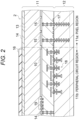
- Fig. 2 is a cross-sectional view of the imaging device 1 according to the present embodiment.
- the imaging device 1 according to the present embodiment is obtained by bonding a first substrate 11 and a second substrate 12 together using Cu-Cu bonding, a via, a bump, or the like.
- the plurality of pixel circuits 2 is formed in a partial region (pixel region) 11a of the first substrate 11.
- the first substrate 11 has, for example, a photoelectric conversion region (photodiode) 13 formed by implanting and diffusing impurity ions into a floating zone (FZ) silicon substrate.
- the photoelectric conversion region 13 includes a cathode (n + cathode layer) 14 formed on an upper surface side and an anode (p + anode layer) 15 and a ground layer (GND) 10 formed on a lower surface side.
- An X-ray shielding plate 16 is arranged above a region (peripheral circuit region) 11b other than the pixel region 11a of the first substrate 11.
- a wiring layer 17 connected to the pixel circuit 2 and peripheral circuits 18 such as the DSF circuit 5, the S/H circuit 6, the ADC 7, and the IF circuit 9 which are illustrated in Fig. 1 , and a wiring circuit are formed on the second substrate 12 located below the X-ray shielding plate 16, a wiring layer 17 connected to the pixel circuit 2 and peripheral circuits 18 such as the DSF circuit 5, the S/H circuit 6, the ADC 7, and the IF circuit 9 which are illustrated in Fig. 1 , and a wiring circuit are formed.
- a guard ring 19 is arranged on a lower surface of the photoelectric conversion region 13 on the peripheral circuit region 11b side, and the cathode (n + cathode layer) 14 is formed on an outer peripheral side thereof.
- Fig. 3 is a circuit diagram illustrating an example of a specific circuit configuration of the pixel circuit 2 illustrated in Fig. 1 .
- Fig. 3 illustrates a circuit configuration of one pixel circuit 2.
- the pixel circuit 2 includes a conversion unit 21, a first capacitor C0, a second capacitor C1, a voltage buffer 22, a first storage unit 23, and a second storage unit 24.
- the pixel circuit 2 illustrated in Fig. 3 includes a plurality of transistors.
- Fig. 3 illustrates an example in which all of the plurality of transistors are configured using PMOS transistors, but may be configured using NMOS transistors.
- the conversion unit 21 is the photodiode 13 that converts an incident electromagnetic wave (X-ray) into a charge.
- the first capacitor C0 and the second capacitor C1 constitute a conversion capacitance C, and a charge according to the incident intensity of the X-ray is accumulated in at least one of the first capacitor C0 or the second capacitor C1.
- a voltage between both electrodes of each of the capacitors increases as the amount of the accumulated charge increases.
- the first capacitor C0 accumulates a charge when a voltage corresponding to the charge is equal to or lower than a predetermined threshold.
- the second capacitor C1 accumulates a charge when a voltage corresponding to the charge exceeds the threshold.
- the first capacitor C0 accumulates the charge when the incident intensity of the X-ray is not so high, and the second capacitor C1 starts accumulating the charge when the accumulated charge in the first capacitor C0 increases to some extent.
- the voltage buffer 22 is a voltage conversion circuit that converts the charges accumulated in the first capacitor C0 and the second capacitor C1 into voltages.
- the voltage buffer 22 includes a transistor Q3.
- a current source 25 is connected between a source of the transistor Q3 and the power supply voltage node.
- the anode of the photodiode 13, one end of the first capacitor C0, and one end of the second capacitor C1 are connected to a gate of the transistor Q3.
- the transistor Q3 has a drain connected to a ground node. A source voltage of the transistor Q3 changes according to the accumulated charges in the first capacitor C0 and the second capacitor C1.
- the first storage unit 23 stores a voltage corresponding to the accumulated charge in the first capacitor C0 after a lapse of a first period since the first capacitor C0 has started accumulating the charge.
- the first period is a period in one frame period.
- the first storage unit 23 includes, for example, a capacitor Cs1 and a transistor Q1.
- the capacitor Cs1 is connected between a drain of the transistor Q1 and a reference voltage node (for example, a ground node).
- a signal S1 is input to a gate of the transistor Q1.
- the second storage unit 24 stores a voltage corresponding to the accumulated charges in the first capacitor C0 and the second capacitor C1 after a lapse of a second period longer than the first period since the first capacitor C0 has started accumulating the charge.
- the second period is a period in one frame period.
- the second storage unit 24 includes, for example, a transistor Q2 and a capacitor Cs2.
- the capacitor Cs2 is connected between a drain of the transistor Q2 and the ground node.
- a signal S2 is input to a gate of the transistor Q2.
- the pixel circuit 2 may include a first voltage limiter 26.
- the first voltage limiter 26 blocks the accumulation of the charge in the second capacitor C1 in a case where the voltage corresponding to the charge is equal to or lower than the threshold, and accumulates the charge in the second capacitor C1 when the voltage exceeds the threshold.
- the first voltage limiter 26 includes, for example, a transistor Q6.
- a voltage V1 is input to a gate of the transistor Q6.
- a drain of the transistor Q6 is connected to one end of the second capacitor C1, and a source of the transistor Q6 is connected to the anode of the photodiode 13 and one end of the first capacitor C0. It is possible to control a voltage of the anode of the photodiode 13 at which the second capacitor C1 start accumulating the charge by controlling the gate voltage V1 of the transistor Q6.
- the pixel circuit 2 may include a third storage unit 27 and a fourth storage unit 28.
- the third storage unit 27 stores the voltage corresponding to the accumulated charge in the first capacitor C0 after the lapse of the first period since the first capacitor C0 has started accumulating the charge, which is similar to the first storage unit 23.
- the fourth storage unit 28 stores the voltage corresponding to the accumulated charges in the first capacitor C0 and the second capacitor C1 after the second period longer than the lapse of the first period since the first capacitor C0 has started accumulating the charge, which is similar to the second storage unit 24.
- the pixel circuit 2 can include: a first system unit 29 including the first storage unit 23 and the second storage unit 24; and a second system unit 30 including the third storage unit 27 and the fourth storage unit 28. Therefore, exposure results of a previous frame stored in the third storage unit 27 and the fourth storage unit 28 in the second system unit 30 can be output to the signal line VSL while the voltages corresponding to the charges accumulated in the first capacitor C0 and the second capacitor C1 by exposure are being stored in the first storage unit 23 and the second storage unit 24 in the first system unit 29, and furthermore, the voltages corresponding to the charges accumulated in the first capacitor C0 and the second capacitor C1 by exposure can be stored in the third storage unit 27 and the fourth storage unit 28 in the second system unit 30 while the voltages stored in the first storage unit 23 and the second storage unit 24 in the first system unit 29 are being output to the signal line VSL. Therefore, the pixel circuit 2 in Fig. 3 can perform the exposure in most of one frame period.
- the pixel circuit 2 may include a first reset circuit 31 and a fifth storage unit 32.
- the first reset circuit 31 discharges and initializes the accumulated charges in the first capacitor C0 and the second capacitor C1.
- the first reset circuit 31 includes, for example, a transistor Q4.
- a source of the transistor Q4 is connected to the anode of the photodiode 13, one end of the first capacitor C0, one end of the second capacitor C1, and the gate of the transistor Q6 in the voltage buffer 22.
- a drain of the transistor Q4 is connected to the ground node.
- the transistor Q4 is turned on to perform an initialization operation when a signal RST input to its gate is low.
- the fifth storage unit 32 stores an initialization voltage when the first capacitor C0 and the second capacitor C1 are initialized.
- the fifth storage unit 32 includes, for example, a transistor Q5 and a capacitor Ccds2. One end of the capacitor Ccds2 is connected to the drain of the transistor Q2, and another end of the capacitor Ccds2 is connected to a source of the transistor Q5. A drain of the transistor Q5 is connected to the ground node. A signal S4 is input to a gate of the transistor Q5.
- the pixel circuit 2 may include a first transfer circuit 33.
- the first transfer circuit 33 outputs a differential voltage between the voltage stored in the second storage unit 24 and the voltage stored in the fifth storage unit 32 to the signal line VSL every frame period.
- the first transfer circuit 33 includes, for example, cascode-connected transistors Q7 and Q8.
- the transistor Q7 has a source connected to an output node of the pixel circuit 2 and a drain connected to a source of the transistor Q8.
- a drain of the transistor Q8 is connected to the ground node.
- a signal SEL2 is input to a gate of the transistor Q7.
- a gate of the transistor Q8 is connected to the another end of the capacitor Ccds2 and the source of the transistor Q5.
- the pixel circuit 2 may include a sixth storage unit 34.
- the sixth storage unit 34 stores a voltage of a charge transfer path immediately after the initialization by the first reset circuit 31 is released.
- the sixth storage unit 34 stores kTC noise when the first reset circuit 31 releases reset.
- the sixth storage unit 34 includes, for example, a transistor Q9 and a capacitor Ccds1.
- the capacitor Ccds1 is connected between the drain of the transistor Q1 and a source of the transistor Q9.
- a drain of the transistor Q9 is connected to the ground node.
- a signal S3 is input to a gate of the transistor Q9.
- the pixel circuit 2 may include a second transfer circuit 35.
- the second transfer circuit 35 outputs a differential voltage between the voltage stored in the first storage unit 23 and the voltage stored in the sixth storage unit 34 to the signal line VSL every frame period.
- the second transfer circuit 35 includes, for example, cascode-connected transistors Q10 and Q11.
- a source of the transistor Q10 is connected to the output node of the pixel circuit 2.
- a drain of the transistor Q10 is connected to a source of the transistor Q11.
- a drain of the transistor Q11 is connected to the ground node.
- a signal SEL1 is input to the gate of a transistor Q10.
- a gate of the transistor Q11 is connected to another end of the capacitor Ccds1 and the source of the transistor Q9.
- the first system unit 29 in the pixel circuit 2 in Fig. 3 includes the transistors Q1, Q2, Q5, and Q7 to Q11 and the capacitors Cs1, Cs2, Ccds1, and Ccds2.
- the second system unit 30 having the same circuit configuration as the first system unit 29 includes transistors Q12 to Q19 and capacitors Cs3, Cs4, Ccds3, and Ccds4. As described above, the first system unit 29 and the second system unit 30 alternately perform exposure or voltage transfer to the signal line VSL in each frame period.
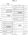
- Fig. 4 is a timing chart of the pixel circuit 2 of Fig. 3 .
- the operations of the pixel circuit 2 in Fig. 3 will be described with reference to Fig. 4 .
- the signal RST becomes low so that the transistor Q4 in the first reset circuit 31 is turned on, and the signal V1 is low so that the transistor Q6 in the first voltage limiter 26 is turned on. Therefore, the first capacitor C0 and the second capacitor C1 connected to both the sources of the transistors Q6 and Q4 discharge accumulated charges to be initialized.
- the signals S2 and S4 are low, and thus, the transistor Q2 in the second storage unit 24 and the transistor Q5 in the fifth storage unit 32 are turned on, and a charge according to a reset potential is accumulated in the capacitor Ccds2.
- the capacitor Ccds2 stores the reset potential obtained when the first reset circuit 31 has initialized the first capacitor C0 and the second capacitor C1.
- the gate voltage of the transistor Q6 in the first voltage limiter 26 is set to a voltage level Vm according to a gain switching mode.
- the gate voltage Vm of the transistor Q6 is set in advance such that the transistor Q6 is turned on when a certain amount or more of current flows through the anode of the photodiode 13 in order to operate the pixel circuit 2 in a mode (hereinafter, referred to as a two-gain mode) in which two gains can be switched.
- the transistor Q6 is turned on when the anode voltage of the photodiode 13 exceeds Vm + Vth.
- the gate voltage Vm at a high voltage level is set such that the transistor Q6 is always turned off in order to operate the pixel circuit 2 in a gain-fixed mode.
- the signal RST becomes high
- the transistor Q4 in the first reset circuit 31 is turned off, and reset is released.
- a charge photoelectrically converted by the photodiode 13 is accumulated in the first capacitor C0, and a charge is also accumulated in the capacitor Cs1 according to the accumulated charge.
- the signal S1 becomes high so that the transistor Q1 in the first storage unit 23 is turned off. Therefore, a voltage corresponding to the accumulated charge in the first capacitor C0 is stored in the capacitor Cs1 in the first storage unit 23.
- An exposure time period using the first capacitor C0 is between the time t5 and the time t6.
- a gain in a case where exposure is performed using only the first capacitor C0 is referred to as a high conversion gain C0.
- the gate voltage of the transistor Q6 in the first voltage limiter 26 is lowered, the transistor Q6 is completely turned on, and both the first capacitor C0 and the second capacitor C1 accumulate the charge from the photodiode 13.
- the signal S2 becomes high so that the transistor Q2 in the second storage unit 24 is turned off. Therefore, a voltage corresponding to the accumulated charges in the first capacitor C0 and the second capacitor C1 is accumulated in the capacitor Cs2 in the second storage unit 24.
- An exposure time period using the first capacitor C0 and the second capacitor C1 is between the time t4 and a time t8.
- a gain in a case where exposure is performed using the first capacitor C0 and the second capacitor C1 is referred to as a low conversion gain (C0 + C1).
- the transistor Q6 When the anode voltage of the photodiode 13 becomes Vm + Vth, the transistor Q6 is turned on, and thus, a limit is applied at Vm + Vth.
- the gate voltage Vm of the transistor Q6 is appropriately set so that saturation of the pixel circuit 2 can be avoided. Furthermore, a dynamic range of the high conversion gain C0 can be secured until the anode voltage of the photodiode 13 becomes Vm + Vth.
- the voltage with the high conversion gain C0 and the voltage with the low conversion gain (C0 + C1) can be obtained for the exposure time periods having substantially the same length, and the dynamic range can be expanded.
- S/N is important, and thus, noise can be reduced by offsetting the kTC noise at the time of reset, and one photon of an X-ray can be accurately detected.
- the first system unit 29 of the pixel circuit 2 in Fig. 3 performs an exposure operation
- the second system unit 30 outputs voltages stored in the third storage unit 27 and the fourth storage unit 28 by exposure in a previous frame to the signal line VSL during the exposure operation.
- the transistor Q18 is turned on at the time t1, and the voltage obtained by subtracting kTC noise stored in the capacitor Ccds3 from a voltage, photoelectrically converted with the high conversion gain C0 in the previous frame and stored in the capacitor Cs3 in the third storage unit 27, is output to the signal line VSL.
- the second system unit 30 performs exposure, and the voltages stored in the first storage unit 23 and the second storage unit 24 in the previous frame (the time t1 to the time t8) by the first system unit 29 are output to the signal line VSL. More specifically, at a time t9, a voltage of a charge transfer path at the time of reset is stored in the capacitor Ccds4. Thereafter, at a time t11, a voltage of kTC noise is stored in the capacitor Ccds3. Thereafter, the voltage with the high conversion gain C0 is stored in the capacitor Cs3 at a time t13. Thereafter, a voltage with the low conversion gain (C0 + C1) is stored in the capacitor Cs4 at the time t15.
- the transistor Q10 in the first system unit 29 is turned on at the time t8, and outputs a voltage, obtained by subtracting the voltage of the kTC noise stored in the capacitor Ccds1 from the voltage stored in the capacitor Cs1 with the high conversion gain C0, to the signal line VSL.
- the transistor Q7 is turned on after a time t12, and outputs a voltage, obtained by subtracting a reset voltage stored in the capacitor Ccds2 from the voltage stored in the capacitor Cs2 with the low conversion gain (C0 + C1), to the signal line VSL.
- Fig. 5 is a block diagram illustrating a configuration of the imaging device 1 on the subsequent stage side of the signal line VSL.
- the plurality of signal lines VSL is arranged in the horizontal direction X, and a plurality of the pixel circuits 2 is connected to each of the signal lines VSL. Voltages output from the plurality of pixel circuits 2 in one frame are sequentially sent to the signal line VSL.
- the plurality of signal lines VSL transfers the voltages respectively output from the pixel circuits 2 in parallel at the same time.
- the DSF circuit 5 is connected to each of the signal lines VSL.
- the DSF circuit 5 operates once in one frame and sets a potential of the corresponding signal line VSL to the reference potential. Therefore, the reference potential of the comparator in the ADC 7 is set.
- the voltage of each of the signal lines VSL is sampled and held by the S/H circuit 6 before being subjected to AD conversion in the ADC 7.
- an imaging size of each pixel is large, and a length of the signal line VSL connected to the pixel circuit 2 is about 5 cm, for example.
- the S/H circuit is provided on the preceding stage side of the ADC 7 to shorten time for the settling of a signal line voltage on the signal line VSL in the present embodiment.
- the voltage of each of the signal lines VSL is sampled and held by the S/H circuit 6 every predetermined period.
- the respective pixel circuits 2 output the voltage with the high conversion gain C0 and the voltage with the low conversion gain (C0 + C1) to each of the signal lines VSL with time shifted, and these voltages are sequentially sampled and held by the S/H circuit 6.
- the ADC 7 includes a comparator 41, a ramp wave selector 42, and a counter 43.
- the comparator 41 compares the sampled and held signal line voltage with a ramp wave voltage.
- Two types of ramp wave voltages and a reference voltage Vref are input to the ADC 7 of Fig. 5 .
- these two types of ramp wave voltages are referred to as a coarse ramp wave voltage (Coarse_ramp or first ramp wave voltage) and a fine ramp wave voltage (Fine_ramp or second ramp wave voltage).
- the fine ramp wave voltage has a smaller change width of a voltage amplitude and a lower voltage change rate over time than the coarse ramp wave voltage.
- the comparator 41 compares the signal line voltage with the coarse ramp wave voltage or the fine ramp wave voltage, and the counter 43 counts a period from the sampling and holding time to a time when the signal line voltage intersects the coarse ramp wave voltage or the fine ramp wave voltage.
- a count value of the counter 43 is a digital signal obtained by performing AD conversion of the signal line voltage.
- the logic circuit 8 includes a first multiplexer (MUX) 44, a determination circuit 45, a first holding circuit (Latch 1) 46, a second holding circuit (Latch 2) 47, and a second multiplexer (MUX) 48.
- MUX multiplexer
- the first multiplexer 44 divides and outputs the digital signal output from the counter 43 into two systems in parallel.
- the determination circuit 45 determines which digital signal of the high conversion gain C0 and the low conversion gain (C0 + C1) is to be output. The determination circuit 45 determines to output the digital signal of the low conversion gain (C0 + C1) when the digital signal of the high conversion gain is saturated, and determines to output the digital signal of the high conversion gain C0 when the digital signal of the high conversion gain is not saturated.
- the first holding circuit 46 or the second holding circuit 47 latches the digital signal on the basis of a determination result in the determination circuit 45.
- a free holding circuit is selected from the first holding circuit 46 and the second holding circuit 47 to latch the digital signal.
- the digital signals latched by the first holding circuit 46 and the second holding circuit 47 are sent to the IF circuit 9 via the second multiplexer 48.
- the second multiplexer 48 controls whether or not to send the digital signals latched by the first holding circuit 46 and the second holding circuit 47 to the IF circuit 9 on the basis of a determination result of the determination circuit 45.
- the IF circuit 9 outputs the digital signal latched by the first holding circuit 46 or the second holding circuit 47 to the outside.
- the determination circuit 45 as illustrated in Fig. 5 is provided to output only a valid digital signal, the imaging operation of the imaging device 1 can be speeded up.
- the HG/LG discriminator 49 can discriminate whether the digital signal has the high conversion gain C0 or the low conversion gain (C0 + C1), add 1 bit to a result of the discrimination, and outputs a digital signal having (n + 1) bits from the IF circuit 9. Therefore, either the digital signal of the high conversion gain C0 or the digital signal of the low conversion gain (C0 + C1) can be easily identified.
- the signal line voltage with the high conversion gain C0 and the signal line voltage with the low conversion gain (C0 + C1) output from the respective pixel circuits 2 are sequentially transferred in one frame period.
- the signal line voltage with the high conversion gain C0 and the signal line voltage with the low conversion gain (C0 + C1) output from the respective pixel circuits 2 are sequentially transferred in one frame period.
- the ADC 7 performs AD conversion eight times in one frame period.
- the exposure operation can be performed in most of one frame period even if the AD conversion is performed a plurality of times in the one frame period.
- the determination circuit 45 in the logic circuit 8 illustrated in Fig. 5 is not an essential configuration, and may be omitted. Furthermore, the first holding circuit 46 and the second holding circuit 47 are provided in the logic circuit 8 in Fig. 5 , but only one holding circuit may be provided.
- Fig. 6 is a timing chart of the ADC 7 and the logic circuit 8 in a case where the logic circuit 8 does not include the determination circuit 45 but includes only one holding circuit.
- Fig. 6 illustrates timings of digital signals output from the ACD 7, timings of latch transfer pulses input to the holding circuit, timings of latch output signals of the holding circuit, and transfer timings of the logic circuit 8.
- Fig. 6 illustrates an example in which four pixel circuits 2 (pixel circuits #1 to #4 in Fig. 6 ) are connected to one signal line VSL.
- the ADC 7 performs Auto Zero with the reference potential of the signal line VSL set by the DSF circuit 5 to set the reference potential of the comparator 41, thereafter, performs AD conversion on the signal line voltage (HG in Fig. 6 ) with the high conversion gain C0 output from each of the pixel circuits 2, and subsequently performs AD conversion on the signal line voltage (LG in Fig. 6 ) with the low conversion gain (C0 + C1).
- Such a series of operations is repeated for each of the four pixel circuits 2.
- the ADC 7 performs AD conversion for a total of eight pixels in one frame period.
- the holding circuit in the logic circuit 8 sequentially latches the digital signals for the eight pixels output from the ADC 7.
- a cycle in which the holding circuit holds each of the digital signals is 1/9 of one frame period.
- Fig. 7 is a timing chart of the ADC 7 and the logic circuit 8 in a case where the logic circuit 8 includes the determination circuit 45, the first holding circuit 46, and the second holding circuit 47.
- Fig. 7 illustrates timings of digital signals output from the ACD 7, timings of latch transfer pulses input to the first holding circuit 46 and the second holding circuit 47, timings of latch output signals (Latch 1) of the first holding circuit 46, a timing of latch output signals (Latch 2) of the second holding circuit 47, and transfer timings of the logic circuit 8.
- the ADC 7 performs AD conversion for eight pixels in one frame period and allocates the digital signals after subjected the AD conversion to the first holding circuit 46 and the second holding circuit 47, so that the logic circuit 8 only needs to transfer data for one pixel in 2/9 frame period. Therefore, there is a time margin for the processing of the logic circuit 8, and a frame rate can be further improved accordingly.
- the pixel circuit 2 in Fig. 3 can switch between the high conversion gain C0 and the low conversion gain (C0 + C1), a mode of fixing a gain to the high conversion gain C0 or the low conversion gain (C0 + C1) may be provided.
- the gain is fixed, an imaging speed can be improved.
- Fig. 8 is a timing chart of the ADC 7 and the logic circuit 8 in a case where a gain of the pixel circuit 2 is fixed and the logic circuit 8 is provided with one holding circuit.
- the ADC 7 since the ADC 7 is only required to perform AD conversion for four pixels in one frame period, the ADC 7 only needs to perform AD conversion for one pixel in 1/5 frame period. Therefore, since the number of times of the AD conversion of the ADC 7 is smaller than that in the case of Fig. 6 , the frame rate can be improved accordingly.
- Fig. 9 is a timing chart in a case where a gain of the pixel circuit 2 is fixed and the logic circuit 8 is provided with the first holding circuit 46 and the second holding circuit 47.
- the logic circuit 8 is only required to transfer digital data of each pixel in 1/4 frame period, the frame rate can be improved as compared with the cases of Figs. 6 to 8 .
- Fig. 10 is a detailed timing chart illustrating operations of the imaging device 1 according to the present embodiment.
- the S/H circuit 6 samples and holds the signal line voltage.
- the signal line voltage is low, and thus, the comparator 41 selects the fine ramp wave voltage.
- the fine ramp wave voltage is indicated by a solid line
- the coarse ramp wave voltage is indicated by an alternate long and short dash line.
- the comparator 41 in the ADC 7 compares the sampled and held signal voltage with the fine ramp wave voltage, and the counter 43 performs a counting operation from the time t1 to a time t1a at which the sampled and held signal voltage intersects the fine ramp wave voltage, and outputs a count value obtained at a time t1a as a digital signal.
- the second holding circuit 47 latches the digital signal. Therefore, the IF circuit 9 outputs the digital signal latched by the second holding circuit 47 after the time t1b.
- an auto-zero period in which the DSF circuit 5 sets the signal line VSL to the reference potential is started.
- the S/H circuit 6 samples and holds the reference potential of the signal line VSL. Since the sampled and held signal line voltage is at the reference potential level, the fine ramp wave voltage is selected.
- the ADC 7 sets the reference potential of the comparator 41 and does not perform a normal AD conversion operation.
- the S/H circuit 6 samples and holds a signal line voltage #1HG with a high gain conversion C0 of the pixel circuit #1. Since the sampled and held signal line voltage is higher than the reference voltage Vref, the coarse ramp wave voltage is selected. Since the sampled and held signal line voltage intersects the coarse ramp wave voltage at a time t3a, the counter 43 in the ADC 7 outputs a count value obtained from the time t3 to the time t3a as a digital signal. At the subsequent time t3b, the first holding circuit 46 latches the digital signal.
- the S/H circuit 6 samples and holds a signal line voltage #1LG with a low gain conversion (C0 + C1) of the pixel circuit 2 #1. Since the sampled and held signal line voltage is equal to or lower than the reference voltage Vref, the fine ramp wave voltage is selected. Since the sampled and held signal line voltage intersects the fine ramp wave voltage at a time t4a, the counter 43 in the ADC 7 outputs a count value obtained from the time t4 to the time t4a as a digital signal. At the subsequent time t4b, the second holding circuit 47 latches the digital signal.
- the determination circuit 45 determines that the digital signal #1HG with the high conversion gain C0 latched in the first holding circuit 46 is not saturated. Therefore, the IF circuit 9 outputs the digital signal #1HG held in the first holding circuit 46 at the time t4b.
- the determination circuit 45 determines that a digital signal #2HG with the high conversion gain C0 latched in the second holding circuit 47 is saturated. Therefore, the IF circuit 9 outputs the digital signal #2MG of the low conversion gain (C0 + C1) latched in the first holding circuit 46 at the time t6b.
- the first capacitor C0 for the high conversion gain and the second capacitor C1 for the low conversion gain are provided in the pixel circuit 2 in the first embodiment in this manner, it is possible to selectively use the first capacitor C0 and the second capacitor C1 in accordance with the intensity of an electromagnetic wave such as an X-ray incident on the photodiode 13 to store charges. Therefore, even if a strong electromagnetic wave is incident on the photodiode 13, the intensity of the electromagnetic wave can be accurately detected without causing saturation.
- the exposure operation can be performed in most of one frame period, and dead time in which the electromagnetic wave is not receivable can be reduced.
- the reset potential when the first reset circuit 31 has been reset is stored, the kTC noise generated when the first reset circuit 31 has released the reset is stored, and the reset potential and the kTC noise are offset when the voltage is output to the signal line VSL, and thus, an S/N ratio can be improved particularly when a weak electromagnetic wave is imaged.
- a second embodiment provides an HDR mode for further expanding a dynamic range.
- a pixel circuit in an imaging device has a circuit configuration similar to that in Fig. 3 .
- the pixel circuit according to the second embodiment includes the HDR mode in addition to a high conversion gain mode and a low conversion gain mode described in the first embodiment.
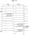
- Fig. 11 is a timing chart of the pixel circuit according to the second embodiment.
- Fig. 11 in one frame (Frame N) of two adjacent frames, exposure with the high conversion gain and exposure with the low conversion gain are performed by substantially the same length, and voltages with the respective gains are output to a signal line.
- an exposure time period with the low conversion gain is made shorter than an exposure time period with the high conversion gain, and voltages with the respective gains are output to the signal line.
- the timing chart of Fig. 11 assumes a situation where an X-ray dose does not change during each frame period.
- the X-ray dose does not change over one frame period
- a ratio of the exposure time period/frame period with the high conversion gain is increased such that the single photon can be reliably detected, and the dynamic range can be further expanded by shortening the exposure time period with the low conversion gain.
- an equivalent frame rate is 1/2 of a normal frame rate.
- a pixel irradiated with a strong X-ray and a pixel irradiated with only one photon may occur at the same time.
- the exposure time period with the high conversion gain is set to a duty ratio of 90% or more of a total time period of two frames.
- the low conversion gain is selected. In the example of Fig.
- imaging data of the low conversion gain LG of Frame N is used as long as the X-ray dose is at an unsaturated level.
- imaging data of a short exposure time period with the low conversion gain LG in Frame (N + 1) is used.
- the signal S8 becomes high at a time t2, and the transistor Q14 is turned off.
- the exposure operation with the low conversion gain is started from a time point when reset is released at the subsequent time t3.
- the signal RST becomes low at a time t4 so that charges in the capacitors C0 and C1 are reset, and the signal RST becomes high at a time t5 so that the transistor Q4 is turned off, and the exposure operation with the low conversion gain is started from this time point.
- a length of a first period (HG detection period) can be made shorter and accumulated charge amounts in the first capacitor C0 and the second capacitor C1 can be limited as compared with another frame period (for example, a period of Frame N in Fig. 11 ). That is, in the one frame period, the accumulated charges in the first capacitor C0 and the second capacitor C1 are temporarily discharged before the first period (HG detection period) elapses and a second period (LG detection period) elapses after the first capacitor C0 and the second capacitor C1 have started the charge accumulation, and thereafter, the charge accumulation is resumed.
- a voltage corresponding to the accumulated charge in the first capacitor C0 is stored in the third storage unit 27 after the lapse of the first period, and a voltage corresponding to the accumulated charges in the first capacitor C0 and the second capacitor C1 is stored in the fourth storage unit 28 after the lapse of the second period.
- the voltage corresponding to the accumulated charge in the first capacitor C0 may be stored in the first storage unit 23 after the lapse of the first period in the one frame period described above, and the voltage corresponding to the accumulated charges in the first capacitor C0 and the second capacitor C1 may be stored in the fourth storage unit 28 after the lapse of the second period.
- the HDR mode is newly provided in the second embodiment in this manner, a weak X-ray can be reliably detected, and accurate detection can be performed without saturation even in a case where a strong X-ray is emitted, and the dynamic range can be further expanded.
Landscapes
- Engineering & Computer Science (AREA)
- Multimedia (AREA)
- Signal Processing (AREA)
- Physics & Mathematics (AREA)
- Health & Medical Sciences (AREA)
- Life Sciences & Earth Sciences (AREA)
- General Physics & Mathematics (AREA)
- High Energy & Nuclear Physics (AREA)
- Molecular Biology (AREA)
- Spectroscopy & Molecular Physics (AREA)
- Transforming Light Signals Into Electric Signals (AREA)
- Studio Devices (AREA)
- Solid State Image Pick-Up Elements (AREA)
Abstract
Description
- The present disclosure relates to an imaging device.
- In an imaging device that images an electromagnetic wave such as incident radiation, low noise performance, a high speed, and a high dynamic range are required.
Patent Document 1 discloses an X-ray detector provided with an integration capacitor to perform reading of a signal and an integration operation of the integration capacitor in parallel.Patent Document 2 discloses a computer tomograph that determines a gain of a next frame on the basis of an output value in a current frame by using a fact that a variation between the frames is not large.Patent Document 3 discloses a radiation image pickup system in which a noise output line is added, and voltage values with a high conversion gain and a low conversion gain are stored in a pixel. -
- Patent Document 1:
Japanese Patent Application Laid-Open No. 2013-503325 - Patent Document 2:
Japanese Patent Application Laid-Open No. 2002-533691 - Patent Document 3:
Japanese Patent Application Laid-Open No. 2016-82255 - In the X-ray detector of
Patent Document 1, the integration capacitor has a fixed capacitance, and is saturated at a high dose, and there is a problem that a dose of X-rays is not correctly detectable. - The tomograph of
Patent Document 2 can switch a capacitance of the feedback capacitor, but it is difficult to cope with a sudden variation in an input signal because a feedback capacitance of the next frame is selected from the current output value. Furthermore, a feedback amplifier is used, and thus, there is a problem for a high-speed operation. - The radiation image pickup system of
Patent Document 3 is provided with a selector switch for "wide", but a circuit is saturated so that a charge as a signal disappears if a high dose is input before switching the switch. Furthermore, there is a restriction on an exposure time period in one frame. - In view of the above problems of the related art, the present disclosure provides an imaging device with low noise, a high speed, and a high dynamic range.
- In order to solve the above problems, according to the present disclosure, there is provided an imaging device including:
- a conversion unit that converts an incident electromagnetic wave into a charge;
- a first capacitor that accumulates the charge when a voltage corresponding to the charge is equal to or lower than a predetermined threshold;
- a second capacitor that accumulates the charge when the voltage exceeds the threshold;
- a voltage conversion circuit that converts the charges accumulated in the first capacitor and the second capacitor into voltages;
- a first storage unit that stores a voltage corresponding to the accumulated charge in the first capacitor after a lapse of a first period since the first capacitor has started accumulating the charge; and
- a second storage unit that stores a voltage corresponding to the accumulated charges in the first capacitor and the second capacitor after a lapse of a second period longer than the first period since the first capacitor has started accumulating the charge.
- A third storage unit that stores a voltage corresponding to the accumulated charge in the first capacitor after a lapse of the first period since the first capacitor has started accumulating the charge and
- a fourth storage unit that stores a voltage corresponding to the accumulated charges in the first capacitor and the second capacitor after the lapse of the second period since the first capacitor has started accumulating the charge may be further provided
- such that voltages stored in the third storage unit and the fourth storage unit in a frame period immediately before a predetermined frame period are output to a signal line while storing corresponding voltages respectively in the first storage unit and the second storage unit in the predetermined frame period, and
- the voltages stored in the first storage unit and the second storage unit in the predetermined frame period are output to the signal line while storing corresponding voltages in the third storage unit and the fourth storage unit in a frame period immediately after the predetermined frame period.
- A first reset circuit that discharges the accumulated charges in the first capacitor and the second capacitor for initialization and
a fifth storage unit that stores an initialization voltage when the first capacitor and the second capacitor are initialized may be further provided. - A first transfer circuit that outputs a differential voltage between the voltage stored in the second storage unit and the voltage stored in the fifth storage unit to a signal line every frame period may be further provided.
- A sixth storage unit that stores a voltage of a path connected to the first reset circuit when the initialization by the first reset circuit is released may be further provided.
- A second transfer circuit that outputs a differential voltage between the voltage stored in the first storage unit and the voltage stored in the sixth storage unit to a signal line every frame period may be further provided.
- A first voltage limiter that blocks the accumulation of the charge in the second capacitor in a case where the voltage corresponding to the charge is equal to or lower than the threshold, and accumulates the charge in the second capacitor in a case where the voltage exceeds the threshold may be further provided.
- A mode selection unit that selects whether to store a voltage corresponding to the accumulated charge of one of the first capacitor and the second capacitor in the second storage unit or to store a voltage corresponding to the accumulated charges of the first capacitor and the second capacitor in the second storage unit may be further provided.
- A sample and hold circuit that samples and holds a voltage of a signal line that sequentially transfers the voltages stored in the first storage unit and the second storage unit at a predetermined cycle and
an AD converter that converts the voltage sampled and held by the sample and hold circuit into a digital signal may be further provided. - A first holding circuit that holds one voltage out of the voltage stored in the first storage unit and the voltage stored in the second storage unit and
a second holding circuit that holds another voltage out of the voltage stored in the first storage unit and the voltage stored in the second storage unit may be further provided. - A determination circuit that determines whether or not the accumulated charge in the first capacitor is saturated on the basis of digital signals held in the first holding circuit and the second holding circuit and
a selection circuit that selects and outputs the digital signal held in the first holding circuit or the second holding circuit on the basis of a determination result of the determination circuit may be further provided. - The AD converter may include:
- a ramp wave selector that selects a first ramp wave voltage when the voltage held in the sample and hold circuit is equal to or higher than a predetermined reference voltage, and selects a second ramp wave voltage having a smaller change width of a voltage amplitude and a lower voltage change rate over time than the first ramp wave voltage when the voltage held in the sample and hold circuit is lower than the reference voltage;
- a comparison unit that compares the voltage held in the sample and hold circuit with the first ramp wave voltage or the second ramp wave voltage; and
- a counter that generates the digital signal on the basis of a comparison result of the comparison unit.
- A plurality of pixel circuits connected to the signal line may be further provided
- such that the pixel circuit includes the conversion unit, the first capacitor, the second capacitor, the first storage unit, and the second storage unit, and
- the sample and hold circuit sequentially holds voltages output from the plurality of pixel circuits in one frame period.
- A mode selection unit capable of selecting a predetermined mode for expanding a dynamic range may be further provided
such that, when the predetermined mode is selected, in one frame period out of two successive frame periods, a length of the first period is shortened as compared with length of the first period in another frame period, and an amount of the accumulated charges of the first capacitor and the second capacitor stored in the second storage unit is limited. - In the one frame period, the accumulated charges in the first capacitor and the second capacitor may be temporarily discharged before the first period elapses and the second period elapses after the first capacitor and the second capacitor have started the charge accumulation, and thereafter, the accumulation of the charges may be resumed, and
the second storage unit may store a voltage corresponding to accumulated charges after the first capacitor and the second capacitor resume the charge accumulation in the one frame period. - A mode selection unit capable of selecting a predetermined mode for expanding a dynamic range may be further provided
such that, when the predetermined mode is selected, in one frame period out of two successive frame periods, a length of the first period is shortened as compared with length of the first period in another frame period, and an amount of the accumulated charges of the first capacitor and the second capacitor stored in the second storage unit and the fourth storage unit is limited. - In the one frame period, the accumulated charges in the first capacitor and the second capacitor may be temporarily discharged before the first period elapses and the second period elapses after the first capacitor and the second capacitor have started the charge accumulation, and thereafter, the accumulation of the charges may be resumed, and
the fourth storage unit may store a voltage corresponding to accumulated charges after the first capacitor and the second capacitor resume the charge accumulation in the one frame period. -
-
Fig. 1 is a block diagram illustrating a schematic configuration of an imaging device according to a first embodiment. -
Fig. 2 is a cross-sectional view of the imaging device according to the present embodiment. -
Fig. 3 is a circuit diagram illustrating an example of a specific circuit configuration of a pixel circuit illustrated inFig. 1 . -
Fig. 4 is a timing chart of the pixel circuit ofFig. 3 . -
Fig. 5 is a block diagram illustrating a configuration of the imaging device on the subsequent stage side of a signal line. -
Fig. 6 is a timing chart of an ADC and a logic circuit in a case where the logic circuit does not include a determination circuit but includes only one holding circuit. -
Fig. 7 is a timing chart of the ADC and the logic circuit in a case where the logic circuit includes the determination circuit, a first holding circuit, and a second holding circuit. -
Fig. 8 is a timing chart of the ADC and the logic circuit in a case where a gain of the pixel circuit is fixed and the logic circuit is provided with one holding circuit. -
Fig. 9 is a timing chart in a case where the gain of the pixel circuit is fixed and the logic circuit is provided with the first holding circuit and the second holding circuit. -
Fig. 10 is a detailed timing chart illustrating operations of the imaging device according to the present embodiment. -
Fig. 11 is a timing chart of a pixel circuit according to a second embodiment. - Hereinafter, embodiments of an imaging device will be described with reference to the drawings. Although the following description will be given focusing on main constituent portions of the imaging device will be mainly described, the imaging device may have constituent portions and functions that are not illustrated or described. The following description does not exclude the constituent portions or functions that are not illustrated or described.
-
Fig. 1 is a block diagram illustrating a schematic configuration of animaging device 1 according to a first embodiment. Theimaging device 1 ofFig. 1 images an electromagnetic wave in a predetermined frequency band. Although the imaging device 1 (also referred to as an X-ray detection device) that detects an X-ray will be described as a specific example hereinafter, the present embodiment is also applicable to a frequency band other than X-rays. - The
imaging device 1 ofFig. 1 includes apixel array unit 1a and aperipheral circuit unit 1b. Thepixel array unit 1a includes a plurality ofpixel circuits 2 arranged in a horizontal direction X and a vertical direction Y, a plurality of signal lines VSL extending in the vertical direction Y, and a plurality of scanning lines (not illustrated) extending in the horizontal direction X. Theperipheral circuit unit 1b includes a scanning line drive circuit (V_Driver) 4, a dummy source follower circuit (hereinafter, DSF circuit) 5, a sample and hold circuit (hereinafter, S/H circuit) 6, an analog-to-digital conversion circuit (hereinafter, ADC) 7, alogic circuit 8, and an interface circuit (IF circuit) 9. - In the
imaging device 1 ofFig. 1 , the number of thepixel circuits 2 and the number of the signal lines VSL are freely set. Thepixel array unit 1a and theperipheral circuit unit 1b may be formed on the same substrate, or at least a part of theperipheral circuit unit 1b may be formed on a substrate different from a formation substrate of thepixel array unit 1a as described later. - The
pixel circuit 2 includes a photodiode and a read circuit. Specific configurations and operations of thepixel circuit 2 will be described later. The plurality ofpixel circuits 2 arranged in the vertical direction Y is connected to the plurality of signal lines VSL. More specifically, a plurality of thepixel circuits 2 arranged at intervals in the vertical direction is connected to one signal line VSL. Each of the signal lines VSL transfers an imaging signal imaged by the plurality ofpixel circuits 2 in one frame. - The
DSF circuit 5 sets a reference potential of a comparator in theADC 7 as described later. The S/H circuit 6 cyclically samples and holds voltages of the respective signal lines VSL. TheADC 7 converts the sampled and held voltages into digital signals. Thelogic circuit 8 sequentially holds the AD-converted digital signals. TheIF circuit 9 outputs the digital signals held in thelogic circuit 8. -
Fig. 2 is a cross-sectional view of theimaging device 1 according to the present embodiment. As illustrated inFig. 2 , theimaging device 1 according to the present embodiment is obtained by bonding afirst substrate 11 and asecond substrate 12 together using Cu-Cu bonding, a via, a bump, or the like. The plurality ofpixel circuits 2 is formed in a partial region (pixel region) 11a of thefirst substrate 11. Thefirst substrate 11 has, for example, a photoelectric conversion region (photodiode) 13 formed by implanting and diffusing impurity ions into a floating zone (FZ) silicon substrate. Thephotoelectric conversion region 13 includes a cathode (n+ cathode layer) 14 formed on an upper surface side and an anode (p+ anode layer) 15 and a ground layer (GND) 10 formed on a lower surface side. - An
X-ray shielding plate 16 is arranged above a region (peripheral circuit region) 11b other than thepixel region 11a of thefirst substrate 11. On thesecond substrate 12 located below theX-ray shielding plate 16, awiring layer 17 connected to thepixel circuit 2 andperipheral circuits 18 such as theDSF circuit 5, the S/H circuit 6, theADC 7, and theIF circuit 9 which are illustrated inFig. 1 , and a wiring circuit are formed. Aguard ring 19 is arranged on a lower surface of thephotoelectric conversion region 13 on theperipheral circuit region 11b side, and the cathode (n+ cathode layer) 14 is formed on an outer peripheral side thereof. -
Fig. 3 is a circuit diagram illustrating an example of a specific circuit configuration of thepixel circuit 2 illustrated inFig. 1 .Fig. 3 illustrates a circuit configuration of onepixel circuit 2. As illustrated inFig. 3 , thepixel circuit 2 includes aconversion unit 21, a first capacitor C0, a second capacitor C1, avoltage buffer 22, afirst storage unit 23, and asecond storage unit 24. Thepixel circuit 2 illustrated inFig. 3 includes a plurality of transistors.Fig. 3 illustrates an example in which all of the plurality of transistors are configured using PMOS transistors, but may be configured using NMOS transistors. - The
conversion unit 21 is thephotodiode 13 that converts an incident electromagnetic wave (X-ray) into a charge. The first capacitor C0 and the second capacitor C1 constitute a conversion capacitance C, and a charge according to the incident intensity of the X-ray is accumulated in at least one of the first capacitor C0 or the second capacitor C1. In the first capacitor C0 and the second capacitor C1, a voltage between both electrodes of each of the capacitors increases as the amount of the accumulated charge increases. The first capacitor C0 accumulates a charge when a voltage corresponding to the charge is equal to or lower than a predetermined threshold. The second capacitor C1 accumulates a charge when a voltage corresponding to the charge exceeds the threshold. - In this manner, the first capacitor C0 accumulates the charge when the incident intensity of the X-ray is not so high, and the second capacitor C1 starts accumulating the charge when the accumulated charge in the first capacitor C0 increases to some extent.
- The
voltage buffer 22 is a voltage conversion circuit that converts the charges accumulated in the first capacitor C0 and the second capacitor C1 into voltages. Thevoltage buffer 22 includes a transistor Q3. Acurrent source 25 is connected between a source of the transistor Q3 and the power supply voltage node. The anode of thephotodiode 13, one end of the first capacitor C0, and one end of the second capacitor C1 are connected to a gate of the transistor Q3. The transistor Q3 has a drain connected to a ground node. A source voltage of the transistor Q3 changes according to the accumulated charges in the first capacitor C0 and the second capacitor C1. - The
first storage unit 23 stores a voltage corresponding to the accumulated charge in the first capacitor C0 after a lapse of a first period since the first capacitor C0 has started accumulating the charge. In the present embodiment, it is assumed that exposure and voltage transfer to the signal line VSL are performed in one frame period, and the first period is a period in one frame period. - The
first storage unit 23 includes, for example, a capacitor Cs1 and a transistor Q1. The capacitor Cs1 is connected between a drain of the transistor Q1 and a reference voltage node (for example, a ground node). A signal S1 is input to a gate of the transistor Q1. - The
second storage unit 24 stores a voltage corresponding to the accumulated charges in the first capacitor C0 and the second capacitor C1 after a lapse of a second period longer than the first period since the first capacitor C0 has started accumulating the charge. The second period is a period in one frame period. - The
second storage unit 24 includes, for example, a transistor Q2 and a capacitor Cs2. The capacitor Cs2 is connected between a drain of the transistor Q2 and the ground node. A signal S2 is input to a gate of the transistor Q2. - As illustrated in
Fig. 3 , thepixel circuit 2 according to the present embodiment may include afirst voltage limiter 26. Thefirst voltage limiter 26 blocks the accumulation of the charge in the second capacitor C1 in a case where the voltage corresponding to the charge is equal to or lower than the threshold, and accumulates the charge in the second capacitor C1 when the voltage exceeds the threshold. Thefirst voltage limiter 26 includes, for example, a transistor Q6. A voltage V1 is input to a gate of the transistor Q6. A drain of the transistor Q6 is connected to one end of the second capacitor C1, and a source of the transistor Q6 is connected to the anode of thephotodiode 13 and one end of the first capacitor C0. It is possible to control a voltage of the anode of thephotodiode 13 at which the second capacitor C1 start accumulating the charge by controlling the gate voltage V1 of the transistor Q6. - As illustrated in
Fig. 3 , thepixel circuit 2 according to the present embodiment may include athird storage unit 27 and afourth storage unit 28. Thethird storage unit 27 stores the voltage corresponding to the accumulated charge in the first capacitor C0 after the lapse of the first period since the first capacitor C0 has started accumulating the charge, which is similar to thefirst storage unit 23. - The
fourth storage unit 28 stores the voltage corresponding to the accumulated charges in the first capacitor C0 and the second capacitor C1 after the second period longer than the lapse of the first period since the first capacitor C0 has started accumulating the charge, which is similar to thesecond storage unit 24. - As illustrated in
Fig. 3 , thepixel circuit 2 according to the present embodiment can include: afirst system unit 29 including thefirst storage unit 23 and thesecond storage unit 24; and asecond system unit 30 including thethird storage unit 27 and thefourth storage unit 28. Therefore, exposure results of a previous frame stored in thethird storage unit 27 and thefourth storage unit 28 in thesecond system unit 30 can be output to the signal line VSL while the voltages corresponding to the charges accumulated in the first capacitor C0 and the second capacitor C1 by exposure are being stored in thefirst storage unit 23 and thesecond storage unit 24 in thefirst system unit 29, and furthermore, the voltages corresponding to the charges accumulated in the first capacitor C0 and the second capacitor C1 by exposure can be stored in thethird storage unit 27 and thefourth storage unit 28 in thesecond system unit 30 while the voltages stored in thefirst storage unit 23 and thesecond storage unit 24 in thefirst system unit 29 are being output to the signal line VSL. Therefore, thepixel circuit 2 inFig. 3 can perform the exposure in most of one frame period. - As illustrated in
Fig. 3 , thepixel circuit 2 according to the present embodiment may include afirst reset circuit 31 and afifth storage unit 32. Thefirst reset circuit 31 discharges and initializes the accumulated charges in the first capacitor C0 and the second capacitor C1. Thefirst reset circuit 31 includes, for example, a transistor Q4. A source of the transistor Q4 is connected to the anode of thephotodiode 13, one end of the first capacitor C0, one end of the second capacitor C1, and the gate of the transistor Q6 in thevoltage buffer 22. A drain of the transistor Q4 is connected to the ground node. The transistor Q4 is turned on to perform an initialization operation when a signal RST input to its gate is low. - The
fifth storage unit 32 stores an initialization voltage when the first capacitor C0 and the second capacitor C1 are initialized. Thefifth storage unit 32 includes, for example, a transistor Q5 and a capacitor Ccds2. One end of the capacitor Ccds2 is connected to the drain of the transistor Q2, and another end of the capacitor Ccds2 is connected to a source of the transistor Q5. A drain of the transistor Q5 is connected to the ground node. A signal S4 is input to a gate of the transistor Q5. - As illustrated in
Fig. 3 , thepixel circuit 2 according to the present embodiment may include afirst transfer circuit 33. Thefirst transfer circuit 33 outputs a differential voltage between the voltage stored in thesecond storage unit 24 and the voltage stored in thefifth storage unit 32 to the signal line VSL every frame period. Thefirst transfer circuit 33 includes, for example, cascode-connected transistors Q7 and Q8. The transistor Q7 has a source connected to an output node of thepixel circuit 2 and a drain connected to a source of the transistor Q8. A drain of the transistor Q8 is connected to the ground node. A signal SEL2 is input to a gate of the transistor Q7. A gate of the transistor Q8 is connected to the another end of the capacitor Ccds2 and the source of the transistor Q5. - As illustrated in
Fig. 3 , thepixel circuit 2 according to the present embodiment may include asixth storage unit 34. Thesixth storage unit 34 stores a voltage of a charge transfer path immediately after the initialization by thefirst reset circuit 31 is released. Thesixth storage unit 34 stores kTC noise when thefirst reset circuit 31 releases reset. Thesixth storage unit 34 includes, for example, a transistor Q9 and a capacitor Ccds1. The capacitor Ccds1 is connected between the drain of the transistor Q1 and a source of the transistor Q9. A drain of the transistor Q9 is connected to the ground node. A signal S3 is input to a gate of the transistor Q9. - As illustrated in
Fig. 3 , thepixel circuit 2 according to the present embodiment may include asecond transfer circuit 35. Thesecond transfer circuit 35 outputs a differential voltage between the voltage stored in thefirst storage unit 23 and the voltage stored in thesixth storage unit 34 to the signal line VSL every frame period. Thesecond transfer circuit 35 includes, for example, cascode-connected transistors Q10 and Q11. A source of the transistor Q10 is connected to the output node of thepixel circuit 2. A drain of the transistor Q10 is connected to a source of the transistor Q11. A drain of the transistor Q11 is connected to the ground node. A signal SEL1 is input to the gate of a transistor Q10. A gate of the transistor Q11 is connected to another end of the capacitor Ccds1 and the source of the transistor Q9. - In this manner, the
first system unit 29 in thepixel circuit 2 inFig. 3 includes the transistors Q1, Q2, Q5, and Q7 to Q11 and the capacitors Cs1, Cs2, Ccds1, and Ccds2. Furthermore, thesecond system unit 30 having the same circuit configuration as thefirst system unit 29 includes transistors Q12 to Q19 and capacitors Cs3, Cs4, Ccds3, and Ccds4. As described above, thefirst system unit 29 and thesecond system unit 30 alternately perform exposure or voltage transfer to the signal line VSL in each frame period. -
Fig. 4 is a timing chart of thepixel circuit 2 ofFig. 3 . Hereinafter, the operations of thepixel circuit 2 inFig. 3 will be described with reference toFig. 4 . - First, at a time t1, the signal RST becomes low so that the transistor Q4 in the
first reset circuit 31 is turned on, and the signal V1 is low so that the transistor Q6 in thefirst voltage limiter 26 is turned on. Therefore, the first capacitor C0 and the second capacitor C1 connected to both the sources of the transistors Q6 and Q4 discharge accumulated charges to be initialized. At this time, the signals S2 and S4 are low, and thus, the transistor Q2 in thesecond storage unit 24 and the transistor Q5 in thefifth storage unit 32 are turned on, and a charge according to a reset potential is accumulated in the capacitor Ccds2. - Thereafter, at a time t2, the signal S4 becomes high so that the transistor Q5 is turned off. Therefore, the capacitor Ccds2 stores the reset potential obtained when the
first reset circuit 31 has initialized the first capacitor C0 and the second capacitor C1. - Thereafter, at a time t3, the gate voltage of the transistor Q6 in the
first voltage limiter 26 is set to a voltage level Vm according to a gain switching mode. For example, the gate voltage Vm of the transistor Q6 is set in advance such that the transistor Q6 is turned on when a certain amount or more of current flows through the anode of thephotodiode 13 in order to operate thepixel circuit 2 in a mode (hereinafter, referred to as a two-gain mode) in which two gains can be switched. In this case, the transistor Q6 is turned on when the anode voltage of thephotodiode 13 exceeds Vm + Vth. On the other hand, the gate voltage Vm at a high voltage level is set such that the transistor Q6 is always turned off in order to operate thepixel circuit 2 in a gain-fixed mode. - Thereafter, at a time t4, the signal RST becomes high, the transistor Q4 in the
first reset circuit 31 is turned off, and reset is released. After the time t4, a charge photoelectrically converted by thephotodiode 13 is accumulated in the first capacitor C0, and a charge is also accumulated in the capacitor Cs1 according to the accumulated charge. - Thereafter, at a time t5, the signal S3 becomes high, the transistor Q9 in the
sixth storage unit 34 is turned off, and kTC noise generated when thefirst reset circuit 31 has released the reset is stored in the capacitor Ccds1. - Thereafter, at a time t6, the signal S1 becomes high so that the transistor Q1 in the
first storage unit 23 is turned off. Therefore, a voltage corresponding to the accumulated charge in the first capacitor C0 is stored in the capacitor Cs1 in thefirst storage unit 23. An exposure time period using the first capacitor C0 is between the time t5 and the time t6. Hereinafter, a gain in a case where exposure is performed using only the first capacitor C0 is referred to as a high conversion gain C0. - At a time t7, the gate voltage of the transistor Q6 in the
first voltage limiter 26 is lowered, the transistor Q6 is completely turned on, and both the first capacitor C0 and the second capacitor C1 accumulate the charge from thephotodiode 13. - Thereafter, at a time t8, the signal S2 becomes high so that the transistor Q2 in the
second storage unit 24 is turned off. Therefore, a voltage corresponding to the accumulated charges in the first capacitor C0 and the second capacitor C1 is accumulated in the capacitor Cs2 in thesecond storage unit 24. An exposure time period using the first capacitor C0 and the second capacitor C1 is between the time t4 and a time t8. Hereinafter, a gain in a case where exposure is performed using the first capacitor C0 and the second capacitor C1 is referred to as a low conversion gain (C0 + C1). - When the anode voltage of the
photodiode 13 becomes Vm + Vth, the transistor Q6 is turned on, and thus, a limit is applied at Vm + Vth. Thus, the gate voltage Vm of the transistor Q6 is appropriately set so that saturation of thepixel circuit 2 can be avoided. Furthermore, a dynamic range of the high conversion gain C0 can be secured until the anode voltage of thephotodiode 13 becomes Vm + Vth. - When the anode voltage of the
photodiode 13 exceeds Vm + Vth, the charge from thephotodiode 13 is accumulated in the second capacitor C1, and thus, there is no possibility that the charge from thephotodiode 13 disappears. The transistor Q6 in thefirst voltage limiter 26 is completely turned on at the time t7, the charges accumulated in the first capacitor C0 and the second capacitor C1 can be converted into a voltage with the low conversion gain (C0 + C1). - In this manner, the voltage with the high conversion gain C0 and the voltage with the low conversion gain (C0 + C1) can be obtained for the exposure time periods having substantially the same length, and the dynamic range can be expanded. In a case where photoelectric conversion is performed with the high conversion gain C0, S/N is important, and thus, noise can be reduced by offsetting the kTC noise at the time of reset, and one photon of an X-ray can be accurately detected.
- From the time t1 to the time t8 in
Fig. 4 , for example, thefirst system unit 29 of thepixel circuit 2 inFig. 3 performs an exposure operation, and thesecond system unit 30 outputs voltages stored in thethird storage unit 27 and thefourth storage unit 28 by exposure in a previous frame to the signal line VSL during the exposure operation. More specifically, the transistor Q18 is turned on at the time t1, and the voltage obtained by subtracting kTC noise stored in the capacitor Ccds3 from a voltage, photoelectrically converted with the high conversion gain C0 in the previous frame and stored in the capacitor Cs3 in thethird storage unit 27, is output to the signal line VSL. Thereafter, at the time t5, the voltage obtained by subtracting a reset potential stored in the capacitor Ccds4 at the time of reset from a voltage, stored in the capacitor Cs4 in thefourth storage unit 28 with the low conversion gain (C0 + C1) in the previous frame, is output to the signal line VSL. - Thereafter, in the next frame illustrated from the time t8 to a time t15, the
second system unit 30 performs exposure, and the voltages stored in thefirst storage unit 23 and thesecond storage unit 24 in the previous frame (the time t1 to the time t8) by thefirst system unit 29 are output to the signal line VSL. More specifically, at a time t9, a voltage of a charge transfer path at the time of reset is stored in the capacitor Ccds4. Thereafter, at a time t11, a voltage of kTC noise is stored in the capacitor Ccds3. Thereafter, the voltage with the high conversion gain C0 is stored in the capacitor Cs3 at a time t13. Thereafter, a voltage with the low conversion gain (C0 + C1) is stored in the capacitor Cs4 at the time t15. - Furthermore, while the
second system unit 30 is performing the exposure from the time t8 to the time t15, the transistor Q10 in thefirst system unit 29 is turned on at the time t8, and outputs a voltage, obtained by subtracting the voltage of the kTC noise stored in the capacitor Ccds1 from the voltage stored in the capacitor Cs1 with the high conversion gain C0, to the signal line VSL. Furthermore, the transistor Q7 is turned on after a time t12, and outputs a voltage, obtained by subtracting a reset voltage stored in the capacitor Ccds2 from the voltage stored in the capacitor Cs2 with the low conversion gain (C0 + C1), to the signal line VSL. -
Fig. 5 is a block diagram illustrating a configuration of theimaging device 1 on the subsequent stage side of the signal line VSL. The plurality of signal lines VSL is arranged in the horizontal direction X, and a plurality of thepixel circuits 2 is connected to each of the signal lines VSL. Voltages output from the plurality ofpixel circuits 2 in one frame are sequentially sent to the signal line VSL. The plurality of signal lines VSL transfers the voltages respectively output from thepixel circuits 2 in parallel at the same time. - The
DSF circuit 5 is connected to each of the signal lines VSL. TheDSF circuit 5 operates once in one frame and sets a potential of the corresponding signal line VSL to the reference potential. Therefore, the reference potential of the comparator in theADC 7 is set. - The voltage of each of the signal lines VSL is sampled and held by the S/
H circuit 6 before being subjected to AD conversion in theADC 7. In X-ray imaging, an imaging size of each pixel is large, and a length of the signal line VSL connected to thepixel circuit 2 is about 5 cm, for example. Thus, even if a certain pixel is selected to output a voltage, it takes time to perform settling with a time constant due to a resistance or capacitance of the signal line VSL, and thus, the number of times AD conversion can be performed in one frame decreases. Therefore, the S/H circuit is provided on the preceding stage side of theADC 7 to shorten time for the settling of a signal line voltage on the signal line VSL in the present embodiment. - The voltage of each of the signal lines VSL is sampled and held by the S/
H circuit 6 every predetermined period. Therespective pixel circuits 2 output the voltage with the high conversion gain C0 and the voltage with the low conversion gain (C0 + C1) to each of the signal lines VSL with time shifted, and these voltages are sequentially sampled and held by the S/H circuit 6. - The
ADC 7 includes acomparator 41, aramp wave selector 42, and acounter 43. Thecomparator 41 compares the sampled and held signal line voltage with a ramp wave voltage. Two types of ramp wave voltages and a reference voltage Vref are input to theADC 7 ofFig. 5 . Hereinafter, these two types of ramp wave voltages are referred to as a coarse ramp wave voltage (Coarse_ramp or first ramp wave voltage) and a fine ramp wave voltage (Fine_ramp or second ramp wave voltage). The fine ramp wave voltage has a smaller change width of a voltage amplitude and a lower voltage change rate over time than the coarse ramp wave voltage. Thecomparator 41 and theramp wave selector 42 in theADC 7 ofFig. 5 compare the sampled and held signal line voltage with the reference voltage Vref, select the coarse ramp wave voltage when the signal line voltage is higher than the reference voltage Vref, and select the fine ramp wave voltage when the signal line voltage is equal to or lower than the reference voltage Vref. - The
comparator 41 compares the signal line voltage with the coarse ramp wave voltage or the fine ramp wave voltage, and the counter 43 counts a period from the sampling and holding time to a time when the signal line voltage intersects the coarse ramp wave voltage or the fine ramp wave voltage. A count value of thecounter 43 is a digital signal obtained by performing AD conversion of the signal line voltage. - The
logic circuit 8 includes a first multiplexer (MUX) 44, adetermination circuit 45, a first holding circuit (Latch 1) 46, a second holding circuit (Latch 2) 47, and a second multiplexer (MUX) 48. - The
first multiplexer 44 divides and outputs the digital signal output from thecounter 43 into two systems in parallel. - The
determination circuit 45 determines which digital signal of the high conversion gain C0 and the low conversion gain (C0 + C1) is to be output. Thedetermination circuit 45 determines to output the digital signal of the low conversion gain (C0 + C1) when the digital signal of the high conversion gain is saturated, and determines to output the digital signal of the high conversion gain C0 when the digital signal of the high conversion gain is not saturated. - The
first holding circuit 46 or thesecond holding circuit 47 latches the digital signal on the basis of a determination result in thedetermination circuit 45. A free holding circuit is selected from thefirst holding circuit 46 and thesecond holding circuit 47 to latch the digital signal. The digital signals latched by thefirst holding circuit 46 and thesecond holding circuit 47 are sent to theIF circuit 9 via thesecond multiplexer 48. Thesecond multiplexer 48 controls whether or not to send the digital signals latched by thefirst holding circuit 46 and thesecond holding circuit 47 to theIF circuit 9 on the basis of a determination result of thedetermination circuit 45. - The
IF circuit 9 outputs the digital signal latched by thefirst holding circuit 46 or thesecond holding circuit 47 to the outside. - Since the
pixel circuits 2 sequentially output the voltage with the high conversion gain C0 and the voltage with the low conversion gain (C0 + C1) to the signal line VSL, the number of digital signals to be output is too large if thelogic circuit 8 outputs all of the digital signal corresponding to the voltage with the high conversion gain C0 and the digital signal corresponding to the voltage with the low conversion gain (C0 + C1) output from all thepixel circuits 2, which becomes a factor of deterioration in an imaging operation of theimaging device 1. Thus, thedetermination circuit 45 as illustrated inFig. 5 is provided to output only a valid digital signal, the imaging operation of theimaging device 1 can be speeded up. - Furthermore, when a digital signal output from the
counter 43 has n bits, the HG/LG discriminator 49 can discriminate whether the digital signal has the high conversion gain C0 or the low conversion gain (C0 + C1), add 1 bit to a result of the discrimination, and outputs a digital signal having (n + 1) bits from theIF circuit 9. Therefore, either the digital signal of the high conversion gain C0 or the digital signal of the low conversion gain (C0 + C1) can be easily identified. - As illustrated in
Fig. 5 , since the plurality ofpixel circuits 2 is connected to one signal line VSL, the signal line voltage with the high conversion gain C0 and the signal line voltage with the low conversion gain (C0 + C1) output from therespective pixel circuits 2 are sequentially transferred in one frame period. For example, in a case where fourpixel circuits 2 are connected to one signal line VSL, eight (2 × 4 = 8) signal line voltages are transferred by the signal line VSL in one frame period, and theADC 7 performs AD conversion eight times in one frame period. - Since the
first system unit 29 and thesecond system unit 30 alternately perform the exposure and the AD conversion in one frame period as illustrated inFig. 4 in the present embodiment, the exposure operation can be performed in most of one frame period even if the AD conversion is performed a plurality of times in the one frame period. - The
determination circuit 45 in thelogic circuit 8 illustrated inFig. 5 is not an essential configuration, and may be omitted. Furthermore, thefirst holding circuit 46 and thesecond holding circuit 47 are provided in thelogic circuit 8 inFig. 5 , but only one holding circuit may be provided. -
Fig. 6 is a timing chart of theADC 7 and thelogic circuit 8 in a case where thelogic circuit 8 does not include thedetermination circuit 45 but includes only one holding circuit.Fig. 6 illustrates timings of digital signals output from theACD 7, timings of latch transfer pulses input to the holding circuit, timings of latch output signals of the holding circuit, and transfer timings of thelogic circuit 8. -
Fig. 6 illustrates an example in which four pixel circuits 2 (pixel circuits # 1 to #4 inFig. 6 ) are connected to one signal line VSL. At the beginning of one frame period, theADC 7 performs Auto Zero with the reference potential of the signal line VSL set by theDSF circuit 5 to set the reference potential of thecomparator 41, thereafter, performs AD conversion on the signal line voltage (HG inFig. 6 ) with the high conversion gain C0 output from each of thepixel circuits 2, and subsequently performs AD conversion on the signal line voltage (LG inFig. 6 ) with the low conversion gain (C0 + C1). Such a series of operations is repeated for each of the fourpixel circuits 2. Eventually, theADC 7 performs AD conversion for a total of eight pixels in one frame period. The holding circuit in thelogic circuit 8 sequentially latches the digital signals for the eight pixels output from theADC 7. A cycle in which the holding circuit holds each of the digital signals is 1/9 of one frame period. -
Fig. 7 is a timing chart of theADC 7 and thelogic circuit 8 in a case where thelogic circuit 8 includes thedetermination circuit 45, thefirst holding circuit 46, and thesecond holding circuit 47.Fig. 7 illustrates timings of digital signals output from theACD 7, timings of latch transfer pulses input to thefirst holding circuit 46 and thesecond holding circuit 47, timings of latch output signals (Latch 1) of thefirst holding circuit 46, a timing of latch output signals (Latch 2) of thesecond holding circuit 47, and transfer timings of thelogic circuit 8. - As described above, the
ADC 7 performs AD conversion for eight pixels in one frame period and allocates the digital signals after subjected the AD conversion to thefirst holding circuit 46 and thesecond holding circuit 47, so that thelogic circuit 8 only needs to transfer data for one pixel in 2/9 frame period. Therefore, there is a time margin for the processing of thelogic circuit 8, and a frame rate can be further improved accordingly. - Although the
pixel circuit 2 inFig. 3 can switch between the high conversion gain C0 and the low conversion gain (C0 + C1), a mode of fixing a gain to the high conversion gain C0 or the low conversion gain (C0 + C1) may be provided. When the gain is fixed, an imaging speed can be improved. -
Fig. 8 is a timing chart of theADC 7 and thelogic circuit 8 in a case where a gain of thepixel circuit 2 is fixed and thelogic circuit 8 is provided with one holding circuit. In this case, since theADC 7 is only required to perform AD conversion for four pixels in one frame period, theADC 7 only needs to perform AD conversion for one pixel in 1/5 frame period. Therefore, since the number of times of the AD conversion of theADC 7 is smaller than that in the case ofFig. 6 , the frame rate can be improved accordingly. -
Fig. 9 is a timing chart in a case where a gain of thepixel circuit 2 is fixed and thelogic circuit 8 is provided with thefirst holding circuit 46 and thesecond holding circuit 47. In the case ofFig. 9 , thelogic circuit 8 is only required to transfer digital data of each pixel in 1/4 frame period, the frame rate can be improved as compared with the cases ofFigs. 6 to 8 . -
Fig. 10 is a detailed timing chart illustrating operations of theimaging device 1 according to the present embodiment. The timing chart ofFig. 10 illustrates an example in which eightpixel circuits 2 are connected to one signal line VSL, and therespective pixel circuits 2 sequentially output data of the high conversion gain C0 and data of the low conversion gain (C0 + C1) to the signal line VSL. Since therespective pixel circuits 2 output two signal line voltages and theDSF circuit 5 sets a signal line voltage to a reference potential at the head of each frame period, a total of 1 + 8 + 8 = 17 signal line voltages are transferred through one signal line VSL in one frame period. - At a time t1, the S/
H circuit 6 samples and holds the signal line voltage. At this time point, the signal line voltage is low, and thus, thecomparator 41 selects the fine ramp wave voltage. InFig. 10 , the fine ramp wave voltage is indicated by a solid line, and the coarse ramp wave voltage is indicated by an alternate long and short dash line. Thecomparator 41 in theADC 7 compares the sampled and held signal voltage with the fine ramp wave voltage, and thecounter 43 performs a counting operation from the time t1 to a time t1a at which the sampled and held signal voltage intersects the fine ramp wave voltage, and outputs a count value obtained at a time t1a as a digital signal. Thereafter, at a time t1b, thesecond holding circuit 47 latches the digital signal. Therefore, theIF circuit 9 outputs the digital signal latched by thesecond holding circuit 47 after the time t1b. - At the time t1b, an auto-zero period (AZ period) in which the
DSF circuit 5 sets the signal line VSL to the reference potential is started. At a time t2, the S/H circuit 6 samples and holds the reference potential of the signal line VSL. Since the sampled and held signal line voltage is at the reference potential level, the fine ramp wave voltage is selected. Between the time t2 and a time t3, theADC 7 sets the reference potential of thecomparator 41 and does not perform a normal AD conversion operation. - At the time t3, the S/
H circuit 6 samples and holds a signal line voltage #1HG with a high gain conversion C0 of thepixel circuit # 1. Since the sampled and held signal line voltage is higher than the reference voltage Vref, the coarse ramp wave voltage is selected. Since the sampled and held signal line voltage intersects the coarse ramp wave voltage at a time t3a, thecounter 43 in theADC 7 outputs a count value obtained from the time t3 to the time t3a as a digital signal. At the subsequent time t3b, thefirst holding circuit 46 latches the digital signal. - Thereafter, at a time t4, the S/
H circuit 6 samples and holds a signal line voltage #1LG with a low gain conversion (C0 + C1) of thepixel circuit 2 #1. Since the sampled and held signal line voltage is equal to or lower than the reference voltage Vref, the fine ramp wave voltage is selected. Since the sampled and held signal line voltage intersects the fine ramp wave voltage at a time t4a, thecounter 43 in theADC 7 outputs a count value obtained from the time t4 to the time t4a as a digital signal. At the subsequent time t4b, thesecond holding circuit 47 latches the digital signal. - The
determination circuit 45 determines that the digital signal #1HG with the high conversion gain C0 latched in thefirst holding circuit 46 is not saturated. Therefore, theIF circuit 9 outputs the digital signal #1HG held in thefirst holding circuit 46 at the time t4b. - On the other hand, at the subsequent time t6b, the
determination circuit 45 determines that a digital signal #2HG with the high conversion gain C0 latched in thesecond holding circuit 47 is saturated. Therefore, theIF circuit 9 outputs the digital signal #2MG of the low conversion gain (C0 + C1) latched in thefirst holding circuit 46 at the time t6b. - Since the first capacitor C0 for the high conversion gain and the second capacitor C1 for the low conversion gain are provided in the
pixel circuit 2 in the first embodiment in this manner, it is possible to selectively use the first capacitor C0 and the second capacitor C1 in accordance with the intensity of an electromagnetic wave such as an X-ray incident on thephotodiode 13 to store charges. Therefore, even if a strong electromagnetic wave is incident on thephotodiode 13, the intensity of the electromagnetic wave can be accurately detected without causing saturation. - Furthermore, since the
first system unit 29 and thesecond system unit 30 are provided in thepixel circuit 2 and the exposure operation and the AD conversion operation are alternately performed, the exposure operation can be performed in most of one frame period, and dead time in which the electromagnetic wave is not receivable can be reduced. - Moreover, since the two types of ramp wave voltages are provided in order to perform the AD conversion operation, it is possible to quickly and accurately perform the AD conversion of the intensity of the electromagnetic wave received by the
photodiode 13. - Furthermore, the reset potential when the
first reset circuit 31 has been reset is stored, the kTC noise generated when thefirst reset circuit 31 has released the reset is stored, and the reset potential and the kTC noise are offset when the voltage is output to the signal line VSL, and thus, an S/N ratio can be improved particularly when a weak electromagnetic wave is imaged. - A second embodiment provides an HDR mode for further expanding a dynamic range.
- A pixel circuit in an imaging device according to the second embodiment has a circuit configuration similar to that in
Fig. 3 . The pixel circuit according to the second embodiment includes the HDR mode in addition to a high conversion gain mode and a low conversion gain mode described in the first embodiment. -
Fig. 11 is a timing chart of the pixel circuit according to the second embodiment. InFig. 11 , in one frame (Frame N) of two adjacent frames, exposure with the high conversion gain and exposure with the low conversion gain are performed by substantially the same length, and voltages with the respective gains are output to a signal line. In another frame (Frame N+1), an exposure time period with the low conversion gain is made shorter than an exposure time period with the high conversion gain, and voltages with the respective gains are output to the signal line. - In
Fig. 11 , the high conversion gain is denoted by HG, and the low conversion gain is denoted by LG. - The timing chart of
Fig. 11 assumes a situation where an X-ray dose does not change during each frame period. In a case where the X-ray dose does not change over one frame period, there is a possibility that charges accumulated in the first and second capacitors C0 and C1 are saturated. Therefore, an exposure time period is shortened only for the low conversion gain in one frame of the two frames. Therefore, an equivalent dynamic range can be expanded. For example, if an exposure time period with the low conversion gain is shortened to 1/10 of an exposure time period with the high conversion gain, the dynamic range becomes 10 times although the amount of received light does not change. - In the HDR mode, a ratio of the exposure time period/frame period with the high conversion gain is increased such that the single photon can be reliably detected, and the dynamic range can be further expanded by shortening the exposure time period with the low conversion gain.
- In the HDR mode, exposure and an AD conversion operation are performed in units of two successive frames. Thus, an equivalent frame rate is 1/2 of a normal frame rate. In X-ray irradiation, a pixel irradiated with a strong X-ray and a pixel irradiated with only one photon may occur at the same time. In the pixel irradiated with only one photon, it is desirable to extend an exposure time period as much as possible in order to capture the one photon. For example, the exposure time period with the high conversion gain is set to a duty ratio of 90% or more of a total time period of two frames. On the other hand, in the pixel irradiated with the strong X-ray, the low conversion gain is selected. In the example of
Fig. 11 , since the exposure time period with the low conversion gain LG is slightly longer than the exposure time period with the high conversion gain HG in the N-th frame, imaging data of the low conversion gain LG of Frame N is used as long as the X-ray dose is at an unsaturated level. On the other hand, in a case where the X-ray dose with the low conversion gain LG in Frame N is saturated, imaging data of a short exposure time period with the low conversion gain LG in Frame (N + 1) is used. - In a mode other than the HDR mode, the signal S8 becomes high at a time t2, and the transistor Q14 is turned off. Thus, the exposure operation with the low conversion gain is started from a time point when reset is released at the subsequent time t3. On the other hand, in the HDR mode, the signal RST becomes low at a time t4 so that charges in the capacitors C0 and C1 are reset, and the signal RST becomes high at a time t5 so that the transistor Q4 is turned off, and the exposure operation with the low conversion gain is started from this time point.
- More specifically, in the HDR mode, in one frame period (for example, a period of Frame (N + 1) in
Fig. 11 ) of two successive frame periods, a length of a first period (HG detection period) can be made shorter and accumulated charge amounts in the first capacitor C0 and the second capacitor C1 can be limited as compared with another frame period (for example, a period of Frame N inFig. 11 ). That is, in the one frame period, the accumulated charges in the first capacitor C0 and the second capacitor C1 are temporarily discharged before the first period (HG detection period) elapses and a second period (LG detection period) elapses after the first capacitor C0 and the second capacitor C1 have started the charge accumulation, and thereafter, the charge accumulation is resumed. A voltage corresponding to the accumulated charge in the first capacitor C0 is stored in thethird storage unit 27 after the lapse of the first period, and a voltage corresponding to the accumulated charges in the first capacitor C0 and the second capacitor C1 is stored in thefourth storage unit 28 after the lapse of the second period. Note that the voltage corresponding to the accumulated charge in the first capacitor C0 may be stored in thefirst storage unit 23 after the lapse of the first period in the one frame period described above, and the voltage corresponding to the accumulated charges in the first capacitor C0 and the second capacitor C1 may be stored in thefourth storage unit 28 after the lapse of the second period. - Since the HDR mode is newly provided in the second embodiment in this manner, a weak X-ray can be reliably detected, and accurate detection can be performed without saturation even in a case where a strong X-ray is emitted, and the dynamic range can be further expanded.
- Note that the present technology can have the following configurations.
- (1) An imaging device including:
- a conversion unit that converts an incident electromagnetic wave into a charge;
- a first capacitor that accumulates the charge when a voltage corresponding to the charge is equal to or lower than a predetermined threshold;
- a second capacitor that accumulates the charge when the voltage exceeds the threshold;
- a voltage conversion circuit that converts the charges accumulated in the first capacitor and the second capacitor into voltages;
- a first storage unit that stores a voltage corresponding to the accumulated charge in the first capacitor after a lapse of a first period since the first capacitor has started accumulating the charge; and
- a second storage unit that stores a voltage corresponding to the accumulated charges in the first capacitor and the second capacitor after a lapse of a second period longer than the first period since the first capacitor has started accumulating the charge.
- (2) The imaging device according to (1), further including:
- a third storage unit that stores a voltage corresponding to the accumulated charge in the first capacitor after a lapse of the first period since the first capacitor has started accumulating the charge; and
- a fourth storage unit that stores a voltage corresponding to the accumulated charges in the first capacitor and the second capacitor after the lapse of the second period since the first capacitor has started accumulating the charge,
- in which voltages stored in the third storage unit and the fourth storage unit in a frame period immediately before a predetermined frame period are output to a signal line while storing corresponding voltages respectively in the first storage unit and the second storage unit in the predetermined frame period, and
- the voltages stored in the first storage unit and the second storage unit in the predetermined frame period are output to the signal line while storing corresponding voltages in the third storage unit and the fourth storage unit in a frame period immediately after the predetermined frame period.
- (3) The imaging device according to (1) or (2), further including:
- a first reset circuit that discharges the accumulated charges in the first capacitor and the second capacitor for initialization; and
- a fifth storage unit that stores an initialization voltage when the first capacitor and the second capacitor are initialized.
- (4) The imaging device according to (3), further including a first transfer circuit that outputs a differential voltage between the voltage stored in the second storage unit and the voltage stored in the fifth storage unit to a signal line every frame period.
- (5) The imaging device according to (3) or (4), further including a sixth storage unit that stores a voltage of a path connected to the first reset circuit when the initialization by the first reset circuit is released.
- (6) The imaging device according to (5), further including a second transfer circuit that outputs a differential voltage between the voltage stored in the first storage unit and the voltage stored in the sixth storage unit to a signal line every frame period.
- (7) The imaging device according to any one of (1) to (6), further including a first voltage limiter that blocks the accumulation of the charge in the second capacitor in a case where the voltage corresponding to the charge is equal to or lower than the threshold, and accumulates the charge in the second capacitor in a case where the voltage exceeds the threshold.
- (8) The imaging device according to any one of (1) to (7), further including a mode selection unit that selects whether to store a voltage corresponding to the accumulated charge of one of the first capacitor and the second capacitor in the second storage unit or to store a voltage corresponding to the accumulated charges of the first capacitor and the second capacitor in the second storage unit.
- (9) The imaging device according to any one of (1) to (8), further including:
- a sample and hold circuit that samples and holds a voltage of a signal line that sequentially transfers the voltages stored in the first storage unit and the second storage unit at a predetermined cycle; and
- an AD converter that converts the voltage sampled and held by the sample and hold circuit into a digital signal.
- (10) The imaging device according to (9), further including:
- a first holding circuit that holds one voltage out of the voltage stored in the first storage unit and the voltage stored in the second storage unit; and
- a second holding circuit that holds another voltage out of the voltage stored in the first storage unit and the voltage stored in the second storage unit.
- (11) The imaging device according to (10), further including:
- a determination circuit that determines whether or not the accumulated charge in the first capacitor is saturated on the basis of digital signals held in the first holding circuit and the second holding circuit; and
- a selection circuit that selects and outputs the digital signal held in the first holding circuit or the second holding circuit on the basis of a determination result of the determination circuit.
- (12) The imaging device according to any one of (9) to (11), in which
the AD converter includes:- a ramp wave selector that selects a first ramp wave voltage when the voltage held in the sample and hold circuit is equal to or higher than a predetermined reference voltage, and selects a second ramp wave voltage having a smaller change width of a voltage amplitude and a lower voltage change rate over time than the first ramp wave voltage when the voltage held in the sample and hold circuit is lower than the reference voltage;
- a comparison unit that compares the voltage held in the sample and hold circuit with the first ramp wave voltage or the second ramp wave voltage; and
- a counter that generates the digital signal on the basis of a comparison result of the comparison unit.
- (13) The imaging device according to any one of (9) to (12), further including a plurality of pixel circuits connected to the signal line,
- in which the pixel circuit includes the conversion unit, the first capacitor, the second capacitor, the first storage unit, and the second storage unit, and
- the sample and hold circuit sequentially holds voltages output from the plurality of pixel circuits in one frame period.
- (14) The imaging device according to any one of (1) to (13), further including a mode selection unit capable of selecting a predetermined mode for expanding a dynamic range,
in which, when the predetermined mode is selected, in one frame period out of two successive frame periods, a length of the first period is shortened as compared with length of the first period in another frame period, and an amount of the accumulated charges of the first capacitor and the second capacitor stored in the second storage unit is limited. - (15) The imaging device according to (14), in which
- in the one frame period, the accumulated charges in the first capacitor and the second capacitor are temporarily discharged before the first period elapses and the second period elapses after the first capacitor and the second capacitor have started the charge accumulation, and thereafter, the accumulation of the charges is resumed, and
- the second storage unit stores a voltage corresponding to accumulated charges after the first capacitor and the second capacitor resume the charge accumulation in the one frame period.
- (16) The imaging device according to (2), further including a mode selection unit capable of selecting a predetermined mode for expanding a dynamic range,
in which, when the predetermined mode is selected, in one frame period out of two successive frame periods, a length of the first period is shortened as compared with length of the first period in another frame period, and an amount of the accumulated charges of the first capacitor and the second capacitor stored in the second storage unit and the fourth storage unit is limited. - (17) The imaging device according to (16), in which
- in the one frame period, the accumulated charges in the first capacitor and the second capacitor are temporarily discharged before the first period elapses and the second period elapses after the first capacitor and the second capacitor have started the charge accumulation, and thereafter, the accumulation of the charges is resumed, and
- the fourth storage unit stores a voltage corresponding to accumulated charges after the first capacitor and the second capacitor resume the charge accumulation in the one frame period.
- Aspects of the present disclosure are not limited to the above-described respective embodiments, but include various modifications that can be conceived by those skilled in the art, and effects of the present disclosure are not limited to the above-described contents. That is, various additions, changes, and partial deletions can be made within a scope not departing from a conceptual idea and a spirit of the present disclosure derived from the contents defined in the claims and equivalents thereof.
-
- 1
- Imaging device
- 1a
- Pixel array unit
- 1b
- Peripheral circuit unit
- 2
- Pixel circuit
- 4
- Scanning line drive circuit
- 5
- Dummy source follower circuit (DSF circuit)
- 6
- Sample and hold circuit (S/H circuit)
- 7
- Analog-to-digital conversion circuit (ADC)
- 8
- Logic circuit
- 9
- Interface circuit (IF circuit)
- 10
- Ground layer
- 11
- First substrate
- 12
- Second substrate
- 13
- Photoelectric conversion region (photodiode)
- 14
- Cathode
- 15
- Anode
- 16
- X-ray shielding plate
- 17
- Wiring layer
- 18
- Peripheral circuit
- 19
- Guard ring
- 21
- Conversion unit
- 22
- Voltage buffer
- 23
- First storage unit
- 24
- Second storage unit
- 25
- Current source
- 26
- First voltage limiter
- 27
- Third Storage unit
- 28
- Fourth storage unit
- 29
- First system unit
- 30
- Second system unit
- 31
- First reset circuit
- 32
- Fifth storage unit
- 33
- First transfer circuit
- 34
- Sixth storage unit
- 35
- Second transfer circuit
- 41
- Comparator
- 42
- Ramp wave selector
- 43
- Counter
- 44
- First multiplexer
- 45
- Determination circuit
- 46
- First holding circuit
- 47
- Second holding circuit
- 48
- Second multiplexer
- 49
- HG/LG discriminator
- 51
- Second voltage limiter
- 52
- Second reset circuit
- 53
- Gain switch
- C0
- First capacitor
- C1
- Second capacitor
- C2
- Third capacitor
Claims (17)
- An imaging device comprising:a conversion unit that converts an incident electromagnetic wave into a charge;a first capacitor that accumulates the charge when a voltage corresponding to the charge is equal to or lower than a predetermined threshold;a second capacitor that accumulates the charge when the voltage exceeds the threshold;a voltage conversion circuit that converts the charges accumulated in the first capacitor and the second capacitor into voltages;a first storage unit that stores a voltage corresponding to the accumulated charge in the first capacitor after a lapse of a first period since the first capacitor has started accumulating the charge; anda second storage unit that stores a voltage corresponding to the accumulated charges in the first capacitor and the second capacitor after a lapse of a second period longer than the first period since the first capacitor has started accumulating the charge.
- The imaging device according to claim 1, further comprising:a third storage unit that stores a voltage corresponding to the accumulated charge in the first capacitor after a lapse of the first period since the first capacitor has started accumulating the charge; anda fourth storage unit that stores a voltage corresponding to the accumulated charges in the first capacitor and the second capacitor after the lapse of the second period since the first capacitor has started accumulating the charge,wherein voltages stored in the third storage unit and the fourth storage unit in a frame period immediately before a predetermined frame period are output to a signal line while storing corresponding voltages respectively in the first storage unit and the second storage unit in the predetermined frame period, andthe voltages stored in the first storage unit and the second storage unit in the predetermined frame period are output to the signal line while storing corresponding voltages in the third storage unit and the fourth storage unit in a frame period immediately after the predetermined frame period.
- The imaging device according to claim 1, further comprising:a first reset circuit that discharges the accumulated charges in the first capacitor and the second capacitor for initialization; anda fifth storage unit that stores an initialization voltage when the first capacitor and the second capacitor are initialized.
- The imaging device according to claim 3, further comprising a first transfer circuit that outputs a differential voltage between the voltage stored in the second storage unit and the voltage stored in the fifth storage unit to a signal line every frame period.
- The imaging device according to claim 3, further comprising a sixth storage unit that stores a voltage of a path connected to the first reset circuit when the initialization by the first reset circuit is released.
- The imaging device according to claim 5, further comprising a second transfer circuit that outputs a differential voltage between the voltage stored in the first storage unit and the voltage stored in the sixth storage unit to a signal line every frame period.
- The imaging device according to claim 1, further comprising a first voltage limiter that blocks the accumulation of the charge in the second capacitor in a case where the voltage corresponding to the charge is equal to or lower than the threshold, and accumulates the charge in the second capacitor in a case where the voltage exceeds the threshold.
- The imaging device according to claim 1, further comprising a mode selection unit that selects whether to store a voltage corresponding to the accumulated charge of one of the first capacitor and the second capacitor in the second storage unit or to store a voltage corresponding to the accumulated charges of the first capacitor and the second capacitor in the second storage unit.
- The imaging device according to claim 1, further comprising:a sample and hold circuit that samples and holds a voltage of a signal line that sequentially transfers the voltages stored in the first storage unit and the second storage unit at a predetermined cycle; andan AD converter that converts the voltage sampled and held by the sample and hold circuit into a digital signal.
- The imaging device according to claim 9, further comprising:a first holding circuit that holds one voltage out of the voltage stored in the first storage unit and the voltage stored in the second storage unit; anda second holding circuit that holds another voltage out of the voltage stored in the first storage unit and the voltage stored in the second storage unit.
- The imaging device according to claim 10, further comprising:a determination circuit that determines whether or not the accumulated charge in the first capacitor is saturated on a basis of digital signals held in the first holding circuit and the second holding circuit; anda selection circuit that selects and outputs the digital signal held in the first holding circuit or the second holding circuit on a basis of a determination result of the determination circuit.
- The imaging device according to claim 9, wherein
the AD converter includes:a ramp wave selector that selects a first ramp wave voltage when the voltage held in the sample and hold circuit is equal to or higher than a predetermined reference voltage, and selects a second ramp wave voltage having a smaller change width of a voltage amplitude and a lower voltage change rate over time than the first ramp wave voltage when the voltage held in the sample and hold circuit is lower than the reference voltage;a comparison unit that compares the voltage held in the sample and hold circuit with the first ramp wave voltage or the second ramp wave voltage; anda counter that generates the digital signal on the basis of a comparison result of the comparison unit. - The imaging device according to claim 9, further comprising a plurality of pixel circuits connected to the signal line,wherein the pixel circuit includes the conversion unit, the first capacitor, the second capacitor, the first storage unit, and the second storage unit, andthe sample and hold circuit sequentially holds voltages output from the plurality of pixel circuits in one frame period.
- The imaging device according to claim 1, further comprising a mode selection unit capable of selecting a predetermined mode for expanding a dynamic range,
wherein, when the predetermined mode is selected, in one frame period out of two successive frame periods, a length of the first period is shortened as compared with a length of the first period in another frame period, and an amount of the accumulated charges of the first capacitor and the second capacitor stored in the second storage unit is limited. - The imaging device according to claim 14, whereinin the one frame period, the accumulated charges in the first capacitor and the second capacitor are temporarily discharged before the first period elapses and the second period elapses after the first capacitor and the second capacitor have started the charge accumulation, and thereafter, the accumulation of the charges is resumed, andthe second storage unit stores a voltage corresponding to accumulated charges after the first capacitor and the second capacitor resume the charge accumulation in the one frame period.
- The imaging device according to claim 2, further comprising a mode selection unit capable of selecting a predetermined mode for expanding a dynamic range,
wherein, when the predetermined mode is selected, in one frame period out of two successive frame periods, a length of the first period is shortened as compared with a length of the first period in another frame period, and an amount of the accumulated charges of the first capacitor and the second capacitor stored in the second storage unit and the fourth storage unit is limited. - The imaging device according to claim 16, whereinin the one frame period, the accumulated charges in the first capacitor and the second capacitor are temporarily discharged before the first period elapses and the second period elapses after the first capacitor and the second capacitor have started the charge accumulation, and thereafter, the accumulation of the charges is resumed, andthe fourth storage unit stores a voltage corresponding to accumulated charges after the first capacitor and the second capacitor resume the charge accumulation in the one frame period.
Applications Claiming Priority (2)
| Application Number | Priority Date | Filing Date | Title |
|---|---|---|---|
| JP2020168249 | 2020-10-05 | ||
| PCT/JP2021/035554 WO2022075119A1 (en) | 2020-10-05 | 2021-09-28 | Imaging device |
Publications (3)
| Publication Number | Publication Date |
|---|---|
| EP4228248A1 true EP4228248A1 (en) | 2023-08-16 |
| EP4228248A4 EP4228248A4 (en) | 2023-11-01 |
| EP4228248B1 EP4228248B1 (en) | 2025-04-23 |
Family
ID=81125930
Family Applications (1)
| Application Number | Title | Priority Date | Filing Date |
|---|---|---|---|
| EP21877420.6A Active EP4228248B1 (en) | 2020-10-05 | 2021-09-28 | Imaging device |
Country Status (7)
| Country | Link |
|---|---|
| US (1) | US12407953B2 (en) |
| EP (1) | EP4228248B1 (en) |
| JP (1) | JP7703556B2 (en) |
| KR (1) | KR20230080445A (en) |
| CN (1) | CN116034587A (en) |
| TW (1) | TWI885212B (en) |
| WO (1) | WO2022075119A1 (en) |
Families Citing this family (6)
| Publication number | Priority date | Publication date | Assignee | Title |
|---|---|---|---|---|
| JP7408620B2 (en) * | 2021-12-24 | 2024-01-05 | キヤノン株式会社 | Photoelectric conversion device |
| TW202408215A (en) * | 2022-08-02 | 2024-02-16 | 南韓商三星電子股份有限公司 | Image sensor performing selective multiple sampling and operating method thereof |
| US12238442B2 (en) | 2022-08-02 | 2025-02-25 | Samsung Electronics Co., Ltd. | Image sensor performing selective multiple sampling and operating method thereof |
| KR102917277B1 (en) | 2023-06-22 | 2026-01-23 | 주식회사 엘지에너지솔루션 | Apparatus for diagnosing battery and operating method thereof |
| US12604119B2 (en) * | 2024-05-20 | 2026-04-14 | Semiconductor Components Industries, Llc | Adaptive gain for image sensors |
| CN119835538B (en) * | 2025-01-07 | 2026-01-23 | 深圳海关工业品检测技术中心 | Port electromechanical equipment detection method and system based on artificial intelligence |
Family Cites Families (13)
| Publication number | Priority date | Publication date | Assignee | Title |
|---|---|---|---|---|
| JP3592106B2 (en) | 1998-11-27 | 2004-11-24 | キヤノン株式会社 | Solid-state imaging device and camera |
| DE69917229T2 (en) | 1998-12-22 | 2005-05-04 | Koninklijke Philips Electronics N.V. | COMPUTER TOMOGRAPH WITH MULTI-STAGE INTEGRATED LOAD READER |
| EP2290403A1 (en) | 2009-08-28 | 2011-03-02 | Paul Scherrer Institut | X-ray detector with integrating readout chip for single photon resolution |
| JP5664175B2 (en) | 2010-11-29 | 2015-02-04 | ソニー株式会社 | Solid-state imaging device, driving method thereof, and electronic apparatus |
| CN103748481B (en) | 2011-11-15 | 2015-06-24 | 富士电机株式会社 | Pulse processing device and radiation analysis apparatus |
| JP2014112760A (en) | 2012-12-05 | 2014-06-19 | Sony Corp | Solid-state image pickup device and electronic apparatus |
| JP6087780B2 (en) * | 2013-10-10 | 2017-03-01 | ソニーセミコンダクタソリューションズ株式会社 | Image sensor, radiation detection apparatus, and image sensor control method |
| JP6262990B2 (en) | 2013-10-30 | 2018-01-17 | キヤノン株式会社 | Radiation imaging apparatus, control method and program for radiation imaging apparatus |
| JP5887391B1 (en) | 2014-08-22 | 2016-03-16 | 三井金属鉱業株式会社 | Method for producing target material for sputtering target and claw member |
| JP6579741B2 (en) * | 2014-10-09 | 2019-09-25 | キヤノン株式会社 | Imaging apparatus and radiation imaging system |
| US10812742B2 (en) | 2018-04-18 | 2020-10-20 | Facebook Technologies, Llc | Apparatus and method for determining whether a photodiode saturates and outputting a digital value representing a charge from that photodiode based on that determination |
| JP7245074B2 (en) | 2019-02-26 | 2023-03-23 | キヤノン株式会社 | Photoelectric conversion device, imaging system, and moving object |
| EP3709632B1 (en) * | 2019-03-12 | 2021-10-06 | ams Sensors Belgium BVBA | Readout circuit, readout stage, image sensor, electronic device and method for reading out an image sensor |
-
2021
- 2021-09-28 TW TW110136008A patent/TWI885212B/en active
- 2021-09-28 US US18/020,737 patent/US12407953B2/en active Active
- 2021-09-28 EP EP21877420.6A patent/EP4228248B1/en active Active
- 2021-09-28 JP JP2022555380A patent/JP7703556B2/en active Active
- 2021-09-28 KR KR1020237014452A patent/KR20230080445A/en active Pending
- 2021-09-28 CN CN202180052230.0A patent/CN116034587A/en active Pending
- 2021-09-28 WO PCT/JP2021/035554 patent/WO2022075119A1/en not_active Ceased
Also Published As
| Publication number | Publication date |
|---|---|
| JP7703556B2 (en) | 2025-07-07 |
| TWI885212B (en) | 2025-06-01 |
| EP4228248B1 (en) | 2025-04-23 |
| WO2022075119A1 (en) | 2022-04-14 |
| EP4228248A4 (en) | 2023-11-01 |
| US20230300488A1 (en) | 2023-09-21 |
| US12407953B2 (en) | 2025-09-02 |
| TW202232943A (en) | 2022-08-16 |
| CN116034587A (en) | 2023-04-28 |
| JPWO2022075119A1 (en) | 2022-04-14 |
| KR20230080445A (en) | 2023-06-07 |
Similar Documents
| Publication | Publication Date | Title |
|---|---|---|
| EP4228248B1 (en) | Imaging device | |
| US9294700B2 (en) | Imaging element, imaging device, electronic device, and imaging method | |
| US6927796B2 (en) | CMOS image sensor system with self-reset digital pixel architecture for improving SNR and dynamic range | |
| US9185313B2 (en) | Solid-state imaging device, method of driving the same, signal processing method for the same, and imaging apparatus | |
| US10477125B2 (en) | Solid-state image sensor, electronic apparatus, and control method of solid-state image sensor | |
| US6963370B2 (en) | Method for improving SNR in low illumination conditions in a CMOS video sensor system using a self-resetting digital pixel | |
| CN101296305B (en) | Solid-state imaging device, signal processing method thereof, and imaging device | |
| US10440302B2 (en) | Imaging device including pixel | |
| US11765481B2 (en) | Imaging element, photodetector element, and electronic equipment with a threshold that is randomly varied for an analog-to-digital converter | |
| CN110383823B (en) | Solid-state imaging device, driving method of solid-state imaging device, and electronic apparatus | |
| US10811448B2 (en) | Solid-state imaging device | |
| BR102012025528A2 (en) | RAMP SIGNAL OUTPUT CIRCUIT, ANALOGUE-DIGITAL CONVERTER CIRCUIT, PICTURE FORMING DEVICE, METHOD FOR DRIVING THE RAMP SIGNAL OUTPUT CIRCUIT, METHOD FOR DRIVING THE ANALOG-DIGITAL CONVERTER CIRCUIT, AND METHOD FOR DRIVING THE FORMING DEVICE OF IMAGES | |
| US10007006B2 (en) | Semiconductor photodetection device, radiation counting device, and control method of semiconductor photodetection device | |
| CN113228623B (en) | Ultra-high dynamic range CMOS sensor | |
| JP2021193759A (en) | Solid-state imaging apparatus, radiation detector, and radiation measurement system | |
| US9825082B2 (en) | Pixel amplification apparatus, CMOS image sensor including the same and operation method thereof | |
| WO2012053127A1 (en) | Solid-state imaging device, driving method therefor, and imaging device | |
| CN105991943B (en) | Solid-state imaging apparatus, the method and imaging system for driving solid-state imaging apparatus | |
| JP2002335456A (en) | Semiconductor circuit |
Legal Events
| Date | Code | Title | Description |
|---|---|---|---|
| STAA | Information on the status of an ep patent application or granted ep patent |
Free format text: STATUS: THE INTERNATIONAL PUBLICATION HAS BEEN MADE |
|
| PUAI | Public reference made under article 153(3) epc to a published international application that has entered the european phase |
Free format text: ORIGINAL CODE: 0009012 |
|
| STAA | Information on the status of an ep patent application or granted ep patent |
Free format text: STATUS: REQUEST FOR EXAMINATION WAS MADE |
|
| 17P | Request for examination filed |
Effective date: 20230327 |
|
| AK | Designated contracting states |
Kind code of ref document: A1 Designated state(s): AL AT BE BG CH CY CZ DE DK EE ES FI FR GB GR HR HU IE IS IT LI LT LU LV MC MK MT NL NO PL PT RO RS SE SI SK SM TR |
|
| REG | Reference to a national code |
Ref country code: DE Ref legal event code: R079 Ipc: H01L0027144000 Ref country code: DE Ref legal event code: R079 Ref document number: 602021029789 Country of ref document: DE Free format text: PREVIOUS MAIN CLASS: H04N0005374500 Ipc: H01L0027144000 |
|
| A4 | Supplementary search report drawn up and despatched |
Effective date: 20231005 |
|
| RIC1 | Information provided on ipc code assigned before grant |
Ipc: H04N 25/59 20230101ALI20230928BHEP Ipc: H04N 25/771 20230101ALI20230928BHEP Ipc: H04N 25/616 20230101ALI20230928BHEP Ipc: H04N 25/78 20230101ALI20230928BHEP Ipc: H04N 5/32 20230101ALI20230928BHEP Ipc: H01L 27/146 20060101ALI20230928BHEP Ipc: H01L 27/144 20060101AFI20230928BHEP |
|
| DAV | Request for validation of the european patent (deleted) | ||
| DAX | Request for extension of the european patent (deleted) | ||
| REG | Reference to a national code |
Ref country code: DE Ref legal event code: R079 Ref country code: DE Ref legal event code: R079 Ref document number: 602021029789 Country of ref document: DE Free format text: PREVIOUS MAIN CLASS: H01L0027144000 Ipc: H04N0005320000 |
|
| GRAP | Despatch of communication of intention to grant a patent |
Free format text: ORIGINAL CODE: EPIDOSNIGR1 |
|
| STAA | Information on the status of an ep patent application or granted ep patent |
Free format text: STATUS: GRANT OF PATENT IS INTENDED |
|
| RIC1 | Information provided on ipc code assigned before grant |
Ipc: H10F 39/12 20250101ALI20250124BHEP Ipc: H04N 25/59 20230101ALI20250124BHEP Ipc: H04N 25/771 20230101ALI20250124BHEP Ipc: H04N 25/616 20230101ALI20250124BHEP Ipc: H04N 25/78 20230101ALI20250124BHEP Ipc: H04N 5/32 20230101AFI20250124BHEP |
|
| INTG | Intention to grant announced |
Effective date: 20250207 |
|
| GRAS | Grant fee paid |
Free format text: ORIGINAL CODE: EPIDOSNIGR3 |
|
| GRAA | (expected) grant |
Free format text: ORIGINAL CODE: 0009210 |
|
| STAA | Information on the status of an ep patent application or granted ep patent |
Free format text: STATUS: THE PATENT HAS BEEN GRANTED |
|
| P01 | Opt-out of the competence of the unified patent court (upc) registered |
Free format text: CASE NUMBER: APP_10461/2025 Effective date: 20250303 |
|
| AK | Designated contracting states |
Kind code of ref document: B1 Designated state(s): AL AT BE BG CH CY CZ DE DK EE ES FI FR GB GR HR HU IE IS IT LI LT LU LV MC MK MT NL NO PL PT RO RS SE SI SK SM TR |
|
| REG | Reference to a national code |
Ref country code: GB Ref legal event code: FG4D |
|
| REG | Reference to a national code |
Ref country code: CH Ref legal event code: EP |
|
| REG | Reference to a national code |
Ref country code: DE Ref legal event code: R096 Ref document number: 602021029789 Country of ref document: DE |
|
| REG | Reference to a national code |
Ref country code: IE Ref legal event code: FG4D |
|
| REG | Reference to a national code |
Ref country code: NL Ref legal event code: FP |
|
| PGFP | Annual fee paid to national office [announced via postgrant information from national office to epo] |
Ref country code: NL Payment date: 20250820 Year of fee payment: 5 |
|
| REG | Reference to a national code |
Ref country code: AT Ref legal event code: MK05 Ref document number: 1788945 Country of ref document: AT Kind code of ref document: T Effective date: 20250423 |
|
| PG25 | Lapsed in a contracting state [announced via postgrant information from national office to epo] |
Ref country code: PT Free format text: LAPSE BECAUSE OF FAILURE TO SUBMIT A TRANSLATION OF THE DESCRIPTION OR TO PAY THE FEE WITHIN THE PRESCRIBED TIME-LIMIT Effective date: 20250825 Ref country code: ES Free format text: LAPSE BECAUSE OF FAILURE TO SUBMIT A TRANSLATION OF THE DESCRIPTION OR TO PAY THE FEE WITHIN THE PRESCRIBED TIME-LIMIT Effective date: 20250423 Ref country code: FI Free format text: LAPSE BECAUSE OF FAILURE TO SUBMIT A TRANSLATION OF THE DESCRIPTION OR TO PAY THE FEE WITHIN THE PRESCRIBED TIME-LIMIT Effective date: 20250423 |
|
| PGFP | Annual fee paid to national office [announced via postgrant information from national office to epo] |
Ref country code: DE Payment date: 20250820 Year of fee payment: 5 |
|
| REG | Reference to a national code |
Ref country code: LT Ref legal event code: MG9D |
|
| PG25 | Lapsed in a contracting state [announced via postgrant information from national office to epo] |
Ref country code: GR Free format text: LAPSE BECAUSE OF FAILURE TO SUBMIT A TRANSLATION OF THE DESCRIPTION OR TO PAY THE FEE WITHIN THE PRESCRIBED TIME-LIMIT Effective date: 20250724 Ref country code: NO Free format text: LAPSE BECAUSE OF FAILURE TO SUBMIT A TRANSLATION OF THE DESCRIPTION OR TO PAY THE FEE WITHIN THE PRESCRIBED TIME-LIMIT Effective date: 20250723 |
|
| PG25 | Lapsed in a contracting state [announced via postgrant information from national office to epo] |
Ref country code: PL Free format text: LAPSE BECAUSE OF FAILURE TO SUBMIT A TRANSLATION OF THE DESCRIPTION OR TO PAY THE FEE WITHIN THE PRESCRIBED TIME-LIMIT Effective date: 20250423 |
|
| PG25 | Lapsed in a contracting state [announced via postgrant information from national office to epo] |
Ref country code: BG Free format text: LAPSE BECAUSE OF FAILURE TO SUBMIT A TRANSLATION OF THE DESCRIPTION OR TO PAY THE FEE WITHIN THE PRESCRIBED TIME-LIMIT Effective date: 20250423 |
|
| PGFP | Annual fee paid to national office [announced via postgrant information from national office to epo] |
Ref country code: GB Payment date: 20250820 Year of fee payment: 5 |
|
| PG25 | Lapsed in a contracting state [announced via postgrant information from national office to epo] |
Ref country code: HR Free format text: LAPSE BECAUSE OF FAILURE TO SUBMIT A TRANSLATION OF THE DESCRIPTION OR TO PAY THE FEE WITHIN THE PRESCRIBED TIME-LIMIT Effective date: 20250423 |
|
| PG25 | Lapsed in a contracting state [announced via postgrant information from national office to epo] |
Ref country code: AT Free format text: LAPSE BECAUSE OF FAILURE TO SUBMIT A TRANSLATION OF THE DESCRIPTION OR TO PAY THE FEE WITHIN THE PRESCRIBED TIME-LIMIT Effective date: 20250423 |
|
| PGFP | Annual fee paid to national office [announced via postgrant information from national office to epo] |
Ref country code: FR Payment date: 20250820 Year of fee payment: 5 |
|
| PG25 | Lapsed in a contracting state [announced via postgrant information from national office to epo] |
Ref country code: RS Free format text: LAPSE BECAUSE OF FAILURE TO SUBMIT A TRANSLATION OF THE DESCRIPTION OR TO PAY THE FEE WITHIN THE PRESCRIBED TIME-LIMIT Effective date: 20250723 |
|
| PG25 | Lapsed in a contracting state [announced via postgrant information from national office to epo] |
Ref country code: IS Free format text: LAPSE BECAUSE OF FAILURE TO SUBMIT A TRANSLATION OF THE DESCRIPTION OR TO PAY THE FEE WITHIN THE PRESCRIBED TIME-LIMIT Effective date: 20250823 |
|
| PG25 | Lapsed in a contracting state [announced via postgrant information from national office to epo] |
Ref country code: LV Free format text: LAPSE BECAUSE OF FAILURE TO SUBMIT A TRANSLATION OF THE DESCRIPTION OR TO PAY THE FEE WITHIN THE PRESCRIBED TIME-LIMIT Effective date: 20250423 |
|
| PG25 | Lapsed in a contracting state [announced via postgrant information from national office to epo] |
Ref country code: SM Free format text: LAPSE BECAUSE OF FAILURE TO SUBMIT A TRANSLATION OF THE DESCRIPTION OR TO PAY THE FEE WITHIN THE PRESCRIBED TIME-LIMIT Effective date: 20250423 Ref country code: DK Free format text: LAPSE BECAUSE OF FAILURE TO SUBMIT A TRANSLATION OF THE DESCRIPTION OR TO PAY THE FEE WITHIN THE PRESCRIBED TIME-LIMIT Effective date: 20250423 |
|
| PG25 | Lapsed in a contracting state [announced via postgrant information from national office to epo] |
Ref country code: CZ Free format text: LAPSE BECAUSE OF FAILURE TO SUBMIT A TRANSLATION OF THE DESCRIPTION OR TO PAY THE FEE WITHIN THE PRESCRIBED TIME-LIMIT Effective date: 20250423 |
|
| PG25 | Lapsed in a contracting state [announced via postgrant information from national office to epo] |
Ref country code: EE Free format text: LAPSE BECAUSE OF FAILURE TO SUBMIT A TRANSLATION OF THE DESCRIPTION OR TO PAY THE FEE WITHIN THE PRESCRIBED TIME-LIMIT Effective date: 20250423 |
|
| REG | Reference to a national code |
Ref country code: DE Ref legal event code: R097 Ref document number: 602021029789 Country of ref document: DE |
|
| PG25 | Lapsed in a contracting state [announced via postgrant information from national office to epo] |
Ref country code: SK Free format text: LAPSE BECAUSE OF FAILURE TO SUBMIT A TRANSLATION OF THE DESCRIPTION OR TO PAY THE FEE WITHIN THE PRESCRIBED TIME-LIMIT Effective date: 20250423 |
|
| PG25 | Lapsed in a contracting state [announced via postgrant information from national office to epo] |
Ref country code: IT Free format text: LAPSE BECAUSE OF FAILURE TO SUBMIT A TRANSLATION OF THE DESCRIPTION OR TO PAY THE FEE WITHIN THE PRESCRIBED TIME-LIMIT Effective date: 20250423 |
|
| PLBE | No opposition filed within time limit |
Free format text: ORIGINAL CODE: 0009261 |
|
| STAA | Information on the status of an ep patent application or granted ep patent |
Free format text: STATUS: NO OPPOSITION FILED WITHIN TIME LIMIT |
|
| REG | Reference to a national code |
Ref country code: CH Ref legal event code: L10 Free format text: ST27 STATUS EVENT CODE: U-0-0-L10-L00 (AS PROVIDED BY THE NATIONAL OFFICE) Effective date: 20260304 |
|
| PG25 | Lapsed in a contracting state [announced via postgrant information from national office to epo] |
Ref country code: RO Free format text: LAPSE BECAUSE OF FAILURE TO SUBMIT A TRANSLATION OF THE DESCRIPTION OR TO PAY THE FEE WITHIN THE PRESCRIBED TIME-LIMIT Effective date: 20250423 |
|
| 26N | No opposition filed |
Effective date: 20260126 |
|
| REG | Reference to a national code |
Ref country code: CH Ref legal event code: H13 Free format text: ST27 STATUS EVENT CODE: U-0-0-H10-H13 (AS PROVIDED BY THE NATIONAL OFFICE) Effective date: 20260504 |