EP4228012A1 - Wavelength tunable light emitting diode and method of making the same - Google Patents
Wavelength tunable light emitting diode and method of making the same Download PDFInfo
- Publication number
- EP4228012A1 EP4228012A1 EP22461577.3A EP22461577A EP4228012A1 EP 4228012 A1 EP4228012 A1 EP 4228012A1 EP 22461577 A EP22461577 A EP 22461577A EP 4228012 A1 EP4228012 A1 EP 4228012A1
- Authority
- EP
- European Patent Office
- Prior art keywords
- quantum well
- layer
- barrier layer
- doping level
- active region
- Prior art date
- Legal status (The legal status is an assumption and is not a legal conclusion. Google has not performed a legal analysis and makes no representation as to the accuracy of the status listed.)
- Granted
Links
Images

Classifications
-
- H—ELECTRICITY
- H10—SEMICONDUCTOR DEVICES; ELECTRIC SOLID-STATE DEVICES NOT OTHERWISE PROVIDED FOR
- H10H—INORGANIC LIGHT-EMITTING SEMICONDUCTOR DEVICES HAVING POTENTIAL BARRIERS
- H10H20/00—Individual inorganic light-emitting semiconductor devices having potential barriers, e.g. light-emitting diodes [LED]
- H10H20/80—Constructional details
- H10H20/81—Bodies
- H10H20/811—Bodies having quantum effect structures or superlattices, e.g. tunnel junctions
- H10H20/812—Bodies having quantum effect structures or superlattices, e.g. tunnel junctions within the light-emitting regions, e.g. having quantum confinement structures
-
- H—ELECTRICITY
- H10—SEMICONDUCTOR DEVICES; ELECTRIC SOLID-STATE DEVICES NOT OTHERWISE PROVIDED FOR
- H10H—INORGANIC LIGHT-EMITTING SEMICONDUCTOR DEVICES HAVING POTENTIAL BARRIERS
- H10H20/00—Individual inorganic light-emitting semiconductor devices having potential barriers, e.g. light-emitting diodes [LED]
- H10H20/01—Manufacture or treatment
- H10H20/011—Manufacture or treatment of bodies, e.g. forming semiconductor layers
- H10H20/013—Manufacture or treatment of bodies, e.g. forming semiconductor layers having light-emitting regions comprising only Group III-V materials
- H10H20/0137—Manufacture or treatment of bodies, e.g. forming semiconductor layers having light-emitting regions comprising only Group III-V materials the light-emitting regions comprising nitride materials
-
- H—ELECTRICITY
- H10—SEMICONDUCTOR DEVICES; ELECTRIC SOLID-STATE DEVICES NOT OTHERWISE PROVIDED FOR
- H10H—INORGANIC LIGHT-EMITTING SEMICONDUCTOR DEVICES HAVING POTENTIAL BARRIERS
- H10H20/00—Individual inorganic light-emitting semiconductor devices having potential barriers, e.g. light-emitting diodes [LED]
- H10H20/80—Constructional details
- H10H20/81—Bodies
- H10H20/8215—Bodies characterised by crystalline imperfections, e.g. dislocations; characterised by the distribution of dopants, e.g. delta-doping
-
- H—ELECTRICITY
- H10—SEMICONDUCTOR DEVICES; ELECTRIC SOLID-STATE DEVICES NOT OTHERWISE PROVIDED FOR
- H10H—INORGANIC LIGHT-EMITTING SEMICONDUCTOR DEVICES HAVING POTENTIAL BARRIERS
- H10H20/00—Individual inorganic light-emitting semiconductor devices having potential barriers, e.g. light-emitting diodes [LED]
- H10H20/80—Constructional details
- H10H20/81—Bodies
- H10H20/822—Materials of the light-emitting regions
- H10H20/824—Materials of the light-emitting regions comprising only Group III-V materials, e.g. GaP
- H10H20/825—Materials of the light-emitting regions comprising only Group III-V materials, e.g. GaP containing nitrogen, e.g. GaN
-
- H—ELECTRICITY
- H10—SEMICONDUCTOR DEVICES; ELECTRIC SOLID-STATE DEVICES NOT OTHERWISE PROVIDED FOR
- H10H—INORGANIC LIGHT-EMITTING SEMICONDUCTOR DEVICES HAVING POTENTIAL BARRIERS
- H10H20/00—Individual inorganic light-emitting semiconductor devices having potential barriers, e.g. light-emitting diodes [LED]
- H10H20/80—Constructional details
- H10H20/81—Bodies
- H10H20/816—Bodies having carrier transport control structures, e.g. highly-doped semiconductor layers or current-blocking structures
- H10H20/8162—Current-blocking structures
Definitions
- the present invention relates to a wavelength tunable light emitting diode and a method of fabrication of such diode.
- LEDs Conventional light emitting diodes
- LEDs are built such that the diode's undoped active region, which contains one or more quantum wells, is located between p - and n -type doped layers.
- LEDs light emitting diodes
- GaN gallium nitride
- AIGaN alloys of gallium with aluminium
- InGaN indium
- Information about the structure of standard LEDs based on III group metal nitrides can be found, among others, in " Introduction to Nitride Semiconductor Blue Lasers and Light Emitting Diodes" by S. Nakamura and S.
- Devices wherein the colour of the emitted light can be changed within a broad range of the visible light spectrum are most often sets of independently controlled LEDs with strictly defined emission wavelengths.
- the most basic combination is made by blue ( ⁇ 450 nm), green ( ⁇ 520 nm) and red ( ⁇ 650 nm) colour diodes.
- blue ( ⁇ 450 nm) green ( ⁇ 520 nm) and red ( ⁇ 650 nm) colour diodes.
- the level of LED integration can occur at various stages of the engineering process. These can be large LEDs present in the RGB LED strips available on the market or micro-LED arrays. Methods of integration of single micro-LEDs for the purpose of production of multi-colour displays are disclosed in the review publication titled " Full-Color Realization of Micro-LED Displays" by Y.
- Monolithic displays containing diodes with all three primary colours can be made only within the III nitrides, because the band gap of the indium gallium nitride (InGaN) alloy is the only one to cover the whole visible spectrum.
- the emission wavelength increases in line with the increase in the indium content in the InGaN alloy and in order to achieve the red light emission the indium content in the quantum well alloy should be circa 40%.
- Such a high indium content in planar structures is difficult to obtain due to high stresses of the InGaN layers and to the demanding conditions for epitaxy. Integration of indium in the micro-LED structure can be controlled at the nanostructure level, which is disclosed in the publication by Ra, Y.-H. et al.
- the emission wavelength was changed continuously from 690 nm (for 3 V) to 500 nm (for 10 V). This effect was explained by an appropriate model of electric field distribution in the nanorod structure.
- current with a low density flows preferably through InGaN wells with a high indium content on the top of the nanorods.
- current with an increasingly higher density flows successively through the quantum wells on the slants and the side walls of the nanorods.
- the carrier injection effectiveness reaches the maximum successively for multi-quantum wells with the 25% indium content and green electroluminescence and then with the 15% indium content and blue electroluminescence.
- electrically tunable electroluminescence ranging from 460 nm to 650 nm was obtained.
- red, green and blue light emissions are still achieved from InGaN wells with varied indium contents.
- a diode according to the invention which has an epitaxial layer structure built of nitrides of group III metals applied to a crystalline substrate.
- This structure is composed, counted from the crystalline substrate, of at least an n -type conductivity layer, a light emitting active region with one quantum well, and a p -type conductivity layer.
- the present invention consists in the active region that is composed, counted from the crystalline substrate, of a lower n -type doped barrier layer, a lower n -type doped part of the quantum well, an upper p -type doped part of the quantum well, and an upper p -type doped barrier layer.
- each part of the quantum well ranges from 4 nm to 25 nm.
- the doping level of each part of the quantum well ranges from 1 ⁇ 10 19 cm -3 to 2 ⁇ 10 20 cm -3 , while the doping level of the barrier layer is up to 25% of the doping level of the part of the quantum well that is adjacent to said barrier layer.
- each part of the quantum well is made of the In x Ga 1-x N indium gallium nitride alloy
- each barrier layer is made of the In y Ga 1-y N indium gallium nitride alloy, wherein the indium content in said alloys is determined by the following correlation: 0 ⁇ y ⁇ x ⁇ 0.3.
- the width of the upper part of the quantum well is between 20% and 80% of the sum of widths of both parts of the quantum well.
- an electron blocking layer made of the Al x Ga 1-x N aluminium gallium nitride alloy wherein the aluminium content ranges from 0 to 0.2, wherein the doping level of said layer ranges from 5 ⁇ 10 18 cm -3 to 5 ⁇ 10 19 cm -3 .
- the method according to the invention consists in fabricating an epitaxial layer structure on a crystalline substrate, with the structure's containing, counted from the crystalline substrate, at least an n -type conductivity layer, a light emitting active region with one quantum well and a p -type conductivity layer, of nitrides of group III metals in the process of nitrogen plasma assisted molecular beam epitaxy (PAMBE) growth.
- PAMBE nitrogen plasma assisted molecular beam epitaxy
- the invention is characterised in that an n -type conductivity layer, a four-layer active region and a p -type conductivity layer are successively fabricated on a crystalline substrate. While fabricating the active region, first its lower n -type doped barrier layer is fabricated.
- a lower n -type doped part of the quantum well is fabricated, after which an upper p -type doped part of the quantum well is fabricated.
- the fabrication of the active region is finished by applying an upper p -type doped barrier layer. While fabricating both parts of the quantum well, their width ranging from 4 nm to 25 nm and the doping level ranging from 1 ⁇ 10 19 cm -3 to 2 ⁇ 10 20 cm -3 are applied. While fabricating each barrier layer of the active region, the doping level of up to 25% of the doping level of the part of the quantum well that is adjacent to the barrier layer being fabricated is applied.
- each part of the quantum well is made of the In x Ga 1-x N indium gallium nitride alloy
- each barrier layer is made of the In y Ga 1-y N indium gallium nitride alloy, by applying the indium content in said alloys that is determined by the following correlation: 0 ⁇ y ⁇ x ⁇ 0.3.
- an upper part of the quantum well is fabricated with the width being between 20% and 80% of the sum of widths of both parts of the quantum well.
- an electron blocking layer is applied additionally between the upper barrier layer and the p-type conductivity layer.
- the Al x Ga 1-x N aluminium gallium nitride alloy is used, wherein the aluminium content ranges from 0 to 0.2 and the doping level ranges from 5 ⁇ 10 18 cm -3 to 5 ⁇ 10 19 cm -3 .
- the epitaxial growth of the layer structure is performed in metal-rich conditions.
- Epitaxial layers of said structure are applied at the temperature ranging from 600°C to 800°C, while nitrogen for epitaxial growth of the layer structure is supplied in the form of plasma excited by a power supply unit generating a power between 100 and 600 W, with the nitrogen flow between 1 and 15 cm 3 per minute.
- the invention breaks the conviction prevailing commonly among specialists that in order to obtain red electroluminescence of a LED fabricated using the technology of nitrides of group III metals, the indium content in the quantum well must be increased to circa 35%. It has turned out unexpectedly that it is possible to obtain lighting from a single quantum well placed in the layer structure of a LED with a much higher wavelength than could be expected from the energy of the band gap of the alloy forming the quantum well, and that the wavelength of emission from such a quantum well can be changed continuously by changing the density of the current flowing through the LED structure. This is possible through an appropriate engineering of the doping of the active region containing one quantum well with the width between 8 nm and 50 nm.
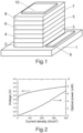
- Fig.1 presents a schematic axonometric view of the diode according to the invention.
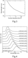
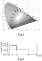
- Fig.2 presents the light-current-voltage (LIV) characteristics of an embodiment of a diode according to the invention, while Fig.3 presents the correlation between the emission wavelength and the density of the current powering said diode.
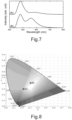
- Fig.4 presents standardised spectra of electroluminescence of the same diode for various current densities ranging from 0.5 A/cm 2 to 200 A/cm 2
- Fig.5 presents points corresponding to said spectra in a chromaticity diagram according to the CIE 1931 standard.
- Fig.6 presents an example time diagram of control of the power supply of the diode according to the invention.
- Fig.7 presents spectra of white light obtained by mixing blue and yellow light by the method according to the diagram in Fig.6
- Fig.8 presents points corresponding to said spectra in a chromaticity diagram according to the CIE 1931 standard.
- Fig.9 presents diagrams of the band structures of the active region, which reflect the scheme of operation of a diode according to the invention for four different voltages powering said diode.
- Fig.1 shows that the embodiment of a diode according to the invention contains a set of epitaxial layers, which is composed successively, counted from the crystalline substrate 1, of an n -type conductivity layer 2, an active region (layers from 3 through 6), an electron blocking layer 7 and a p -type conductivity layer 8.
- the aforementioned active region is composed of four successive layers: a lower n -type doped barrier layer 3, a lower n -type doped part 4 of the quantum well, an upper p -type doped part 5 of the quantum well, and an upper p -type doped barrier layer 6.
- Such a diode contains a first current terminal 9, connected electrically with the lower n -type conductivity layer 2, and a second current terminal 10, connected electrically with the p -type conductivity layer 8.
- This diode was fabricated in the process of nitrogen plasma assisted molecular beam epitaxy (PAMBE) growth in a Veeco GEN-20 reactor.
- the substrate 1 with the thickness of 350 ⁇ m, made of gallium nitride, was heated in a prechamber of said reactor at the temperature of 150°C for 90 minutes. The heating of the substrate 1 was continued for 30 minutes in a preparatory chamber at the temperature of 650°C. The heated substrate 1 was transferred to a growth chamber.
- the layer epitaxy was performed in metal-rich conditions. Nitrogen in the form of plasma excited by radio frequencies by a power supply unit was used for the growth, wherein the plasma parameters varied depending on the currently grown layer.
- GaN layers nitrogen flow was set at 2.2 cm 3 /min and the power supply unit's power was set at 250 W.
- said parameters were 10 cm 3 /min and 340 W, respectively.
- the growth of the GaN layers was performed at the temperature of 730°C, while of the InGaN layers - at the temperature of 650°C.
- n -type dopant materials such as gallium, indium and aluminium, and n -type dopant materials, that is, silicon and germanium, were evaporated from standard Knudsen cells, while as a source of p -type magnesium dopant a special structure of the Knudsen cell was used, which had an additional valve inside the cell, which valve allows a faster adjustment of the magnesium dopant atom flux size during the growth. The purity of the elements used for the epitaxy exceeded 99.999%. Firstly, on the substrate 1 a layer 2 ( n -type) with the thickness of 100 nm was fabricated of GaN, with the silicon doping level of 1 ⁇ 10 18 cm -3 .
- an active region (3, 4, 5, 6) was fabricated, which at the bottom contained a lower barrier layer 3 with the thickness of 60 nm, made of the silicon-doped In 0.02 Ga 0.98 N alloy with the doping level of 4 ⁇ 10 18 cm -3 .
- Another layer of said region was a lower part of the quantum well 4 with the thickness of 7.8 nm, made of the germanium-doped In 0.17 Ga 0.83 N alloy with the doping level of 6 ⁇ 10 19 cm -3 .
- the next layer of the active region was an upper part of the quantum well 5 with the thickness of 7.8 nm, made of the magnesium-doped In 0.17 Ga 0.83 N alloy with the doping level of 6 ⁇ 10 19 cm -3 .
- the last layer of the active region was an upper barrier layer 6 with the thickness of 60 nm, made of the magnesium-doped In 0.02 Ga 0.98 N alloy with the doping level of 4 ⁇ 10 18 cm -3 .
- an electron blocking layer 7 with the thickness of 20 nm, made of magnesium-doped GaN with the doping level of 2 ⁇ 10 19 cm -3 , was fabricated.
- a p -type conductivity layer 8 was fabricated, composed of a first sublayer with the thickness of 100 nm, made of magnesium-doped gallium nitride with the doping level of 1 ⁇ 10 18 cm -3 , of a second sublayer with the thickness of 40 nm, made of the magnesium-doped In 0.02 Ga 0.98 N alloy with the doping level of 6 ⁇ 10 19 cm -3 , and of a third sublayer with the thickness of 5 nm, made of the magnesium-doped In 0.17 Ga 0.83 N alloy with the doping level of 2 ⁇ 10 20 cm -3 .
- metallisation composed of a sequence of Ni/Au with the thickness of 2.5/7.5 nm was applied and subjected to the heating process in the nitrogen and oxygen atmosphere for one minute at the temperature of 500°C. Subsequently, said structure was subjected to photolithography and reactive ion etching to form mesas with the dimensions of 350 ⁇ 350 ⁇ m and 100 ⁇ 100 ⁇ m, which were etched 400 nm deep, that is, to the level of the n -type conductivity layer 2.
- Ni/Au/Pt metallisation with the thickness of 25/75/60 nm was applied in the form of grids with the dimensions of 340 ⁇ 340 ⁇ m on the mesas with the dimensions of 350 ⁇ 350 ⁇ m and in the form of solid squares with the dimensions of 90 ⁇ 90 ⁇ m on the mesas with the dimensions of 100 ⁇ 100 ⁇ m, composing the second (upper) current terminal 10.
- the metallisations were heated again in the nitrogen and oxygen atmosphere for ten minutes at the temperature of 500°C.
- metallisation of Ti/AI/Ni/ Au with the thickness of 30/60/40/75 nm, composing the first (lower) current terminal 9 was applied on the side of the mesas.
- the electrooptical properties of the fabricated structure were measured by the needle method, wherein a power supply unit and a voltage meter were interfaced with a spectrometer and an optical power meter.
- the optical power meter was placed at a constant height above the sample surface but it did not collect the whole light emitted from the sample to the outside, hence the optical powers presented in the chart ( Fig.2 ) are purely qualitative.
- the embodiment of a diode with the mesa size of 350 ⁇ 350 ⁇ m has current-voltage (I-V) characteristics in the forward direction that is typical of a LED, but the diode opening voltage is relatively low: circa 2.2 V.
- Optical power emitted from said diode increases approximately in a linear manner as a function of current density.
- Fig.3 presents a semi-log plot with the change in the wavelength of the light emitted from the embodiment of a diode as a function of current density. The spectrum maximum shifts towards the shorter waves within the range from 645 nm to 481 nm in line with the increase in the density of the current flowing through the diode within the range from 0.3 A/cm 2 to 400 A/cm 2 .
- Fig.4 presents standardised electroluminescence spectra for nine selected current densities, designated with letters from (a) through (i) in the drawing.
- Fig.5 the same spectra (for the same current densities as in Fig.4 ) are presented in the chromaticity diagram of the CIE1931 colour space.
- the colour of the light emitted from the diode according to the invention can be continuously changed within the whole visible spectrum, that is, from the red, to orange, yellow, green, cyan to blue, by changing the density of the current flowing through the diode, which is equivalent to a change in the voltage powering the diode.
- Fig.6 A scheme of such a power supply is presented in Fig.6 .
- the current (I) or voltage (V) powering the diode changes stepwise.
- a power supply level By selecting a power supply level, the wavelength of one of the peaks in the final spectrum is changed, and its intensity is adjusted by the duration.
- This way it is possible to set, for example, four power supply levels, with three responsible for emission of light of an appropriate primary colour: blue I 1 (V 1 ), green I 2 (V 2 ) and red I 3 (V 3 ), and the zero level lo(Vo), for which no emission occurs.
- the final lighting power can be reduced by prolonging the duration of the zero level.
- Fig.7 presents two spectra (A) and (B) of white light, obtained with the use of the power supply scheme described above, which uses two different power supply levels (V 1 and V 2 ) for the embodiment of a diode according to the invention with the dimensions of 100 ⁇ 100 ⁇ m.
- Fig.8 the same spectra as in Fig.7 are presented in the chromaticity diagram of the CIE 1931 colour space.
- Such a waveform of the power supply was achieved with the use of a programmable arbitrary power supply unit, Siglent SDG2042X.
- Fig.9 presents four band diagrams as a function of distance from crystalline substrate, prepared for four different voltages applied to the diode according to the invention, which illustrate the method of operation of such a diode.
- Diagram a) refers to the voltage of 2 V
- conduction and valence bands inside quantum wells are bent because of the strong doping of the individual parts of quantum wells.
- the energy difference between the energy levels of the wave functions for holes and electrons changes in line with the increase in the voltage powering the diode from 2.2 eV to 2.6 eV. This effect is responsible for the change in the colour of the emission from the diode.
- Diagrams c) and d) prepared for higher voltages that is, 3 V and 3.5 V, respectively, show that a quantum well is then virtually flat and resembles a case of an undoped well, wherein the energy difference between the energy levels of the wave functions for holes and electrons does not change and the electroluminescence wavelength is defined by the indium content in the quantum well.
Landscapes
- Led Devices (AREA)
- Physical Deposition Of Substances That Are Components Of Semiconductor Devices (AREA)
Abstract
Description
- The present invention relates to a wavelength tunable light emitting diode and a method of fabrication of such diode.
- Conventional light emitting diodes (LEDs) are built such that the diode's undoped active region, which contains one or more quantum wells, is located between p- and n-type doped layers. At present, commercially available light emitting diodes based on gallium nitride (GaN) and on alloys of gallium with aluminium (AIGaN) and indium (InGaN) emit light ranging from ultraviolet to green, depending on the composition of the alloy forming the quantum wells in the active region. Information about the structure of standard LEDs based on III group metal nitrides can be found, among others, in "Introduction to Nitride Semiconductor Blue Lasers and Light Emitting Diodes" by S. Nakamura and S. F. Chichibu [ISBN 9780748408368, CRC Press, 2000]. Light emission from a conventional LED is a single peak with the half-width of about a dozen nanometres. In the case of GaN-based diodes, the position of this peak as a function of current changes slightly, that is, by a few nanometres in the direction of the shorter wavelength and this effect is related to the screening of electric fields by the quantum-confined Stark effect (QCSE). Nevertheless, this effect is not strong enough to change the emission colour from red to blue in LEDs with a standard structure.
- Devices wherein the colour of the emitted light can be changed within a broad range of the visible light spectrum are most often sets of independently controlled LEDs with strictly defined emission wavelengths. The most basic combination is made by blue (~450 nm), green (~520 nm) and red (~650 nm) colour diodes. By independent control of the light emission power of each of the diodes it is possible to obtain light with any colour, including white light. The level of LED integration can occur at various stages of the engineering process. These can be large LEDs present in the RGB LED strips available on the market or micro-LED arrays. Methods of integration of single micro-LEDs for the purpose of production of multi-colour displays are disclosed in the review publication titled "Full-Color Realization of Micro-LED Displays" by Y. Wu et al. [Nanomaterials 2020, 10, 2482]. Such methods are described there as transfer and bonding of micro-LED chips made of group III metal nitrides and arsenides for dedicated drive substrates in various epitaxial processes, conversion of light from blue colour micro-LEDs to red and green colour with the use of luminophores or quantum dots or monolithic growth of multi-colour LEDs on the same substrate.
- Monolithic displays containing diodes with all three primary colours can be made only within the III nitrides, because the band gap of the indium gallium nitride (InGaN) alloy is the only one to cover the whole visible spectrum. The emission wavelength increases in line with the increase in the indium content in the InGaN alloy and in order to achieve the red light emission the indium content in the quantum well alloy should be circa 40%. Such a high indium content in planar structures is difficult to obtain due to high stresses of the InGaN layers and to the demanding conditions for epitaxy. Integration of indium in the micro-LED structure can be controlled at the nanostructure level, which is disclosed in the publication by Ra, Y.-H. et al. titled "Full-Color Single Nanowire Pixels for Projection Displays" [Nano Letters, 2016, 16(7), pp. 4608-4615]. The epitaxy of the InGaN/GaN heterostructure by the PAMBE method, described in said publication, was carried out on a GaN substrate covered with a layer made of titanium, wherein openings with various diameters were left. The epitaxial structure growth occurred only in the openings left in the titanium mask and this way InGaN quantum dots were grown inside nanowires (dot-in-nanowire). Moreover, during the epitaxy of InGaN quantum dots the indium content increased strongly in line with the decrease in the diameter of the nanowires, which resulted in a shift of the emission length in the direction of red colour. This way, by selecting appropriate diameters of the openings in the titanium mask, a multi-colour micro-LED array with four emission colours was made: blue, green, orange and red. But even in this solution a single subpixel structure was still responsible for emitting light with a single colour. It is a disadvantage of the solution wherein three subpixels have different colours that the colour of the light from a single pixel becomes homogeneous for the eye only when observed from an appropriately long distance. This is because when observed from a short distance the component colours of subpixels can be distinguished. In addition, a single maximum for the wavelength that is different from those corresponding to the emissions from single subpixels cannot be achieved in the electroluminescence spectrum. In order to eliminate said disadvantages, such light sources were sought the emission wavelength of which could be changed continuously by changing the power supply voltage or the density of the current flowing through the structure.
- Electrically tunable wavelength of emission from a single electroluminescent structure is disclosed in the publication by Y. J. Hong et al. titled "Visible-Color-Tunable Light-Emitting Diodes" [Adv. Mater. 2011, 23, 3284-3288]. These were LEDs made by the MOVPE method, built of a range of nanorods containing multiple InGaN/GaN quantum wells covered with a GaN:Mg layer. InGaN/GaN quantum wells can be distinguished in the structure of a single nanorod, which are located on the side walls, on the slants and on the top of the nanorods with various indium contents, being from 15% on the side walls to 60% on the top of the nanorods. By changing the power supply voltage, the emission wavelength was changed continuously from 690 nm (for 3 V) to 500 nm (for 10 V). This effect was explained by an appropriate model of electric field distribution in the nanorod structure. For the lowest power supply voltage, current with a low density flows preferably through InGaN wells with a high indium content on the top of the nanorods. In line with the increase in the power supply voltage, current with an increasingly higher density flows successively through the quantum wells on the slants and the side walls of the nanorods.
- The solution of a LED with an electrically tunable emission wavelength, disclosed in
US10418516B2 - In the aforementioned publications, electroluminescence from diodes based on III nitrides is approached in a traditional manner, wherein the emission wavelength is determined by the indium content in the InGaN alloy forming the quantum well, while there are no publications which would suggest the possibility to obtain an electroluminescent structure wherein the emission wavelength could be changed within a broad range of the visible spectrum, that is, within the wavelength range from 370 nm to 750 nm, from a single and the same quantum well with a relatively low indium content, being for example circa 17%.
- It is an object of the invention to obtain a light emitting diode with a flat structure, enabling light emission within the visible spectrum, that is, with the light wavelength ranging from 370 nm to 750 nm, wherein the emission colour is changed by changing the intensity of the current powering such a diode.
- This object is achieved by a diode according to the invention, which has an epitaxial layer structure built of nitrides of group III metals applied to a crystalline substrate. This structure is composed, counted from the crystalline substrate, of at least an n-type conductivity layer, a light emitting active region with one quantum well, and a p-type conductivity layer. The present invention consists in the active region that is composed, counted from the crystalline substrate, of a lower n-type doped barrier layer, a lower n-type doped part of the quantum well, an upper p-type doped part of the quantum well, and an upper p-type doped barrier layer. The width of each part of the quantum well ranges from 4 nm to 25 nm. The doping level of each part of the quantum well ranges from 1 × 1019 cm-3 to 2 × 1020 cm-3, while the doping level of the barrier layer is up to 25% of the doping level of the part of the quantum well that is adjacent to said barrier layer.
- In one of the variants of the diode according to the invention, each part of the quantum well is made of the InxGa1-xN indium gallium nitride alloy, each barrier layer is made of the InyGa1-yN indium gallium nitride alloy, wherein the indium content in said alloys is determined by the following correlation: 0 ≤ y < x ≤ 0.3.
- In another variant of the diode according to the invention, the width of the upper part of the quantum well is between 20% and 80% of the sum of widths of both parts of the quantum well.
- In still another variant of the diode according to the invention, between the upper barrier layer and the p-type conductivity layer is additionally an electron blocking layer, made of the AlxGa1-xN aluminium gallium nitride alloy wherein the aluminium content ranges from 0 to 0.2, wherein the doping level of said layer ranges from 5 × 1018 cm-3 to 5 × 1019 cm-3.
- The method according to the invention consists in fabricating an epitaxial layer structure on a crystalline substrate, with the structure's containing, counted from the crystalline substrate, at least an n-type conductivity layer, a light emitting active region with one quantum well and a p-type conductivity layer, of nitrides of group III metals in the process of nitrogen plasma assisted molecular beam epitaxy (PAMBE) growth. The invention is characterised in that an n-type conductivity layer, a four-layer active region and a p-type conductivity layer are successively fabricated on a crystalline substrate. While fabricating the active region, first its lower n-type doped barrier layer is fabricated. Subsequently, a lower n-type doped part of the quantum well is fabricated, after which an upper p-type doped part of the quantum well is fabricated. The fabrication of the active region is finished by applying an upper p-type doped barrier layer. While fabricating both parts of the quantum well, their width ranging from 4 nm to 25 nm and the doping level ranging from 1 × 1019 cm-3 to 2 × 1020 cm-3 are applied. While fabricating each barrier layer of the active region, the doping level of up to 25% of the doping level of the part of the quantum well that is adjacent to the barrier layer being fabricated is applied.
- In one of the variants of the method according to the invention, each part of the quantum well is made of the InxGa1-xN indium gallium nitride alloy, and each barrier layer is made of the InyGa1-yN indium gallium nitride alloy, by applying the indium content in said alloys that is determined by the following correlation: 0 ≤ y < x ≤ 0.3.
- In another variant of the method according to the invention, an upper part of the quantum well is fabricated with the width being between 20% and 80% of the sum of widths of both parts of the quantum well.
- In another variant of the method according to the invention, an electron blocking layer is applied additionally between the upper barrier layer and the p-type conductivity layer. For fabrication of said layer, the AlxGa1-xN aluminium gallium nitride alloy is used, wherein the aluminium content ranges from 0 to 0.2 and the doping level ranges from 5 × 1018 cm-3 to 5 × 1019 cm-3.
- In still another variant of the method according to the invention, the epitaxial growth of the layer structure is performed in metal-rich conditions. Epitaxial layers of said structure are applied at the temperature ranging from 600°C to 800°C, while nitrogen for epitaxial growth of the layer structure is supplied in the form of plasma excited by a power supply unit generating a power between 100 and 600 W, with the nitrogen flow between 1 and 15 cm3 per minute.
- The invention breaks the conviction prevailing commonly among specialists that in order to obtain red electroluminescence of a LED fabricated using the technology of nitrides of group III metals, the indium content in the quantum well must be increased to circa 35%. It has turned out unexpectedly that it is possible to obtain lighting from a single quantum well placed in the layer structure of a LED with a much higher wavelength than could be expected from the energy of the band gap of the alloy forming the quantum well, and that the wavelength of emission from such a quantum well can be changed continuously by changing the density of the current flowing through the LED structure. This is possible through an appropriate engineering of the doping of the active region containing one quantum well with the width between 8 nm and 50 nm.
- The present invention is reflected in the drawing, with
Fig.1 presenting a schematic axonometric view of the diode according to the invention.Fig.2 presents the light-current-voltage (LIV) characteristics of an embodiment of a diode according to the invention, whileFig.3 presents the correlation between the emission wavelength and the density of the current powering said diode.Fig.4 presents standardised spectra of electroluminescence of the same diode for various current densities ranging from 0.5 A/cm2 to 200 A/cm2, whileFig.5 presents points corresponding to said spectra in a chromaticity diagram according to the CIE 1931 standard.Fig.6 presents an example time diagram of control of the power supply of the diode according to the invention.Fig.7 presents spectra of white light obtained by mixing blue and yellow light by the method according to the diagram inFig.6 , whileFig.8 presents points corresponding to said spectra in a chromaticity diagram according to the CIE 1931 standard.Fig.9 presents diagrams of the band structures of the active region, which reflect the scheme of operation of a diode according to the invention for four different voltages powering said diode. - The present invention is presented in more detail in the embodiment described below.
Fig.1 shows that the embodiment of a diode according to the invention contains a set of epitaxial layers, which is composed successively, counted from thecrystalline substrate 1, of an n-type conductivity layer 2, an active region (layers from 3 through 6), anelectron blocking layer 7 and a p-type conductivity layer 8. The aforementioned active region is composed of four successive layers: a lower n-type dopedbarrier layer 3, a lower n-type dopedpart 4 of the quantum well, an upper p-type dopedpart 5 of the quantum well, and an upper p-type dopedbarrier layer 6. Such a diode contains a firstcurrent terminal 9, connected electrically with the lower n-type conductivity layer 2, and a secondcurrent terminal 10, connected electrically with the p-type conductivity layer 8. - This diode was fabricated in the process of nitrogen plasma assisted molecular beam epitaxy (PAMBE) growth in a Veeco GEN-20 reactor. The
substrate 1 with the thickness of 350 µm, made of gallium nitride, was heated in a prechamber of said reactor at the temperature of 150°C for 90 minutes. The heating of thesubstrate 1 was continued for 30 minutes in a preparatory chamber at the temperature of 650°C. Theheated substrate 1 was transferred to a growth chamber. The layer epitaxy was performed in metal-rich conditions. Nitrogen in the form of plasma excited by radio frequencies by a power supply unit was used for the growth, wherein the plasma parameters varied depending on the currently grown layer. For the GaN layers, nitrogen flow was set at 2.2 cm3/min and the power supply unit's power was set at 250 W. For the InGaN layers, said parameters were 10 cm3/min and 340 W, respectively. The growth of the GaN layers was performed at the temperature of 730°C, while of the InGaN layers - at the temperature of 650°C. Metals forming the alloys, such as gallium, indium and aluminium, and n-type dopant materials, that is, silicon and germanium, were evaporated from standard Knudsen cells, while as a source of p-type magnesium dopant a special structure of the Knudsen cell was used, which had an additional valve inside the cell, which valve allows a faster adjustment of the magnesium dopant atom flux size during the growth. The purity of the elements used for the epitaxy exceeded 99.999%. Firstly, on the substrate 1 a layer 2 (n-type) with the thickness of 100 nm was fabricated of GaN, with the silicon doping level of 1 × 1018 cm-3. Subsequently, an active region (3, 4, 5, 6) was fabricated, which at the bottom contained alower barrier layer 3 with the thickness of 60 nm, made of the silicon-doped In0.02Ga0.98N alloy with the doping level of 4 × 1018 cm-3. Another layer of said region was a lower part of the quantum well 4 with the thickness of 7.8 nm, made of the germanium-doped In0.17Ga0.83N alloy with the doping level of 6 × 1019 cm-3. The next layer of the active region was an upper part of the quantum well 5 with the thickness of 7.8 nm, made of the magnesium-doped In0.17Ga0.83N alloy with the doping level of 6 × 1019 cm-3. The last layer of the active region was anupper barrier layer 6 with the thickness of 60 nm, made of the magnesium-doped In0.02Ga0.98N alloy with the doping level of 4 × 1018 cm-3. On the finished active region, anelectron blocking layer 7 with the thickness of 20 nm, made of magnesium-doped GaN with the doping level of 2 × 1019 cm-3, was fabricated. As the last one, a p-type conductivity layer 8 was fabricated, composed of a first sublayer with the thickness of 100 nm, made of magnesium-doped gallium nitride with the doping level of 1 × 1018 cm-3, of a second sublayer with the thickness of 40 nm, made of the magnesium-doped In0.02Ga0.98N alloy with the doping level of 6 × 1019 cm-3, and of a third sublayer with the thickness of 5 nm, made of the magnesium-doped In0.17Ga0.83N alloy with the doping level of 2 × 1020 cm-3. On the top of the epitaxial structure fabricated by the aforementioned method, metallisation composed of a sequence of Ni/Au with the thickness of 2.5/7.5 nm was applied and subjected to the heating process in the nitrogen and oxygen atmosphere for one minute at the temperature of 500°C. Subsequently, said structure was subjected to photolithography and reactive ion etching to form mesas with the dimensions of 350 × 350 µm and 100 × 100 µm, which were etched 400 nm deep, that is, to the level of the n-type conductivity layer 2. On the top of the fabricated mesas, next Ni/Au/Pt metallisation with the thickness of 25/75/60 nm was applied in the form of grids with the dimensions of 340 × 340 µm on the mesas with the dimensions of 350 × 350 µm and in the form of solid squares with the dimensions of 90 × 90 µm on the mesas with the dimensions of 100 × 100 µm, composing the second (upper)current terminal 10. Subsequently, the metallisations were heated again in the nitrogen and oxygen atmosphere for ten minutes at the temperature of 500°C. At the last stage, metallisation of Ti/AI/Ni/ Au with the thickness of 30/60/40/75 nm, composing the first (lower)current terminal 9, was applied on the side of the mesas. - The electrooptical properties of the fabricated structure were measured by the needle method, wherein a power supply unit and a voltage meter were interfaced with a spectrometer and an optical power meter. The optical power meter was placed at a constant height above the sample surface but it did not collect the whole light emitted from the sample to the outside, hence the optical powers presented in the chart (
Fig.2 ) are purely qualitative. As reflected inFig.2 , the embodiment of a diode with the mesa size of 350 × 350 µm has current-voltage (I-V) characteristics in the forward direction that is typical of a LED, but the diode opening voltage is relatively low: circa 2.2 V. Optical power emitted from said diode increases approximately in a linear manner as a function of current density.Fig.3 presents a semi-log plot with the change in the wavelength of the light emitted from the embodiment of a diode as a function of current density. The spectrum maximum shifts towards the shorter waves within the range from 645 nm to 481 nm in line with the increase in the density of the current flowing through the diode within the range from 0.3 A/cm2 to 400 A/cm2.Fig.4 presents standardised electroluminescence spectra for nine selected current densities, designated with letters from (a) through (i) in the drawing. InFig.5 , the same spectra (for the same current densities as inFig.4 ) are presented in the chromaticity diagram of the CIE1931 colour space. As reflected inFig.2 through Fig.5 , the colour of the light emitted from the diode according to the invention can be continuously changed within the whole visible spectrum, that is, from the red, to orange, yellow, green, cyan to blue, by changing the density of the current flowing through the diode, which is equivalent to a change in the voltage powering the diode. - Through appropriate power supply of the diode according to the invention, it is possible to control its power and mix the colours emitted by said diode in order to form white light and other colours in the CIE 1931 space.
- A scheme of such a power supply is presented in
Fig.6 . The current (I) or voltage (V) powering the diode changes stepwise. By selecting a power supply level, the wavelength of one of the peaks in the final spectrum is changed, and its intensity is adjusted by the duration. This way it is possible to set, for example, four power supply levels, with three responsible for emission of light of an appropriate primary colour: blue I1(V1), green I2(V2) and red I3(V3), and the zero level lo(Vo), for which no emission occurs. The final lighting power can be reduced by prolonging the duration of the zero level. -
Fig.7 presents two spectra (A) and (B) of white light, obtained with the use of the power supply scheme described above, which uses two different power supply levels (V1 and V2) for the embodiment of a diode according to the invention with the dimensions of 100 × 100 µm. InFig.8 , the same spectra as inFig.7 are presented in the chromaticity diagram of the CIE 1931 colour space. Such a waveform of the power supply was achieved with the use of a programmable arbitrary power supply unit, Siglent SDG2042X. In the case of the spectrum designated with (A), cold white light was achieved when the diode was powered with voltages V1 = 3.5 V and V2 = 2.1 V, while the time of powering with voltage V2 (for example, from t1 to t2 inFig.6 ) was 2046 times longer than the time of its powering with voltage V1 (for example, from to to t1 inFig.6 ). In the case of the spectrum designated with (B), in turn, warm white light was achieved when the diode was powered with voltages V1 = 3.7 V and V2 = 2.22 V, while the time of powering with voltage V2 was 2046 times longer than the time of its powering with voltage V1. In both cases, voltage levels changed cyclically with the frequency of 1 kHz, which means that the aggregate duration of both power supply voltages in one cycle was 0.001 s. -
Fig.9 presents four band diagrams as a function of distance from crystalline substrate, prepared for four different voltages applied to the diode according to the invention, which illustrate the method of operation of such a diode. Diagram a) refers to the voltage of 2 V, while diagram b) - to the voltage of 2.5 V. As shown in the aforementioned diagrams, conduction and valence bands inside quantum wells are bent because of the strong doping of the individual parts of quantum wells. In this regard, the energy difference between the energy levels of the wave functions for holes and electrons changes in line with the increase in the voltage powering the diode from 2.2 eV to 2.6 eV. This effect is responsible for the change in the colour of the emission from the diode. Diagrams c) and d) prepared for higher voltages, that is, 3 V and 3.5 V, respectively, show that a quantum well is then virtually flat and resembles a case of an undoped well, wherein the energy difference between the energy levels of the wave functions for holes and electrons does not change and the electroluminescence wavelength is defined by the indium content in the quantum well.
Claims (9)
- A light emitting diode with a variable light emission colour, having an epitaxial layer structure built of nitrides of group III metals applied to a crystalline substrate, which structure is composed, counted from the crystalline substrate, of at least an n-type conductivity layer, a light emitting active region with one quantum well, and a p-type conductivity layer, characterised in that the active region (3, 4, 5, 6) is composed, counted from the crystalline substrate (1), of a lower n-type doped barrier layer (3), a lower n-type doped part (4) of the quantum well, an upper p-type doped part (5) of the quantum well, and an upper p-type doped barrier layer (6), wherein the width of each part (4, 5) of the quantum well ranges from 4 nm to 25 nm, the doping level of each part (4, 5) of the quantum well ranges from 1 × 1019 cm-3 to 2 × 1020 cm-3, while the doping level of the barrier layer (3, 6) is up to 25% of the doping level of the part of the quantum well (4, 5) that is adjacent to said barrier layer (3, 6).
- The diode according to claim 1, characterised in that each part (4, 5) of the quantum well is made of the InxGa1-xN indium gallium nitride alloy, each barrier layer (3, 6) is made of the InyGa1-yN indium gallium nitride alloy, wherein the indium content in said alloys is determined by the following correlation: 0 ≤ y < x ≤ 0.3.
- The diode according to claim 1 or 2, characterised in that the width of the upper part (5) of the quantum well is between 20% and 80% of the sum of widths of both parts (4, 5) of the quantum well.
- The diode according to claim 1 or 2 or 3, characterised in that between the upper barrier layer (6) and the p-type conductivity layer (8) is additionally an electron blocking layer (7), made of the AlxGa1-xN aluminium gallium nitride alloy wherein the aluminium content ranges from 0 to 0.2, wherein the doping level of said layer (7) ranges from 5 × 1018 cm-3 to 5 × 1019 cm-3.
- A method of fabrication of a light emitting diode with a variable light emission colour, consisting in fabricating an epitaxial layer structure on a crystalline substrate, with the structure's containing, counted from the crystalline substrate, at least an n-type conductivity layer, a light emitting active region with one quantum well and a p-type conductivity layer, of nitrides of group III metals in the process of nitrogen plasma assisted molecular beam epitaxy (PAMBE) growth, characterised in that an n-type conductivity layer (2), a four-layer active region (3, 4, 5, 6) and a p-type conductivity layer (8) are successively fabricated on a crystalline substrate (1), wherein, while fabricating the active region (3, 4, 5, 6), first its lower n-type doped barrier layer (3) is fabricated, subsequently, a lower n-type doped part (4) of the quantum well is fabricated, after which an upper p-type doped part (5) of the quantum well is fabricated, and finally an upper p-type doped barrier layer (6) is fabricated, wherein, while fabricating each part (4, 5) of the quantum well, their width ranging from 4 nm to 25 nm and the doping level ranging from 1 × 1019 cm-3 to 2 × 1020 cm-3 are applied, and while fabricating each barrier layer (3, 6) of the active region, the doping level of up to 25% of the doping level of the part (4, 5) of the quantum well that is adjacent to the barrier layer (3, 6) being fabricated is applied.
- The method according to claim 5, characterised in that each part (4, 5) of the quantum well is made of the InxGa1-xN indium gallium nitride alloy, and each barrier layer (3, 6) is made of the InyGa1-yN indium gallium nitride alloy, by applying the indium content in said alloys that is determined by the following correlation: 0 ≤ y < x ≤ 0.3.
- The method according to claim 5 or 6, characterised in that in the process of growth of the active region (3, 4, 5, 6) an upper part (5) of the quantum well is fabricated with the width being between 20% and 80% of the sum of widths of both parts (4, 5) of the quantum well.
- The method according to claim 5 or 6 or 7, characterised in that an electron blocking layer (7) is applied additionally between the upper barrier layer (6) and the p-type conductivity layer (8), and for fabrication of said layer, the AlxGa1-xN aluminium gallium nitride alloy is used, wherein the aluminium content ranges from 0 to 0.2 and the doping level of said layer (7) ranges from 5 × 1018 cm-3 to 5 × 1019 cm-3.
- The method according to claim 5 or 6 or 7 or 8, characterised in that the epitaxial growth of the layer structure is performed in metal-rich conditions, the epitaxial layers (2 through 8) are applied at the temperature ranging from 600°C to 800°C, while nitrogen for epitaxial growth of the layer structure is supplied in the form of plasma excited by a power supply unit generating a power between 100 and 600 W, with the nitrogen flow between 1 and 15 cm3 per minute.
Applications Claiming Priority (1)
| Application Number | Priority Date | Filing Date | Title |
|---|---|---|---|
| PL440375A PL440375A1 (en) | 2022-02-12 | 2022-02-12 | Light-emitting diode with variable emission color and method of producing such a diode |
Publications (3)
| Publication Number | Publication Date |
|---|---|
| EP4228012A1 true EP4228012A1 (en) | 2023-08-16 |
| EP4228012B1 EP4228012B1 (en) | 2024-09-25 |
| EP4228012C0 EP4228012C0 (en) | 2024-09-25 |
Family
ID=83006096
Family Applications (1)
| Application Number | Title | Priority Date | Filing Date |
|---|---|---|---|
| EP22461577.3A Active EP4228012B1 (en) | 2022-02-12 | 2022-06-23 | Wavelength tunable light emitting diode and method of making the same |
Country Status (2)
| Country | Link |
|---|---|
| EP (1) | EP4228012B1 (en) |
| PL (2) | PL440375A1 (en) |
Cited By (1)
| Publication number | Priority date | Publication date | Assignee | Title |
|---|---|---|---|---|
| CN117457821A (en) * | 2023-12-21 | 2024-01-26 | 江西兆驰半导体有限公司 | Micro-LED epitaxial wafer and preparation method thereof, Micro-LED |
Citations (3)
| Publication number | Priority date | Publication date | Assignee | Title |
|---|---|---|---|---|
| JP2002237619A (en) * | 2001-02-13 | 2002-08-23 | Japan Science & Technology Corp | Light emission color control method for light emitting diode |
| WO2008030183A1 (en) * | 2006-09-08 | 2008-03-13 | Agency For Science, Technology And Research | Tunable wavelength light emitting diode |
| US10418516B2 (en) | 2015-06-05 | 2019-09-17 | Ostendo Technologies, Inc. | White light emitting structures with controllable emission color temperature |
-
2022
- 2022-02-12 PL PL440375A patent/PL440375A1/en unknown
- 2022-06-23 EP EP22461577.3A patent/EP4228012B1/en active Active
- 2022-06-23 PL PL22461577.3T patent/PL4228012T3/en unknown
Patent Citations (3)
| Publication number | Priority date | Publication date | Assignee | Title |
|---|---|---|---|---|
| JP2002237619A (en) * | 2001-02-13 | 2002-08-23 | Japan Science & Technology Corp | Light emission color control method for light emitting diode |
| WO2008030183A1 (en) * | 2006-09-08 | 2008-03-13 | Agency For Science, Technology And Research | Tunable wavelength light emitting diode |
| US10418516B2 (en) | 2015-06-05 | 2019-09-17 | Ostendo Technologies, Inc. | White light emitting structures with controllable emission color temperature |
Non-Patent Citations (5)
| Title |
|---|
| LEE KWANJAE ET AL: "Flower-like light distribution inside InGaN-based light-emitting diodes operated in spectral range from violet to red", 2017 75TH ANNUAL DEVICE RESEARCH CONFERENCE (DRC), IEEE, 25 June 2017 (2017-06-25), pages 1 - 2, XP033135341, DOI: 10.1109/DRC.2017.7999457 * |
| RA, Y.-H.: "Full-Color Single Nanowire Pixels for Projection Displays", NANO LETTERS, vol. 16, no. 7, 2016, pages 4608 - 4615, XP055668994, DOI: 10.1021/acs.nanolett.6b01929 |
| S. NAKAMURAS. F. CHICHIBU: "Introduction to Nitride Semiconductor Blue Lasers and Light Emitting Diodes", 2000, CRC PRESS |
| Y. J. HONG ET AL.: "Visible-Color-Tunable Light-Emitting Diodes", ADV. MATER., vol. 23, 2011, pages 3284 - 3288, XP055057307, DOI: 10.1002/adma.201100806 |
| Y. WU ET AL.: "Full-Color Realization of Micro-LED Displays", NANOMATERIALS, vol. 10, 2020, pages 2482 |
Cited By (2)
| Publication number | Priority date | Publication date | Assignee | Title |
|---|---|---|---|---|
| CN117457821A (en) * | 2023-12-21 | 2024-01-26 | 江西兆驰半导体有限公司 | Micro-LED epitaxial wafer and preparation method thereof, Micro-LED |
| CN117457821B (en) * | 2023-12-21 | 2024-03-08 | 江西兆驰半导体有限公司 | Micro-LED epitaxial wafer and preparation method thereof, Micro-LED |
Also Published As
| Publication number | Publication date |
|---|---|
| EP4228012B1 (en) | 2024-09-25 |
| PL440375A1 (en) | 2023-08-14 |
| EP4228012C0 (en) | 2024-09-25 |
| PL4228012T3 (en) | 2025-01-27 |
Similar Documents
| Publication | Publication Date | Title |
|---|---|---|
| EP2254164B1 (en) | Compound semiconductor light-emitting element and illumination device using the same, and method for manufacturing compound semiconductor light-emitting element | |
| CN107851968B (en) | Light emitting structure with selective carrier injection into multiple active layers | |
| US6329676B1 (en) | Flat panel solid state light source | |
| US8022388B2 (en) | Broadband light emitting device lamps for providing white light output | |
| EP0732754B1 (en) | Light-emitting semiconductor device using group III nitride compound | |
| CN106165125B (en) | Light emitting diode and preparation method thereof | |
| EP2200100A1 (en) | Iii nitride semiconductor light emitting element | |
| US20050082544A1 (en) | Nitride semiconductor device, and its fabrication process | |
| KR101611412B1 (en) | Light emitting device | |
| KR101460387B1 (en) | Lightemitting structure | |
| JP2003520453A (en) | Chirped multi-well active area LED | |
| Lu et al. | Phosphor-free monolithic white-light LED | |
| EP4228012B1 (en) | Wavelength tunable light emitting diode and method of making the same | |
| CN114078989B (en) | Full-color light-emitting device | |
| EP4340050A1 (en) | Multi-band light emitting diode | |
| KR20080068244A (en) | Light Emitting Diodes Using Surface Plasmons | |
| US20260052802A1 (en) | Growth engineering of monolithic color-tunable light emitting diodes and methods thereof | |
| US20260052803A1 (en) | Growth engineering of monolithic and at least red emitting color-tunable light emitting diodes and methods thereof | |
| CN102709418A (en) | Spectrum adjustable zinc oxide (ZnO)/gallium nitride (GaN) based white light emitting device structure | |
| KR20090062501A (en) | Nitride semiconductor devices | |
| Dussaigne et al. | Monolithic white light emitting diodes with a broad emission spectrum | |
| HK40075839A (en) | Light emitting structures with selective carrier injection into multiple active layers | |
| JP2005353651A (en) | Semiconductor light emitting device and manufacturing method thereof | |
| CN120584409A (en) | Semiconductor device monolithic array, template wafer, method for manufacturing template wafer, method for manufacturing semiconductor device array | |
| US20010007361A1 (en) | Semiconductor light emitting device with high yield and low power consumption |
Legal Events
| Date | Code | Title | Description |
|---|---|---|---|
| STAA | Information on the status of an ep patent application or granted ep patent |
Free format text: STATUS: UNKNOWN |
|
| PUAI | Public reference made under article 153(3) epc to a published international application that has entered the european phase |
Free format text: ORIGINAL CODE: 0009012 |
|
| STAA | Information on the status of an ep patent application or granted ep patent |
Free format text: STATUS: THE APPLICATION HAS BEEN PUBLISHED |
|
| AK | Designated contracting states |
Kind code of ref document: A1 Designated state(s): AL AT BE BG CH CY CZ DE DK EE ES FI FR GB GR HR HU IE IS IT LI LT LU LV MC MK MT NL NO PL PT RO RS SE SI SK SM TR |
|
| RIN1 | Information on inventor provided before grant (corrected) |
Inventor name: SKIERBISZEWSKI, CZESLAW Inventor name: WOLNY, PAWEL Inventor name: HAJDEL, MATEUSZ Inventor name: MUZIOL, GRZEGORZ Inventor name: NOWAKOWSKI-SZKUDLAREK, KRZESIMIR Inventor name: CHLIPALA, MIKOLAJ Inventor name: TURSKI, HENRYK Inventor name: ZAK, MIKOLAJ |
|
| STAA | Information on the status of an ep patent application or granted ep patent |
Free format text: STATUS: REQUEST FOR EXAMINATION WAS MADE |
|
| 17P | Request for examination filed |
Effective date: 20231205 |
|
| RBV | Designated contracting states (corrected) |
Designated state(s): AL AT BE BG CH CY CZ DE DK EE ES FI FR GB GR HR HU IE IS IT LI LT LU LV MC MK MT NL NO PL PT RO RS SE SI SK SM TR |
|
| GRAP | Despatch of communication of intention to grant a patent |
Free format text: ORIGINAL CODE: EPIDOSNIGR1 |
|
| STAA | Information on the status of an ep patent application or granted ep patent |
Free format text: STATUS: GRANT OF PATENT IS INTENDED |
|
| RIC1 | Information provided on ipc code assigned before grant |
Ipc: H01L 33/14 20100101ALN20240530BHEP Ipc: H01L 33/32 20100101ALI20240530BHEP Ipc: H01L 33/06 20100101ALI20240530BHEP Ipc: H01L 33/02 20100101ALI20240530BHEP Ipc: H01L 33/00 20100101AFI20240530BHEP |
|
| INTG | Intention to grant announced |
Effective date: 20240620 |
|
| GRAS | Grant fee paid |
Free format text: ORIGINAL CODE: EPIDOSNIGR3 |
|
| GRAA | (expected) grant |
Free format text: ORIGINAL CODE: 0009210 |
|
| STAA | Information on the status of an ep patent application or granted ep patent |
Free format text: STATUS: THE PATENT HAS BEEN GRANTED |
|
| AK | Designated contracting states |
Kind code of ref document: B1 Designated state(s): AL AT BE BG CH CY CZ DE DK EE ES FI FR GB GR HR HU IE IS IT LI LT LU LV MC MK MT NL NO PL PT RO RS SE SI SK SM TR |
|
| REG | Reference to a national code |
Ref country code: GB Ref legal event code: FG4D |
|
| REG | Reference to a national code |
Ref country code: CH Ref legal event code: EP |
|
| REG | Reference to a national code |
Ref country code: DE Ref legal event code: R096 Ref document number: 602022006392 Country of ref document: DE |
|
| REG | Reference to a national code |
Ref country code: IE Ref legal event code: FG4D |
|
| U01 | Request for unitary effect filed |
Effective date: 20241015 |
|
| U07 | Unitary effect registered |
Designated state(s): AT BE BG DE DK EE FI FR IT LT LU LV MT NL PT RO SE SI Effective date: 20241031 |
|
| PG25 | Lapsed in a contracting state [announced via postgrant information from national office to epo] |
Ref country code: NO Free format text: LAPSE BECAUSE OF FAILURE TO SUBMIT A TRANSLATION OF THE DESCRIPTION OR TO PAY THE FEE WITHIN THE PRESCRIBED TIME-LIMIT Effective date: 20241225 |
|
| PG25 | Lapsed in a contracting state [announced via postgrant information from national office to epo] |
Ref country code: GR Free format text: LAPSE BECAUSE OF FAILURE TO SUBMIT A TRANSLATION OF THE DESCRIPTION OR TO PAY THE FEE WITHIN THE PRESCRIBED TIME-LIMIT Effective date: 20241226 |
|
| PG25 | Lapsed in a contracting state [announced via postgrant information from national office to epo] |
Ref country code: RS Free format text: LAPSE BECAUSE OF FAILURE TO SUBMIT A TRANSLATION OF THE DESCRIPTION OR TO PAY THE FEE WITHIN THE PRESCRIBED TIME-LIMIT Effective date: 20241225 |
|
| PG25 | Lapsed in a contracting state [announced via postgrant information from national office to epo] |
Ref country code: RS Free format text: LAPSE BECAUSE OF FAILURE TO SUBMIT A TRANSLATION OF THE DESCRIPTION OR TO PAY THE FEE WITHIN THE PRESCRIBED TIME-LIMIT Effective date: 20241225 Ref country code: NO Free format text: LAPSE BECAUSE OF FAILURE TO SUBMIT A TRANSLATION OF THE DESCRIPTION OR TO PAY THE FEE WITHIN THE PRESCRIBED TIME-LIMIT Effective date: 20241225 Ref country code: GR Free format text: LAPSE BECAUSE OF FAILURE TO SUBMIT A TRANSLATION OF THE DESCRIPTION OR TO PAY THE FEE WITHIN THE PRESCRIBED TIME-LIMIT Effective date: 20241226 |
|
| PG25 | Lapsed in a contracting state [announced via postgrant information from national office to epo] |
Ref country code: IS Free format text: LAPSE BECAUSE OF FAILURE TO SUBMIT A TRANSLATION OF THE DESCRIPTION OR TO PAY THE FEE WITHIN THE PRESCRIBED TIME-LIMIT Effective date: 20250125 |
|
| PG25 | Lapsed in a contracting state [announced via postgrant information from national office to epo] |
Ref country code: SM Free format text: LAPSE BECAUSE OF FAILURE TO SUBMIT A TRANSLATION OF THE DESCRIPTION OR TO PAY THE FEE WITHIN THE PRESCRIBED TIME-LIMIT Effective date: 20240925 |
|
| PG25 | Lapsed in a contracting state [announced via postgrant information from national office to epo] |
Ref country code: ES Free format text: LAPSE BECAUSE OF FAILURE TO SUBMIT A TRANSLATION OF THE DESCRIPTION OR TO PAY THE FEE WITHIN THE PRESCRIBED TIME-LIMIT Effective date: 20240925 |
|
| PG25 | Lapsed in a contracting state [announced via postgrant information from national office to epo] |
Ref country code: CZ Free format text: LAPSE BECAUSE OF FAILURE TO SUBMIT A TRANSLATION OF THE DESCRIPTION OR TO PAY THE FEE WITHIN THE PRESCRIBED TIME-LIMIT Effective date: 20240925 |
|
| PG25 | Lapsed in a contracting state [announced via postgrant information from national office to epo] |
Ref country code: SK Free format text: LAPSE BECAUSE OF FAILURE TO SUBMIT A TRANSLATION OF THE DESCRIPTION OR TO PAY THE FEE WITHIN THE PRESCRIBED TIME-LIMIT Effective date: 20240925 |
|
| PGFP | Annual fee paid to national office [announced via postgrant information from national office to epo] |
Ref country code: PL Payment date: 20250617 Year of fee payment: 4 |
|
| U20 | Renewal fee for the european patent with unitary effect paid |
Year of fee payment: 4 Effective date: 20250618 |
|
| PLBE | No opposition filed within time limit |
Free format text: ORIGINAL CODE: 0009261 |
|
| STAA | Information on the status of an ep patent application or granted ep patent |
Free format text: STATUS: NO OPPOSITION FILED WITHIN TIME LIMIT |
|
| 26N | No opposition filed |
Effective date: 20250626 |
|
| PG25 | Lapsed in a contracting state [announced via postgrant information from national office to epo] |
Ref country code: HR Free format text: LAPSE BECAUSE OF FAILURE TO SUBMIT A TRANSLATION OF THE DESCRIPTION OR TO PAY THE FEE WITHIN THE PRESCRIBED TIME-LIMIT Effective date: 20240925 |
|
| REG | Reference to a national code |
Ref country code: CH Ref legal event code: H13 Free format text: ST27 STATUS EVENT CODE: U-0-0-H10-H13 (AS PROVIDED BY THE NATIONAL OFFICE) Effective date: 20260127 |
|
| PG25 | Lapsed in a contracting state [announced via postgrant information from national office to epo] |
Ref country code: MC Free format text: LAPSE BECAUSE OF FAILURE TO SUBMIT A TRANSLATION OF THE DESCRIPTION OR TO PAY THE FEE WITHIN THE PRESCRIBED TIME-LIMIT Effective date: 20240925 |
|
| PG25 | Lapsed in a contracting state [announced via postgrant information from national office to epo] |
Ref country code: IE Free format text: LAPSE BECAUSE OF NON-PAYMENT OF DUE FEES Effective date: 20250623 |
|
| PG25 | Lapsed in a contracting state [announced via postgrant information from national office to epo] |
Ref country code: CH Free format text: LAPSE BECAUSE OF NON-PAYMENT OF DUE FEES Effective date: 20250630 |