EP4227995A1 - Power electronics module and method for its manufacturing - Google Patents
Power electronics module and method for its manufacturing Download PDFInfo
- Publication number
- EP4227995A1 EP4227995A1 EP22155917.2A EP22155917A EP4227995A1 EP 4227995 A1 EP4227995 A1 EP 4227995A1 EP 22155917 A EP22155917 A EP 22155917A EP 4227995 A1 EP4227995 A1 EP 4227995A1
- Authority
- EP
- European Patent Office
- Prior art keywords
- electronic devices
- power electronic
- layer
- group
- solder
- Prior art date
- Legal status (The legal status is an assumption and is not a legal conclusion. Google has not performed a legal analysis and makes no representation as to the accuracy of the status listed.)
- Granted
Links
Images




Classifications
-
- H—ELECTRICITY
- H10—SEMICONDUCTOR DEVICES; ELECTRIC SOLID-STATE DEVICES NOT OTHERWISE PROVIDED FOR
- H10W—GENERIC PACKAGES, INTERCONNECTIONS, CONNECTORS OR OTHER CONSTRUCTIONAL DETAILS OF DEVICES COVERED BY CLASS H10
- H10W90/00—Package configurations
-
- H—ELECTRICITY
- H10—SEMICONDUCTOR DEVICES; ELECTRIC SOLID-STATE DEVICES NOT OTHERWISE PROVIDED FOR
- H10W—GENERIC PACKAGES, INTERCONNECTIONS, CONNECTORS OR OTHER CONSTRUCTIONAL DETAILS OF DEVICES COVERED BY CLASS H10
- H10W72/00—Interconnections or connectors in packages
- H10W72/01—Manufacture or treatment
- H10W72/013—Manufacture or treatment of die-attach connectors
- H10W72/01321—Manufacture or treatment of die-attach connectors using local deposition
- H10W72/01323—Manufacture or treatment of die-attach connectors using local deposition in liquid form, e.g. by dispensing droplets or by screen printing
-
- H—ELECTRICITY
- H10—SEMICONDUCTOR DEVICES; ELECTRIC SOLID-STATE DEVICES NOT OTHERWISE PROVIDED FOR
- H10W—GENERIC PACKAGES, INTERCONNECTIONS, CONNECTORS OR OTHER CONSTRUCTIONAL DETAILS OF DEVICES COVERED BY CLASS H10
- H10W72/00—Interconnections or connectors in packages
- H10W72/071—Connecting or disconnecting
- H10W72/0711—Apparatus therefor
- H10W72/07141—Means for applying energy, e.g. ovens or lasers
-
- H—ELECTRICITY
- H10—SEMICONDUCTOR DEVICES; ELECTRIC SOLID-STATE DEVICES NOT OTHERWISE PROVIDED FOR
- H10W—GENERIC PACKAGES, INTERCONNECTIONS, CONNECTORS OR OTHER CONSTRUCTIONAL DETAILS OF DEVICES COVERED BY CLASS H10
- H10W72/00—Interconnections or connectors in packages
- H10W72/071—Connecting or disconnecting
- H10W72/073—Connecting or disconnecting of die-attach connectors
-
- H—ELECTRICITY
- H10—SEMICONDUCTOR DEVICES; ELECTRIC SOLID-STATE DEVICES NOT OTHERWISE PROVIDED FOR
- H10W—GENERIC PACKAGES, INTERCONNECTIONS, CONNECTORS OR OTHER CONSTRUCTIONAL DETAILS OF DEVICES COVERED BY CLASS H10
- H10W72/00—Interconnections or connectors in packages
- H10W72/071—Connecting or disconnecting
- H10W72/073—Connecting or disconnecting of die-attach connectors
- H10W72/07321—Aligning
-
- H—ELECTRICITY
- H10—SEMICONDUCTOR DEVICES; ELECTRIC SOLID-STATE DEVICES NOT OTHERWISE PROVIDED FOR
- H10W—GENERIC PACKAGES, INTERCONNECTIONS, CONNECTORS OR OTHER CONSTRUCTIONAL DETAILS OF DEVICES COVERED BY CLASS H10
- H10W72/00—Interconnections or connectors in packages
- H10W72/071—Connecting or disconnecting
- H10W72/073—Connecting or disconnecting of die-attach connectors
- H10W72/07331—Connecting techniques
-
- H—ELECTRICITY
- H10—SEMICONDUCTOR DEVICES; ELECTRIC SOLID-STATE DEVICES NOT OTHERWISE PROVIDED FOR
- H10W—GENERIC PACKAGES, INTERCONNECTIONS, CONNECTORS OR OTHER CONSTRUCTIONAL DETAILS OF DEVICES COVERED BY CLASS H10
- H10W72/00—Interconnections or connectors in packages
- H10W72/071—Connecting or disconnecting
- H10W72/073—Connecting or disconnecting of die-attach connectors
- H10W72/07331—Connecting techniques
- H10W72/07332—Compression bonding, e.g. thermocompression bonding
-
- H—ELECTRICITY
- H10—SEMICONDUCTOR DEVICES; ELECTRIC SOLID-STATE DEVICES NOT OTHERWISE PROVIDED FOR
- H10W—GENERIC PACKAGES, INTERCONNECTIONS, CONNECTORS OR OTHER CONSTRUCTIONAL DETAILS OF DEVICES COVERED BY CLASS H10
- H10W72/00—Interconnections or connectors in packages
- H10W72/071—Connecting or disconnecting
- H10W72/073—Connecting or disconnecting of die-attach connectors
- H10W72/07331—Connecting techniques
- H10W72/07336—Soldering or alloying
-
- H—ELECTRICITY
- H10—SEMICONDUCTOR DEVICES; ELECTRIC SOLID-STATE DEVICES NOT OTHERWISE PROVIDED FOR
- H10W—GENERIC PACKAGES, INTERCONNECTIONS, CONNECTORS OR OTHER CONSTRUCTIONAL DETAILS OF DEVICES COVERED BY CLASS H10
- H10W72/00—Interconnections or connectors in packages
- H10W72/071—Connecting or disconnecting
- H10W72/073—Connecting or disconnecting of die-attach connectors
- H10W72/07331—Connecting techniques
- H10W72/07337—Connecting techniques using a polymer adhesive, e.g. an adhesive based on silicone or epoxy
-
- H—ELECTRICITY
- H10—SEMICONDUCTOR DEVICES; ELECTRIC SOLID-STATE DEVICES NOT OTHERWISE PROVIDED FOR
- H10W—GENERIC PACKAGES, INTERCONNECTIONS, CONNECTORS OR OTHER CONSTRUCTIONAL DETAILS OF DEVICES COVERED BY CLASS H10
- H10W72/00—Interconnections or connectors in packages
- H10W72/071—Connecting or disconnecting
- H10W72/073—Connecting or disconnecting of die-attach connectors
- H10W72/07331—Connecting techniques
- H10W72/07337—Connecting techniques using a polymer adhesive, e.g. an adhesive based on silicone or epoxy
- H10W72/07338—Connecting techniques using a polymer adhesive, e.g. an adhesive based on silicone or epoxy hardening the adhesive by curing, e.g. thermosetting
-
- H—ELECTRICITY
- H10—SEMICONDUCTOR DEVICES; ELECTRIC SOLID-STATE DEVICES NOT OTHERWISE PROVIDED FOR
- H10W—GENERIC PACKAGES, INTERCONNECTIONS, CONNECTORS OR OTHER CONSTRUCTIONAL DETAILS OF DEVICES COVERED BY CLASS H10
- H10W72/00—Interconnections or connectors in packages
- H10W72/071—Connecting or disconnecting
- H10W72/073—Connecting or disconnecting of die-attach connectors
- H10W72/07341—Controlling the bonding environment, e.g. atmosphere composition or temperature
-
- H—ELECTRICITY
- H10—SEMICONDUCTOR DEVICES; ELECTRIC SOLID-STATE DEVICES NOT OTHERWISE PROVIDED FOR
- H10W—GENERIC PACKAGES, INTERCONNECTIONS, CONNECTORS OR OTHER CONSTRUCTIONAL DETAILS OF DEVICES COVERED BY CLASS H10
- H10W72/00—Interconnections or connectors in packages
- H10W72/071—Connecting or disconnecting
- H10W72/073—Connecting or disconnecting of die-attach connectors
- H10W72/07351—Connecting or disconnecting of die-attach connectors characterised by changes in properties of the die-attach connectors during connecting
- H10W72/07352—Connecting or disconnecting of die-attach connectors characterised by changes in properties of the die-attach connectors during connecting changes in structures or sizes
-
- H—ELECTRICITY
- H10—SEMICONDUCTOR DEVICES; ELECTRIC SOLID-STATE DEVICES NOT OTHERWISE PROVIDED FOR
- H10W—GENERIC PACKAGES, INTERCONNECTIONS, CONNECTORS OR OTHER CONSTRUCTIONAL DETAILS OF DEVICES COVERED BY CLASS H10
- H10W72/00—Interconnections or connectors in packages
- H10W72/071—Connecting or disconnecting
- H10W72/073—Connecting or disconnecting of die-attach connectors
- H10W72/07351—Connecting or disconnecting of die-attach connectors characterised by changes in properties of the die-attach connectors during connecting
- H10W72/07353—Connecting or disconnecting of die-attach connectors characterised by changes in properties of the die-attach connectors during connecting changes in shapes
-
- H—ELECTRICITY
- H10—SEMICONDUCTOR DEVICES; ELECTRIC SOLID-STATE DEVICES NOT OTHERWISE PROVIDED FOR
- H10W—GENERIC PACKAGES, INTERCONNECTIONS, CONNECTORS OR OTHER CONSTRUCTIONAL DETAILS OF DEVICES COVERED BY CLASS H10
- H10W72/00—Interconnections or connectors in packages
- H10W72/071—Connecting or disconnecting
- H10W72/075—Connecting or disconnecting of bond wires
-
- H—ELECTRICITY
- H10—SEMICONDUCTOR DEVICES; ELECTRIC SOLID-STATE DEVICES NOT OTHERWISE PROVIDED FOR
- H10W—GENERIC PACKAGES, INTERCONNECTIONS, CONNECTORS OR OTHER CONSTRUCTIONAL DETAILS OF DEVICES COVERED BY CLASS H10
- H10W72/00—Interconnections or connectors in packages
- H10W72/30—Die-attach connectors
- H10W72/321—Structures or relative sizes of die-attach connectors
-
- H—ELECTRICITY
- H10—SEMICONDUCTOR DEVICES; ELECTRIC SOLID-STATE DEVICES NOT OTHERWISE PROVIDED FOR
- H10W—GENERIC PACKAGES, INTERCONNECTIONS, CONNECTORS OR OTHER CONSTRUCTIONAL DETAILS OF DEVICES COVERED BY CLASS H10
- H10W72/00—Interconnections or connectors in packages
- H10W72/30—Die-attach connectors
- H10W72/321—Structures or relative sizes of die-attach connectors
- H10W72/324—Die-attach connectors having multiple side-by-side cores
-
- H—ELECTRICITY
- H10—SEMICONDUCTOR DEVICES; ELECTRIC SOLID-STATE DEVICES NOT OTHERWISE PROVIDED FOR
- H10W—GENERIC PACKAGES, INTERCONNECTIONS, CONNECTORS OR OTHER CONSTRUCTIONAL DETAILS OF DEVICES COVERED BY CLASS H10
- H10W72/00—Interconnections or connectors in packages
- H10W72/30—Die-attach connectors
- H10W72/321—Structures or relative sizes of die-attach connectors
- H10W72/325—Die-attach connectors having a filler embedded in a matrix
-
- H—ELECTRICITY
- H10—SEMICONDUCTOR DEVICES; ELECTRIC SOLID-STATE DEVICES NOT OTHERWISE PROVIDED FOR
- H10W—GENERIC PACKAGES, INTERCONNECTIONS, CONNECTORS OR OTHER CONSTRUCTIONAL DETAILS OF DEVICES COVERED BY CLASS H10
- H10W72/00—Interconnections or connectors in packages
- H10W72/30—Die-attach connectors
- H10W72/331—Shapes of die-attach connectors
-
- H—ELECTRICITY
- H10—SEMICONDUCTOR DEVICES; ELECTRIC SOLID-STATE DEVICES NOT OTHERWISE PROVIDED FOR
- H10W—GENERIC PACKAGES, INTERCONNECTIONS, CONNECTORS OR OTHER CONSTRUCTIONAL DETAILS OF DEVICES COVERED BY CLASS H10
- H10W72/00—Interconnections or connectors in packages
- H10W72/30—Die-attach connectors
- H10W72/331—Shapes of die-attach connectors
- H10W72/332—Plan-view shape, i.e. in top view
-
- H—ELECTRICITY
- H10—SEMICONDUCTOR DEVICES; ELECTRIC SOLID-STATE DEVICES NOT OTHERWISE PROVIDED FOR
- H10W—GENERIC PACKAGES, INTERCONNECTIONS, CONNECTORS OR OTHER CONSTRUCTIONAL DETAILS OF DEVICES COVERED BY CLASS H10
- H10W72/00—Interconnections or connectors in packages
- H10W72/30—Die-attach connectors
- H10W72/351—Materials of die-attach connectors
- H10W72/352—Materials of die-attach connectors comprising metals or metalloids, e.g. solders
-
- H—ELECTRICITY
- H10—SEMICONDUCTOR DEVICES; ELECTRIC SOLID-STATE DEVICES NOT OTHERWISE PROVIDED FOR
- H10W—GENERIC PACKAGES, INTERCONNECTIONS, CONNECTORS OR OTHER CONSTRUCTIONAL DETAILS OF DEVICES COVERED BY CLASS H10
- H10W72/00—Interconnections or connectors in packages
- H10W72/30—Die-attach connectors
- H10W72/351—Materials of die-attach connectors
- H10W72/353—Materials of die-attach connectors not comprising solid metals or solid metalloids, e.g. ceramics
-
- H—ELECTRICITY
- H10—SEMICONDUCTOR DEVICES; ELECTRIC SOLID-STATE DEVICES NOT OTHERWISE PROVIDED FOR
- H10W—GENERIC PACKAGES, INTERCONNECTIONS, CONNECTORS OR OTHER CONSTRUCTIONAL DETAILS OF DEVICES COVERED BY CLASS H10
- H10W72/00—Interconnections or connectors in packages
- H10W72/30—Die-attach connectors
- H10W72/351—Materials of die-attach connectors
- H10W72/353—Materials of die-attach connectors not comprising solid metals or solid metalloids, e.g. ceramics
- H10W72/354—Materials of die-attach connectors not comprising solid metals or solid metalloids, e.g. ceramics comprising polymers
-
- H—ELECTRICITY
- H10—SEMICONDUCTOR DEVICES; ELECTRIC SOLID-STATE DEVICES NOT OTHERWISE PROVIDED FOR
- H10W—GENERIC PACKAGES, INTERCONNECTIONS, CONNECTORS OR OTHER CONSTRUCTIONAL DETAILS OF DEVICES COVERED BY CLASS H10
- H10W72/00—Interconnections or connectors in packages
- H10W72/50—Bond wires
- H10W72/551—Materials of bond wires
-
- H—ELECTRICITY
- H10—SEMICONDUCTOR DEVICES; ELECTRIC SOLID-STATE DEVICES NOT OTHERWISE PROVIDED FOR
- H10W—GENERIC PACKAGES, INTERCONNECTIONS, CONNECTORS OR OTHER CONSTRUCTIONAL DETAILS OF DEVICES COVERED BY CLASS H10
- H10W72/00—Interconnections or connectors in packages
- H10W72/851—Dispositions of multiple connectors or interconnections
- H10W72/874—On different surfaces
- H10W72/884—Die-attach connectors and bond wires
-
- H—ELECTRICITY
- H10—SEMICONDUCTOR DEVICES; ELECTRIC SOLID-STATE DEVICES NOT OTHERWISE PROVIDED FOR
- H10W—GENERIC PACKAGES, INTERCONNECTIONS, CONNECTORS OR OTHER CONSTRUCTIONAL DETAILS OF DEVICES COVERED BY CLASS H10
- H10W90/00—Package configurations
- H10W90/701—Package configurations characterised by the relative positions of pads or connectors relative to package parts
- H10W90/731—Package configurations characterised by the relative positions of pads or connectors relative to package parts of die-attach connectors
- H10W90/734—Package configurations characterised by the relative positions of pads or connectors relative to package parts of die-attach connectors between a chip and a stacked insulating package substrate, interposer or RDL
-
- H—ELECTRICITY
- H10—SEMICONDUCTOR DEVICES; ELECTRIC SOLID-STATE DEVICES NOT OTHERWISE PROVIDED FOR
- H10W—GENERIC PACKAGES, INTERCONNECTIONS, CONNECTORS OR OTHER CONSTRUCTIONAL DETAILS OF DEVICES COVERED BY CLASS H10
- H10W90/00—Package configurations
- H10W90/701—Package configurations characterised by the relative positions of pads or connectors relative to package parts
- H10W90/751—Package configurations characterised by the relative positions of pads or connectors relative to package parts of bond wires
- H10W90/753—Package configurations characterised by the relative positions of pads or connectors relative to package parts of bond wires between laterally-adjacent chips
Definitions
- the present disclosure relates to a power electronics module comprising a substrate with at least a first metallization area and a first group of power electronic devices.
- the present disclosure further relates to a method for manufacturing such a power electronics module.
- Power electronics modules comprising a plurality of power electronic devices are used in many different application areas.
- a plurality of power semiconductor chips may be connected in parallel to form a power electronics module with a relatively high current rating.
- Embodiments of the disclosure relate to power electronics modules and methods for their manufacturing enabling an increased current rating of a power electronics module with a given size or, a smaller size of a power electronics module with a given current rating.
- This disclosure shows an alternative method with low effort to enhance or optimize the current capability.
- a power electronics module comprises a substrate with at least a first metallization area, a first group of power electronic devices arranged in the first metallization area, and a common, uninterrupted joining layer arranged between the first metallization area and the first group of power electronic devices.
- the first group comprising a plurality of power electronic devices, and the common, uninterrupted joining layer establishes a mechanical and an electrical contact between the first metallization area and the first group of power electronic devices.
- the inventors have found that, by omitting or reducing a distance between power electronic devices and joining a plurality of power electronic devices using a common, uninterrupted joining layer to a single metallization area, a total active area of the power electronic devices arranged on a power electronics module of a given size can be increased, thereby also increasing a current rating of the power electronic devices. While the space on a substrate available for positioning of power electronic devices, such as semiconductor chips, is limited, it can be better utilized by joining multiple power electronic devices using a common, uninterrupted joining layer. This is in contrast to the joining of each power electronic device separately using a separate joining layer, where space is lost due to spaces between individual power electronic devices.
- each one of the power electronic devices of the first group is arranged directly adjacent to at least one other power electronic device of the first group.
- the power electronic devices of the first group are arranged essentially without any gap, or at least a strongly reduced gap, between them, thus maximizing the use of available mounting space.
- the size of the power electronic devices, and consequently the active area can be increased.
- power electronic devices such as semiconductor chips
- an optimal use of the available surface area of the substrate can be obtained.
- the power electronic devices may be self-aligned and/or the distance between adjacent power electronic devices of the first group is smaller than 1 mm, and in particular smaller than 0.5 mm. Such distances cannot be obtained using conventional mounting techniques, when power electronic devices are aligned and mounted using separate joining layers.
- the first metallization area comprises a subarea covering a part of the first metallization area and/or the substrate, and the common, uninterrupted joining layer covers essentially the entire subarea.
- the area covered by the common, uninterrupted joining layer may exclude any space required for alignment of the group of power electronic devices.
- the subarea may represent a substantial part of the first metallization area or the substrate, such as the entire area available for placement of power electronic devices. For example, it may represent more than 25, 50 or 75 percent of the main surface area of the first metallization area or the substrate.
- the subarea may be a rectangular area or an area with any other geometry defined by the power electronic devices to be placed on the power module.
- the subarea may be a largest rectangular part of the first metallization area.
- the subarea may exclude one or more smaller parts of the first metallization area configured for interconnecting the power electronic devices and/or for further components of the power electronics modules.
- the power electronic devices of the first group may be joined to the first metallization area using different joining techniques, including soldering, diffusion soldering, diffusion bonding, sintering or gluing.
- a solder layer may act as the common, uninterrupted joining layer.
- a distance between neighboring power electronic devices of the first group may be defined by a solder meniscus. This effectively enables a self-alignment of the power electronic devices.
- the common, uninterrupted joining layer may be implemented as a sinter layer of essentially uniform thickness.
- the common, uninterrupted joining layer may comprise an adhesive layer, in particular a double-sided adhesive tape or a continuous layer of scribed or printed glue.
- the power electronic devices of the first group comprise semiconductor chips, such as MOSFETs, MISFETs, JFETs, IGBTs, or diodes.
- each one of the semiconductor chips may comprise at least two terminals, and the terminals of each one of the semiconductor chips may be connected electrically in parallel. Combining multiple semiconductor chips in parallel enables a high current rating.
- the power electronic devices of the first group may be of the same type, or may be of two or more different types.
- a combination of one or more protective or free-wheeling diodes and one or more transistor or switching devices may be arranged on the first metallization area to form a hybrid power electronics module.
- a method for manufacturing a power electronics module comprises:
- the above method step enable result in a power electronics module with a high current density as detailed above.
- different processing steps may be performed to process and join the plurality of power electronic devices of the first group together, thereby lowering manufacturing cost and improving yield.
- the present disclosure comprises several aspects of a power electronics module and methods for its manufacturing. Every feature described with respect to one of the aspects is also disclosed herein with respect to the other aspects, even if the respective feature is not explicitly mentioned in the context of the specific aspect.
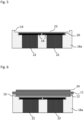
- FIG. 1 shows, in a schematic manner, a cross-section through a power electronics module 10.
- the power electronics module 10 comprises a substrate 11 with a first metallization area 12 on one of its main surfaces.
- the substrate 11 may be a ceramic substrate with a metallization layer formed on one side.
- a common, uninterrupted joining layer 13 is formed on a surface of the first metallization area opposite the substrate 11.
- the joining layer 13 may be a solder layer, a sinter layer, an adhesive layer, or a layer prepared by diffusion soldering or diffusion bonding.
- a group comprising two power electronic devices 14 is arranged on top of the joining layer 13, a group comprising two power electronic devices 14 is arranged.
- the group of power electronic devices 14 may comprise at least one semiconductor power diode and/or at least one semiconductor power transistors.
- the joining layer 13 is uninterrupted in the sense that it does not comprise any intentional gaps and/or provides a direct electrical path between the power electronic devices 14 of the same group, irrespective of an electrical path provided by the
- a remaining gap G between the two power electronic devices 14 is very small. That is to say, the power electronic devices 14 are arranged more or less directly adjacent to one another in the first metallization area 12. In terms of absolute distance, this may mean that the remaining gap G between the two power electronic devices 14 is smaller than 1 mm, for example 0.5 mm or less. In terms of relative distance, this may mean that the remaining gap G between the two power electronic devices 14 is smaller than 10% or 5% of the width and/or length of the adjacent power electronic devices 14.
- each power electronic device 14 is joined to a metallization area using a separate joining layer 13 as detailed later.
- the joining layer 13 is substantially continuous, and preferably has no gap in an area located between two adjacent power electronic devices 14.
- the joining layer 13 is formed from a common body of joining material. For example, a single piece of material, such as a single solder preform, a single sintering preform, or a single adhesive tape, may be used.
- a paste-like joining material such as solder paste, sinter material, or liquid adhesive
- a continuous or patterned shape such as a cross, snowflake, or multiple dots.
- a continuous joining layer 13 is formed by putting the power electronic devices 14 on the previously dispensed joining material.
- Figure 2 shows a top view of a power electronics module 10 with a total of five power electronic devices 14a to 14e, for three IGBTs (or other type of transistors) and two diodes.
- a first part 15, in Figure 2 the lower part covers a substantial part of the substrate 11, e.g. more than 50 percent of the total surface of the substrate 11, and comprises an essentially rectangular subarea 16, indicated using a dashed line, of a first metallization area 12.
- the subarea 16 represents the largest rectangular subarea of the first metallization area 12.
- a large proportion of the subarea 16, e.g. more than 95 percent, is covered by the five power electronic devices 14a to 14e. Only a remaining outer area of the subarea 16 near the outer edges of the five power electronic devices 14a to 14e is left uncovered.
- a smaller, second part 17 of the substrate 11, in Figure 2 the upper part may comprise further parts of the first metallization area and further metallization areas.
- metal traces used for connecting contact surfaces on the back side of the power electronic devices 14a to 14e and/or for connecting the power electronics modules 10 to other components or for joining of other electronic devices like sensor devices, passive device, control devices may be provided.
- the proportion of the subarea 16 can be at least 80 to 85 percent in some other variants of the power electronics module, e.g. when the shape of the subarea is other than the rectangular geometrical shape or when the current rating requirement is lower.
- further metallization areas and/or subareas may be provided.
- two different metallization areas may be provided for placement of one or more high-side group and one or more low-side group of power electronic devices, respectively (not shown).
- further metallization areas and corresponding groups of power electronic devices may be provided.
- one or more respective subareas for placement of power electronic devices may only cover a smaller part of the substrate's surface, but may still represent the largest continuous geometrical shape, such as a rectangle, of the respective metallization.
- the individual power electronic devices 14a to 14e touch each other or are separated only by a very narrow gap caused by the respective joining technique, as detailed below.
- the width of remaining gap G between the individual power electronic devices 14 is smaller than a width of a remaining outer edge E between the outside circumference of the first group of power electronic devices 14 and the respective outer circumference of the subarea 16.
- Figures 3 to 9 show how such a power electronics module may be formed by soldering.
- a modified solder fixture 18 is explained with reference to Figures 3 and 4 , before individual phases of a related manufacturing process are explained with reference to Figures 5 to 9 .
- Figures 3 and 4 show a perspective and a plane view of a first part 18a of the solder fixture 18, respectively.
- the first part 18a of the solder fixture 18 comprises a number of depressions for holding the components of power electronics module 10.
- a larger, relatively shallow first recess 19 corresponds to the outer circumference of the substrate 11 and/or the metallization areas formed thereon, and serves to hold the substrate 11 during soldering.
- a smaller, slightly deeper, second recess 20 is formed within the first recess 19, and is configured to hold a plurality of power electronic devices 14.
- the second recess 20 is configured to hold the five power electronic devices 14a to 14e previously shown in Figure 2 and a common solder preform, as explained later. While only a single second recess 20 configured for holding a single group of power electronic devices 14 is shown in Figures 3 and 4 , fixtures 18 comprising several second recesses 20 for multiple groups arranged on the same or different metallization areas 12 are also envisioned.
- the first part 18a of the solder fixture 18 comprises a number of further depressions, openings and other structural features that facilitate insertion and removal of the various components into and out of the solder fixture 18, and for accommodating weights for pushing down any power electronic devices 14 placed therein. For the sake of brevity, these are not described in detail here.
- a rectangular area 21 formed by the second recess 20 is highlighted using a dashed line. Attention is drawn to the fact that the edges of the second recess 20 corresponding to the rectangular area 21 serve to align all of the power electronic devices 14 and the common solder preform together. In contrast, no internal dividing or alignment features are provided between the positions of the individual power electronic devices 14a to 14e. Avoidance of such internal protrusions increases the space available for placement of the power electronic devices 14. Further attention is drawn to the fact that the rectangular area 21 formed within the second recess 20 essentially corresponds to or is only smaller by a relatively small fraction, e.g. a distance corresponding to a solder meniscus and/or needed for alignment, than the subarea 16 of the first metallization area 12.
- FIG. 5 shows, in a schematic manner, a first stage in the manufacturing of a power electronics module 10.
- multiple power electronic devices 14 have been placed in a common recess 20, from which only two are visible in the cross-section of Figures 5 to 9 .
- a corresponding weight 22 is arranged, which may be a loose part or may be attached to the first part 18a of the solder fixture 18 in a movable manner.
- solder preform 23 covers corresponding contact surfaces of the two power electronic devices 14 and essentially extends over the entire widths of the second recess 20. Accordingly, the same solder preform may be used, irrespective of the individual size of the used power electronic devices 14. For example, the same solder preform 23 may be used to attach two full-size or four half-size chips to the same metallization area 12. Attention is drawn once again to the fact that no separating protrusion is present between the two power electronic devices 14.
- Figure 6 shows a further stage in the manufacturing process.
- a double-sided substrate 11 comprising a first metallization area 12 on the first side and a second metallization area 24 arranged on the opposite, second side of the substrate 11 is placed in the first part 18a of the solder fixture 18.
- the first side may correspond to a backside
- the second side may correspond to a front side of the substrate 11.
- the first metallization area 12 is placed in the first recess 19 surrounding the second recess 20 such that a subarea of the first metallization area 12, for example the subarea 16 shown in Figure 2 , is aligned with the power electronic devices 14.
- a second part 18b of the solder fixture 18 (fixture bottom plate) is placed on top of the substrate 11, i.e. the second metallization area 24, to close the solder fixture 18.
- the closed solder fixture 18 comprising the first part 18a and the second part 18b is flipping, such that the weights 22 press the respective power electronic devices 14 against the first metallization area 12.
- the solder preform 23 is heated or otherwise liquefied, resulting in a layer of liquid solder material 25.
- a process gas or liquid such as hydrogen, or formic acid may be applied during soldering, to support or enable a chemical reduction of the solder material.
- hydrogen or formic acid may be used for reduction of the solder material of the solder preform 23.
- an inert gas like nitrogen may be applied during at least phases of the joining process.
- the solidified solder material 25 forms a common, uninterrupted solder layer 26 as shown in Figure 9 .
- the thickness of the solder layer 26 may vary to a small extend in areas below the power electronic devices 14 and neighbouring areas, e.g. by a limited overflow of the soldering material into the gap G or towards the edge E. Nonetheless, such a solder layer 26 may be described as homogenous, as it is formed in a single rather than several successive soldering steps.
- solder fixture 18 can be removed, with the individual power electronic devices 14 being mechanically and electrically attached to the first metallization area 12.
- the solder layer 26 may also serve as a thermal connection between the power electronic devices 14 and the substrate 11, e.g. for cooling of the power electronic devices 14. Due to the uninterrupted nature of the common joining layer 13 and/or the larger total surface area of the power electronic devices 14, the thermal capabilities of the resulting power electronics module 10 may also be improved, for example, by achieving a more uniform heat distribution.
- the individual power electronic devices 14 are essentially self-aligned by a solder meniscus 27 formed at the periphery of power electronic devices 14, e.g. by merging with the meniscus of an adjacent power electronic device 14, indicated by a recess 36 in the solder layer 26 in a remaining, internal gap between the power electronic devices 14, and a clear meniscus 27 on the outer periphery of the group of power electronic devices 14.
- the physical properties of the solder material itself provides an alignment aid, further alleviating the need for internal protrusions within the second depression 20 of the solder fixture 18.
- a controlled pressure may be applied to the power electronic devices 14, e.g. by corresponding fixtures.
- solder paste is coated on a surface of the first metallization area 12.
- a subarea intended for the placement of power electronic devices 14 may be covered with a patterned layer of a viscous solder paste by printing or coating or dispensing.
- the power electronic devices 14 of the first group are then mounted, for example, using a pick-and-place process and a subsequent thermal process, such as reflow soldering technique, resulting in a common, uninterrupted solder layer 26 as described above.
- use of a fixture for holding the power electronic devices 14 is optional, as the power electronic devices 14 may be held in place before and during soldering by the solder paste.
- each group can be mounted separately, as described below with respect to sintering.
- Figures 10 and 11 show an intermediate stage and resulting power electronics module 28 formed by an alternative, more conventional method of attaching two power electronic devices 14 to a substrate 11 with a first metallization area 12.
- each one of the power electronic devices 14 is individually aligned on all sides before and during soldering.
- a protrusion 29 is present in a first part 18a of a solder fixture 18, separating the power electronic devices 14 and individual solder preforms from each other. Accordingly, two separate solder preforms 23a and 23b must be placed in each one of two corresponding recesses 20a and 20b. During the soldering process, the power electronic devices 14 as well as the solder materials remain separated by the protrusion 29.
- two separate solder layers 26a and 26b are formed, which are separated from one another (except for unintentional solder overflows) by a corresponding gap G, which typically exceeds 1 mm in width.
- the surface area of the substrate 11 and corresponding part of the first metallization area 12 according to the gap G is lost for the placement of active components, so the chip sizes and consequently the active areas of the chips must be smaller. This leads to a lower current rating of the power electronics module 28 compared to the power electronics module 10 of Figure 9 .
- Figures 12 to 15 show, in a schematic manner, different stages of a manufacturing method for a power electronics module 10 based on sintering.
- a layer of sinter material is provided on a first metallization area 12 of a double-sided substrate 11.
- sintering preform 30 may be placed on the first metallization area 12.
- a layer of sinter material may be applied, for example by printing, in a corresponding area of the first metallization area 12.
- multiple power electronic devices 14, forming a group of power electronic devices to be sintered, are placed on the sintering preform 30.
- a pick and place procedure may be used to place individual power semiconductor chips on the sinter preform 30.
- the substrate 11 with the aligned power electronic device 14 may be placed in a sinter press.
- a protective foil 31 may be placed on top of the power electronic devices 14 to provide mechanical protection and/or protection against contaminations during sintering, e.g. to protect corresponding electrodes or other parts of the upper side of the power electronic devices 14.
- a first part 32a of a sintering fixture 32 may be placed over the protective foil 31, the power electronic devices 14, the sintering preform 30 and the double-sided substrate 11 as shown in Figure 13 .
- the first part 32a of a sintering fixture 32 comprises a recess 33 for laterally holding and/or aligning the power electronic device 14 before and during sintering.
- a second part 32b of the sintering press or sintering fixture 32 is arranged on the opposite side of the double-sided substrate 11, i.e. below the second metallization area 24, a second part 32b of the sintering press or sintering fixture 32 is arranged.
- sintering fixture is used here and a profiled sintering fixture 32 is shown for better understanding, attention is drawn to the fact that, in its simplest form, sintering may be performed between two arbitrary, flat surfaces. That is to say, the recess 33 represents an optional feature for the sintering process.
- the two opposite surfaces used for sintering are closed and pressed against each other to sinter the material of the sinter preform 30 into an essentially uniform sinter layer 34 between the power electronic devices 14 and the first metallization area 12.
- sintering based on mechanical pressing has been described above, other known sintering processes based on heat and/or a processing atmospheric may also be used or combined with a mechanical sintering process.
- sintering may be performed in an atmosphere consisting of an inert gas to avoid unwanted chemical reactions.
- the sintering layer 34 provides both a mechanical and electrical connection between the adjoining parts, and may also provide a thermal connection.
- the sintering fixture 32 may be removed and further processing steps may take place.
- one or more bond wires 35 may be connected to electrical contacts arranged on the opposite, upper surface of the individual power electronic devices 14, for example between different power electronic devices 14 as shown in Figure 15 , or between a power electronic device 14 and a metallization area (not shown). In this way, for example, a relatively large number of power electronic devices 14 may be connected electrically in parallel.
- a single, continuous and homogenous preform is used as solder or sinter material layer, respectively, which covers a large part of the outer surface of the first metallization area 12.
- different groups of power electronic devices 14 may be soldered or sintered to a common metallization area 12 in successive stages.
- a single preform or area covered with joining material such as a solder paste or sinter material, may only cover a part of the first metallization area 12, which corresponds to a respective first group of power electronic devices 14.
- a stack of multiple preforms and/or multiple layers of joining materials may be used.
- the above solder or sintering processed may be repeated for the second main surface of the substrate, thereby forming power electronics modules 10 carrying power electronic devices 14 on the two opposite metallization areas 12 and 24.
- a common, uninterrupted joining layer 13 may also be formed using an adhesive layer.
- a preferably electrically conductive, double-sided adhesive tape may be placed on an upper surface of a first metallization area 12 of a substrate 11. Thereafter, individual power electronic devices 14 forming a group of power electronic devices can be placed on the opposite second adhesive surface of the double-sided adhesive tape, e.g. by a pick and place process.
- a preferably electrically conductive, typically patterned layer of liquid or viscous glue such as a silver glue
- a preferably electrically conductive, typically patterned layer of liquid or viscous glue may be dispensed, for example in a patterned layer, by scribing, dispensing, printing or coating the liquid or viscous glue on the surface of the first metallization area 12, or on corresponding contact surfaces of a plurality of power electronic devices 14 held in a common fixture similar to the first part 18a of the solder fixture 18 shown in Figures 3 and 4 .
- the first metallization area 12 may be aligned with the group of power electronic devices 14.
- the liquid or viscous glue forms a homogenous layer.
- the glue may be cured using an appropriate process, such as heating or evaporating of a solvent, resulting an essentially homogenous, uninterrupted joining layer 13.
Landscapes
- Die Bonding (AREA)
Abstract
Description
- The present disclosure relates to a power electronics module comprising a substrate with at least a first metallization area and a first group of power electronic devices. The present disclosure further relates to a method for manufacturing such a power electronics module.
- Power electronics modules comprising a plurality of power electronic devices are used in many different application areas. In particular, in the area of power electronics, a plurality of power semiconductor chips may be connected in parallel to form a power electronics module with a relatively high current rating.
- With increasing demands for power density, it is desirable to increase the current rating of such power electronics modules. Increasing the power density can be achieved, for example, by the development and introduction of new chip technologies providing a reduction of conduction and switching losses of the individual semiconductor power devices during operation. However, the development of new chip technologies and their largescale manufacturing is very time consuming and costly, and therefore provides more of a long-term perspective. Accordingly, other means of increasing a current rating of a power electronics module are desirable.
- Embodiments of the disclosure relate to power electronics modules and methods for their manufacturing enabling an increased current rating of a power electronics module with a given size or, a smaller size of a power electronics module with a given current rating. This disclosure shows an alternative method with low effort to enhance or optimize the current capability.
- According to one aspect, a power electronics module comprises a substrate with at least a first metallization area, a first group of power electronic devices arranged in the first metallization area, and a common, uninterrupted joining layer arranged between the first metallization area and the first group of power electronic devices. The first group comprising a plurality of power electronic devices, and the common, uninterrupted joining layer establishes a mechanical and an electrical contact between the first metallization area and the first group of power electronic devices.
- Among others, the inventors have found that, by omitting or reducing a distance between power electronic devices and joining a plurality of power electronic devices using a common, uninterrupted joining layer to a single metallization area, a total active area of the power electronic devices arranged on a power electronics module of a given size can be increased, thereby also increasing a current rating of the power electronic devices. While the space on a substrate available for positioning of power electronic devices, such as semiconductor chips, is limited, it can be better utilized by joining multiple power electronic devices using a common, uninterrupted joining layer. This is in contrast to the joining of each power electronic device separately using a separate joining layer, where space is lost due to spaces between individual power electronic devices.
- According to at least one implementation, each one of the power electronic devices of the first group is arranged directly adjacent to at least one other power electronic device of the first group. In other words, the power electronic devices of the first group are arranged essentially without any gap, or at least a strongly reduced gap, between them, thus maximizing the use of available mounting space. By removing unused space between power electronic devices, the size of the power electronic devices, and consequently the active area can be increased. In particular, when power electronic devices, such as semiconductor chips, can be arranged very close to each other without significant empty space between them, an optimal use of the available surface area of the substrate can be obtained.
- According to at least one implementation, the power electronic devices may be self-aligned and/or the distance between adjacent power electronic devices of the first group is smaller than 1 mm, and in particular smaller than 0.5 mm. Such distances cannot be obtained using conventional mounting techniques, when power electronic devices are aligned and mounted using separate joining layers.
- According to at least one implementation, the first metallization area comprises a subarea covering a part of the first metallization area and/or the substrate, and the common, uninterrupted joining layer covers essentially the entire subarea.
- The area covered by the common, uninterrupted joining layer may exclude any space required for alignment of the group of power electronic devices. The subarea may represent a substantial part of the first metallization area or the substrate, such as the entire area available for placement of power electronic devices. For example, it may represent more than 25, 50 or 75 percent of the main surface area of the first metallization area or the substrate. The subarea may be a rectangular area or an area with any other geometry defined by the power electronic devices to be placed on the power module. For example, the subarea may be a largest rectangular part of the first metallization area. The subarea may exclude one or more smaller parts of the first metallization area configured for interconnecting the power electronic devices and/or for further components of the power electronics modules.
- According to different implementations, the power electronic devices of the first group may be joined to the first metallization area using different joining techniques, including soldering, diffusion soldering, diffusion bonding, sintering or gluing.
- In case the power electronic devices are soldered to the substrate, a solder layer may act as the common, uninterrupted joining layer. Moreover, due to the physical properties of a soldering process, a distance between neighboring power electronic devices of the first group may be defined by a solder meniscus. This effectively enables a self-alignment of the power electronic devices.
- In case the power electronic devices are sintered to the substrate, the common, uninterrupted joining layer may be implemented as a sinter layer of essentially uniform thickness.
- In case the power electronic devices are glued to the substrate, the common, uninterrupted joining layer may comprise an adhesive layer, in particular a double-sided adhesive tape or a continuous layer of scribed or printed glue.
- According to at least one implementation, the power electronic devices of the first group comprise semiconductor chips, such as MOSFETs, MISFETs, JFETs, IGBTs, or diodes.
- According to at least one implementation, each one of the semiconductor chips may comprise at least two terminals, and the terminals of each one of the semiconductor chips may be connected electrically in parallel. Combining multiple semiconductor chips in parallel enables a high current rating.
- According to different implementations, the power electronic devices of the first group may be of the same type, or may be of two or more different types. For example, a combination of one or more protective or free-wheeling diodes and one or more transistor or switching devices may be arranged on the first metallization area to form a hybrid power electronics module.
- According to another aspect, a method for manufacturing a power electronics module comprises:
- arranging a layer of joining material, in particular a single preform, between a first metallization area of a substrate and respective contact surfaces of a first group of power electronic devices, wherein the first group comprises a plurality of power electronic devices; and
- forming a common, uninterrupted joining layer from the joining material, wherein the common, uninterrupted joining layer establishes at least a mechanical and an electrical contact between the first metallization area and the first group of power electronic devices.
- The above method step enable result in a power electronics module with a high current density as detailed above.
- Depending on the used joining technique, e.g. soldering, diffusion soldering, diffusion bonding, sintering or gluing, different processing steps may be performed to process and join the plurality of power electronic devices of the first group together, thereby lowering manufacturing cost and improving yield.
- The present disclosure comprises several aspects of a power electronics module and methods for its manufacturing. Every feature described with respect to one of the aspects is also disclosed herein with respect to the other aspects, even if the respective feature is not explicitly mentioned in the context of the specific aspect.
- The accompanying figures are included to provide a further understanding. In the figures, elements of the same structure and/or functionality may be referenced by the same reference signs. It is to be understood that the embodiments shown in the figures are illustrative representations and are not necessarily drawn to scale.
-
Figure 1 shows a schematic cross-section through a power electronics module with a common, uninterrupted joining layer. -
Figure 2 shows a top view of a power electronics module comprising five power electronic devices with a common, uninterrupted joining layer. -
Figures 3 and 4 show different views of a solder fixture used for manufacturing a power electronics module. -
Figures 5 to 9 show a method for manufacturing a power electronics module by soldering. -
Figures 10 and 11 show a method for manufacturing a conventional power electronics module by soldering. -
Figures 12 to 15 show a method for manufacturing a power electronics module by sintering. - While the disclosure is amenable to various modifications and alternative forms, specifics thereof are shown by way of example in the figures and will be described in detail below. It should be understood, however, that the intention is not to limit the disclosure to the particular embodiments described. On the contrary, the intention is to cover all modifications, equivalents, and alternatives falling within the scope of the invention as defined by the appended set of claims.
-
Figure 1 shows, in a schematic manner, a cross-section through apower electronics module 10. Thepower electronics module 10 comprises asubstrate 11 with afirst metallization area 12 on one of its main surfaces. For example, thesubstrate 11 may be a ceramic substrate with a metallization layer formed on one side. A common, uninterrupted joininglayer 13 is formed on a surface of the first metallization area opposite thesubstrate 11. As detailed later, the joininglayer 13 may be a solder layer, a sinter layer, an adhesive layer, or a layer prepared by diffusion soldering or diffusion bonding. On top of the joininglayer 13, a group comprising two powerelectronic devices 14 is arranged. The group of powerelectronic devices 14 may comprise at least one semiconductor power diode and/or at least one semiconductor power transistors. The joininglayer 13 is uninterrupted in the sense that it does not comprise any intentional gaps and/or provides a direct electrical path between the powerelectronic devices 14 of the same group, irrespective of an electrical path provided by thefirst metallization area 12. - Attention is drawn to the fact that a remaining gap G between the two power
electronic devices 14 is very small. That is to say, the powerelectronic devices 14 are arranged more or less directly adjacent to one another in thefirst metallization area 12. In terms of absolute distance, this may mean that the remaining gap G between the two powerelectronic devices 14 is smaller than 1 mm, for example 0.5 mm or less. In terms of relative distance, this may mean that the remaining gap G between the two powerelectronic devices 14 is smaller than 10% or 5% of the width and/or length of the adjacent powerelectronic devices 14. - Such distances between adjacent power
electronic devices 14 cannot be achieved using conventional manufacturing methods, wherein each powerelectronic device 14 is joined to a metallization area using a separate joininglayer 13 as detailed later. Inversely, this means that the joininglayer 13 is substantially continuous, and preferably has no gap in an area located between two adjacent powerelectronic devices 14. Put differently, the joininglayer 13 is formed from a common body of joining material. For example, a single piece of material, such as a single solder preform, a single sintering preform, or a single adhesive tape, may be used. Alternatively, a paste-like joining material, such as solder paste, sinter material, or liquid adhesive, may be applied by dispensing or printing it in a continuous or patterned shape, such as a cross, snowflake, or multiple dots. A continuous joininglayer 13 is formed by putting the powerelectronic devices 14 on the previously dispensed joining material. -
Figure 2 shows a top view of apower electronics module 10 with a total of five powerelectronic devices 14a to 14e, for three IGBTs (or other type of transistors) and two diodes. Afirst part 15, inFigure 2 the lower part, covers a substantial part of thesubstrate 11, e.g. more than 50 percent of the total surface of thesubstrate 11, and comprises an essentiallyrectangular subarea 16, indicated using a dashed line, of afirst metallization area 12. - In the depicted embodiment, the
subarea 16 represents the largest rectangular subarea of thefirst metallization area 12. A large proportion of thesubarea 16, e.g. more than 95 percent, is covered by the five powerelectronic devices 14a to 14e. Only a remaining outer area of thesubarea 16 near the outer edges of the five powerelectronic devices 14a to 14e is left uncovered. A smaller,second part 17 of thesubstrate 11, inFigure 2 the upper part, may comprise further parts of the first metallization area and further metallization areas. For example, metal traces used for connecting contact surfaces on the back side of the powerelectronic devices 14a to 14e and/or for connecting thepower electronics modules 10 to other components or for joining of other electronic devices like sensor devices, passive device, control devices may be provided. The proportion of thesubarea 16 can be at least 80 to 85 percent in some other variants of the power electronics module, e.g. when the shape of the subarea is other than the rectangular geometrical shape or when the current rating requirement is lower. - In other embodiments, further metallization areas and/or subareas may be provided. For example, in a half-bridge used for an inverter module, two different metallization areas may be provided for placement of one or more high-side group and one or more low-side group of power electronic devices, respectively (not shown). For multi-phase inverters, further metallization areas and corresponding groups of power electronic devices may be provided. In such configurations, one or more respective subareas for placement of power electronic devices may only cover a smaller part of the substrate's surface, but may still represent the largest continuous geometrical shape, such as a rectangle, of the respective metallization.
- In the embodiment shown in
Figure 2 , the individual powerelectronic devices 14a to 14e touch each other or are separated only by a very narrow gap caused by the respective joining technique, as detailed below. In the embodiment shown inFigure 2 , the width of remaining gap G between the individual powerelectronic devices 14 is smaller than a width of a remaining outer edge E between the outside circumference of the first group of powerelectronic devices 14 and the respective outer circumference of thesubarea 16. -
Figures 3 to 9 show how such a power electronics module may be formed by soldering. At first, a modifiedsolder fixture 18 is explained with reference toFigures 3 and 4 , before individual phases of a related manufacturing process are explained with reference toFigures 5 to 9 . -
Figures 3 and 4 show a perspective and a plane view of afirst part 18a of thesolder fixture 18, respectively. As can be best seen inFigure 3 , thefirst part 18a of thesolder fixture 18 comprises a number of depressions for holding the components ofpower electronics module 10. In particular, a larger, relatively shallowfirst recess 19 corresponds to the outer circumference of thesubstrate 11 and/or the metallization areas formed thereon, and serves to hold thesubstrate 11 during soldering. - A smaller, slightly deeper,
second recess 20 is formed within thefirst recess 19, and is configured to hold a plurality of powerelectronic devices 14. In the described example, thesecond recess 20 is configured to hold the five powerelectronic devices 14a to 14e previously shown inFigure 2 and a common solder preform, as explained later. While only a singlesecond recess 20 configured for holding a single group of powerelectronic devices 14 is shown inFigures 3 and 4 ,fixtures 18 comprising severalsecond recesses 20 for multiple groups arranged on the same ordifferent metallization areas 12 are also envisioned. - The
first part 18a of thesolder fixture 18 comprises a number of further depressions, openings and other structural features that facilitate insertion and removal of the various components into and out of thesolder fixture 18, and for accommodating weights for pushing down any powerelectronic devices 14 placed therein. For the sake of brevity, these are not described in detail here. - In the top view of
Figure 4 , arectangular area 21 formed by thesecond recess 20 is highlighted using a dashed line. Attention is drawn to the fact that the edges of thesecond recess 20 corresponding to therectangular area 21 serve to align all of the powerelectronic devices 14 and the common solder preform together. In contrast, no internal dividing or alignment features are provided between the positions of the individual powerelectronic devices 14a to 14e. Avoidance of such internal protrusions increases the space available for placement of the powerelectronic devices 14. Further attention is drawn to the fact that therectangular area 21 formed within thesecond recess 20 essentially corresponds to or is only smaller by a relatively small fraction, e.g. a distance corresponding to a solder meniscus and/or needed for alignment, than thesubarea 16 of thefirst metallization area 12. -
Figure 5 shows, in a schematic manner, a first stage in the manufacturing of apower electronics module 10. At this stage, multiple powerelectronic devices 14 have been placed in acommon recess 20, from which only two are visible in the cross-section ofFigures 5 to 9 . Below each one of the powerelectronic devices 14, a correspondingweight 22 is arranged, which may be a loose part or may be attached to thefirst part 18a of thesolder fixture 18 in a movable manner. - In the described embodiment, above the two power
electronic devices 14, a single,continuous solder preform 23 is placed. Due to its larger size and the fact that only asingle solder preform 23 needs to be placed in thesolder fixture 18, handling of thepreform 23 and thus the entire manufacturing process may be simplified. Thesolder preform 23 covers corresponding contact surfaces of the two powerelectronic devices 14 and essentially extends over the entire widths of thesecond recess 20. Accordingly, the same solder preform may be used, irrespective of the individual size of the used powerelectronic devices 14. For example, thesame solder preform 23 may be used to attach two full-size or four half-size chips to thesame metallization area 12. Attention is drawn once again to the fact that no separating protrusion is present between the two powerelectronic devices 14. -
Figure 6 shows a further stage in the manufacturing process. At this stage, a double-sided substrate 11 comprising afirst metallization area 12 on the first side and asecond metallization area 24 arranged on the opposite, second side of thesubstrate 11 is placed in thefirst part 18a of thesolder fixture 18. For example, in a power module, the first side may correspond to a backside, and the second side may correspond to a front side of thesubstrate 11. In the depicted embodiment, thefirst metallization area 12 is placed in thefirst recess 19 surrounding thesecond recess 20 such that a subarea of thefirst metallization area 12, for example thesubarea 16 shown inFigure 2 , is aligned with the powerelectronic devices 14. - At a next stage, shown in
Figure 7 , asecond part 18b of the solder fixture 18 (fixture bottom plate) is placed on top of thesubstrate 11, i.e. thesecond metallization area 24, to close thesolder fixture 18. - Thereafter, as shown in
Figure 8 , theclosed solder fixture 18 comprising thefirst part 18a and thesecond part 18b is flipping, such that theweights 22 press the respective powerelectronic devices 14 against thefirst metallization area 12. At this stage, thesolder preform 23 is heated or otherwise liquefied, resulting in a layer ofliquid solder material 25. - Optionally, a process gas or liquid, such as hydrogen, or formic acid may be applied during soldering, to support or enable a chemical reduction of the solder material. For example, hydrogen or formic acid may be used for reduction of the solder material of the
solder preform 23. Alternatively, or additionally, an inert gas like nitrogen may be applied during at least phases of the joining process. - Once the soldering process is complete, the solidified
solder material 25 forms a common,uninterrupted solder layer 26 as shown inFigure 9 . The thickness of thesolder layer 26 may vary to a small extend in areas below the powerelectronic devices 14 and neighbouring areas, e.g. by a limited overflow of the soldering material into the gap G or towards the edge E. Nonetheless, such asolder layer 26 may be described as homogenous, as it is formed in a single rather than several successive soldering steps. - Thereafter, the
solder fixture 18 can be removed, with the individual powerelectronic devices 14 being mechanically and electrically attached to thefirst metallization area 12. Moreover, thesolder layer 26 may also serve as a thermal connection between the powerelectronic devices 14 and thesubstrate 11, e.g. for cooling of the powerelectronic devices 14. Due to the uninterrupted nature of the common joininglayer 13 and/or the larger total surface area of the powerelectronic devices 14, the thermal capabilities of the resultingpower electronics module 10 may also be improved, for example, by achieving a more uniform heat distribution. - As can be seen in
Figure 9 , due to the surface tension of the liquid solder material, the individual powerelectronic devices 14 are essentially self-aligned by asolder meniscus 27 formed at the periphery of powerelectronic devices 14, e.g. by merging with the meniscus of an adjacent powerelectronic device 14, indicated by arecess 36 in thesolder layer 26 in a remaining, internal gap between the powerelectronic devices 14, and aclear meniscus 27 on the outer periphery of the group of powerelectronic devices 14. In this way, the physical properties of the solder material itself provides an alignment aid, further alleviating the need for internal protrusions within thesecond depression 20 of thesolder fixture 18. - While a conventional soldering process has been described, more advanced soldering techniques, such as diffusion soldering may also be used accordingly. In this case, rather than
weights 22, a controlled pressure may be applied to the powerelectronic devices 14, e.g. by corresponding fixtures. - Moreover, in another embodiment, instead of placing a
solder preform 23 in thecommon recess 20, solder paste is coated on a surface of thefirst metallization area 12. For example, a subarea intended for the placement of powerelectronic devices 14 may be covered with a patterned layer of a viscous solder paste by printing or coating or dispensing. The powerelectronic devices 14 of the first group are then mounted, for example, using a pick-and-place process and a subsequent thermal process, such as reflow soldering technique, resulting in a common,uninterrupted solder layer 26 as described above. In this case, use of a fixture for holding the powerelectronic devices 14 is optional, as the powerelectronic devices 14 may be held in place before and during soldering by the solder paste. - Finally, in case more than one group of power
electronic devices 14 shall be mounted, each group can be mounted separately, as described below with respect to sintering. -
Figures 10 and 11 show an intermediate stage and resultingpower electronics module 28 formed by an alternative, more conventional method of attaching two powerelectronic devices 14 to asubstrate 11 with afirst metallization area 12. - As shown in
Figure 10 , each one of the powerelectronic devices 14 is individually aligned on all sides before and during soldering. To this end, aprotrusion 29 is present in afirst part 18a of asolder fixture 18, separating the powerelectronic devices 14 and individual solder preforms from each other. Accordingly, two separate solder preforms 23a and 23b must be placed in each one of two corresponding recesses 20a and 20b. During the soldering process, the powerelectronic devices 14 as well as the solder materials remain separated by theprotrusion 29. - Accordingly, as is shown in
Figure 11 , twoseparate solder layers substrate 11 and corresponding part of thefirst metallization area 12 according to the gap G is lost for the placement of active components, so the chip sizes and consequently the active areas of the chips must be smaller. This leads to a lower current rating of thepower electronics module 28 compared to thepower electronics module 10 ofFigure 9 . - That is to say, when using a common, uninterrupted joining
layer 13, larger and/or more numerous chips forming the powerelectronic devices 14 may be placed incommon metallization area 12 of a given size. This results in a larger total active area of the chips, which in turn results in a higher current capability or power density. Inversely, if the number and size of the individual powerelectronic devices 14 is fixed, asmaller substrate 11 with asmaller metallization area 12 may be used to obtain the same current capability. This may result in a miniaturization and reduction of cost. -
Figures 12 to 15 show, in a schematic manner, different stages of a manufacturing method for apower electronics module 10 based on sintering. - At a first stage, shown in
Figure 12 , a layer of sinter material is provided on afirst metallization area 12 of a double-sided substrate 11. As an example, sinteringpreform 30 may be placed on thefirst metallization area 12. Alternatively, a layer of sinter material may be applied, for example by printing, in a corresponding area of thefirst metallization area 12. - At a next stage, shown in
Figure 13 , multiple powerelectronic devices 14, forming a group of power electronic devices to be sintered, are placed on thesintering preform 30. For example, a pick and place procedure may be used to place individual power semiconductor chips on thesinter preform 30. - The
substrate 11 with the aligned powerelectronic device 14 may be placed in a sinter press. In an optional step, aprotective foil 31 may be placed on top of the powerelectronic devices 14 to provide mechanical protection and/or protection against contaminations during sintering, e.g. to protect corresponding electrodes or other parts of the upper side of the powerelectronic devices 14. For example, afirst part 32a of asintering fixture 32 may be placed over theprotective foil 31, the powerelectronic devices 14, thesintering preform 30 and the double-sided substrate 11 as shown inFigure 13 . As shown inFigure 13 , thefirst part 32a of asintering fixture 32 comprises arecess 33 for laterally holding and/or aligning the powerelectronic device 14 before and during sintering. On the opposite side of the double-sided substrate 11, i.e. below thesecond metallization area 24, asecond part 32b of the sintering press or sinteringfixture 32 is arranged. - While the term "sintering fixture" is used here and a profiled
sintering fixture 32 is shown for better understanding, attention is drawn to the fact that, in its simplest form, sintering may be performed between two arbitrary, flat surfaces. That is to say, therecess 33 represents an optional feature for the sintering process. - As shown in
Figure 14 , the two opposite surfaces used for sintering are closed and pressed against each other to sinter the material of thesinter preform 30 into an essentiallyuniform sinter layer 34 between the powerelectronic devices 14 and thefirst metallization area 12. - While sintering based on mechanical pressing has been described above, other known sintering processes based on heat and/or a processing atmospheric may also be used or combined with a mechanical sintering process. For example, sintering may be performed in an atmosphere consisting of an inert gas to avoid unwanted chemical reactions.
- As detailed above, the
sintering layer 34 provides both a mechanical and electrical connection between the adjoining parts, and may also provide a thermal connection. - Once the sintering is complete, as shown in
Figure 15 , thesintering fixture 32 may be removed and further processing steps may take place. For example, as also shown inFigure 15 , one ormore bond wires 35 may be connected to electrical contacts arranged on the opposite, upper surface of the individual powerelectronic devices 14, for example between different powerelectronic devices 14 as shown inFigure 15 , or between a powerelectronic device 14 and a metallization area (not shown). In this way, for example, a relatively large number of powerelectronic devices 14 may be connected electrically in parallel. - In the scenario shown in
Figures 1 to 9 andFigures 12 to 15 , a single, continuous and homogenous preform is used as solder or sinter material layer, respectively, which covers a large part of the outer surface of thefirst metallization area 12. However, in other embodiments (not shown), different groups of powerelectronic devices 14 may be soldered or sintered to acommon metallization area 12 in successive stages. In this case, a single preform or area covered with joining material, such as a solder paste or sinter material, may only cover a part of thefirst metallization area 12, which corresponds to a respective first group of powerelectronic devices 14. - Moreover, especially in the case of sintering, depending on the joining materials and joining processes, a stack of multiple preforms and/or multiple layers of joining materials may be used.
- Moreover, although not shown in the drawings, the above solder or sintering processed may be repeated for the second main surface of the substrate, thereby forming
power electronics modules 10 carrying powerelectronic devices 14 on the twoopposite metallization areas - The embodiments shown in
Figures 1 to 9 and12 to 15 as stated represent exemplary embodiments of improvedpower electronics modules 10 and methods for their manufacturing. Therefore, they do not constitute a complete list of all embodiments according to the improved devices and methods. Actual devices and methods may vary from the embodiments shown in terms of arrangements, devices and processing steps, for example. - For example, while not shown in the attached figures, a common, uninterrupted joining
layer 13 may also be formed using an adhesive layer. For example, a preferably electrically conductive, double-sided adhesive tape may be placed on an upper surface of afirst metallization area 12 of asubstrate 11. Thereafter, individual powerelectronic devices 14 forming a group of power electronic devices can be placed on the opposite second adhesive surface of the double-sided adhesive tape, e.g. by a pick and place process. Alternatively, a preferably electrically conductive, typically patterned layer of liquid or viscous glue, such as a silver glue, may be dispensed, for example in a patterned layer, by scribing, dispensing, printing or coating the liquid or viscous glue on the surface of thefirst metallization area 12, or on corresponding contact surfaces of a plurality of powerelectronic devices 14 held in a common fixture similar to thefirst part 18a of thesolder fixture 18 shown inFigures 3 and 4 . Thereafter, thefirst metallization area 12 may be aligned with the group of powerelectronic devices 14. As a result, the liquid or viscous glue forms a homogenous layer. After placement of the powerelectronic devices 14 the glue may be cured using an appropriate process, such as heating or evaporating of a solvent, resulting an essentially homogenous, uninterrupted joininglayer 13. -
- 10
- power electronics module
- 11
- substrate
- 12
- first metallization area
- 13
- joining layer
- 14
- power electronic device
- 15
- first part (of substrate)
- 16
- subarea
- 17
- second part (of substrate)
- 18
- solder fixture
- 18a
- first part of solder fixture
- 18b
- second part of solder fixture
- 19
- first recess
- 20
- second recess
- 21
- rectangular area
- 22
- weight
- 23
- solder preform
- 24
- second metallization area
- 25
- solder material
- 26
- solder layer
- 27
- solder meniscus
- 28
- power electronics module
- 29
- protrusion
- 30
- sintering preform
- 31
- protective foil
- 32
- sintering fixture
- 33
- recess
- 34
- sinter layer
- 35
- bond wire
- 36
- recess
- G
- gap
- E
- edge
Claims (15)
- A power electronics module (10), comprising:- a substrate (11) with at least a first metallization area (12) ;- a first group of power electronic devices (14) arranged in the first metallization area (12), wherein the first group comprises a plurality of power electronic devices (14); and- a common, uninterrupted joining layer (13) arranged between the first metallization area (12) and the first group of power electronic devices (14), wherein the common, uninterrupted joining layer (13) establishes at least a mechanical and an electrical contact between the first metallization area (12) and the first group of power electronic devices (14).
- The power electronics module (10) of claim 1, wherein each one of the power electronic devices (14) of the first group is arranged directly adjacent to at least one other power electronic device (14) of the first group.
- The power electronics module (10) of claim 1 or 2, wherein the power electronic devices (14) are self-aligned and/or a distance between adjacent power electronic devices (14) of the first group is smaller than 1 mm, and in particular smaller than 0.5 mm.
- The power electronics module (10) of any one of claims 1 to 3, wherein the first metallization area (12) comprises a subarea (16) covering a part of the first metallization area (12) and/or the substrate (11), and the common, uninterrupted joining layer (13) covers essentially the entire subarea (16).
- The power electronics module (10) of claim 4, wherein a distance between an outer circumference of the rectangular subarea (16) and an outer edge of a closest power electronic device (14) of the first group is larger than a distance between adjacent power electronic devices (14) of the first group.
- The power electronics module (10) of any one of claims 1 to 5, wherein the common, uninterrupted joining layer (13) comprises a solder layer (26), and a distance between neighboring power electronic devices (14) of the first group is defined by the solder meniscus (27).
- The power electronics module (10) of any one of claims 1 to 5, wherein the common, uninterrupted joining layer (13) comprises one of a sinter layer (34) of essentially uniform thickness and an adhesive layer, in particular a double-sided adhesive tape or a layer of conductive scribed, printed, or coated glue.
- The power electronics module (10) of any one of claims 1 to 7, wherein the power electronic devices (14) of the first group are semiconductor chips, comprising at least one of a MOSFET, a MISFET, a JFET, an IBGT or a diode.
- The power electronics module (10) of claim 8, wherein each one of the semiconductor chips comprises at least two terminals, and the terminals of each one of the chips are connected electrically in parallel.
- The power electronics module (10) of any one of claims 1 to 9, wherein the first group of power electronic devices (14) comprises at least two different types of power electronic devices arranged in the first metallization area (12).
- A method for manufacturing a power electronics module (10), comprising:- arranging a layer of joining material, in particular a single preform, between a first metallization area (12) of a substrate (11) and respective contact surfaces of a first group of power electronic devices (14), wherein the first group comprises a plurality of power electronic devices (14); and- forming a common, uninterrupted joining layer (13) from the joining material, wherein the common, uninterrupted joining layer (13) establishes at least a mechanical and an electrical contact between the first metallization area (12) and the first group of power electronic devices (14).
- The method of claim 11, wherein the layer of joining material comprises a solder preform (23), and the method specifically comprises:- placing the first group of power electronic devices (14) in a common recess (20) of a first part (18a) of a solder fixture (18), the common recess (20) being free of protrusions for separating power electronic devices (14) of the first group;- placing the solder preform (23) on the contact surfaces of the power electronic devices (14) of the first group;- placing the substrate (11) with the at least one metallization area (12) on the solder preform (23);- closing the solder fixture (18); and- applying a solder process to transform the continuous solder preform (23) to a common, uninterrupted solder layer (26).
- The method of claim 11, wherein the layer of joining material comprises a layer of solder paste, and the method specifically comprises:- coating at least a part of the first metallization area (12) with a layer of solder paste;- placing the first group of power electronic devices (14) on the layer of solder paste; and- applying a solder process to transform the solder paste to a common, uninterrupted solder layer (26).
- The method of claim 11, wherein the layer of joining material comprises at least one sinter preform (30) or layer of sinter material, and the method specifically comprises:- placing the at least one sinter preform (30) on the first metallization area (12) of the substrate (11) or coating at least a part of the first metallization area (12) with a layer of sinter material;- placing the power electronic devices (14) of the first group on the at least one sinter preform (30) or layer of sinter material; and- applying at least one of pressure, heat and a processing atmosphere to sinter the at least one sinter preform (30) or layer of sinter material to form a common, uninterrupted sinter layer (34).
- The method of claim 11, wherein the layer of joining material comprises an adhesive material, in particular a conductive adhesive material, and the method specifically comprises:- placing the adhesive material on the first metallization area of the substrate, comprising at least one of attaching a double-sided adhesive tape to the first metallization area (12) and scribing, printing, dispensing or coating a continuous and/or patterned glue layer onto the first metallization area (12); and- placing the power electronic devices of the first group on the adhesive material.
Priority Applications (3)
| Application Number | Priority Date | Filing Date | Title |
|---|---|---|---|
| EP22155917.2A EP4227995B1 (en) | 2022-02-09 | 2022-02-09 | Power electronics module and method for its manufacturing |
| PCT/EP2023/053068 WO2023152160A1 (en) | 2022-02-09 | 2023-02-08 | Power electronics module and method for its manufacture |
| CN202380020781.8A CN118891726A (en) | 2022-02-09 | 2023-02-08 | Power electronic module and method for manufacturing the same |
Applications Claiming Priority (1)
| Application Number | Priority Date | Filing Date | Title |
|---|---|---|---|
| EP22155917.2A EP4227995B1 (en) | 2022-02-09 | 2022-02-09 | Power electronics module and method for its manufacturing |
Publications (2)
| Publication Number | Publication Date |
|---|---|
| EP4227995A1 true EP4227995A1 (en) | 2023-08-16 |
| EP4227995B1 EP4227995B1 (en) | 2024-09-11 |
Family
ID=80446487
Family Applications (1)
| Application Number | Title | Priority Date | Filing Date |
|---|---|---|---|
| EP22155917.2A Active EP4227995B1 (en) | 2022-02-09 | 2022-02-09 | Power electronics module and method for its manufacturing |
Country Status (3)
| Country | Link |
|---|---|
| EP (1) | EP4227995B1 (en) |
| CN (1) | CN118891726A (en) |
| WO (1) | WO2023152160A1 (en) |
Cited By (2)
| Publication number | Priority date | Publication date | Assignee | Title |
|---|---|---|---|---|
| WO2025226298A1 (en) * | 2024-04-25 | 2025-10-30 | Microchip Technology Incorporated | Semiconductor device and method for manufacturing same |
| EP4645384A1 (en) * | 2024-04-24 | 2025-11-05 | Hyundai Mobis Co., Ltd. | Transport apparatus for semiconductor manufacturing |
Citations (3)
| Publication number | Priority date | Publication date | Assignee | Title |
|---|---|---|---|---|
| DE19735531A1 (en) * | 1997-08-16 | 1999-02-18 | Abb Research Ltd | Power semiconductor module with coolers integrated in submodules |
| US6002163A (en) * | 1998-01-02 | 1999-12-14 | General Electric Company | Electronic device pad relocation, precision placement, and packaging in arrays |
| EP2804209A1 (en) * | 2013-05-17 | 2014-11-19 | ABB Technology AG | Moulded electronics module |
Family Cites Families (4)
| Publication number | Priority date | Publication date | Assignee | Title |
|---|---|---|---|---|
| DE102008048869A1 (en) * | 2008-09-25 | 2010-04-22 | Infineon Technologies Ag | Device and method for connecting two connection partners |
| US20190287943A1 (en) * | 2015-08-31 | 2019-09-19 | Delta Electronics (Shanghai) Co., Ltd | Power package module of multiple power chips and method of manufacturing power chip unit |
| DE102016106137B4 (en) * | 2016-04-04 | 2023-12-28 | Infineon Technologies Ag | Electronic device housing comprising a dielectric layer and an encapsulating material |
| US10074590B1 (en) * | 2017-07-02 | 2018-09-11 | Infineon Technologies Ag | Molded package with chip carrier comprising brazed electrically conductive layers |
-
2022
- 2022-02-09 EP EP22155917.2A patent/EP4227995B1/en active Active
-
2023
- 2023-02-08 WO PCT/EP2023/053068 patent/WO2023152160A1/en not_active Ceased
- 2023-02-08 CN CN202380020781.8A patent/CN118891726A/en active Pending
Patent Citations (3)
| Publication number | Priority date | Publication date | Assignee | Title |
|---|---|---|---|---|
| DE19735531A1 (en) * | 1997-08-16 | 1999-02-18 | Abb Research Ltd | Power semiconductor module with coolers integrated in submodules |
| US6002163A (en) * | 1998-01-02 | 1999-12-14 | General Electric Company | Electronic device pad relocation, precision placement, and packaging in arrays |
| EP2804209A1 (en) * | 2013-05-17 | 2014-11-19 | ABB Technology AG | Moulded electronics module |
Cited By (2)
| Publication number | Priority date | Publication date | Assignee | Title |
|---|---|---|---|---|
| EP4645384A1 (en) * | 2024-04-24 | 2025-11-05 | Hyundai Mobis Co., Ltd. | Transport apparatus for semiconductor manufacturing |
| WO2025226298A1 (en) * | 2024-04-25 | 2025-10-30 | Microchip Technology Incorporated | Semiconductor device and method for manufacturing same |
Also Published As
| Publication number | Publication date |
|---|---|
| WO2023152160A1 (en) | 2023-08-17 |
| CN118891726A (en) | 2024-11-01 |
| EP4227995B1 (en) | 2024-09-11 |
Similar Documents
| Publication | Publication Date | Title |
|---|---|---|
| US12094793B2 (en) | Package with electrically insulated carrier and at least one step on encapsulant | |
| US9530707B2 (en) | Semiconductor module | |
| US10204882B2 (en) | Stacked package module having an exposed heat sink surface from the packaging | |
| EP3690938B1 (en) | Semiconductor device and production method therefor | |
| CN102437138B (en) | Semiconductor device | |
| EP2662892B1 (en) | Stacked interposer leadframes | |
| EP2889902B1 (en) | Electric power semiconductor device | |
| EP4227995B1 (en) | Power electronics module and method for its manufacturing | |
| US9437508B2 (en) | Method for manufacturing semiconductor device and semiconductor device | |
| US12293955B2 (en) | High power module package structures | |
| TW202110289A (en) | Power module | |
| EP1137065A2 (en) | Semiconductor device and manufacturing method thereof | |
| US20240178094A1 (en) | Semiconductor package | |
| EP1696484B1 (en) | Process for assembling a double-sided circuit component | |
| US11322430B2 (en) | Semiconductor device and semiconductor module with a highest portion of a terminal lower than a highest portion of the mold sealing resin | |
| US11222878B2 (en) | Electronic power module | |
| JP2002076175A (en) | Semiconductor package and manufacturing method thereof | |
| EP2722885B1 (en) | Surface mountable power components | |
| CN114005758A (en) | Surface mounting packaging method and packaging structure of power module | |
| US20250218887A1 (en) | Semiconductor device and manufacturing method of semiconductor device | |
| US20250054840A1 (en) | Power module having a lead frame that provides substrate support and forms terminals of the power module | |
| US20260082944A1 (en) | Semiconductor device and method for manufacturing the same | |
| EP4428914A1 (en) | Power semiconductor module arrangement | |
| KR102724106B1 (en) | Power Module Connected by Multi-layer and the Manufacturing Method thereof | |
| EP4113605A1 (en) | Power semiconductor module arrangement |
Legal Events
| Date | Code | Title | Description |
|---|---|---|---|
| STAA | Information on the status of an ep patent application or granted ep patent |
Free format text: STATUS: EXAMINATION IS IN PROGRESS |
|
| PUAI | Public reference made under article 153(3) epc to a published international application that has entered the european phase |
Free format text: ORIGINAL CODE: 0009012 |
|
| 17P | Request for examination filed |
Effective date: 20220923 |
|
| AK | Designated contracting states |
Kind code of ref document: A1 Designated state(s): AL AT BE BG CH CY CZ DE DK EE ES FI FR GB GR HR HU IE IS IT LI LT LU LV MC MK MT NL NO PL PT RO RS SE SI SK SM TR |
|
| RAP1 | Party data changed (applicant data changed or rights of an application transferred) |
Owner name: HITACHI ENERGY LTD |
|
| GRAP | Despatch of communication of intention to grant a patent |
Free format text: ORIGINAL CODE: EPIDOSNIGR1 |
|
| STAA | Information on the status of an ep patent application or granted ep patent |
Free format text: STATUS: GRANT OF PATENT IS INTENDED |
|
| INTG | Intention to grant announced |
Effective date: 20240411 |
|
| GRAS | Grant fee paid |
Free format text: ORIGINAL CODE: EPIDOSNIGR3 |
|
| P01 | Opt-out of the competence of the unified patent court (upc) registered |
Free format text: CASE NUMBER: APP_38560/2024 Effective date: 20240627 |
|
| GRAA | (expected) grant |
Free format text: ORIGINAL CODE: 0009210 |
|
| STAA | Information on the status of an ep patent application or granted ep patent |
Free format text: STATUS: THE PATENT HAS BEEN GRANTED |
|
| AK | Designated contracting states |
Kind code of ref document: B1 Designated state(s): AL AT BE BG CH CY CZ DE DK EE ES FI FR GB GR HR HU IE IS IT LI LT LU LV MC MK MT NL NO PL PT RO RS SE SI SK SM TR |
|
| REG | Reference to a national code |
Ref country code: GB Ref legal event code: FG4D |
|
| REG | Reference to a national code |
Ref country code: CH Ref legal event code: EP |
|
| REG | Reference to a national code |
Ref country code: DE Ref legal event code: R096 Ref document number: 602022005941 Country of ref document: DE |
|
| REG | Reference to a national code |
Ref country code: IE Ref legal event code: FG4D |
|
| REG | Reference to a national code |
Ref country code: DE Ref legal event code: R079 Ref document number: 602022005941 Country of ref document: DE Free format text: PREVIOUS MAIN CLASS: H01L0025070000 Ipc: H10D0080200000 |
|
| REG | Reference to a national code |
Ref country code: LT Ref legal event code: MG9D |
|
| PG25 | Lapsed in a contracting state [announced via postgrant information from national office to epo] |
Ref country code: NO Free format text: LAPSE BECAUSE OF FAILURE TO SUBMIT A TRANSLATION OF THE DESCRIPTION OR TO PAY THE FEE WITHIN THE PRESCRIBED TIME-LIMIT Effective date: 20241211 |
|
| REG | Reference to a national code |
Ref country code: NL Ref legal event code: MP Effective date: 20240911 |
|
| PG25 | Lapsed in a contracting state [announced via postgrant information from national office to epo] |
Ref country code: GR Free format text: LAPSE BECAUSE OF FAILURE TO SUBMIT A TRANSLATION OF THE DESCRIPTION OR TO PAY THE FEE WITHIN THE PRESCRIBED TIME-LIMIT Effective date: 20241212 Ref country code: FI Free format text: LAPSE BECAUSE OF FAILURE TO SUBMIT A TRANSLATION OF THE DESCRIPTION OR TO PAY THE FEE WITHIN THE PRESCRIBED TIME-LIMIT Effective date: 20240911 |
|
| PG25 | Lapsed in a contracting state [announced via postgrant information from national office to epo] |
Ref country code: BG Free format text: LAPSE BECAUSE OF FAILURE TO SUBMIT A TRANSLATION OF THE DESCRIPTION OR TO PAY THE FEE WITHIN THE PRESCRIBED TIME-LIMIT Effective date: 20240911 |
|
| PG25 | Lapsed in a contracting state [announced via postgrant information from national office to epo] |
Ref country code: LV Free format text: LAPSE BECAUSE OF FAILURE TO SUBMIT A TRANSLATION OF THE DESCRIPTION OR TO PAY THE FEE WITHIN THE PRESCRIBED TIME-LIMIT Effective date: 20240911 |
|
| PG25 | Lapsed in a contracting state [announced via postgrant information from national office to epo] |
Ref country code: HR Free format text: LAPSE BECAUSE OF FAILURE TO SUBMIT A TRANSLATION OF THE DESCRIPTION OR TO PAY THE FEE WITHIN THE PRESCRIBED TIME-LIMIT Effective date: 20240911 |
|
| PG25 | Lapsed in a contracting state [announced via postgrant information from national office to epo] |
Ref country code: ES Free format text: LAPSE BECAUSE OF FAILURE TO SUBMIT A TRANSLATION OF THE DESCRIPTION OR TO PAY THE FEE WITHIN THE PRESCRIBED TIME-LIMIT Effective date: 20240911 Ref country code: RS Free format text: LAPSE BECAUSE OF FAILURE TO SUBMIT A TRANSLATION OF THE DESCRIPTION OR TO PAY THE FEE WITHIN THE PRESCRIBED TIME-LIMIT Effective date: 20241211 |
|
| PG25 | Lapsed in a contracting state [announced via postgrant information from national office to epo] |
Ref country code: RS Free format text: LAPSE BECAUSE OF FAILURE TO SUBMIT A TRANSLATION OF THE DESCRIPTION OR TO PAY THE FEE WITHIN THE PRESCRIBED TIME-LIMIT Effective date: 20241211 Ref country code: NO Free format text: LAPSE BECAUSE OF FAILURE TO SUBMIT A TRANSLATION OF THE DESCRIPTION OR TO PAY THE FEE WITHIN THE PRESCRIBED TIME-LIMIT Effective date: 20241211 Ref country code: LV Free format text: LAPSE BECAUSE OF FAILURE TO SUBMIT A TRANSLATION OF THE DESCRIPTION OR TO PAY THE FEE WITHIN THE PRESCRIBED TIME-LIMIT Effective date: 20240911 Ref country code: HR Free format text: LAPSE BECAUSE OF FAILURE TO SUBMIT A TRANSLATION OF THE DESCRIPTION OR TO PAY THE FEE WITHIN THE PRESCRIBED TIME-LIMIT Effective date: 20240911 Ref country code: GR Free format text: LAPSE BECAUSE OF FAILURE TO SUBMIT A TRANSLATION OF THE DESCRIPTION OR TO PAY THE FEE WITHIN THE PRESCRIBED TIME-LIMIT Effective date: 20241212 Ref country code: FI Free format text: LAPSE BECAUSE OF FAILURE TO SUBMIT A TRANSLATION OF THE DESCRIPTION OR TO PAY THE FEE WITHIN THE PRESCRIBED TIME-LIMIT Effective date: 20240911 Ref country code: ES Free format text: LAPSE BECAUSE OF FAILURE TO SUBMIT A TRANSLATION OF THE DESCRIPTION OR TO PAY THE FEE WITHIN THE PRESCRIBED TIME-LIMIT Effective date: 20240911 Ref country code: BG Free format text: LAPSE BECAUSE OF FAILURE TO SUBMIT A TRANSLATION OF THE DESCRIPTION OR TO PAY THE FEE WITHIN THE PRESCRIBED TIME-LIMIT Effective date: 20240911 |
|
| REG | Reference to a national code |
Ref country code: AT Ref legal event code: MK05 Ref document number: 1723485 Country of ref document: AT Kind code of ref document: T Effective date: 20240911 |
|
| PG25 | Lapsed in a contracting state [announced via postgrant information from national office to epo] |
Ref country code: NL Free format text: LAPSE BECAUSE OF FAILURE TO SUBMIT A TRANSLATION OF THE DESCRIPTION OR TO PAY THE FEE WITHIN THE PRESCRIBED TIME-LIMIT Effective date: 20240911 |
|
| PG25 | Lapsed in a contracting state [announced via postgrant information from national office to epo] |
Ref country code: PT Free format text: LAPSE BECAUSE OF FAILURE TO SUBMIT A TRANSLATION OF THE DESCRIPTION OR TO PAY THE FEE WITHIN THE PRESCRIBED TIME-LIMIT Effective date: 20250113 Ref country code: IS Free format text: LAPSE BECAUSE OF FAILURE TO SUBMIT A TRANSLATION OF THE DESCRIPTION OR TO PAY THE FEE WITHIN THE PRESCRIBED TIME-LIMIT Effective date: 20250111 |
|
| PG25 | Lapsed in a contracting state [announced via postgrant information from national office to epo] |
Ref country code: SM Free format text: LAPSE BECAUSE OF FAILURE TO SUBMIT A TRANSLATION OF THE DESCRIPTION OR TO PAY THE FEE WITHIN THE PRESCRIBED TIME-LIMIT Effective date: 20240911 |
|
| PG25 | Lapsed in a contracting state [announced via postgrant information from national office to epo] |
Ref country code: EE Free format text: LAPSE BECAUSE OF FAILURE TO SUBMIT A TRANSLATION OF THE DESCRIPTION OR TO PAY THE FEE WITHIN THE PRESCRIBED TIME-LIMIT Effective date: 20240911 Ref country code: AT Free format text: LAPSE BECAUSE OF FAILURE TO SUBMIT A TRANSLATION OF THE DESCRIPTION OR TO PAY THE FEE WITHIN THE PRESCRIBED TIME-LIMIT Effective date: 20240911 |
|
| PG25 | Lapsed in a contracting state [announced via postgrant information from national office to epo] |
Ref country code: CZ Free format text: LAPSE BECAUSE OF FAILURE TO SUBMIT A TRANSLATION OF THE DESCRIPTION OR TO PAY THE FEE WITHIN THE PRESCRIBED TIME-LIMIT Effective date: 20240911 Ref country code: PL Free format text: LAPSE BECAUSE OF FAILURE TO SUBMIT A TRANSLATION OF THE DESCRIPTION OR TO PAY THE FEE WITHIN THE PRESCRIBED TIME-LIMIT Effective date: 20240911 |
|
| PG25 | Lapsed in a contracting state [announced via postgrant information from national office to epo] |
Ref country code: SK Free format text: LAPSE BECAUSE OF FAILURE TO SUBMIT A TRANSLATION OF THE DESCRIPTION OR TO PAY THE FEE WITHIN THE PRESCRIBED TIME-LIMIT Effective date: 20240911 Ref country code: IT Free format text: LAPSE BECAUSE OF FAILURE TO SUBMIT A TRANSLATION OF THE DESCRIPTION OR TO PAY THE FEE WITHIN THE PRESCRIBED TIME-LIMIT Effective date: 20240911 |
|
| REG | Reference to a national code |
Ref country code: DE Ref legal event code: R097 Ref document number: 602022005941 Country of ref document: DE |
|
| PG25 | Lapsed in a contracting state [announced via postgrant information from national office to epo] |
Ref country code: DK Free format text: LAPSE BECAUSE OF FAILURE TO SUBMIT A TRANSLATION OF THE DESCRIPTION OR TO PAY THE FEE WITHIN THE PRESCRIBED TIME-LIMIT Effective date: 20240911 |
|
| PLBE | No opposition filed within time limit |
Free format text: ORIGINAL CODE: 0009261 |
|
| STAA | Information on the status of an ep patent application or granted ep patent |
Free format text: STATUS: NO OPPOSITION FILED WITHIN TIME LIMIT |
|
| 26N | No opposition filed |
Effective date: 20250612 |
|
| PG25 | Lapsed in a contracting state [announced via postgrant information from national office to epo] |
Ref country code: SE Free format text: LAPSE BECAUSE OF FAILURE TO SUBMIT A TRANSLATION OF THE DESCRIPTION OR TO PAY THE FEE WITHIN THE PRESCRIBED TIME-LIMIT Effective date: 20240911 |
|
| PG25 | Lapsed in a contracting state [announced via postgrant information from national office to epo] |
Ref country code: MC Free format text: LAPSE BECAUSE OF FAILURE TO SUBMIT A TRANSLATION OF THE DESCRIPTION OR TO PAY THE FEE WITHIN THE PRESCRIBED TIME-LIMIT Effective date: 20240911 |
|
| REG | Reference to a national code |
Ref country code: CH Ref legal event code: PL |
|
| PG25 | Lapsed in a contracting state [announced via postgrant information from national office to epo] |
Ref country code: LU Free format text: LAPSE BECAUSE OF NON-PAYMENT OF DUE FEES Effective date: 20250209 |
|
| PG25 | Lapsed in a contracting state [announced via postgrant information from national office to epo] |
Ref country code: CH Free format text: LAPSE BECAUSE OF NON-PAYMENT OF DUE FEES Effective date: 20250228 |
|
| REG | Reference to a national code |
Ref country code: BE Ref legal event code: MM Effective date: 20250228 |
|
| PG25 | Lapsed in a contracting state [announced via postgrant information from national office to epo] |
Ref country code: FR Free format text: LAPSE BECAUSE OF NON-PAYMENT OF DUE FEES Effective date: 20250228 |
|
| PG25 | Lapsed in a contracting state [announced via postgrant information from national office to epo] |
Ref country code: BE Free format text: LAPSE BECAUSE OF NON-PAYMENT OF DUE FEES Effective date: 20250228 |
|
| PG25 | Lapsed in a contracting state [announced via postgrant information from national office to epo] |
Ref country code: IE Free format text: LAPSE BECAUSE OF NON-PAYMENT OF DUE FEES Effective date: 20250209 |
|
| PGFP | Annual fee paid to national office [announced via postgrant information from national office to epo] |
Ref country code: DE Payment date: 20260218 Year of fee payment: 5 |
|
| PG25 | Lapsed in a contracting state [announced via postgrant information from national office to epo] |
Ref country code: RO Free format text: LAPSE BECAUSE OF FAILURE TO SUBMIT A TRANSLATION OF THE DESCRIPTION OR TO PAY THE FEE WITHIN THE PRESCRIBED TIME-LIMIT Effective date: 20240911 |