EP4227810A1 - Methods for managing communications involving a lockstep processing system - Google Patents
Methods for managing communications involving a lockstep processing system Download PDFInfo
- Publication number
- EP4227810A1 EP4227810A1 EP23168417.6A EP23168417A EP4227810A1 EP 4227810 A1 EP4227810 A1 EP 4227810A1 EP 23168417 A EP23168417 A EP 23168417A EP 4227810 A1 EP4227810 A1 EP 4227810A1
- Authority
- EP
- European Patent Office
- Prior art keywords
- signal
- data synchronizer
- processing lane
- processing
- lockstep
- Prior art date
- Legal status (The legal status is an assumption and is not a legal conclusion. Google has not performed a legal analysis and makes no representation as to the accuracy of the status listed.)
- Pending
Links
Images




Classifications
-
- G—PHYSICS
- G06—COMPUTING OR CALCULATING; COUNTING
- G06F—ELECTRIC DIGITAL DATA PROCESSING
- G06F13/00—Interconnection of, or transfer of information or other signals between, memories, input/output devices or central processing units
- G06F13/38—Information transfer, e.g. on bus
- G06F13/42—Bus transfer protocol, e.g. handshake; Synchronisation
- G06F13/4204—Bus transfer protocol, e.g. handshake; Synchronisation on a parallel bus
- G06F13/4221—Bus transfer protocol, e.g. handshake; Synchronisation on a parallel bus being an input/output bus, e.g. ISA bus, EISA bus, PCI bus, SCSI bus
- G06F13/423—Bus transfer protocol, e.g. handshake; Synchronisation on a parallel bus being an input/output bus, e.g. ISA bus, EISA bus, PCI bus, SCSI bus with synchronous protocol
-
- G—PHYSICS
- G06—COMPUTING OR CALCULATING; COUNTING
- G06F—ELECTRIC DIGITAL DATA PROCESSING
- G06F11/00—Error detection; Error correction; Monitoring
- G06F11/07—Responding to the occurrence of a fault, e.g. fault tolerance
- G06F11/16—Error detection or correction of the data by redundancy in hardware
- G06F11/1675—Temporal synchronisation or re-synchronisation of redundant processing components
- G06F11/1683—Temporal synchronisation or re-synchronisation of redundant processing components at instruction level
-
- G—PHYSICS
- G06—COMPUTING OR CALCULATING; COUNTING
- G06F—ELECTRIC DIGITAL DATA PROCESSING
- G06F11/00—Error detection; Error correction; Monitoring
- G06F11/07—Responding to the occurrence of a fault, e.g. fault tolerance
- G06F11/16—Error detection or correction of the data by redundancy in hardware
- G06F11/1629—Error detection by comparing the output of redundant processing systems
- G06F11/1641—Error detection by comparing the output of redundant processing systems where the comparison is not performed by the redundant processing components
- G06F11/1645—Error detection by comparing the output of redundant processing systems where the comparison is not performed by the redundant processing components and the comparison itself uses redundant hardware
-
- G—PHYSICS
- G06—COMPUTING OR CALCULATING; COUNTING
- G06F—ELECTRIC DIGITAL DATA PROCESSING
- G06F11/00—Error detection; Error correction; Monitoring
- G06F11/07—Responding to the occurrence of a fault, e.g. fault tolerance
- G06F11/16—Error detection or correction of the data by redundancy in hardware
- G06F11/1675—Temporal synchronisation or re-synchronisation of redundant processing components
-
- G—PHYSICS
- G06—COMPUTING OR CALCULATING; COUNTING
- G06F—ELECTRIC DIGITAL DATA PROCESSING
- G06F11/00—Error detection; Error correction; Monitoring
- G06F11/07—Responding to the occurrence of a fault, e.g. fault tolerance
- G06F11/16—Error detection or correction of the data by redundancy in hardware
- G06F11/1608—Error detection by comparing the output signals of redundant hardware
- G06F11/1616—Error detection by comparing the output signals of redundant hardware where the redundant component is an I/O device or an adapter therefor
-
- G—PHYSICS
- G06—COMPUTING OR CALCULATING; COUNTING
- G06F—ELECTRIC DIGITAL DATA PROCESSING
- G06F13/00—Interconnection of, or transfer of information or other signals between, memories, input/output devices or central processing units
- G06F13/38—Information transfer, e.g. on bus
- G06F13/42—Bus transfer protocol, e.g. handshake; Synchronisation
- G06F13/4204—Bus transfer protocol, e.g. handshake; Synchronisation on a parallel bus
- G06F13/4208—Bus transfer protocol, e.g. handshake; Synchronisation on a parallel bus being a system bus, e.g. VME bus, Futurebus, Multibus
- G06F13/4217—Bus transfer protocol, e.g. handshake; Synchronisation on a parallel bus being a system bus, e.g. VME bus, Futurebus, Multibus with synchronous protocol
Definitions
- the present subject matter relates generally to lockstep processing systems.
- Processor systems used for critical real-time processing applications have inherent problems in determining when a hardware failure has occurred and taking subsequent corrective action.
- One method of detecting such failures and maintaining consistent operation is to use a lockstep processing system having redundant processors. In such situations, the processors each perform the same exact instruction at the same time. This is called lockstep processing. If a mismatch between the inputs or the outputs of the processors exists, the processors are no longer operating in lockstep with one another.
- the lockstep processing system has its drawbacks.
- asynchronous inputs to the lockstep processing system will generally fail. Whenever asynchronous signals are sampled, there are times when the input signal will change during the sampling time. When this occurs, there is a probability that the input signals change may not be seen by one of the processors. As an example, when the input signal causes a processor interrupt to occur, one processor may respond to the interrupt and start execution of an interrupt service routine before the other processor. Hence, the two processors will not remain in lockstep even though a hardware fault has not occurred.
- a method for managing communications involving a lockstep processing comprising at least a first processor and a second processor can include receiving, at a data synchronizer, a first signal from a first device.
- the method can also include receiving, at the data synchronizer, a second signal from a second device.
- the method can include determining, by the data synchronizer, whether the first signal is equal to the second signal.
- the method can include transmitting, by the data synchronizer, the first signal to the first processor and the second signal to the second processor.
- transmitting the first signal to the first processor can occur synchronously with transmitting the second signal to the second processor.
- communications involving a lockstep processing system comprising at least a first processor and a second processor can be managed by a data synchronizer having a first processing lane and a second processing lane.
- the data synchronizer can be configured to receive a first signal at the first processing lane.
- the data synchronizer can also be configured to transmit the first data signal to the second processing lane.
- the data synchronizer can be configured to transmit the first signal from the first processing lane to the lockstep processing system.
- the data synchronizer can also be configured to transmit the second signal from the second processing lane to the lockstep processing system.
- transmitting the first signal from the first processing lane to the lockstep processing system occurs synchronously with transmitting the second signal from the second processing lane to the lockstep processing system.
- a method for managing communications involving a lockstep processing system comprising at least a first processor and a second processor can include receiving, at a first processing lane of a data synchronizer, a first signal from a first device.
- the method can also include transmitting, by the data synchronizer, the first signal from the first processing lane to a second processing lane of the data synchronizer.
- the method can include transmitting, by the data synchronizer, the first signal from the first processing lane to the lockstep processing system.
- the method can also include transmitting, by the data synchronizer, the first signal from the second processing lane to the lockstep processing system.
- transmission of the first signal from the first processing lane to the lockstep processing system occurs synchronously with transmission of the first signal from the second processing lane to the lockstep processing system.
- first and second can be used interchangeably to distinguish one component from another and are not intended to signify location or importance of the individual components.
- the singular forms “a”, “an”, and “the” include plural references unless the context clearly dictates otherwise.
- the lockstep processing system can include at least a first processor and a second processor.
- the first and second processors can both operate in a lockstep mode in which the first processor and the second processor both execute the same set of instructions.
- a data synchronizer can be communicatively coupled to the lockstep processing system.
- the data synchronizer can manage communications between the lockstep processing system and one or more devices, such as memory controllers.
- the data synchronizer can include a first processing lane and a second processing lane communicatively coupled to one another via a cross-channel interface.
- one or more signals entering the data synchronizer at the first processing lane can be transmitted to the second processing lane via the cross-channel interface.
- one or more signals entering the data synchronizer at the second processing lane can be transmitted to the first processing lane via the cross-channel interface.
- the data synchronizer can compare signals between the two processing lanes.
- the data synchronizer can be configured to synchronously transmit the signals to the lockstep processing system. In this way, the data synchronizer can ensure the first and second processors of the lockstep processing system both operate in a lockstep mode in which the first and second processors execute the same set of instructions.
- the data synchronizer and methods of using the data synchronizer according to example aspects of the present disclosure can have a number of technical effects and benefits.
- example aspects of the present disclosure have a technical effect of improving integrity of data transferred to and from the lockstep processing system.
- the reliability of lockstep processing systems used in avionics systems for aerial vehicles and other applications can be improved.
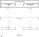
- FIG. 1 depicts an example embodiment of a system 100 for managing communications involving a lockstep processing system 110.
- the lockstep processing system 110 can include a first processor 112 and a second processor 114.
- the lockstep processing system 110 can include three or more processors. It should be appreciated, however, that both the first processor 112 and the second processor 114 each operate in a lockstep mode in which the first and second processors 112, 114 each synchronously execute the same set of instructions.
- the system 100 can include a data synchronizer 120 comprising a first processing lane 122 and a second processing lane 124.
- the data synchronizer 120 can be communicatively coupled to a first device 130 and a second device 132.
- the first device 130 can be in communication with the first processing lane 122
- the second device 132 can be in communication with the second processing lane 124.
- the first processing lane 122 can receive one or more signals originating from the first device 130
- the second processing lane 124 can receive one or more signals originating from the second device 132.
- the data synchronizer 120 can be communicatively coupled to the lockstep processing system 110. More specifically, the first processor 112 can be communicatively coupled to the first processing lane 122, and the second processor 114 can be communicatively coupled to the second processing lane 124. In this way, the first processing lane 122 can receive one or more signals originating from the first processor 112, and the second processing lane 124 can receive one or more signals originating from the second processor 114. Likewise, the first processor 112 can receive one or more signals from the first processing lane 122, and the second processor 114 can receive one or more signals from the second processing lane 124. As will be discussed below in more detail, the data synchronizer 120 can manage communications between the lockstep processing system 110 and at least one of the first and second devices 130, 132.
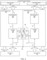
- example embodiments of the data synchronizer 120 can include a cross-channel interface 126 to provide communications between the first processing lane 122 and the second processing lane 124. In this way, one or more signals entering the data synchronizer 120 at the first processing lane 122 can be communicated to the second processing lane 124. Likewise, one or more signals entering the data synchronizer 120 at the second processing lane 124 can be communicated to the first processing lane 122.
- the data synchronizer 120 can receive a first signal S 1 and a second signal S 2 .
- the first signal S 1 can originate from the first device 130
- the second signal S 2 can originate from the second device 132.
- the first signal S 1 can enter the data synchronizer 120 at the first processing lane 122
- the second signal S 2 can enter the data synchronizer 120 at the second processing lane 124.
- first and second signals S 1 and S 2 can be any suitable signal.
- the first signal S 1 can be an address read (AR) signal originating from the first device 130.
- the second signal S 2 can be an address write (AW) signal originating from the second device 132.
- the first signal S 1 , the second signal S 2 , or both can be a write (W) signal.
- the first signal S 1 can be transmitted from the first processing lane 122 to the second processing lane 124 via the cross-channel interface 126.
- the second signal S 2 can be transmitted from the second processing lane 124 to the first processing lane 122 via the cross-channel interface 126.
- the data synchronizer 120 can be configured to determine whether the first signal S 1 and second signal S 2 are equal to one another.
- both the first processing lane 122 and the second processing lane 124 can include compare logic 140 that, when executed, configures the data synchronizer 120 to compare the first and second signals S 1 and S 2 to one another.
- the compare logic 140 can implement any suitable method for determine whether the first signal S 1 and the second signal S 2 are equal to one another.
- the compare logic 140 when executed, can configure the data synchronizer 120 to correlate the first signal S 1 with the second signal S 2 to determine a correlation factor value that is indicative of a similarity between the first signal S 1 and the second signal S 1 .
- a correlation factor value of one (1) can indicate the first signal S 1 and the second signal S 2 are equal to one another.
- a correlation factor value of zero (0) can indicate the first signal S 1 and the second signal S 2 are not equal to one another.
- the data synchronizer 120 determines the first signal S 1 and the second signal S 2 are not equal to one another, then neither the first signal S 1 nor the second signal S 2 are transmitted to the lockstep processing system 110. Instead, the data synchronizer 120 can generate a first response signal (not shown) that is unique to the first signal S 1 . In addition, the data synchronizer 120 can generate a second response signal (also not shown) that is unique to the second signal S 2 . In one example embodiment, the first response signal can be generated for the first device 130, and the second response signal can be generated for the second device 132. In addition, the data synchronizer 120 can transmit the first response signal to the first device 130, and the second response signal to the second device 132.
- both the first processing lane 122 and the second processing lane 124 can include synchronization logic 160 that, when executed, configures the data synchronizer 120 to synchronously transmit the first signal S 1 to the first processor 112, and the second signal S 2 to the second processor 114.
- the first signal S 1 can be transmitted to the second processor 114
- the second signal S 2 can be transmitted to the first processor 112.
- the data synchronizer 120 can simultaneously receive a third signal S 3 and a fourth signal S 4 from the lockstep processing system 110.
- the first processor 112 can generate the third signal S 3 in response to receiving the first signal S 1 .
- the second processor 114 can generate the fourth signal S 4 in response to receiving the second signal S 2 .
- the third signal S 3 can enter the data synchronizer 120 at the first processing lane 122.
- the fourth signal S 4 can enter the data synchronizer 120 at the second processing lane 124.
- both the third and fourth signals S 3 and S 4 can be any suitable signal.
- both the third signal S 3 and the fourth signal S 4 can be a read data (R) signal.
- both the third and fourth signal S 3 and S 4 can be a write response (B) signal.
- the third signal S 3 can be transmitted from the first processing lane 122 to the second processing lane 124 via the cross-channel interface 126.
- the fourth signal S 4 can be transmitted from the second processing lane 124 to the first processing lane 122 via the cross-channel interface 126.
- the data synchronizer 120 can be configured to determine whether the third signal S 3 and the fourth signal S 4 are cycle accurate.
- the first processing lane 122 and the second processing lane 124 can each include compare logic 150.
- the third signal S 3 and the fourth signal S 4 can be inputs to the compare logic 150.
- the compare logic 150 when executed, can configure the data synchronizer 120 to compare the third and fourth signals S 3 and S 4 to one another.
- the compare logic 150 can include any suitable application specific integrated circuit (ASIC) configured for determining whether the third signal S 3 and the fourth signal S 4 are equal to one another.
- the compare logic 150 can include an exclusive OR gate. More specifically, the exclusive OR gate can generate a first value (e.g., 0) when the third signal S 3 and the fourth signal S 4 are equal to one another. In contrast, the exclusive OR gate can generate a second value (e.g., 1) when the third signal S 3 and the fourth signal S 4 are not equal to one another.
- the compare logic 150 when executed, can configure the data synchronizer 120 to determine whether the first processor 112 and second processor 114 are operating in the lockstep mode.
- the first processing lane 122 and the second processing lane 124 can each include decoding logic 152.
- the decoding logic 152 of the first processing lane 122 can receive the third signal S 3 as an input. In this way, the decoding logic 152 of the first processing lane 122 can decode the third signal S 3 to generate a decoded third signal S D3 .
- the decoding logic 152 of the second processing lane 124 can receive the fourth signal S 4 as an input. In this way, the decoding logic 152 of the second processing lane 124 can decode the fourth signal S 4 to generate a decoded fourth signal S D4 .
- the decoded third signal S D3 can be transmitted to the first device 130.
- the decoded fourth signal S D4 can be transmitted to the second device 132.
- the decoded third signal S D3 can be transmitted to the second device 132, and the decoded fourth signal S D4 can be transmitted to the first device 130.
- the compare logic 150 and the decoding logic 152 can be executed in parallel. As such, the third and fourth signal S 3 and S 4 can be decoded and simultaneously compared with one another. However, it should be appreciated that the compare logic 150 can be executed within a fewer number of clock cycles than the decoding logic 152. As such, if the data synchronizer 120 determines the third signal S 3 and the fourth signal S 4 are not equal to one another, the data synchronizer 120 can be configured to stop transmission of the decoded third and fourth signal S D3 and S D4 to the first device 130 and the second device 132, respectively.
- the system 100 of FIGS. 2 and 3 provides numerous technical advantages. For example, since the first processing lane 122 and the second processing lanes 124 are communicatively coupled to one another via the cross-channel interface 126, the data synchronizer 120 provides error checking across both the first and second processing lanes 122 and 124. In this way, the integrity of data transferred to and from the lockstep processing system 100 can be improved.
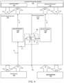
- FIG. 4 illustrates another example embodiment of a system 100 for managing communications involving the lockstep processing system 110.
- a first signal S 1 originating from the first device 130 can be received at the first processing lane 122 of the data synchronizer 120.
- the first signal S 1 can be an input to synchronization logic 160 of the first processing lane 122.
- the first signal S 1 can be transmitted to the second processing lane 124 via the cross-channel interface 126.
- the first signal S 1 can be transmitted to synchronization logic 160 of the second processing lane 124. In this way, the first signal S 1 can be synchronously transmitted to the lockstep processing system 110 in both the first processing lane 122 and the second processing lane 124.
- the lockstep processing system 110 can generate a second signal S 2 and a third signal S 3 in response to the first signal S 1 ( FIG. 4 ) received from the data synchronizer 120.
- the first processor 112 can generate the second signal S 2 in response to receiving the first signal S 1 .
- the second processor 114 can generate the third signal S 3 in response to receiving the first signal S 1 .
- the first processing lane 122 and the second processing lane 124 can simultaneously receive the second signal S 2 and a third signal S 3 , respectively.
- the second signal S 2 can enter the data synchronizer 120 at the first processing lane 122
- the third signal S 3 can enter the data synchronizer 120 at the second processing lane 124.
- both the second signal S 2 and the third signal S 3 can be any suitable signal.
- both the second signal S 2 and the third signal S 3 can be a read data (R) signal.
- both the second signal S 2 and the third signal S 3 can be a write response (B) signal.
- the second signal S 2 can be transmitted from the first processing lane 122 to the second processing lane 124 via the cross-channel interface 126.
- the third signal S 3 can be transmitted from the second processing lane 124 to the first processing lane 122 via the cross-channel interface 126.
- the data synchronizer 120 can be configured to determine whether the second signal S 2 and the third signal S 3 are cycle accurate.
- the first processing lane 122 and the second processing lane 124 can each include compare logic 150.
- the second signal S 2 and the third signal S 3 can be inputs to the compare logic 150.
- the compare logic 150 when executed, can configure the data synchronizer 120 to compare the second and third signals S 2 and S 3 to one another.
- the compare logic 150 can include any suitable application specific integrated circuit (ASIC) configured for determining whether the second signal S 2 and the third signal S 3 are equal to one another.
- the compare logic 150 can include an exclusive OR gate. More specifically, the exclusive OR gate can generate a first value (e.g., 0) when the second signal S 2 and the third signal S 3 are equal to one another. In contrast, the exclusive OR gate can generate a second value (e.g., 1) when the second signal S 2 and the third signal S 3 are not equal to one another.
- the compare logic 150 when executed, can configure the data synchronizer 120 to determine whether the first processor 112 and second processor 114 are operating in the lockstep mode.
- the first processing lane 122 and the second processing lane 124 can each include decoding logic 152.
- the decoding logic 152 of the first processing lane 122 can receive the second signal S 2 as an input. In this way, the decoding logic 152 of the first processing lane 122 can decode the second signal S 2 to generate a decoded second signal S D2 .
- the decoding logic 152 of the second processing lane 124 can receive the third signal S 3 as an input. In this way, the decoding logic 152 of the second processing lane 124 can decode the third signal S 3 to generate a decoded third signal S D3 .
- the decoded second signal S D2 can be transmitted to the first device 130.
- the decoded third signal S D3 can be transmitted to the second device 132.
- the decoded second signal S D2 can be transmitted to the second device 132, and the decoded third signal S D3 can be transmitted to the first device 130.
- the compare logic 150 and the decoding logic 152 can be executed in parallel. As such, the second and third signal S 2 and S 3 can be decoded and simultaneously compared with one another. However, it should be appreciated that the compare logic 150 can be executed within a fewer number of clock cycles than the decoding logic 152. As such, if the data synchronizer 120 determines the second signal S 2 and the third signal S 3 are not equal to one another, the data synchronizer 120 can be configured to stop transmission of the decoded second and third signal S D2 and S D3 to the first device 130 and the second device 132, respectively.
- FIG. 6 depicts another example embodiment of a system 100 for managing communications involving the lockstep processing system 110.
- the system 100 can include an interconnect fabric 116 to provide communications between the lockstep processing system 110 and the data synchronizer 120.
- the data synchronizer 120 can communicate with the lockstep processing system 110 through the interconnect fabric 116.
- the interconnect fabric 116 can receive one or more signals exiting the data synchronizer 120.
- the interconnect fabric 116 can communicate the one or more signals to the first processor 112, the second processor 114, or both.
- the system 100 of FIG. 6 has numerous advantages.
- the first processor 112 and the second processor 114 can each be replaced with processors designed for non-lockstep applications without sacrificing the performance and tight coupling between the processors and the interconnect fabric. Inn this way, software written for the processors can be executed unchanged in lockstep applications.
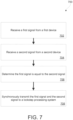
- FIG. 7 a flow diagram of one embodiment of a method 700 for managing communications involving a lockstep processing system in accordance with aspects of the present subject matter.
- the method 700 will be discussed herein with reference to the system(s) described above with reference to FIGS. 1-3 .
- FIG. 7 depicts steps performed in a particular order for purposes of illustration and discussion, the methods discussed herein are not limited to any particular order or arrangement.
- steps of the methods disclosed herein can be omitted, rearranged, combined, and/or adapted in various ways without deviating from the scope of the present disclosure.
- the method 700 can include receiving, at a data synchronizer, a first signal from a first device.
- the method 700 can include receiving, at the data synchronizer, a second signal from a second device.
- the data synchronizer can simultaneously receive the first and second signals from the first and second devices, respectively.
- the method 700 can include determining, by the data synchronizer, whether the first signal is equal to the second signal.
- the data synchronizer can compare the first signal with the second signal.
- the data synchronizer can calculate a correlation factor value that is indicative of a similarity between the first signal and the second signal.
- a correlation factor value of 1 can indicate the first and second signals are equal to one another.
- a correlation factor value of 0 can indicate the first and second signals are not equal to one another.
- the method 700 can include, at (708), transmitting, by the data synchronizer, the first signal to the first processor and the second signal to the second processor.
- transmission of the first signal can occur synchronously with the second signal.
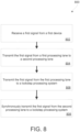
- FIG. 8 a flow diagram of one embodiment of a method 800 for managing communications involving a lockstep processing system in accordance with aspects of the present subject matter.
- the method 800 will be discussed herein with reference to the system(s) described above with reference to FIGS. 4 and 5 .
- FIG. 8 depicts steps performed in a particular order for purposes of illustration and discussion, the methods discussed herein are not limited to any particular order or arrangement.
- steps of the methods disclosed herein can be omitted, rearranged, combined, and/or adapted in various ways without deviating from the scope of the present disclosure.
- the method 800 can include receiving, at a data synchronizer, a first signal from a first device.
- the method 800 can include transmitting, by a cross-channel interface of the data synchronizer, the first signal to a second processing lane of the data synchronizer.
- the method 800 can include transmitting, by the data synchronizer, the first signal from the first processing lane to the lockstep processing system.
- the method 800 can include transmitting, by the data synchronizer, the first signal from the second processing lane to the lockstep processing system.
- transmission of the first signal at (806) can occur synchronously with transmission of the second signal at (808).
- the first signal can be transmitted from the first and second processing lanes to an interconnect fabric. More specifically, the interconnect fabric can be communicatively coupled to the data synchronizer and the lockstep processing system.
- example vehicles 900 according to example embodiments of the present disclosure are depicted.
- the systems and methods of the present disclosure can be implemented on an aerial vehicle 902, helicopter 904, automobile 906, boat 908, train 910, submarine 912 and/or any other suitable vehicles.
- One of ordinary skill in the art would understand that the systems and methods of the present disclosure can be implemented on other vehicles without deviating from the scope of the present disclosure.
Landscapes
- Engineering & Computer Science (AREA)
- Theoretical Computer Science (AREA)
- Physics & Mathematics (AREA)
- General Engineering & Computer Science (AREA)
- General Physics & Mathematics (AREA)
- Quality & Reliability (AREA)
- Hardware Redundancy (AREA)
- Selective Calling Equipment (AREA)
Abstract
Description
- The present subject matter relates generally to lockstep processing systems.
- Processor systems used for critical real-time processing applications have inherent problems in determining when a hardware failure has occurred and taking subsequent corrective action. One method of detecting such failures and maintaining consistent operation is to use a lockstep processing system having redundant processors. In such situations, the processors each perform the same exact instruction at the same time. This is called lockstep processing. If a mismatch between the inputs or the outputs of the processors exists, the processors are no longer operating in lockstep with one another.
- However, the lockstep processing system has its drawbacks. In particular, asynchronous inputs to the lockstep processing system will generally fail. Whenever asynchronous signals are sampled, there are times when the input signal will change during the sampling time. When this occurs, there is a probability that the input signals change may not be seen by one of the processors. As an example, when the input signal causes a processor interrupt to occur, one processor may respond to the interrupt and start execution of an interrupt service routine before the other processor. Hence, the two processors will not remain in lockstep even though a hardware fault has not occurred.
- Aspects and advantages of the present disclosure will be set forth in part in the following description, or may be obvious from the description, or may be learned through practice of the present disclosure.
- In one example aspect, a method for managing communications involving a lockstep processing comprising at least a first processor and a second processor can include receiving, at a data synchronizer, a first signal from a first device. The method can also include receiving, at the data synchronizer, a second signal from a second device. In addition, the method can include determining, by the data synchronizer, whether the first signal is equal to the second signal. When the first signal is equal to the second signal, the method can include transmitting, by the data synchronizer, the first signal to the first processor and the second signal to the second processor. Specifically, in example aspects, transmitting the first signal to the first processor can occur synchronously with transmitting the second signal to the second processor.
- In another example aspect, communications involving a lockstep processing system comprising at least a first processor and a second processor can be managed by a data synchronizer having a first processing lane and a second processing lane. The data synchronizer can be configured to receive a first signal at the first processing lane. The data synchronizer can also be configured to transmit the first data signal to the second processing lane. In addition, the data synchronizer can be configured to transmit the first signal from the first processing lane to the lockstep processing system. The data synchronizer can also be configured to transmit the second signal from the second processing lane to the lockstep processing system. Specifically, in example aspects, transmitting the first signal from the first processing lane to the lockstep processing system occurs synchronously with transmitting the second signal from the second processing lane to the lockstep processing system.
- In yet another example aspect, a method for managing communications involving a lockstep processing system comprising at least a first processor and a second processor can include receiving, at a first processing lane of a data synchronizer, a first signal from a first device. The method can also include transmitting, by the data synchronizer, the first signal from the first processing lane to a second processing lane of the data synchronizer. In addition, the method can include transmitting, by the data synchronizer, the first signal from the first processing lane to the lockstep processing system. The method can also include transmitting, by the data synchronizer, the first signal from the second processing lane to the lockstep processing system. Specifically, in example aspects, transmission of the first signal from the first processing lane to the lockstep processing system occurs synchronously with transmission of the first signal from the second processing lane to the lockstep processing system.
- These and other features, aspects and advantages of the present disclosure will become better understood with reference to the following description and appended claims. The accompanying drawings, which are incorporated in and constitute a part of this specification, illustrate aspects of the present disclosure and, together with the description, serve to explain the principles of the present disclosure.
- A full and enabling disclosure of the present disclosure, including the best mode thereof, directed to one of ordinary skill in the art, is set forth in the specification, which makes reference to the appended Figs., in which:
-
FIG. 1 illustrates an example system for managing communications involving a lockstep processing system according to example embodiments of the present disclosure; -
FIG. 2 illustrates a data synchronizer of the system depicted inFIG. 1 receiving a first signal and a second signal according to example embodiments of the present disclosure; -
FIG.3 illustrates the example data synchronizer ofFIG. 1 receiving a third signal and a fourth signal according to example embodiments of the present disclosure; -
FIG. 4 illustrates another example data synchronizer receiving a first signal according to example embodiments of the present disclosure; -
FIG. 5 illustrates the example data synchronizer ofFIG. 4 receiving a second signal and a third signal according to example embodiments of the present disclosure; -
FIG. 6 illustrates another example system for managing communications involving a lockstep processing system according to example embodiments of the present disclosure; -
FIG. 7 illustrates a flow diagram of an example method for managing communications involving a lockstep processing system according to example embodiments of the present disclosure; -
FIG. 8 illustrates a flow diagram of another example method for managing communications involving a lockstep processing system according to example embodiments of the present disclosure; and -
FIG. 9 illustrates example vehicles according to example embodiments of the present disclosure. - Reference will now be made in detail to present embodiments of the present disclosure, one or more examples of which are illustrated in the accompanying drawings. The detailed description uses numerical and letter designations to refer to features in the drawings.
- As used herein, the terms "first" and "second" can be used interchangeably to distinguish one component from another and are not intended to signify location or importance of the individual components. The singular forms "a", "an", and "the" include plural references unless the context clearly dictates otherwise.
- Example aspects of the present disclosure are directed to systems and methods for managing communications involving a lockstep processing system. Specifically, in example embodiments, the lockstep processing system can include at least a first processor and a second processor. The first and second processors can both operate in a lockstep mode in which the first processor and the second processor both execute the same set of instructions.
- In example embodiments, a data synchronizer can be communicatively coupled to the lockstep processing system. In this way, the data synchronizer can manage communications between the lockstep processing system and one or more devices, such as memory controllers. In particular, the data synchronizer can include a first processing lane and a second processing lane communicatively coupled to one another via a cross-channel interface. As such, one or more signals entering the data synchronizer at the first processing lane can be transmitted to the second processing lane via the cross-channel interface. Likewise, one or more signals entering the data synchronizer at the second processing lane can be transmitted to the first processing lane via the cross-channel interface. In this way, the data synchronizer can compare signals between the two processing lanes.
- When a signal entering the data synchronizer at the first processing lane is equal to a signal entering the data synchronizer at the second processing lane, the data synchronizer can be configured to synchronously transmit the signals to the lockstep processing system. In this way, the data synchronizer can ensure the first and second processors of the lockstep processing system both operate in a lockstep mode in which the first and second processors execute the same set of instructions.
- The data synchronizer and methods of using the data synchronizer according to example aspects of the present disclosure can have a number of technical effects and benefits. For instance, example aspects of the present disclosure have a technical effect of improving integrity of data transferred to and from the lockstep processing system. As follows, the reliability of lockstep processing systems used in avionics systems for aerial vehicles and other applications can be improved.
- With reference now to the FIGS., example embodiments of the present disclosure will be discussed in further detail.
FIG. 1 depicts an example embodiment of asystem 100 for managing communications involving alockstep processing system 110. In one example embodiment, thelockstep processing system 110 can include afirst processor 112 and asecond processor 114. However, in alternative embodiments, thelockstep processing system 110 can include three or more processors. It should be appreciated, however, that both thefirst processor 112 and thesecond processor 114 each operate in a lockstep mode in which the first andsecond processors - As shown, the
system 100 can include adata synchronizer 120 comprising afirst processing lane 122 and asecond processing lane 124. In example embodiments, thedata synchronizer 120 can be communicatively coupled to afirst device 130 and asecond device 132. In particular, thefirst device 130 can be in communication with thefirst processing lane 122, and thesecond device 132 can be in communication with thesecond processing lane 124. In this way, thefirst processing lane 122 can receive one or more signals originating from thefirst device 130, and thesecond processing lane 124 can receive one or more signals originating from thesecond device 132. - As shown, the
data synchronizer 120 can be communicatively coupled to thelockstep processing system 110. More specifically, thefirst processor 112 can be communicatively coupled to thefirst processing lane 122, and thesecond processor 114 can be communicatively coupled to thesecond processing lane 124. In this way, thefirst processing lane 122 can receive one or more signals originating from thefirst processor 112, and thesecond processing lane 124 can receive one or more signals originating from thesecond processor 114. Likewise, thefirst processor 112 can receive one or more signals from thefirst processing lane 122, and thesecond processor 114 can receive one or more signals from thesecond processing lane 124. As will be discussed below in more detail, thedata synchronizer 120 can manage communications between thelockstep processing system 110 and at least one of the first andsecond devices - Referring now to
FIG. 2 , example embodiments of the data synchronizer 120 can include across-channel interface 126 to provide communications between thefirst processing lane 122 and thesecond processing lane 124. In this way, one or more signals entering the data synchronizer 120 at thefirst processing lane 122 can be communicated to thesecond processing lane 124. Likewise, one or more signals entering the data synchronizer 120 at thesecond processing lane 124 can be communicated to thefirst processing lane 122. - As shown, the
data synchronizer 120 can receive a first signal S1 and a second signal S2. In particular, the first signal S1 can originate from thefirst device 130, and the second signal S2 can originate from thesecond device 132. As shown, the first signal S1 can enter the data synchronizer 120 at thefirst processing lane 122, and the second signal S2 can enter the data synchronizer 120 at thesecond processing lane 124. - It should be appreciated that the first and second signals S1 and S2 can be any suitable signal. In one example embodiment, the first signal S1 can be an address read (AR) signal originating from the
first device 130. In another example embodiment, the second signal S2 can be an address write (AW) signal originating from thesecond device 132. In yet another example embodiment, the first signal S1, the second signal S2, or both can be a write (W) signal. - As shown, the first signal S1 can be transmitted from the
first processing lane 122 to thesecond processing lane 124 via thecross-channel interface 126. Likewise, the second signal S2 can be transmitted from thesecond processing lane 124 to thefirst processing lane 122 via thecross-channel interface 126. As will be discussed below in more detail, thedata synchronizer 120 can be configured to determine whether the first signal S1 and second signal S2 are equal to one another. - In example embodiments, both the
first processing lane 122 and thesecond processing lane 124 can include comparelogic 140 that, when executed, configures the data synchronizer 120 to compare the first and second signals S1 and S2 to one another. It should be appreciated that the comparelogic 140 can implement any suitable method for determine whether the first signal S1 and the second signal S2 are equal to one another. For example, the comparelogic 140, when executed, can configure the data synchronizer 120 to correlate the first signal S1 with the second signal S2 to determine a correlation factor value that is indicative of a similarity between the first signal S1 and the second signal S1. In one example embodiment, a correlation factor value of one (1) can indicate the first signal S1 and the second signal S2 are equal to one another. Further, a correlation factor value of zero (0) can indicate the first signal S1 and the second signal S2 are not equal to one another. - If the
data synchronizer 120 determines the first signal S1 and the second signal S2 are not equal to one another, then neither the first signal S1 nor the second signal S2 are transmitted to thelockstep processing system 110. Instead, thedata synchronizer 120 can generate a first response signal (not shown) that is unique to the first signal S1. In addition, thedata synchronizer 120 can generate a second response signal (also not shown) that is unique to the second signal S2. In one example embodiment, the first response signal can be generated for thefirst device 130, and the second response signal can be generated for thesecond device 132. In addition, thedata synchronizer 120 can transmit the first response signal to thefirst device 130, and the second response signal to thesecond device 132. - If the
data synchronizer 120 determines the first signal S1 and the second signal S2 are equal to one another, then the data synchronizer 120 can synchronously transmit the first signal S1 and the second signal S2 to thelockstep processing system 110. In one example embodiment, both thefirst processing lane 122 and thesecond processing lane 124 can includesynchronization logic 160 that, when executed, configures the data synchronizer 120 to synchronously transmit the first signal S1 to thefirst processor 112, and the second signal S2 to thesecond processor 114. In alternative embodiments, the first signal S1 can be transmitted to thesecond processor 114, and the second signal S2 can be transmitted to thefirst processor 112. - Referring now to
FIG. 3 , thedata synchronizer 120 can simultaneously receive a third signal S3 and a fourth signal S4 from thelockstep processing system 110. In example embodiments, thefirst processor 112 can generate the third signal S3 in response to receiving the first signal S1. In addition, thesecond processor 114 can generate the fourth signal S4 in response to receiving the second signal S2. As shown, the third signal S3 can enter the data synchronizer 120 at thefirst processing lane 122. Additionally, the fourth signal S4 can enter the data synchronizer 120 at thesecond processing lane 124. - It should be appreciated that the third and fourth signals S3 and S4 can be any suitable signal. In one example embodiment, both the third signal S3 and the fourth signal S4 can be a read data (R) signal. In another example embodiment, both the third and fourth signal S3 and S4 can be a write response (B) signal.
- As shown, the third signal S3 can be transmitted from the
first processing lane 122 to thesecond processing lane 124 via thecross-channel interface 126. Likewise, the fourth signal S4 can be transmitted from thesecond processing lane 124 to thefirst processing lane 122 via thecross-channel interface 126. As will be discussed below in more detail, thedata synchronizer 120 can be configured to determine whether the third signal S3 and the fourth signal S4 are cycle accurate. - In example embodiments, the
first processing lane 122 and thesecond processing lane 124 can each include comparelogic 150. As shown, the third signal S3 and the fourth signal S4 can be inputs to the comparelogic 150. In this respect, the comparelogic 150, when executed, can configure the data synchronizer 120 to compare the third and fourth signals S3 and S4 to one another. - It should be appreciated that the compare
logic 150 can include any suitable application specific integrated circuit (ASIC) configured for determining whether the third signal S3 and the fourth signal S4 are equal to one another. In one example embodiment, the comparelogic 150 can include an exclusive OR gate. More specifically, the exclusive OR gate can generate a first value (e.g., 0) when the third signal S3 and the fourth signal S4 are equal to one another. In contrast, the exclusive OR gate can generate a second value (e.g., 1) when the third signal S3 and the fourth signal S4 are not equal to one another. - If the exclusive OR gate generates the first value, then the outputs (e.g., third signal S3 and fourth signal S4) of the first and
second processor second processors logic 150, when executed, can configure the data synchronizer 120 to determine whether thefirst processor 112 andsecond processor 114 are operating in the lockstep mode. - Still referring to
FIG. 3 , thefirst processing lane 122 and thesecond processing lane 124 can each includedecoding logic 152. As shown, thedecoding logic 152 of thefirst processing lane 122 can receive the third signal S3 as an input. In this way, thedecoding logic 152 of thefirst processing lane 122 can decode the third signal S3 to generate a decoded third signal SD3. As shown, thedecoding logic 152 of thesecond processing lane 124 can receive the fourth signal S4 as an input. In this way, thedecoding logic 152 of thesecond processing lane 124 can decode the fourth signal S4 to generate a decoded fourth signal SD4. - As shown, the decoded third signal SD3 can be transmitted to the
first device 130. In addition, the decoded fourth signal SD4 can be transmitted to thesecond device 132. However, in alternative embodiments, the decoded third signal SD3 can be transmitted to thesecond device 132, and the decoded fourth signal SD4 can be transmitted to thefirst device 130. - It should be appreciated that the compare
logic 150 and thedecoding logic 152 can be executed in parallel. As such, the third and fourth signal S3 and S4 can be decoded and simultaneously compared with one another. However, it should be appreciated that the comparelogic 150 can be executed within a fewer number of clock cycles than thedecoding logic 152. As such, if thedata synchronizer 120 determines the third signal S3 and the fourth signal S4 are not equal to one another, thedata synchronizer 120 can be configured to stop transmission of the decoded third and fourth signal SD3 and SD4 to thefirst device 130 and thesecond device 132, respectively. - The
system 100 ofFIGS. 2 and3 provides numerous technical advantages. For example, since thefirst processing lane 122 and thesecond processing lanes 124 are communicatively coupled to one another via thecross-channel interface 126, thedata synchronizer 120 provides error checking across both the first andsecond processing lanes lockstep processing system 100 can be improved. -
FIG. 4 illustrates another example embodiment of asystem 100 for managing communications involving thelockstep processing system 110. As shown, a first signal S1 originating from thefirst device 130 can be received at thefirst processing lane 122 of thedata synchronizer 120. In particular, the first signal S1 can be an input tosynchronization logic 160 of thefirst processing lane 122. In addition, the first signal S1 can be transmitted to thesecond processing lane 124 via thecross-channel interface 126. In particular, the first signal S1 can be transmitted tosynchronization logic 160 of thesecond processing lane 124. In this way, the first signal S1 can be synchronously transmitted to thelockstep processing system 110 in both thefirst processing lane 122 and thesecond processing lane 124. - Referring now to
FIG. 5 , thelockstep processing system 110 can generate a second signal S2 and a third signal S3 in response to the first signal S1 (FIG. 4 ) received from thedata synchronizer 120. In one example embodiment, thefirst processor 112 can generate the second signal S2 in response to receiving the first signal S1. In addition, thesecond processor 114 can generate the third signal S3 in response to receiving the first signal S1. In example embodiments, thefirst processing lane 122 and thesecond processing lane 124 can simultaneously receive the second signal S2 and a third signal S3, respectively. In particular, the second signal S2 can enter the data synchronizer 120 at thefirst processing lane 122, and the third signal S3 can enter the data synchronizer 120 at thesecond processing lane 124. - It should be appreciated that the second and third signals S2 and S3 can be any suitable signal. In one example embodiment, both the second signal S2 and the third signal S3 can be a read data (R) signal. In another example embodiment, both the second signal S2 and the third signal S3 can be a write response (B) signal.
- As shown, the second signal S2 can be transmitted from the
first processing lane 122 to thesecond processing lane 124 via thecross-channel interface 126. Likewise, the third signal S3 can be transmitted from thesecond processing lane 124 to thefirst processing lane 122 via thecross-channel interface 126. As will be discussed below in more detail, thedata synchronizer 120 can be configured to determine whether the second signal S2 and the third signal S3 are cycle accurate. - In example embodiments, the
first processing lane 122 and thesecond processing lane 124 can each include comparelogic 150. As shown, the second signal S2 and the third signal S3 can be inputs to the comparelogic 150. In this respect, the comparelogic 150, when executed, can configure the data synchronizer 120 to compare the second and third signals S2 and S3 to one another. - It should be appreciated that the compare
logic 150 can include any suitable application specific integrated circuit (ASIC) configured for determining whether the second signal S2 and the third signal S3 are equal to one another. In one example embodiment, the comparelogic 150 can include an exclusive OR gate. More specifically, the exclusive OR gate can generate a first value (e.g., 0) when the second signal S2 and the third signal S3 are equal to one another. In contrast, the exclusive OR gate can generate a second value (e.g., 1) when the second signal S2 and the third signal S3 are not equal to one another. - If the exclusive OR gate generates the first value, then the outputs (e.g., second signal S2 and third signal S3) of the first and
second processor second processors logic 150, when executed, can configure the data synchronizer 120 to determine whether thefirst processor 112 andsecond processor 114 are operating in the lockstep mode. - Still referring to
FIG. 5 , thefirst processing lane 122 and thesecond processing lane 124 can each includedecoding logic 152. As shown, thedecoding logic 152 of thefirst processing lane 122 can receive the second signal S2 as an input. In this way, thedecoding logic 152 of thefirst processing lane 122 can decode the second signal S2 to generate a decoded second signal SD2. As shown, thedecoding logic 152 of thesecond processing lane 124 can receive the third signal S3 as an input. In this way, thedecoding logic 152 of thesecond processing lane 124 can decode the third signal S3 to generate a decoded third signal SD3. - As shown, the decoded second signal SD2 can be transmitted to the
first device 130. In addition, the decoded third signal SD3 can be transmitted to thesecond device 132. However, in alternative embodiments, the decoded second signal SD2 can be transmitted to thesecond device 132, and the decoded third signal SD3 can be transmitted to thefirst device 130. - It should be appreciated that the compare
logic 150 and thedecoding logic 152 can be executed in parallel. As such, the second and third signal S2 and S3 can be decoded and simultaneously compared with one another. However, it should be appreciated that the comparelogic 150 can be executed within a fewer number of clock cycles than thedecoding logic 152. As such, if thedata synchronizer 120 determines the second signal S2 and the third signal S3 are not equal to one another, thedata synchronizer 120 can be configured to stop transmission of the decoded second and third signal SD2 and SD3 to thefirst device 130 and thesecond device 132, respectively. -
FIG. 6 depicts another example embodiment of asystem 100 for managing communications involving thelockstep processing system 110. As shown, thesystem 100 can include aninterconnect fabric 116 to provide communications between thelockstep processing system 110 and thedata synchronizer 120. As such, thedata synchronizer 120 can communicate with thelockstep processing system 110 through theinterconnect fabric 116. In one example embodiment, theinterconnect fabric 116 can receive one or more signals exiting thedata synchronizer 120. In addition, theinterconnect fabric 116 can communicate the one or more signals to thefirst processor 112, thesecond processor 114, or both. - It should be appreciated that the
system 100 ofFIG. 6 has numerous advantages. As an example, thefirst processor 112 and thesecond processor 114 can each be replaced with processors designed for non-lockstep applications without sacrificing the performance and tight coupling between the processors and the interconnect fabric. Inn this way, software written for the processors can be executed unchanged in lockstep applications. - Referring now to
FIG. 7 , a flow diagram of one embodiment of amethod 700 for managing communications involving a lockstep processing system in accordance with aspects of the present subject matter. In general, themethod 700 will be discussed herein with reference to the system(s) described above with reference toFIGS. 1-3 . In addition, althoughFIG. 7 depicts steps performed in a particular order for purposes of illustration and discussion, the methods discussed herein are not limited to any particular order or arrangement. One skilled in the art, using the disclosures provided herein, will appreciate that various steps of the methods disclosed herein can be omitted, rearranged, combined, and/or adapted in various ways without deviating from the scope of the present disclosure. - At (702), the
method 700 can include receiving, at a data synchronizer, a first signal from a first device. At (704), themethod 700 can include receiving, at the data synchronizer, a second signal from a second device. Specifically, in exemplary embodiments, the data synchronizer can simultaneously receive the first and second signals from the first and second devices, respectively. - At (706), the
method 700 can include determining, by the data synchronizer, whether the first signal is equal to the second signal. Specifically, in example embodiments, the data synchronizer can compare the first signal with the second signal. In particular, the data synchronizer can calculate a correlation factor value that is indicative of a similarity between the first signal and the second signal. In one example embodiment, a correlation factor value of 1 can indicate the first and second signals are equal to one another. In contrast, a correlation factor value of 0 can indicate the first and second signals are not equal to one another. - When the data synchronizer determines the first signal and the second signal are equal to one another, the
method 700 can include, at (708), transmitting, by the data synchronizer, the first signal to the first processor and the second signal to the second processor. Specifically, in exemplary embodiments, transmission of the first signal can occur synchronously with the second signal. - Referring now to
FIG. 8 , a flow diagram of one embodiment of amethod 800 for managing communications involving a lockstep processing system in accordance with aspects of the present subject matter. In general, themethod 800 will be discussed herein with reference to the system(s) described above with reference toFIGS. 4 and5 . In addition, althoughFIG. 8 depicts steps performed in a particular order for purposes of illustration and discussion, the methods discussed herein are not limited to any particular order or arrangement. One skilled in the art, using the disclosures provided herein, will appreciate that various steps of the methods disclosed herein can be omitted, rearranged, combined, and/or adapted in various ways without deviating from the scope of the present disclosure. - At (802), the
method 800 can include receiving, at a data synchronizer, a first signal from a first device. At (804), themethod 800 can include transmitting, by a cross-channel interface of the data synchronizer, the first signal to a second processing lane of the data synchronizer. - At (806), the
method 800 can include transmitting, by the data synchronizer, the first signal from the first processing lane to the lockstep processing system. At (808), themethod 800 can include transmitting, by the data synchronizer, the first signal from the second processing lane to the lockstep processing system. Specifically, in example embodiments, transmission of the first signal at (806) can occur synchronously with transmission of the second signal at (808). In addition, the first signal can be transmitted from the first and second processing lanes to an interconnect fabric. More specifically, the interconnect fabric can be communicatively coupled to the data synchronizer and the lockstep processing system. - Referring now to
FIG. 9 ,example vehicles 900 according to example embodiments of the present disclosure are depicted. The systems and methods of the present disclosure can be implemented on anaerial vehicle 902,helicopter 904,automobile 906,boat 908,train 910,submarine 912 and/or any other suitable vehicles. One of ordinary skill in the art would understand that the systems and methods of the present disclosure can be implemented on other vehicles without deviating from the scope of the present disclosure. - Although specific features of various embodiments may be shown in some drawings and not in others, this is for convenience only. In accordance with the principles of the present disclosure, any feature of a drawing may be referenced and/or claimed in combination with any feature of any other drawing.
- This written description uses examples to disclose example embodiments of the present disclosure, including making and using any devices or systems and performing any incorporated methods. The patentable scope of the present disclosure is defined by the claims, and may include other examples that occur to those skilled in the art. Such other examples are intended to be within the scope of the claims if they include structural elements that do not differ from the literal language of the claims, or if they include equivalent structural elements with insubstantial differences from the literal languages of the claims.
- Various aspects and embodiments of the present invention are defined by the following numbered clauses:
- 1. A method for managing communications involving a lockstep processing system comprising at least a first processor and a second processor, the method comprising:
- receiving, at a data synchronizer, a first signal from a first device;
- receiving, at the data synchronizer, a second signal from a second device;
- determining, by the data synchronizer, whether the first signal is equal to the second signal; and
- when the first signal is equal to the second signal, transmitting, by the data synchronizer, the first signal to the first processor and the second signal to the second processor,
- wherein transmitting the first signal to the first processor occurs synchronously with transmitting the second signal to the second processor.
- 2. The method of
clause 1, wherein transmitting the first and second signals to the first and second processors, respectively, further comprises transmitting the first and second signals, by the data synchronizer, to an interconnect fabric that is communicatively coupled to the data synchronizer, the first processor and the second processor. - 3. The method of any preceding clause, further comprising:
- receiving, at the data synchronizer, a third signal from the first processor of the lockstep processing system;
- receiving, at the data synchronizer, a fourth signal from the second processor of the lockstep processing system;
- determining, at the data synchronizer, whether the third signal is equal to the fourth signal; and
- when the third and fourth signals are equal to one another, transmitting, by the data synchronizer, the third signal to the first device and the fourth signal to the second device,
- wherein transmitting the third signal to the first device occurs synchronously with transmitting the fourth signal to the second device.
- 4. The method of any preceding clause, wherein determining the third signal is equal to the fourth signal further comprises determining, by the data synchronizer, a correlation factor indicative of a similarity between the third and fourth signals.
- 5. The method of any preceding clause, wherein receiving the first signal from the first device comprises receiving, at a first processing lane of the data synchronizer, the first signal, and wherein receiving the second signal from the second device comprises receiving, at a second processing lane of the data synchronizer, the second signal.
- 6. The method of any preceding clause, further comprising:
- transmitting, by a cross channel interface of the data synchronizer, the first signal from the first processing lane to the second processing lane; and
- transmitting, by the cross channel interface of the data synchronizer, the second signal from the second processing lane to the first processing lane.
- 7. The method of any preceding clause, further comprising:
- receiving, at compare logic of the first processing lane, both the first signal and the second signal; and
- receiving, at compare logic of the second processing lane, both the first signal and the second signal.
- 8. The method of any preceding clause, wherein determining whether the first signal is equal to the second signal comprises determining, by the compare logic of at least the first processing lane or the second processing lane, a correlation factor value indicative of a similarity between the first signal and the second signal.
- 9. A data synchronizer for managing communications involving a lockstep processing system comprising at least a first processor and a second processor, the data synchronizer configured to:
- receive a first signal at a first processing lane of the data synchronizer;
- transmit the first signal to a second processing lane of the data synchronizer;
- transmit the first signal from the first processing lane to the lockstep processing system; and
- transmit the first signal from the second processing lane to the lockstep processing system,
- wherein transmission of the first signal from the first processing lane to the lockstep processing system occurs synchronously with transmission of the first signal from the second processing lane to the lockstep processing system.
- 10. The data synchronizer of any preceding clause, further configured to:
- receive a second signal at the first processing lane, the second signal from the lockstep processing system;
- receive a third signal at the second processing lane, the third signal from the lockstep processing system;
- transmit the second signal to compare logic of the second processing lane; and
- transmit the third signal to compare logic of the first processing lane,
- wherein the lockstep processing system generates both the second signal and the third signal in response to receiving the first signal.
- 11. The data synchronizer of any preceding clause, wherein the compare logic of both the first and second processing lanes comprises an exclusive OR gate, and wherein the second signal and the third signal are inputs to the exclusive OR gate.
- 12. The data synchronizer of any preceding clause, wherein the exclusive OR gate outputs a first value when the second signal and the third signal are equal to one another, and wherein the exclusive OR gate outputs a second value when the second signal and the third signal are not equal to one another.
- 13. The data synchronizer of any preceding clause, further configured to:
- decode the second signal received at the first processing lane; and
- decode the third signal received at the second processing lane.
- 14. The data synchronizer of any preceding clause, further configured to:
- transmit a decoded second signal to a first device; and
- transmit a decoded third signal to a second device.
- 15. The data synchronizer of any preceding clause, wherein the exclusive OR gate outputs the first value or the second value before the decoded second signal is transmitted to the first device and the decoded third signal is transmitted to the second device.
- 16. A method for managing communications involving a lockstep processing system comprising at least a first processor and a second processor, the method comprising:
- receiving, at a first processing lane of a data synchronizer, a first signal from a first device;
- transmitting, by a cross-channel interface of the data synchronizer, the first signal to a second processing lane of the data synchronizer;
- transmitting, by the data synchronizer, the first signal from the first processing lane to the lockstep processing system; and
- transmitting, by the data synchronizer, the first signal from the second processing lane to the lockstep processing system,
- wherein transmission of the first signal from the first processing lane to the first processor occurs synchronously with transmission of the first signal from the second processing lane to the second processor.
- 17. The method of any preceding clause, wherein transmitting the first signal to the lockstep processing system further comprises transmitting the first signal, by the data synchronizer, from the first and second processing lanes to an interconnect fabric that is communicatively coupled to the data synchronizer, the first processor and the second processor.
- 18. The method of any preceding clause, further comprising:
- receiving, at the first processing lane of the data synchronizer, a second signal from the lockstep processing system
- receiving, at the second processing lane of the data synchronizer, a third signal from the lockstep processing system;
- transmitting, by the cross-channel interface of the data synchronizer, the second signal to compare logic of the second processing lane; and
- transmitting, by the cross-channel interface of the data synchronizer, the third signal to compare logic of the first processing lane,
- wherein the lockstep processing system generates both the second signal and the third signal in response to receiving the first signal.
- 19. The method of any preceding clause, further comprising:
- decoding, by the data synchronizer, the second signal received at the first processing lane; and
- decoding, by the data synchronizer, the third signal received at the second processing lane.
- 20. The method of any preceding clause, further configured to:
- transmitting, by the data synchronizer, a decoded second signal from the first processing lane to the first device; and
- transmitting, by the data synchronizer, a decoded second signal from the first processing lane to the first device.
Claims (15)
- A data synchronizer for an avionics system, the data synchronizer operable to manage communications involving a lockstep processing system comprising at least a first processor and a second processor, the data synchronizer configured to:receive a first signal at a first processing lane of the data synchronizer;transmit the first signal to a second processing lane of the data synchronizer;transmit the first signal from the first processing lane to the lockstep processing system; andtransmit the first signal from the second processing lane to the lockstep processing system,wherein the first processing lane and the second processing lane are communicatively coupled to one another via a cross-channel interface.
- The data synchronizer of claim 1, further configured to:receive a second signal at the second processing lane of the data synchronizer;transmit the second signal to the first processing lane of the data synchronizer;transmit the second signal from the second processing lane to the lockstep processing system; andtransmit the second signal from the first processing lane to the lockstep processing system.
- The data synchronizer of claim 2, wherein the first signal originates from a first device and the second signal originates from a second device separate from the first device.
- The data synchronizer of claim 2, whereinthe first signal is transmitted from the first processing lane to the second processing lane via the cross-channel interface; andoptionally, the second signal is transmitted from the second processing lane to the first processing lane via the cross-channel interface; andoptionally, the data synchronizer is further configured to determine whether the first signal and the second signal are equal to one another.
- A data synchronizer for an avionics system, the data synchronizer operable to manage communications involving a lockstep processing system comprising at least a first processor and a second processor, the data synchronizer configured to:receive a first signal at a first processing lane of the data synchronizer;transmit the first signal to a second processing lane of the data synchronizer;transmit the first signal from the first processing lane to the lockstep processing system; andtransmit the first signal from the second processing lane to the lockstep processing system,wherein the first processor and the second processor each operate in a lockstep mode in which the first processor and the second processor each synchronously execute a same set of instructions.
- The data synchronizer of claim 5, further configured to:receive a second signal at the first processing lane, the second signal from the lockstep processing system;receive a third signal at the second processing lane, the third signal from the lockstep processing system;transmit the second signal to compare logic of the second processing lane; andtransmit the third signal to compare logic of the first processing lane,wherein the lockstep processing system generates both the second signal and the third signal in response to receiving the first signal.
- The data synchronizer of claim 6, wherein the compare logic of both the first and second processing lanes comprises an exclusive OR gate, and wherein the second signal and the third signal are inputs to the exclusive OR gate.
- The data synchronizer of claim 7, wherein the exclusive OR gate outputs a first value when the second signal and the third signal are equal to one another, and wherein the exclusive OR gate outputs a second value when the second signal and the third signal are not equal to one another.
- The data synchronizer of claim 8, further configured to:decode the second signal received at the first processing lane; anddecode the third signal received at the second processing lane; whereinoptionally, the data synchronizer is configured to:transmit a decoded second signal to a first device; andtransmit a decoded third signal to a second device; and wherein optionally, the exclusive OR gate outputs the first value or the second value before the decoded second signal is transmitted to the first device and the decoded third signal is transmitted to the second device.
- A data synchronizer for an aircraft, the data synchronizer operable to manage communications involving a lockstep processing system comprising at least a first processor and a second processor, the data synchronizer configured to:receive a first signal at a first processing lane of the data synchronizer;transmit the first signal to a second processing lane of the data synchronizer;transmit the first signal from the first processing lane to the lockstep processing system; andtransmit the first signal from the second processing lane to the lockstep processing system,wherein transmission of the first signal from the first processing lane to the lockstep processing system occurs synchronously with transmission of the first signal from the second processing lane to the lockstep processing system.
- The data synchronizer of claim 10, further configured to:receive a second signal at the first processing lane, the second signal from the lockstep processing system;receive a third signal at the second processing lane, the third signal from the lockstep processing system;transmit the second signal to compare logic of the second processing lane; andtransmit the third signal to compare logic of the first processing lane,wherein the lockstep processing system generates both the second signal and the third signal in response to receiving the first signal.
- The data synchronizer of claim 11, wherein the compare logic of both the first and second processing lanes comprises an exclusive OR gate, and wherein the second signal and the third signal are inputs to the exclusive OR gate.
- The data synchronizer of claim 12, wherein the exclusive OR gate outputs a first value when the second signal and the third signal are equal to one another, and wherein the exclusive OR gate outputs a second value when the second signal and the third signal are not equal to one another.
- The data synchronizer of claim 13, further configured to:decode the second signal received at the first processing lane; anddecode the third signal received at the second processing lane.
- The data synchronizer of claim 14, further configured to:transmit a decoded second signal to a first device; andtransmit a decoded third signal to a second device; whereinoptionally, the exclusive OR gate outputs the first value or the second value before the decoded second signal is transmitted to the first device and the decoded third signal is transmitted to the second device.
Applications Claiming Priority (2)
| Application Number | Priority Date | Filing Date | Title |
|---|---|---|---|
| US15/599,546 US10474619B2 (en) | 2017-05-19 | 2017-05-19 | Methods for managing communications involving a lockstep processing system |
| EP18171910.5A EP3477483B1 (en) | 2017-05-19 | 2018-05-11 | Methods for managing communications involving a lockstep processing system |
Related Parent Applications (2)
| Application Number | Title | Priority Date | Filing Date |
|---|---|---|---|
| EP18171910.5A Division EP3477483B1 (en) | 2017-05-19 | 2018-05-11 | Methods for managing communications involving a lockstep processing system |
| EP18171910.5A Division-Into EP3477483B1 (en) | 2017-05-19 | 2018-05-11 | Methods for managing communications involving a lockstep processing system |
Publications (1)
| Publication Number | Publication Date |
|---|---|
| EP4227810A1 true EP4227810A1 (en) | 2023-08-16 |
Family
ID=62152482
Family Applications (2)
| Application Number | Title | Priority Date | Filing Date |
|---|---|---|---|
| EP23168417.6A Pending EP4227810A1 (en) | 2017-05-19 | 2018-05-11 | Methods for managing communications involving a lockstep processing system |
| EP18171910.5A Active EP3477483B1 (en) | 2017-05-19 | 2018-05-11 | Methods for managing communications involving a lockstep processing system |
Family Applications After (1)
| Application Number | Title | Priority Date | Filing Date |
|---|---|---|---|
| EP18171910.5A Active EP3477483B1 (en) | 2017-05-19 | 2018-05-11 | Methods for managing communications involving a lockstep processing system |
Country Status (4)
| Country | Link |
|---|---|
| US (3) | US10474619B2 (en) |
| EP (2) | EP4227810A1 (en) |
| BR (1) | BR102018008734A2 (en) |
| CA (2) | CA3059737A1 (en) |
Families Citing this family (4)
| Publication number | Priority date | Publication date | Assignee | Title |
|---|---|---|---|---|
| JP7224237B2 (en) * | 2019-05-08 | 2023-02-17 | 三菱電機株式会社 | I/O Control Device |
| CN110147343B (en) * | 2019-05-09 | 2023-08-04 | 中国航空工业集团公司西安航空计算技术研究所 | Full-comparison Lockstep processor architecture |
| US11132268B2 (en) * | 2019-10-21 | 2021-09-28 | The Boeing Company | System and method for synchronizing communications between a plurality of processors |
| US12135970B2 (en) | 2023-03-17 | 2024-11-05 | The Boeing Company | System and method for synchronizing processing between a plurality of processors |
Citations (2)
| Publication number | Priority date | Publication date | Assignee | Title |
|---|---|---|---|---|
| DE19543817A1 (en) * | 1995-11-24 | 1997-05-28 | Magnetbahn Gmbh | Testing and monitoring method and device for computer system |
| US20050240811A1 (en) * | 2004-04-06 | 2005-10-27 | Safford Kevin D | Core-level processor lockstepping |
Family Cites Families (34)
| Publication number | Priority date | Publication date | Assignee | Title |
|---|---|---|---|---|
| US5226152A (en) | 1990-12-07 | 1993-07-06 | Motorola, Inc. | Functional lockstep arrangement for redundant processors |
| JP4346783B2 (en) * | 2000-03-23 | 2009-10-21 | 株式会社日立コミュニケーションテクノロジー | Fault detection device |
| US6854075B2 (en) * | 2000-04-19 | 2005-02-08 | Hewlett-Packard Development Company, L.P. | Simultaneous and redundantly threaded processor store instruction comparator |
| US6948091B2 (en) * | 2002-05-02 | 2005-09-20 | Honeywell International Inc. | High integrity recovery from multi-bit data failures |
| US7178058B2 (en) * | 2002-08-30 | 2007-02-13 | Nec Corporation | Fault tolerant computer and transaction synchronization control method |
| GB2402761B (en) * | 2003-06-12 | 2006-02-22 | Advanced Risc Mach Ltd | Improvements in flexibility of a bus interconnect block for a data processing apparatus |
| US7194663B2 (en) | 2003-11-18 | 2007-03-20 | Honeywell International, Inc. | Protective bus interface and method |
| US7296181B2 (en) * | 2004-04-06 | 2007-11-13 | Hewlett-Packard Development Company, L.P. | Lockstep error signaling |
| US7237144B2 (en) * | 2004-04-06 | 2007-06-26 | Hewlett-Packard Development Company, L.P. | Off-chip lockstep checking |
| US7023282B1 (en) * | 2004-05-11 | 2006-04-04 | Rf Micro Devices, Inc. | Coarse tuning for fractional-N synthesizers having reduced period comparison error |
| US7366948B2 (en) | 2004-10-25 | 2008-04-29 | Hewlett-Packard Development Company, L.P. | System and method for maintaining in a multi-processor system a spare processor that is in lockstep for use in recovering from loss of lockstep for another processor |
| US20060107116A1 (en) | 2004-10-25 | 2006-05-18 | Michaelis Scott L | System and method for reestablishing lockstep for a processor module for which loss of lockstep is detected |
| US7971095B2 (en) | 2005-02-16 | 2011-06-28 | Honeywell International Inc. | Fault recovery for real-time, multi-tasking computer system |
| US7412353B2 (en) | 2005-09-28 | 2008-08-12 | Intel Corporation | Reliable computing with a many-core processor |
| US7747897B2 (en) * | 2005-11-18 | 2010-06-29 | Intel Corporation | Method and apparatus for lockstep processing on a fixed-latency interconnect |
| US7987385B2 (en) | 2007-07-24 | 2011-07-26 | Ge Aviation Systems Llc | Method for high integrity and high availability computer processing |
| US7873874B2 (en) * | 2007-08-09 | 2011-01-18 | Advanced Micro Devices, Inc. | System and method for controlling synchronous functional microprocessor redundancy during test and analysis |
| WO2009090502A1 (en) * | 2008-01-16 | 2009-07-23 | Freescale Semiconductor, Inc. | Processor based system having ecc based check and access validation information means |
| WO2009153624A1 (en) | 2008-06-20 | 2009-12-23 | Freescale Semiconductor, Inc. | A system for distributing available memory resource |
| EP2294580B1 (en) | 2008-06-20 | 2014-04-02 | Freescale Semiconductor, Inc. | Memory system with redundant data storage and error correction |
| DE102008060011A1 (en) * | 2008-11-25 | 2010-05-27 | Pilz Gmbh & Co. Kg | Safety control and method for controlling an automated plant |
| US8115512B1 (en) * | 2009-01-31 | 2012-02-14 | Xilinx, Inc. | Method and apparatus for dynamically aligning high-speed signals in an integrated circuit |
| US8489791B2 (en) | 2010-03-12 | 2013-07-16 | Lsi Corporation | Processor bus bridge security feature for network processors or the like |
| US8156371B2 (en) * | 2009-06-16 | 2012-04-10 | Honeywell International Inc. | Clock and reset synchronization of high-integrity lockstep self-checking pairs |
| JP2011123545A (en) * | 2009-12-08 | 2011-06-23 | Toshiba Corp | Comparison redundancy type information processing apparatus |
| US8959392B2 (en) | 2010-03-23 | 2015-02-17 | Continental Teves Ag & Co. Ohg | Redundant two-processor controller and control method |
| US8499193B2 (en) * | 2010-07-30 | 2013-07-30 | Honeywell International Inc. | Integrated dissimilar high integrity processing |
| US8105885B1 (en) * | 2010-08-06 | 2012-01-31 | Altera Corporation | Hardened programmable devices |
| US20120124922A1 (en) | 2010-11-18 | 2012-05-24 | Northern States Metals Company | Support system for carport with solar panels |
| US8635492B2 (en) * | 2011-02-15 | 2014-01-21 | International Business Machines Corporation | State recovery and lockstep execution restart in a system with multiprocessor pairing |
| US8924780B2 (en) * | 2011-11-10 | 2014-12-30 | Ge Aviation Systems Llc | Method of providing high integrity processing |
| US10089194B2 (en) * | 2016-06-08 | 2018-10-02 | Qualcomm Incorporated | System and method for false pass detection in lockstep dual core or triple modular redundancy (TMR) systems |
| US10303472B2 (en) * | 2016-11-22 | 2019-05-28 | Advanced Micro Devices, Inc. | Bufferless communication for redundant multithreading using register permutation |
| US11550684B2 (en) * | 2021-04-19 | 2023-01-10 | Nxp B.V. | Testing of lockstep architecture in system-on-chips |
-
2017
- 2017-05-19 US US15/599,546 patent/US10474619B2/en active Active
-
2018
- 2018-04-30 BR BR102018008734-7A patent/BR102018008734A2/en not_active IP Right Cessation
- 2018-05-10 CA CA3059737A patent/CA3059737A1/en not_active Abandoned
- 2018-05-10 CA CA3004563A patent/CA3004563A1/en not_active Abandoned
- 2018-05-11 EP EP23168417.6A patent/EP4227810A1/en active Pending
- 2018-05-11 EP EP18171910.5A patent/EP3477483B1/en active Active
-
2019
- 2019-10-11 US US16/599,748 patent/US11347676B2/en active Active
-
2022
- 2022-05-19 US US17/748,450 patent/US11899611B2/en active Active
Patent Citations (2)
| Publication number | Priority date | Publication date | Assignee | Title |
|---|---|---|---|---|
| DE19543817A1 (en) * | 1995-11-24 | 1997-05-28 | Magnetbahn Gmbh | Testing and monitoring method and device for computer system |
| US20050240811A1 (en) * | 2004-04-06 | 2005-10-27 | Safford Kevin D | Core-level processor lockstepping |
Non-Patent Citations (2)
| Title |
|---|
| CUYVERS R ET AL: "FAULT-TOLERANCE IN PROCESS CONTROL: POSSIBILITIES, LIMITATIONS AND TRENDS", JOURNAL A, PUBLICARTO N.V, BE, vol. 31, no. 4, 1 December 1990 (1990-12-01), pages 33 - 40, XP000178688, ISSN: 0771-1107 * |
| GRONEMEYER M: "SIMIS 3116 - SICHERES MICROCOMPUTERSYSTEM FUER DEN FAHRZEUGEINSATZ", SIGNAL + DRAHT, DVV, vol. 84, no. 1/02, 1 January 1992 (1992-01-01), pages 10 - 14, XP000297208, ISSN: 0037-4997 * |
Also Published As
| Publication number | Publication date |
|---|---|
| US11899611B2 (en) | 2024-02-13 |
| US10474619B2 (en) | 2019-11-12 |
| US20180336157A1 (en) | 2018-11-22 |
| US11347676B2 (en) | 2022-05-31 |
| BR102018008734A2 (en) | 2018-12-04 |
| US20220276979A1 (en) | 2022-09-01 |
| CA3004563A1 (en) | 2018-11-19 |
| CA3059737A1 (en) | 2018-11-19 |
| EP3477483A1 (en) | 2019-05-01 |
| US20200042486A1 (en) | 2020-02-06 |
| EP3477483B1 (en) | 2023-06-28 |
Similar Documents
| Publication | Publication Date | Title |
|---|---|---|
| US11899611B2 (en) | Methods for managing communications involving a lockstep processing system | |
| US8503484B2 (en) | System and method for a cross channel data link | |
| RU2670941C9 (en) | Dual-channel architecture with ccdl excess links | |
| US8499193B2 (en) | Integrated dissimilar high integrity processing | |
| US9641383B2 (en) | Method for error diagnosis of can communication | |
| EP2527985A1 (en) | System and method for 1553 bus operation self checking | |
| US10162314B2 (en) | Two-way architecture | |
| US9010694B2 (en) | On-board transponder device and method of verifying soundness thereof | |
| CN110647059A (en) | Computer system suitable for high-reliability flight control of unmanned aerial vehicle | |
| EP2601753B1 (en) | High-integrity data transmission system | |
| US20170228281A1 (en) | Distributed real-time computer system and time-triggered distribution unit | |
| EP4033665B1 (en) | Glitch suppression apparatus | |
| CN113538975B (en) | RNP AR autonomous monitoring and warning method and system based on Yunfei tube | |
| JP7512529B2 (en) | Data Processing Network for Data Processing | |
| US9454418B1 (en) | Method for testing capability of dissimilar processors to achieve identical computations | |
| US9692460B2 (en) | Avionic information transmission system | |
| KR102844295B1 (en) | Electronic control apparatus and method | |
| CN112596976B (en) | Method for monitoring processor availability between redundancy | |
| US20090106461A1 (en) | Information Processing Apparatus and Information Processing Method | |
| EP2416516A1 (en) | High-integrity data transmission system | |
| JP2015118495A (en) | Signal security control system | |
| Chukanov et al. | Reliability models for specialized computational devices with different fault types and temporal relations | |
| CN115617663A (en) | Test method, device and electronic equipment for pulse voting function | |
| Osder | Generic faults and design solutions for flight-critical systems | |
| CN111177793A (en) | Digital quantity acquisition and communication transmission system |
Legal Events
| Date | Code | Title | Description |
|---|---|---|---|
| PUAI | Public reference made under article 153(3) epc to a published international application that has entered the european phase |
Free format text: ORIGINAL CODE: 0009012 |
|
| STAA | Information on the status of an ep patent application or granted ep patent |
Free format text: STATUS: THE APPLICATION HAS BEEN PUBLISHED |
|
| AC | Divisional application: reference to earlier application |
Ref document number: 3477483 Country of ref document: EP Kind code of ref document: P |
|
| AK | Designated contracting states |
Kind code of ref document: A1 Designated state(s): AL AT BE BG CH CY CZ DE DK EE ES FI FR GB GR HR HU IE IS IT LI LT LU LV MC MK MT NL NO PL PT RO RS SE SI SK SM TR |
|
| STAA | Information on the status of an ep patent application or granted ep patent |
Free format text: STATUS: REQUEST FOR EXAMINATION WAS MADE |
|
| 17P | Request for examination filed |
Effective date: 20240130 |
|
| RBV | Designated contracting states (corrected) |
Designated state(s): AL AT BE BG CH CY CZ DE DK EE ES FI FR GB GR HR HU IE IS IT LI LT LU LV MC MK MT NL NO PL PT RO RS SE SI SK SM TR |
|
| STAA | Information on the status of an ep patent application or granted ep patent |
Free format text: STATUS: EXAMINATION IS IN PROGRESS |
|
| 17Q | First examination report despatched |
Effective date: 20260216 |