EP4227434A1 - Doped nickel oxide target material, and preparation method therefor and use thereof - Google Patents
Doped nickel oxide target material, and preparation method therefor and use thereof Download PDFInfo
- Publication number
- EP4227434A1 EP4227434A1 EP21962750.2A EP21962750A EP4227434A1 EP 4227434 A1 EP4227434 A1 EP 4227434A1 EP 21962750 A EP21962750 A EP 21962750A EP 4227434 A1 EP4227434 A1 EP 4227434A1
- Authority
- EP
- European Patent Office
- Prior art keywords
- content
- nickel oxide
- dopant
- oxide target
- doped nickel
- Prior art date
- Legal status (The legal status is an assumption and is not a legal conclusion. Google has not performed a legal analysis and makes no representation as to the accuracy of the status listed.)
- Pending
Links
Images
Classifications
-
- C—CHEMISTRY; METALLURGY
- C23—COATING METALLIC MATERIAL; COATING MATERIAL WITH METALLIC MATERIAL; CHEMICAL SURFACE TREATMENT; DIFFUSION TREATMENT OF METALLIC MATERIAL; COATING BY VACUUM EVAPORATION, BY SPUTTERING, BY ION IMPLANTATION OR BY CHEMICAL VAPOUR DEPOSITION, IN GENERAL; INHIBITING CORROSION OF METALLIC MATERIAL OR INCRUSTATION IN GENERAL
- C23C—COATING METALLIC MATERIAL; COATING MATERIAL WITH METALLIC MATERIAL; SURFACE TREATMENT OF METALLIC MATERIAL BY DIFFUSION INTO THE SURFACE, BY CHEMICAL CONVERSION OR SUBSTITUTION; COATING BY VACUUM EVAPORATION, BY SPUTTERING, BY ION IMPLANTATION OR BY CHEMICAL VAPOUR DEPOSITION, IN GENERAL
- C23C14/00—Coating by vacuum evaporation, by sputtering or by ion implantation of the coating forming material
- C23C14/22—Coating by vacuum evaporation, by sputtering or by ion implantation of the coating forming material characterised by the process of coating
- C23C14/34—Sputtering
- C23C14/3407—Cathode assembly for sputtering apparatus, e.g. Target
- C23C14/3414—Metallurgical or chemical aspects of target preparation, e.g. casting, powder metallurgy
-
- C—CHEMISTRY; METALLURGY
- C23—COATING METALLIC MATERIAL; COATING MATERIAL WITH METALLIC MATERIAL; CHEMICAL SURFACE TREATMENT; DIFFUSION TREATMENT OF METALLIC MATERIAL; COATING BY VACUUM EVAPORATION, BY SPUTTERING, BY ION IMPLANTATION OR BY CHEMICAL VAPOUR DEPOSITION, IN GENERAL; INHIBITING CORROSION OF METALLIC MATERIAL OR INCRUSTATION IN GENERAL
- C23C—COATING METALLIC MATERIAL; COATING MATERIAL WITH METALLIC MATERIAL; SURFACE TREATMENT OF METALLIC MATERIAL BY DIFFUSION INTO THE SURFACE, BY CHEMICAL CONVERSION OR SUBSTITUTION; COATING BY VACUUM EVAPORATION, BY SPUTTERING, BY ION IMPLANTATION OR BY CHEMICAL VAPOUR DEPOSITION, IN GENERAL
- C23C14/00—Coating by vacuum evaporation, by sputtering or by ion implantation of the coating forming material
- C23C14/0021—Reactive sputtering or evaporation
- C23C14/0036—Reactive sputtering
-
- C—CHEMISTRY; METALLURGY
- C23—COATING METALLIC MATERIAL; COATING MATERIAL WITH METALLIC MATERIAL; CHEMICAL SURFACE TREATMENT; DIFFUSION TREATMENT OF METALLIC MATERIAL; COATING BY VACUUM EVAPORATION, BY SPUTTERING, BY ION IMPLANTATION OR BY CHEMICAL VAPOUR DEPOSITION, IN GENERAL; INHIBITING CORROSION OF METALLIC MATERIAL OR INCRUSTATION IN GENERAL
- C23C—COATING METALLIC MATERIAL; COATING MATERIAL WITH METALLIC MATERIAL; SURFACE TREATMENT OF METALLIC MATERIAL BY DIFFUSION INTO THE SURFACE, BY CHEMICAL CONVERSION OR SUBSTITUTION; COATING BY VACUUM EVAPORATION, BY SPUTTERING, BY ION IMPLANTATION OR BY CHEMICAL VAPOUR DEPOSITION, IN GENERAL
- C23C14/00—Coating by vacuum evaporation, by sputtering or by ion implantation of the coating forming material
- C23C14/06—Coating by vacuum evaporation, by sputtering or by ion implantation of the coating forming material characterised by the coating material
- C23C14/08—Oxides
- C23C14/085—Oxides of iron group metals
-
- C—CHEMISTRY; METALLURGY
- C23—COATING METALLIC MATERIAL; COATING MATERIAL WITH METALLIC MATERIAL; CHEMICAL SURFACE TREATMENT; DIFFUSION TREATMENT OF METALLIC MATERIAL; COATING BY VACUUM EVAPORATION, BY SPUTTERING, BY ION IMPLANTATION OR BY CHEMICAL VAPOUR DEPOSITION, IN GENERAL; INHIBITING CORROSION OF METALLIC MATERIAL OR INCRUSTATION IN GENERAL
- C23C—COATING METALLIC MATERIAL; COATING MATERIAL WITH METALLIC MATERIAL; SURFACE TREATMENT OF METALLIC MATERIAL BY DIFFUSION INTO THE SURFACE, BY CHEMICAL CONVERSION OR SUBSTITUTION; COATING BY VACUUM EVAPORATION, BY SPUTTERING, BY ION IMPLANTATION OR BY CHEMICAL VAPOUR DEPOSITION, IN GENERAL
- C23C4/00—Coating by spraying the coating material in the molten state, e.g. by flame, plasma or electric discharge
- C23C4/04—Coating by spraying the coating material in the molten state, e.g. by flame, plasma or electric discharge characterised by the coating material
- C23C4/10—Oxides, borides, carbides, nitrides or silicides; Mixtures thereof
-
- C—CHEMISTRY; METALLURGY
- C23—COATING METALLIC MATERIAL; COATING MATERIAL WITH METALLIC MATERIAL; CHEMICAL SURFACE TREATMENT; DIFFUSION TREATMENT OF METALLIC MATERIAL; COATING BY VACUUM EVAPORATION, BY SPUTTERING, BY ION IMPLANTATION OR BY CHEMICAL VAPOUR DEPOSITION, IN GENERAL; INHIBITING CORROSION OF METALLIC MATERIAL OR INCRUSTATION IN GENERAL
- C23C—COATING METALLIC MATERIAL; COATING MATERIAL WITH METALLIC MATERIAL; SURFACE TREATMENT OF METALLIC MATERIAL BY DIFFUSION INTO THE SURFACE, BY CHEMICAL CONVERSION OR SUBSTITUTION; COATING BY VACUUM EVAPORATION, BY SPUTTERING, BY ION IMPLANTATION OR BY CHEMICAL VAPOUR DEPOSITION, IN GENERAL
- C23C4/00—Coating by spraying the coating material in the molten state, e.g. by flame, plasma or electric discharge
- C23C4/04—Coating by spraying the coating material in the molten state, e.g. by flame, plasma or electric discharge characterised by the coating material
- C23C4/10—Oxides, borides, carbides, nitrides or silicides; Mixtures thereof
- C23C4/11—Oxides
-
- C—CHEMISTRY; METALLURGY
- C23—COATING METALLIC MATERIAL; COATING MATERIAL WITH METALLIC MATERIAL; CHEMICAL SURFACE TREATMENT; DIFFUSION TREATMENT OF METALLIC MATERIAL; COATING BY VACUUM EVAPORATION, BY SPUTTERING, BY ION IMPLANTATION OR BY CHEMICAL VAPOUR DEPOSITION, IN GENERAL; INHIBITING CORROSION OF METALLIC MATERIAL OR INCRUSTATION IN GENERAL
- C23C—COATING METALLIC MATERIAL; COATING MATERIAL WITH METALLIC MATERIAL; SURFACE TREATMENT OF METALLIC MATERIAL BY DIFFUSION INTO THE SURFACE, BY CHEMICAL CONVERSION OR SUBSTITUTION; COATING BY VACUUM EVAPORATION, BY SPUTTERING, BY ION IMPLANTATION OR BY CHEMICAL VAPOUR DEPOSITION, IN GENERAL
- C23C4/00—Coating by spraying the coating material in the molten state, e.g. by flame, plasma or electric discharge
- C23C4/12—Coating by spraying the coating material in the molten state, e.g. by flame, plasma or electric discharge characterised by the method of spraying
- C23C4/134—Plasma spraying
-
- H—ELECTRICITY
- H01—ELECTRIC ELEMENTS
- H01G—CAPACITORS; CAPACITORS, RECTIFIERS, DETECTORS, SWITCHING DEVICES, LIGHT-SENSITIVE OR TEMPERATURE-SENSITIVE DEVICES OF THE ELECTROLYTIC TYPE
- H01G9/00—Electrolytic capacitors, rectifiers, detectors, switching devices, light-sensitive or temperature-sensitive devices; Processes of their manufacture
- H01G9/20—Light-sensitive devices
-
- H—ELECTRICITY
- H01—ELECTRIC ELEMENTS
- H01J—ELECTRIC DISCHARGE TUBES OR DISCHARGE LAMPS
- H01J37/00—Discharge tubes with provision for introducing objects or material to be exposed to the discharge, e.g. for the purpose of examination or processing thereof
- H01J37/32—Gas-filled discharge tubes
- H01J37/34—Gas-filled discharge tubes operating with cathodic sputtering
- H01J37/3411—Constructional aspects of the reactor
- H01J37/3414—Targets
- H01J37/3426—Material
-
- H—ELECTRICITY
- H01—ELECTRIC ELEMENTS
- H01J—ELECTRIC DISCHARGE TUBES OR DISCHARGE LAMPS
- H01J37/00—Discharge tubes with provision for introducing objects or material to be exposed to the discharge, e.g. for the purpose of examination or processing thereof
- H01J37/32—Gas-filled discharge tubes
- H01J37/34—Gas-filled discharge tubes operating with cathodic sputtering
- H01J37/3411—Constructional aspects of the reactor
- H01J37/3414—Targets
- H01J37/3426—Material
- H01J37/3429—Plural materials
-
- H—ELECTRICITY
- H10—SEMICONDUCTOR DEVICES; ELECTRIC SOLID-STATE DEVICES NOT OTHERWISE PROVIDED FOR
- H10K—ORGANIC ELECTRIC SOLID-STATE DEVICES
- H10K30/00—Organic devices sensitive to infrared radiation, light, electromagnetic radiation of shorter wavelength or corpuscular radiation
- H10K30/40—Organic devices sensitive to infrared radiation, light, electromagnetic radiation of shorter wavelength or corpuscular radiation comprising a p-i-n structure, e.g. having a perovskite absorber between p-type and n-type charge transport layers
-
- H—ELECTRICITY
- H10—SEMICONDUCTOR DEVICES; ELECTRIC SOLID-STATE DEVICES NOT OTHERWISE PROVIDED FOR
- H10K—ORGANIC ELECTRIC SOLID-STATE DEVICES
- H10K30/00—Organic devices sensitive to infrared radiation, light, electromagnetic radiation of shorter wavelength or corpuscular radiation
- H10K30/80—Constructional details
- H10K30/84—Layers having high charge carrier mobility
- H10K30/86—Layers having high hole mobility, e.g. hole-transporting layers or electron-blocking layers
-
- H—ELECTRICITY
- H10—SEMICONDUCTOR DEVICES; ELECTRIC SOLID-STATE DEVICES NOT OTHERWISE PROVIDED FOR
- H10K—ORGANIC ELECTRIC SOLID-STATE DEVICES
- H10K71/00—Manufacture or treatment specially adapted for the organic devices covered by this subclass
- H10K71/30—Doping active layers, e.g. electron transporting layers
-
- H—ELECTRICITY
- H10—SEMICONDUCTOR DEVICES; ELECTRIC SOLID-STATE DEVICES NOT OTHERWISE PROVIDED FOR
- H10K—ORGANIC ELECTRIC SOLID-STATE DEVICES
- H10K85/00—Organic materials used in the body or electrodes of devices covered by this subclass
- H10K85/50—Organic perovskites; Hybrid organic-inorganic perovskites [HOIP], e.g. CH3NH3PbI3
-
- H—ELECTRICITY
- H01—ELECTRIC ELEMENTS
- H01J—ELECTRIC DISCHARGE TUBES OR DISCHARGE LAMPS
- H01J2237/00—Discharge tubes exposing object to beam, e.g. for analysis treatment, etching, imaging
- H01J2237/32—Processing objects by plasma generation
- H01J2237/33—Processing objects by plasma generation characterised by the type of processing
- H01J2237/332—Coating
-
- Y—GENERAL TAGGING OF NEW TECHNOLOGICAL DEVELOPMENTS; GENERAL TAGGING OF CROSS-SECTIONAL TECHNOLOGIES SPANNING OVER SEVERAL SECTIONS OF THE IPC; TECHNICAL SUBJECTS COVERED BY FORMER USPC CROSS-REFERENCE ART COLLECTIONS [XRACs] AND DIGESTS
- Y02—TECHNOLOGIES OR APPLICATIONS FOR MITIGATION OR ADAPTATION AGAINST CLIMATE CHANGE
- Y02E—REDUCTION OF GREENHOUSE GAS [GHG] EMISSIONS, RELATED TO ENERGY GENERATION, TRANSMISSION OR DISTRIBUTION
- Y02E10/00—Energy generation through renewable energy sources
- Y02E10/50—Photovoltaic [PV] energy
- Y02E10/549—Organic PV cells
Definitions
- the present application relates to the technical field of targets using a sputtering process, and in particular to, a doped nickel oxide target and a preparation method and application thereof.
- perovskite solar batteries efficient transport of photoinduced electrons depends on performance stability and repeatability of perovskite hole transport layers (HTL).
- HTL perovskite hole transport layers
- a relatively mature technical means for preparing the hole transport layers is usually to prepare by a sputtering process using a nickel oxide target.
- the present application is made in view of the above problems, and an objective of the present application is to provide a novel doped nickel oxide target to improve performance of a hole transport layer prepared using the doped nickel oxide target.
- the present application provides a doped nickel oxide target and a preparation method and application thereof.
- a first aspect of the present application provides a doped nickel oxide target, which includes a nickel oxide substrate and a dopant doped therein, the dopant including at least one of compounds that contain one or more elements of Cu, Ca, Cr, Sn, Hg, Pb, Mg, Mn, Ag, Co, and Pr.
- the hole transport layer of a perovskite solar battery prepared using the doped nickel oxide target of the present application has a narrower band gap and higher spectral response, and battery conversion efficiency is higher, indicating that performance of the perovskite solar battery and the hole transport layer prepared using the target of the present application is improved.
- the dopant includes at least one of CuO, CuzO, C U2 S, CuI, CuSCN, CuGaOz, CoO, Cr 2 O 3 , SnO, SnS, Hg 2 O, PbO, AgO, Ag 2 O, MnO, and Pr 2 O 3 .
- the addition of the dopant is conductive to further improving performance of the hole transport layer and the battery.
- the dopant includes at least two of CuO, CuzO, Cu 2 S, CuI, CuSCN, CuGaO 2 , CoO, Cr 2 O 3 , SnO, SnS, Hg 2 O, PbO, AgO, Ag 2 O, MnO, and Pr 2 O 3 .
- the inventor unexpectedly found that performance of the battery, especially conversion efficiency thereof, is further improved when at least two of the dopants are used for doping simultaneously.
- the content of the dopant in the doped nickel oxide target is 0.1wt % to 20wt%.
- the content of CuO is 0 to 15%, the content of CuzO is 0 to 15%, the content of Cu 2 S is 0 to 15%, the content of CuI is 0 to 20%, the content of CuSCN is 0 to 15%, the content of CuGaO 2 is 0 to 15%, the content of CoO is 0 to 8%, the content of Cr 2 O 3 is 0 to 15%, the content of SnO is 0 to 15%, the content of SnS is 0 to 15%, the content of Hg 2 O is 0 to 15%, the content of PbO is 0 to 15%, the content of AgO is 0 to 15%, the content of Ag 2 O is 0 to 15%, the content of MnO is 0 to 10%, and the content of Pr 2 O 3 is 0 to 15%; and the total content of the dopant is 0.1% to 20%.
- the doped nickel oxide target is obtained by a classified plasma spraying method.
- the dopant is distributed inside the nickel oxide substrate more uniformly.
- a second aspect of the present application provides a preparation method of a doped nickel oxide target, which includes: thermally spraying a coating for binding on a back panel or back tube of a target, respectively introducing nickel oxide powder and various dopant powders into their respective plasma generation sprayers, and respectively applying the nickel oxide and dopant onto the back panel or back tube of the target by plasma spraying simultaneously, to obtain the doped nickel oxide target, wherein the dopant is selected from at least one of compounds that contain one or more elements of Cu, Ca, Cr, Sn, Hg, Pb, Mg, Mn, Ag, Co, and Pr.
- the type and content of the dopant can be flexibly controlled, so that doped nickel oxide targets with different types and contents of dopants can be obtained. Further, the method of the present application is conductive to obtaining the doped nickel oxide target with dopant distributed more uniformly.
- a third aspect of the present application further provides use of the doped nickel oxide target provided in the first aspect of the present application or the doped nickel oxide target prepared by the method provided in the second aspect of the present application in preparation of a hole transport layer of a perovskite solar battery.
- the doped nickel oxide target provided in the present application includes one or more dopants
- the hole transport layer of a perovskite solar battery prepared using the doped nickel oxide target of the present application has a narrower band gap and higher spectral response, and battery conversion efficiency is higher, indicating that battery performance can be improved by using the doped nickel oxide target to prepare the hole transport layer of a perovskite solar battery.
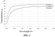
- Fig. 1 shows spectral curves of hole transport layers prepared using a doped nickel oxide target of Example 1 and a nickel oxide target of Comparative Example 1.
- Range disclosed in the present application is defined in the form of lower limits and upper limits, and with a given range being defined by selecting a lower limit and an upper limit, the selected lower and upper limits define boundaries of a specific range.
- a range defined in this manner may be inclusive or exclusive of end values, and may be arbitrarily combined, that is, any lower limit may be combined with any upper limit to form a range. For example, if ranges of 60 to 120 and 80 to 110 are listed for a particular parameter, it is understood that ranges of 60 to 110 and 80 to 120 are also expected.
- the numerical range "a-b" represents an abbreviated representation of any combination of real numbers between a and b, where both a and b are real numbers.
- the numerical range "0-5" means that all real numbers between "0-5" have been listed herein, and "0-5" is just an abbreviated representation of the combination of these numerical values.
- a certain parameter is an integer of ⁇ 2, it is equivalent to disclosing that the parameter is, for example, an integer of 2, 3, 4, 5, 6, 7, 8, 9, 10, 11, 12, etc.
- the method comprises steps (a) and (b), meaning that the method may comprise steps (a) and (b) performed sequentially, or may comprise steps (b) and (a) performed sequentially.
- the reference to the method may further comprise step (c), meaning that step (c) may be added to the method in any order, for example, the method may comprise steps (a), (b) and (c), or may comprise steps (a), (c) and (b), or may comprise steps (c), (a) and (b), and so on.
- the terms “comprise”, “comprising”, “include” and “including” mentioned in the present application may be open-ended or closed-ended.
- the “including” and “comprising” may indicate that it is possible to include or comprise other components not listed, and it is also possible to include or comprise only the listed components.
- the term "or” is inclusive in the present application.
- the phrase “A or B” means “A, B, or both A and B.” More specifically, the condition “A or B” is satisfied by any one of the following conditions: A is true (or present) and B is false (or absent); A is false (or absent) and B is true (or present); or both A and B are true (or present).
- the applicant found that in order to improve performance of the hole transport layer, it can be achieved by doping a nickel oxide thin-film as the hole transport layer with different elements.
- most of existing targets are single nickel oxide targets. If a doped nickel oxide thin-film is to be prepared, it is necessary to use a nickel oxide target and other targets to achieve by co-sputtering, in which the process is complicated, and doping elements in the obtained nickel oxide thin-film are also difficult to distribute uniformly, thereby limiting preparation of the doped nickel oxide thin-film and the improvement of electrical performances.
- the present application provides a doped nickel oxide target used to prepare the hole transport layer of the perovskite solar battery.
- the present application provides a doped nickel oxide target, which includes a nickel oxide substrate and a dopant doped therein, the dopant including at least one compound that contains one or more elements of Cu, Ca, Cr, Sn, Hg, Pb, Mg, Mn, Ag, Co, and Pr.
- the dopant includes at least one of CuO, CuzO, Cu 2 S, CuI, CuSCN, CuGaOz, CoO, Cr 2 O 3 , SnO, SnS, Hg 2 O, PbO, AgO, Ag 2 O, MnO, and Pr 2 O 3 .
- the above compounds are directly doped into the nickel oxide substrate as a dopant, the composition and content are more controllable than those in doping with a single substance, and electrical performances of the perovskite solar battery using the hole transport hole prepared by the target are further improved.
- the dopant includes at least two of CuO, CuzO, C U2 S, CuI, CuSCN, CuGaO 2 , CoO, Cr 2 O 3 , SnO, SnS, Hg 2 O, PbO, AgO, Ag 2 O, MnO, and Pr 2 O 3 .
- the inventor unexpectedly found that when at least two of the dopants are used for doping simultaneously, a prepared composite target contains various anions and cations of different valence states at the same time, so that a thin-film solar battery prepared therefrom has a larger regulation window of energy level structure, and is more convenient in energy level regulation, and photon conversion efficiency of the battery is further improved.
- the content of the dopant in the doped nickel oxide target is 0.1wt % to 20wt%.
- the content of CuO is 0 to 15%, the content of CuzO is 0 to 15%, the content of Cu 2 S is 0 to 15%, the content of CuI is 0 to 20%, the content of CuSCN is 0 to 15%, the content of CuGaOz is 0 to 15%, the content of CoO is 0 to 8%, the content of Cr 2 O 3 is 0 to 15%, the content of SnO is 0 to 15%, the content of SnS is 0 to 15%, the content of Hg 2 O is 0 to 15%, the content of PbO is 0 to 15%, the content of AgO is 0 to 15%, the content of Ag 2 O is 0 to 15%, the content of MnO is 0 to 10%, and the content of Pr 2 O 3 is 0 to 15%; and the total content of the dopant is 0.1% to 20%.
- the doped nickel oxide target is obtained by a classified plasma spraying method.
- the dopant is distributed inside the nickel oxide substrate more uniformly.
- the classified plasma spraying described in the present application can be understood as respectively and separately spraying different materials, for example, nickel oxide and one or more dopants.
- a second aspect of the present application provides a preparation method of a doped nickel oxide target, which includes: thermally spraying a coating for binding on a back panel or back tube of a target, respectively introducing nickel oxide powder and various dopant powders into their respective plasma generation sprayers, and respectively applying the nickel oxide and dopant onto the back panel or back tube of the target by plasma spraying simultaneously, to obtain the doped nickel oxide target, wherein the dopant is selected from at least one of compounds that contain one or more elements of Cu, Ca, Cr, Sn, Hg, Pb, Mg, Mn, Ag, Co, and Pr.
- the dopant is distributed more uniformly.
- the method of the present application can greatly increase a relative density of the target and reduce internal defects of the target, so that the obtained nickel oxide thin-film is more uniform, which is more conducive to the improvement of performance of the hole transport layer.
- the type and content of the dopant can be flexibly controlled, and a target doped with a suitable concentration and type of dopant can be directly prepared according to different performance requirements of the hole transport layer, so that the hole transport layer with the corresponding dopant type and content can be directly obtained through a sputtering process, thereby achieving convenience and accuracy of process adjustment.
- the preparation method provided by the present application has a simple process, strong controllability, and is convenient for rapid and efficient preparation and shaping in a wide range.
- the dopant is selected from at least one of CuO, CuzO, C U2 S, CuI, CuSCN, CuGaOz, CoO, Cr 2 O 3 , SnO, SnS, Hg 2 O, PbO, AgO, Ag 2 O, MnO, and Pr 2 O 3 .
- the dopant is selected from at least two of CuO, CuzO, C U2 S, CuI, CuSCN, CuGaO 2 , CoO, Cr 2 O 3 , SnO, SnS, Hg 2 O, PbO, AgO, Ag 2 O, MnO, and Pr 2 O 3 .
- the content of the dopant in the doped nickel oxide target is 0.1wt % to 20wt%.
- the content of CuO is 0 to 15%, the content of CuzO is 0 to 15%, the content of Cu 2 S is 0 to 15%, the content of CuI is 0 to 20%, the content of CuSCN is 0 to 15%, the content of CuGaO 2 is 0 to 15%, the content of CoO is 0 to 8%, the content of Cr 2 O 3 is 0 to 15%, the content of SnO is 0 to 15%, the content of SnS is 0 to 15%, the content of Hg 2 O is 0 to 15%, the content of PbO is 0 to 15%, the content of AgO is 0 to 15%, the content of Ag 2 O is 0 to 15%, the content of MnO is 0 to 10%, and the content of Pr 2 O 3 is 0 to 15%; and the total content of the dopant is 0.1% to 20%.
- a third aspect of the present application further provides use of the doped nickel oxide target provided in the first aspect of the present application or the doped nickel oxide target prepared by the method provided in the second aspect of the present application in preparation of a hole transport layer of a perovskite solar battery.
- a back panel was fixed to a holder of a plasma spraying device, and a layer of indium coating (binding material) for binding, with a thickness of 1.3 mm, was thermally sprayed on the back panel.
- a powdered nickel oxide substrate and a dopant AgO were respectively added to different plasma powder spraying material chambers of a powder plasma spraying box, so that different materials were separately added, respectively.
- the binding material of the back panel was heated at 200°C, and then plasmas of the dopant and nickel oxide substrate powder were sprayed onto the heated binding material through respective nozzles.
- Reference process parameter range was as follows: plasma power of 15KW, angle of 40°, and temperature of the back panel ranging from room temperature to 200°C. Deposition and mixing on the back panel were carried out by means of the nozzles forming an included-angle coverage to achieve a uniform doping effect. By controlling the spraying amount of the corresponding nozzle, the doping amount of AgO was controlled to be 0.5wt%.
- a doped nickel oxide material on the back panel was thickened continuously. After the thickness reached a set value of 16 mm, the spraying device stopped plasma spraying to obtain an AgO-doped nickel oxide target.
- step (2) except that the dopant in step (2) was adjust to CuI and the doping amount of CuI was controlled to be 20wt%, the rest were the same as in Example 1.
- step (2) the powdered nickel oxide substrate and dopants CuGaOzand SnS were respectively added to three different plasma powder spraying material chambers of the powder plasma spraying box, so that the different materials of the oxidized nickel substrate, CuGaOzand SnS were separately added, respectively; the doping amounts of CuGaOzand SnS were controlled to be 5wt% respectively; and the rest were the same as in Example 1.
- a spectral curve of the hole transport layer of the perovskite solar battery was measured by a Thermo Fisher Scientific iS 50 infrared spectrometer.
- Fig. 1 The spectral curves of the hole transport layers of perovskite solar batteries prepared from the targets of Example 1 and Comparative Example 1 are shown in Fig. 1 . It can be seen from Fig. 1 that the hole transport layer prepared using the doped nickel oxide target of the present application has higher transmittance for incident light of different wavelengths, indicating that the hole transport layer prepared using the doped nickel oxide target of the present application has a higher spectral response.
- Example 1 Number of samples CBM (eV) VBM (eV) ⁇ Eg (eV) Comparative Example 1 -1.31 -5.14 3.83 Example 1 -1.38 -5.20 3.82 Example 2 -1.44 -5.26 3.80 Example 3 -1.51 -5.30 3.79 Table 2 Number of samples Short-circuit current Isc(mA) Short-circuit current density Jsc(mA ⁇ cm -2 ) Voltage at open circuit Voc (V) Voltage at open circuit/battery (Voc/Cell) Fill factor(%) Photon-to-electron conversion efficiency(%) Area (cm 2 ) Example 1 114.10 21.39 12.33 1.03 69.24 15.22 64 113.65 21.31 12.64 1.05 68.69 15.42 64 Example 2 115.29 21.62 11.87 0.99 69.55 14.87 64 115.04 21.57 12.34 1.03 68.87 15.28 64 Example 3 114.40 21.45 12.09 1.01 72.01 15.
Landscapes
- Chemical & Material Sciences (AREA)
- Engineering & Computer Science (AREA)
- Materials Engineering (AREA)
- Physics & Mathematics (AREA)
- Metallurgy (AREA)
- Chemical Kinetics & Catalysis (AREA)
- Organic Chemistry (AREA)
- Mechanical Engineering (AREA)
- Plasma & Fusion (AREA)
- Analytical Chemistry (AREA)
- Power Engineering (AREA)
- Electromagnetism (AREA)
- Manufacturing & Machinery (AREA)
- Microelectronics & Electronic Packaging (AREA)
- Inorganic Compounds Of Heavy Metals (AREA)
- Compositions Of Oxide Ceramics (AREA)
- Photovoltaic Devices (AREA)
- Physical Vapour Deposition (AREA)
Abstract
Description
- The present application relates to the technical field of targets using a sputtering process, and in particular to, a doped nickel oxide target and a preparation method and application thereof.
- In perovskite solar batteries, efficient transport of photoinduced electrons depends on performance stability and repeatability of perovskite hole transport layers (HTL). At present, there are many materials that can be used as hole transport layers of perovskite thin-film batteries, among which nickel oxide is the most common. At present, a relatively mature technical means for preparing the hole transport layers is usually to prepare by a sputtering process using a nickel oxide target.
- With the continuous improvement of performance requirements for the perovskite solar batteries, how to improve performance of the hole transport layers is the focus of current research.
- The present application is made in view of the above problems, and an objective of the present application is to provide a novel doped nickel oxide target to improve performance of a hole transport layer prepared using the doped nickel oxide target.
- In order to achieve the above objective, the present application provides a doped nickel oxide target and a preparation method and application thereof.
- A first aspect of the present application provides a doped nickel oxide target, which includes a nickel oxide substrate and a dopant doped therein, the dopant including at least one of compounds that contain one or more elements of Cu, Ca, Cr, Sn, Hg, Pb, Mg, Mn, Ag, Co, and Pr.
- Therefore, in the present application, through doping with a specific compound, the hole transport layer of a perovskite solar battery prepared using the doped nickel oxide target of the present application has a narrower band gap and higher spectral response, and battery conversion efficiency is higher, indicating that performance of the perovskite solar battery and the hole transport layer prepared using the target of the present application is improved.
- In any of embodiments, the dopant includes at least one of CuO, CuzO, CU2S, CuI, CuSCN, CuGaOz, CoO, Cr2O3, SnO, SnS, Hg2O, PbO, AgO, Ag2O, MnO, and Pr2O3. The addition of the dopant is conductive to further improving performance of the hole transport layer and the battery.
- In any of embodiments, the dopant includes at least two of CuO, CuzO, Cu2S, CuI, CuSCN, CuGaO2, CoO, Cr2O3, SnO, SnS, Hg2O, PbO, AgO, Ag2O, MnO, and Pr2O3. The inventor unexpectedly found that performance of the battery, especially conversion efficiency thereof, is further improved when at least two of the dopants are used for doping simultaneously.
- In any of embodiments, the content of the dopant in the doped nickel oxide target is 0.1wt % to 20wt%.
- In any of embodiments, based on the total mass of the doped nickel oxide target, the content of CuO is 0 to 15%, the content of CuzO is 0 to 15%, the content of Cu2S is 0 to 15%, the content of CuI is 0 to 20%, the content of CuSCN is 0 to 15%, the content of CuGaO2 is 0 to 15%, the content of CoO is 0 to 8%, the content of Cr2O3 is 0 to 15%, the content of SnO is 0 to 15%, the content of SnS is 0 to 15%, the content of Hg2O is 0 to 15%, the content of PbO is 0 to 15%, the content of AgO is 0 to 15%, the content of Ag2O is 0 to 15%, the content of MnO is 0 to 10%, and the content of Pr2O3 is 0 to 15%; and the total content of the dopant is 0.1% to 20%.
- In any of embodiments, the doped nickel oxide target is obtained by a classified plasma spraying method. In the doped nickel oxide target obtained by the method, the dopant is distributed inside the nickel oxide substrate more uniformly.
- A second aspect of the present application provides a preparation method of a doped nickel oxide target, which includes:
thermally spraying a coating for binding on a back panel or back tube of a target, respectively introducing nickel oxide powder and various dopant powders into their respective plasma generation sprayers, and respectively applying the nickel oxide and dopant onto the back panel or back tube of the target by plasma spraying simultaneously, to obtain the doped nickel oxide target, wherein the dopant is selected from at least one of compounds that contain one or more elements of Cu, Ca, Cr, Sn, Hg, Pb, Mg, Mn, Ag, Co, and Pr. - By the method of the present application, the type and content of the dopant can be flexibly controlled, so that doped nickel oxide targets with different types and contents of dopants can be obtained. Further, the method of the present application is conductive to obtaining the doped nickel oxide target with dopant distributed more uniformly.
- A third aspect of the present application further provides use of the doped nickel oxide target provided in the first aspect of the present application or the doped nickel oxide target prepared by the method provided in the second aspect of the present application in preparation of a hole transport layer of a perovskite solar battery.
- The doped nickel oxide target provided in the present application includes one or more dopants, the hole transport layer of a perovskite solar battery prepared using the doped nickel oxide target of the present application has a narrower band gap and higher spectral response, and battery conversion efficiency is higher, indicating that battery performance can be improved by using the doped nickel oxide target to prepare the hole transport layer of a perovskite solar battery.
-
Fig. 1 shows spectral curves of hole transport layers prepared using a doped nickel oxide target of Example 1 and a nickel oxide target of Comparative Example 1. - Hereinafter, embodiments of a doped nickel oxide target and a preparation method and application thereof of the present application are described in detail and specifically disclosed with reference to the drawings as appropriate. However, there may be cases where unnecessary detailed description is omitted. For example, there are cases where detailed descriptions of well-known items and repeated descriptions of actually identical structures are omitted. This is to avoid unnecessary redundancy in the following descriptions and to facilitate the understanding by those skilled in the art. In addition, the drawings and subsequent descriptions are provided for those skilled in the art to fully understand the present application, and are not intended to limit the subject matter recited in the claims.
- "Range" disclosed in the present application is defined in the form of lower limits and upper limits, and with a given range being defined by selecting a lower limit and an upper limit, the selected lower and upper limits define boundaries of a specific range. A range defined in this manner may be inclusive or exclusive of end values, and may be arbitrarily combined, that is, any lower limit may be combined with any upper limit to form a range. For example, if ranges of 60 to 120 and 80 to 110 are listed for a particular parameter, it is understood that ranges of 60 to 110 and 80 to 120 are also expected. Additionally, if the
minimum range values 1 and 2 are listed, and if the maximum range values 3, 4, and 5 are listed, the following ranges are all contemplated: 1 to 3, 1 to 4, 1 to 5, 2 to 3, 2 to 4 and 2 to 5. In the present application, unless stated otherwise, the numerical range "a-b" represents an abbreviated representation of any combination of real numbers between a and b, where both a and b are real numbers. For example, the numerical range "0-5" means that all real numbers between "0-5" have been listed herein, and "0-5" is just an abbreviated representation of the combination of these numerical values. Additionally, when it is stated that a certain parameter is an integer of≥2, it is equivalent to disclosing that the parameter is, for example, an integer of 2, 3, 4, 5, 6, 7, 8, 9, 10, 11, 12, etc. - Unless otherwise specified, all embodiments and optional embodiments of the present application may be combined with each other to form new technical solutions.
- Unless otherwise specified, all technical features and optional technical features of the present application may be combined with each other to form new technical solutions.
- Unless otherwise specified, all steps of the present application may be performed sequentially or randomly, and preferably sequentially. For example, the method comprises steps (a) and (b), meaning that the method may comprise steps (a) and (b) performed sequentially, or may comprise steps (b) and (a) performed sequentially. For example, the reference to the method may further comprise step (c), meaning that step (c) may be added to the method in any order, for example, the method may comprise steps (a), (b) and (c), or may comprise steps (a), (c) and (b), or may comprise steps (c), (a) and (b), and so on.
- Unless otherwise specified, the terms "comprise", "comprising", "include" and "including" mentioned in the present application may be open-ended or closed-ended. For example, the "including" and "comprising" may indicate that it is possible to include or comprise other components not listed, and it is also possible to include or comprise only the listed components.
- Unless otherwise specified, the term "or" is inclusive in the present application. By way of example, the phrase "A or B" means "A, B, or both A and B." More specifically, the condition "A or B" is satisfied by any one of the following conditions: A is true (or present) and B is false (or absent); A is false (or absent) and B is true (or present); or both A and B are true (or present).
- In the process of studying a preparation process of a hole transport layer of a perovskite solar battery, the applicant found that in order to improve performance of the hole transport layer, it can be achieved by doping a nickel oxide thin-film as the hole transport layer with different elements. However, most of existing targets are single nickel oxide targets. If a doped nickel oxide thin-film is to be prepared, it is necessary to use a nickel oxide target and other targets to achieve by co-sputtering, in which the process is complicated, and doping elements in the obtained nickel oxide thin-film are also difficult to distribute uniformly, thereby limiting preparation of the doped nickel oxide thin-film and the improvement of electrical performances. In order to further improve performance of the hole transport layer to further improve performance of the perovskite solar battery, the present application provides a doped nickel oxide target used to prepare the hole transport layer of the perovskite solar battery.
- In an embodiment of the present application, the present application provides a doped nickel oxide target, which includes a nickel oxide substrate and a dopant doped therein, the dopant including at least one compound that contains one or more elements of Cu, Ca, Cr, Sn, Hg, Pb, Mg, Mn, Ag, Co, and Pr.
- Although the mechanism is not yet clear, the applicant unexpectedly found that when the doped nickel oxide target of the present application is used to prepare the hole transport layer of the perovskite solar battery, due to the compound doped with a specific element, the hole transport layer has a narrower band gap and higher spectral response, and battery conversion efficiency is significantly improved. Further, compared with co-sputtering and other methods, the method of using the doped nickel oxide target of the present application to prepare the hole transport layer can effectively improve a preparation process window of the doped hole transport layer, and is conductive to realizing process stability and consistency of thin films.
- In some embodiments, the dopant includes at least one of CuO, CuzO, Cu2S, CuI, CuSCN, CuGaOz, CoO, Cr2O3, SnO, SnS, Hg2O, PbO, AgO, Ag2O, MnO, and Pr2O3.
- The inventor found that when the dopant is a simple substance, because the simple substance and oxygen are prone to an incomplete reaction, the composition and doping ratio are not easy to control, and moreover, some simple substances such as Ga, Ag, Pb, I, and S are not easy to be powdered for plasma spraying. When the above compounds are directly doped into the nickel oxide substrate as a dopant, the composition and content are more controllable than those in doping with a single substance, and electrical performances of the perovskite solar battery using the hole transport hole prepared by the target are further improved.
- In some embodiments, the dopant includes at least two of CuO, CuzO, CU2S, CuI, CuSCN, CuGaO2, CoO, Cr2O3, SnO, SnS, Hg2O, PbO, AgO, Ag2O, MnO, and Pr2O3. The inventor unexpectedly found that when at least two of the dopants are used for doping simultaneously, a prepared composite target contains various anions and cations of different valence states at the same time, so that a thin-film solar battery prepared therefrom has a larger regulation window of energy level structure, and is more convenient in energy level regulation, and photon conversion efficiency of the battery is further improved.
- In some embodiments, the content of the dopant in the doped nickel oxide target is 0.1wt % to 20wt%. The inventor found that when the content of the dopant is within this range, it is conductive to improving performance of the prepared nickel oxide thin-film; if the content of the dopant is too much, for example, higher than 20wt%, performance of the nickel oxide substrate will be reduced, which is not conductive to the improvement of overall performance.
- In some embodiments, based on the total mass of the doped nickel oxide target, the content of CuO is 0 to 15%, the content of CuzO is 0 to 15%, the content of Cu2S is 0 to 15%, the content of CuI is 0 to 20%, the content of CuSCN is 0 to 15%, the content of CuGaOz is 0 to 15%, the content of CoO is 0 to 8%, the content of Cr2O3 is 0 to 15%, the content of SnO is 0 to 15%, the content of SnS is 0 to 15%, the content of Hg2O is 0 to 15%, the content of PbO is 0 to 15%, the content of AgO is 0 to 15%, the content of Ag2O is 0 to 15%, the content of MnO is 0 to 10%, and the content of Pr2O3 is 0 to 15%; and the total content of the dopant is 0.1% to 20%. The inventor found that different dopants have different optimal content ranges for improving performance of the hole transport layer, and when the above compounds are doped into the nickel oxide target in the concentration ranges described in the present application, it is more conductive to improving performance of the hole transport layer.
- In any of embodiments, the doped nickel oxide target is obtained by a classified plasma spraying method. In the doped nickel oxide target obtained by the method, the dopant is distributed inside the nickel oxide substrate more uniformly.
- The classified plasma spraying described in the present application can be understood as respectively and separately spraying different materials, for example, nickel oxide and one or more dopants.
- A second aspect of the present application provides a preparation method of a doped nickel oxide target, which includes:
thermally spraying a coating for binding on a back panel or back tube of a target, respectively introducing nickel oxide powder and various dopant powders into their respective plasma generation sprayers, and respectively applying the nickel oxide and dopant onto the back panel or back tube of the target by plasma spraying simultaneously, to obtain the doped nickel oxide target, wherein the dopant is selected from at least one of compounds that contain one or more elements of Cu, Ca, Cr, Sn, Hg, Pb, Mg, Mn, Ag, Co, and Pr. - In the doped nickel oxide target obtained by the method of the present application, the dopant is distributed more uniformly. In addition, the method of the present application can greatly increase a relative density of the target and reduce internal defects of the target, so that the obtained nickel oxide thin-film is more uniform, which is more conducive to the improvement of performance of the hole transport layer.
- In addition, by using the method of the present application, the type and content of the dopant can be flexibly controlled, and a target doped with a suitable concentration and type of dopant can be directly prepared according to different performance requirements of the hole transport layer, so that the hole transport layer with the corresponding dopant type and content can be directly obtained through a sputtering process, thereby achieving convenience and accuracy of process adjustment.
- Further, the preparation method provided by the present application has a simple process, strong controllability, and is convenient for rapid and efficient preparation and shaping in a wide range.
- In some embodiments, the dopant is selected from at least one of CuO, CuzO, CU2S, CuI, CuSCN, CuGaOz, CoO, Cr2O3, SnO, SnS, Hg2O, PbO, AgO, Ag2O, MnO, and Pr2O3.
- In some embodiments, the dopant is selected from at least two of CuO, CuzO, CU2S, CuI, CuSCN, CuGaO2, CoO, Cr2O3, SnO, SnS, Hg2O, PbO, AgO, Ag2O, MnO, and Pr2O3.
- In some embodiments, the content of the dopant in the doped nickel oxide target is 0.1wt % to 20wt%.
- In some embodiments, based on the total mass of the doped nickel oxide target, the content of CuO is 0 to 15%, the content of CuzO is 0 to 15%, the content of Cu2S is 0 to 15%, the content of CuI is 0 to 20%, the content of CuSCN is 0 to 15%, the content of CuGaO2 is 0 to 15%, the content of CoO is 0 to 8%, the content of Cr2O3 is 0 to 15%, the content of SnO is 0 to 15%, the content of SnS is 0 to 15%, the content of Hg2O is 0 to 15%, the content of PbO is 0 to 15%, the content of AgO is 0 to 15%, the content of Ag2O is 0 to 15%, the content of MnO is 0 to 10%, and the content of Pr2O3 is 0 to 15%; and the total content of the dopant is 0.1% to 20%.
- A third aspect of the present application further provides use of the doped nickel oxide target provided in the first aspect of the present application or the doped nickel oxide target prepared by the method provided in the second aspect of the present application in preparation of a hole transport layer of a perovskite solar battery.
- Examples of the present application will be described hereinafter. The examples described below are exemplary and only used to explain the present application, and should not be construed as a limitation on the present application. Where specific techniques or conditions are not specified in the examples, the techniques or conditions described in the literatures of the art or the product specifications are followed. Where manufacturers are not specified, the reagents or instruments used are conventional products and are commercially available.
- (1) A back panel was fixed to a holder of a plasma spraying device, and a layer of indium coating (binding material) for binding, with a thickness of 1.3 mm, was thermally sprayed on the back panel.
- (2) A powdered nickel oxide substrate and a dopant AgO were respectively added to different plasma powder spraying material chambers of a powder plasma spraying box, so that different materials were separately added, respectively.
- The binding material of the back panel was heated at 200°C, and then plasmas of the dopant and nickel oxide substrate powder were sprayed onto the heated binding material through respective nozzles. Reference process parameter range was as follows: plasma power of 15KW, angle of 40°, and temperature of the back panel ranging from room temperature to 200°C. Deposition and mixing on the back panel were carried out by means of the nozzles forming an included-angle coverage to achieve a uniform doping effect. By controlling the spraying amount of the corresponding nozzle, the doping amount of AgO was controlled to be 0.5wt%.
- With continuous performing of plasma spraying, a doped nickel oxide material on the back panel was thickened continuously. After the thickness reached a set value of 16 mm, the spraying device stopped plasma spraying to obtain an AgO-doped nickel oxide target.
- (3) The back panel of the target was removed to be subjected to laser cutting and trimming, the outer part of the edge the target was cut and recovered, and the edge was trimmed to form a target mounting edge, so that the basic secondary processing of the target was completed, and then the target was subjected to surface cleaning.
- Except that the doping amount of AgO was adjusted to 1wt%, the rest were the same as in Example 1.
- Except that the doping amount of AgO was adjusted to 2wt%, the rest were the same as in Example 1.
- Except that the dopant in step (2) was adjust to CuI and the doping amount of CuI was controlled to be 20wt%, the rest were the same as in Example 1.
- In addition to step (2), the powdered nickel oxide substrate and dopants CuGaOzand SnS were respectively added to three different plasma powder spraying material chambers of the powder plasma spraying box, so that the different materials of the oxidized nickel substrate, CuGaOzand SnS were separately added, respectively; the doping amounts of CuGaOzand SnS were controlled to be 5wt% respectively; and the rest were the same as in Example 1.
- Commercially available nickel oxide target.
-
- Step 1: An ITO conductive glass substrate was cleaned and dried by blowing, and then subjected to an ultraviolet light cleaning treatment to obtain a pretreated base substrate.
- Step 2: The pretreated base substrate and the doped nickel oxide targets of Examples 1 to 5 or the nickel oxide target of Comparative Example 1 were moved into a high-vacuum sputtering system, and a hole transport layer was sputtered on the pretreated base substrate. The specific conditions are as follows:
Oxygen was introduced as a working gas, a gas flow rate was 200 sccm; a sputtering pressure was 2.3×10⁻³mbar, a distance between the target and the base substrate was 79.5 mm, a sputtering power was 200 W, a heating temperature was 125°C, and a layer of doped nickel oxide thin-film with a thickness of 25 nm was deposited by sputtering as a hole transport layer. - Step 3: A perovskite precursor solution was spin-coated on the hole transport layer, then a chlorobenzene solvent was added to continue spin-coating, and annealing at 100°C was performed to obtain a perovskite crystal thin-film, that is, a light absorption layer.
- Step 4: A chlorobenzene solution of PCBM ([6,6]-phenyl-C61-isomethyl butyrate) was spin-coated on the light absorption layer to form an electron transport layer.
- Step 5: A metal electrode material silver-aluminum alloy was evaporated onto the electron transport layer by thermal evaporation under vacuum to obtain a perovskite solar battery.
- Energy band distribution of the hole transport layer of the perovskite solar battery was tested by an X-ray photoelectron spectrometer (XPS), model Escalab 250Xi (from Thermo Scientific), to obtain the valence band maximum (CBM value), conduction band minimum (VBM value), and energy band gap (ΔEg).
- A spectral curve of the hole transport layer of the perovskite solar battery was measured by a Thermo
Fisher Scientific iS 50 infrared spectrometer. - Energy band distribution results of the hole transport layers of perovskite solar batteries prepared using the doped nickel oxide targets prepared in Examples 1 to 3 and the nickel oxide target in Comparative Example 1 of the present application are shown in Table 1. Conversion efficiency results of the perovskite solar batteries prepared from the targets of various example and the comparative example are shown in Table 2.
- The spectral curves of the hole transport layers of perovskite solar batteries prepared from the targets of Example 1 and Comparative Example 1 are shown in
Fig. 1 . It can be seen fromFig. 1 that the hole transport layer prepared using the doped nickel oxide target of the present application has higher transmittance for incident light of different wavelengths, indicating that the hole transport layer prepared using the doped nickel oxide target of the present application has a higher spectral response.Table 1 Number of samples CBM (eV) VBM (eV) ΔEg (eV) Comparative Example 1 -1.31 -5.14 3.83 Example 1 -1.38 -5.20 3.82 Example 2 -1.44 -5.26 3.80 Example 3 -1.51 -5.30 3.79 Table 2 Number of samples Short-circuit current Isc(mA) Short-circuit current density Jsc(mA·cm-2) Voltage at open circuit Voc (V) Voltage at open circuit/battery (Voc/Cell) Fill factor(%) Photon-to-electron conversion efficiency(%) Area (cm2) Example 1 114.10 21.39 12.33 1.03 69.24 15.22 64 113.65 21.31 12.64 1.05 68.69 15.42 64 Example 2 115.29 21.62 11.87 0.99 69.55 14.87 64 115.04 21.57 12.34 1.03 68.87 15.28 64 Example 3 114.40 21.45 12.09 1.01 72.01 15.57 64 114.27 21.43 12.38 1.03 70.56 15.59 64 Example 4 114.45 21.46 12.04 1.00 71.96 15.49 64 114.35 21.44 12.33 1.03 70.78 15.59 64 Example 5 113.87 21.35 12.25 1.02 72.21 15.74 64 113.35 21.25 12.64 1.05 71.50 16.01 64 Comparative Example 1 90.81 17.03 12.07 1.01 72.52 12.42 64 90.63 16.99 12.44 1.04 71.32 12.57 64 - It can be seen from Table 1 that the hole transport layers prepared from the doped nickel oxide targets of Examples 1 to 3 have narrower energy band gap, indicating that the hole transport layer of the present application has a larger light absorption range.
- It can be seen from Table 2 that the short-circuit current and short-circuit current density as well as the photon-to-electron conversion efficiency of the battery using the hole transport layer prepared from the doped nickel oxide target of each example of the present application are significantly improved, and particularly, photon-to-electron conversion efficiency of a composite doped hole transport layer is further improved, indicating that electrical performances of the perovskite solar battery including the hole transport layer prepared using the doped nickel oxide target of the present application are significantly improved.
- The above descriptions are merely preferred examples of the present application, and are not intended to limit the present application. Any modifications, equivalent replacements, improvements, etc. made within the spirit and principle of the present application shall be included within the scope of protection of the present application.
Claims (12)
- A doped nickel oxide target, comprising a nickel oxide substrate and a dopant doped therein, the dopant comprising at least one of compounds that contain one or more elements of Cu, Ca, Cr, Sn, Hg, Pb, Mg, Mn, Ag, Co, and Pr.
- The doped nickel oxide target according to claim 1, wherein the dopant comprises at least one of CuO, Cu2O, Cu2S, CuI, CuSCN, CuGaO2, CoO, Cr2O3, SnO, SnS, Hg2O, PbO, AgO, Ag2O, MnO, and Pr2O3.
- The doped nickel oxide target according to claim 2, wherein the dopant comprises at least two of CuO, Cu2O, Cu2S, CuI, CuSCN, CuGaO2, CoO, Cr2O3, SnO, SnS, Hg2O, PbO, AgO, Ag2O, MnO, and Pr2O3.
- The doped nickel oxide target according to claim 1, wherein the content of the dopant in the doped nickel oxide target is 0. 1wt% to 20wt%.
- The doped nickel oxide target according to claim 2, wherein based on the total mass of the doped nickel oxide target, the content of CuO is 0 to 15%; the content of Cu2O is 0 to 15%; the content of Cu2S is 0 to 15%; the content of CuI is 0 to 20%; the content of CuSCN is 0 to 15%; the content of CuGaO2 is 0 to 15%; the content of CoO is 0 to 8%; the content of Cr2O3 is 0 to 15%; the content of SnO is 0 to 15%; the content of SnS is 0 to 15%; the content of Hg2O is 0 to 15%; the content of PbO is 0 to 15%; the content of AgO is 0 to 15%; the content of Ag2O is 0 to 15%; the content of MnO is 0 to 10%; and the content of Pr2O3 is 0 to 15%; and the total content of the dopant is 0.1% to 20%.
- The doped nickel oxide target according to any one of claims 1 to 5, being obtained by a classified plasma spraying method.
- A preparation method of a doped nickel oxide target, comprising:
thermally spraying a coating for binding on a back panel or back tube of a target, respectively introducing nickel oxide powder and various dopant powders into their respective plasma generation sprayers, and respectively applying the nickel oxide and dopant onto the back panel or back tube of the target by plasma spraying simultaneously, to obtain the doped nickel oxide target, wherein the dopant is selected from at least one of compounds that contain one or more elements of Cu, Ca, Cr, Sn, Hg, Pb, Mg, Mn, Ag, Co, and Pr. - The method according to claim 7, wherein the dopant is selected from at least one of CuO, Cu2O, Cu2S, CuI, CuSCN, CuGaO2, CoO, Cr2O3, SnO, SnS, Hg2O, PbO, AgO, Ag2O, MnO, and Pr2O3.
- The method according to claim 8, wherein the dopant is selected from at least two of CuO, Cu2O, Cu2S, CuI, CuSCN, CuGaO2, CoO, Cr2O3, SnO, SnS, Hg2O, PbO, AgO, Ag2O, MnO, and Pr2O3.
- The method according to claim 7, wherein the content of the dopant in the doped nickel oxide target is 0.1wt% to 20wt%.
- The method according to claim 8, wherein based on the total mass of the doped nickel oxide target, the content of CuO is 0 to 15%; the content of Cu2O is 0 to 15%; the content of Cu2S is 0 to 15%; the content of CuI is 0 to 20%; the content of CuSCN is 0 to 15%; the content of CuGaO2 is 0 to 15%; the content of CoO is 0 to 8%; the content of Cr2O3 is 0 to 15%; the content of SnO is 0 to 15%; the content of SnS is 0 to 15%; the content of Hg2O is 0 to 15%; the content of PbO is 0 to 15%; the content of AgO is 0 to 15%; the content of Ag2O is 0 to 15%; the content of MnO is 0 to 10%; and the content of Pr2O3 is 0 to 15%; and the total content of the dopant is 0.1% to 20%.
- Use of the doped nickel oxide target according to any one of claims 1 to 6 or the doped nickel oxide target prepared by the method according to any one of claims 7 to 11 in preparation of a hole transport layer of a perovskite solar battery.
Applications Claiming Priority (1)
| Application Number | Priority Date | Filing Date | Title |
|---|---|---|---|
| PCT/CN2021/134882 WO2023097583A1 (en) | 2021-12-01 | 2021-12-01 | Doped nickel oxide target material, and preparation method therefor and use thereof |
Publications (2)
| Publication Number | Publication Date |
|---|---|
| EP4227434A1 true EP4227434A1 (en) | 2023-08-16 |
| EP4227434A4 EP4227434A4 (en) | 2024-01-24 |
Family
ID=86611224
Family Applications (1)
| Application Number | Title | Priority Date | Filing Date |
|---|---|---|---|
| EP21962750.2A Pending EP4227434A4 (en) | 2021-12-01 | 2021-12-01 | DOPED NICKEL OXIDE TARGET MATERIAL, PREPARATION METHOD AND USE THEREOF |
Country Status (6)
| Country | Link |
|---|---|
| US (1) | US12595548B2 (en) |
| EP (1) | EP4227434A4 (en) |
| JP (1) | JP7765633B2 (en) |
| KR (1) | KR20240089692A (en) |
| CN (1) | CN118043493A (en) |
| WO (1) | WO2023097583A1 (en) |
Families Citing this family (2)
| Publication number | Priority date | Publication date | Assignee | Title |
|---|---|---|---|---|
| CN118206360B (en) * | 2024-03-21 | 2026-01-02 | 洛阳晶联光电材料有限责任公司 | A high-density nickel oxide-based rotating target and its preparation method |
| CN119191819A (en) * | 2024-10-08 | 2024-12-27 | 江苏迪丞光电材料有限公司 | Method and device for preparing nickel oxide-doped oxide target for perovskite |
Family Cites Families (20)
| Publication number | Priority date | Publication date | Assignee | Title |
|---|---|---|---|---|
| US5427993A (en) * | 1993-08-30 | 1995-06-27 | Regents, The University Of California | Process for forming a homogeneous oxide solid phase of catalytically active material |
| GB9600210D0 (en) * | 1996-01-05 | 1996-03-06 | Vanderstraeten E Bvba | Improved sputtering targets and method for the preparation thereof |
| WO2003014254A1 (en) * | 2001-08-07 | 2003-02-20 | Midwest Research Institute | Electrochromic counter electrode |
| FR2835534B1 (en) * | 2002-02-06 | 2004-12-24 | Saint Gobain | NON STOECHIOMETRIC CERAMIC TARGET NiOx |
| EP3360855B1 (en) * | 2006-05-18 | 2020-03-18 | Hydro-Quebec | Method for preparing ceramics, ceramics thus obtained and uses thereof, particularly as a target for cathode sputtering |
| FR2944293B1 (en) * | 2009-04-10 | 2012-05-18 | Saint Gobain Coating Solutions | THERMAL PROJECTION DEVELOPING METHOD OF A TARGET |
| JP2013507526A (en) * | 2009-10-15 | 2013-03-04 | ユミコア エセ.アー. | Tin oxide ceramic sputtering target and method for producing the same |
| DE102010047756B3 (en) * | 2010-10-08 | 2012-03-01 | Heraeus Materials Technology Gmbh & Co. Kg | Sputtering target, useful for sputter deposition, comprises a mixture of oxides of indium, zinc and gallium and a ternary mixed oxide of indium, zinc and gallium |
| JP5996227B2 (en) * | 2012-03-26 | 2016-09-21 | 学校法人 龍谷大学 | Oxide film and manufacturing method thereof |
| CN104451582B (en) | 2014-12-30 | 2017-09-29 | 北京恒隆科技有限公司 | A kind of electric conductive oxidation zirconium rotary target material and preparation method thereof |
| CN105322026B (en) * | 2015-09-30 | 2018-08-24 | 天津职业技术师范大学 | A kind of NiO:Ag/TiOx diode of heterogenous pn junction |
| CN108063186A (en) | 2017-11-20 | 2018-05-22 | 济南大学 | Zinc doping nickel oxide hole transmission layer inverts perovskite solar cell and preparation method |
| KR20200017847A (en) | 2018-08-09 | 2020-02-19 | 고려대학교 산학협력단 | Method of manufacturing piezoelectric thin film and piezoelectric sensor using piezoelectric thin film |
| GB201819380D0 (en) * | 2018-11-28 | 2019-01-09 | Univ Oxford Innovation Ltd | Long-term stable optoelectronic device |
| CN112441819A (en) * | 2020-11-13 | 2021-03-05 | 北京航大微纳科技有限公司 | Hot isostatic pressing preparation method of nickel oxide-based ceramic target material |
| CN112456971A (en) * | 2020-11-13 | 2021-03-09 | 北京航大微纳科技有限公司 | Cold isostatic pressing preparation method of nickel oxide-based ceramic target material |
| CN112624739A (en) * | 2020-11-13 | 2021-04-09 | 北京航空航天大学宁波创新研究院 | Nickel oxide-based ceramic target material, thin film and thin film preparation process |
| CN112321280A (en) * | 2020-11-13 | 2021-02-05 | 北京航大微纳科技有限公司 | Gel injection molding preparation method of nickel oxide-based ceramic target material |
| CN112374554A (en) * | 2020-11-13 | 2021-02-19 | 北京航大微纳科技有限公司 | High-purity high-activity nickel oxide-based powder, preparation method and application |
| CN112481592A (en) * | 2020-11-13 | 2021-03-12 | 北京航大微纳科技有限公司 | Hot press molding preparation method of nickel oxide-based ceramic target material |
-
2021
- 2021-12-01 KR KR1020247015875A patent/KR20240089692A/en active Pending
- 2021-12-01 EP EP21962750.2A patent/EP4227434A4/en active Pending
- 2021-12-01 WO PCT/CN2021/134882 patent/WO2023097583A1/en not_active Ceased
- 2021-12-01 CN CN202180102993.1A patent/CN118043493A/en active Pending
- 2021-12-01 JP JP2024528480A patent/JP7765633B2/en active Active
-
2023
- 2023-03-30 US US18/193,382 patent/US12595548B2/en active Active
Also Published As
| Publication number | Publication date |
|---|---|
| EP4227434A4 (en) | 2024-01-24 |
| JP7765633B2 (en) | 2025-11-06 |
| US20230235448A1 (en) | 2023-07-27 |
| WO2023097583A1 (en) | 2023-06-08 |
| CN118043493A (en) | 2024-05-14 |
| KR20240089692A (en) | 2024-06-20 |
| US12595548B2 (en) | 2026-04-07 |
| JP2024545593A (en) | 2024-12-10 |
Similar Documents
| Publication | Publication Date | Title |
|---|---|---|
| US12595548B2 (en) | Doped nickel oxide target and preparation method and application thereof | |
| EP2539942B1 (en) | Process and apparatus for fabrication of a semiconductor layer | |
| Eze et al. | Optimum silver contact sputtering parameters for efficient perovskite solar cell fabrication | |
| WO2009135114A2 (en) | Transparent conductive materials including cadmium stannate | |
| JPH07326783A (en) | Formation of photovoltatic element and thin film manufacturing device used therefor | |
| EP4228011A1 (en) | Method for forming hole transport layer on surface of substrate, and hole transport layer, solar cell and preparation method therefor, and photovoltaic module | |
| CN102437206B (en) | ZnO/CdSe/CdTe nanorod array photoelectrode and preparation method thereof | |
| DE102011056639A1 (en) | Method for producing a transparent conductive oxide layer and a photovoltaic device | |
| WO2022071302A1 (en) | Perovskite thin film solar cell production method | |
| CN113707817A (en) | Preparation method of inorganic hole transport layer of perovskite solar cell | |
| US20250386616A1 (en) | Solar cell preparation method, and coating carrier plate for solar cell and application thereof | |
| JP4377003B2 (en) | Method for adjusting sheet resistance value of transparent conductive film and method for forming transparent conductive film | |
| JP2009021607A (en) | Method for producing transparent conductive oxide coating | |
| CN101838794A (en) | Method for preparing titania film by using gas flow reaction sputtering under middle gas pressure and method for preparing solar cell | |
| JPH11195801A (en) | Photovoltaic element | |
| JP4397451B2 (en) | Transparent conductive thin film and method for producing the same | |
| EP4546435A1 (en) | Tco coating method, tco coating device, and solar cell and preparation method therefor | |
| CN115224199B (en) | Perovskite solar cells and their fabrication methods | |
| KR102441941B1 (en) | Metal oxide device, preparation method thereof, and photoelectric device comprising same | |
| JP2000004036A (en) | Method for forming microcrystalline semiconductor layer and photovoltaic element | |
| JP2726323B2 (en) | Thin-film solar cell fabrication method | |
| KR102721758B1 (en) | Method for manufacturing perovskite thin film, and perovskite thin film and solar cell related thereto | |
| CN110931640A (en) | Perovskite solar cell and preparation method thereof | |
| Abolmasov et al. | Influence of DC-sputtered ITO layers on performance of silicon heterojunction solar cells | |
| CN118678852A (en) | Solar cell and preparation method thereof |
Legal Events
| Date | Code | Title | Description |
|---|---|---|---|
| STAA | Information on the status of an ep patent application or granted ep patent |
Free format text: STATUS: UNKNOWN |
|
| STAA | Information on the status of an ep patent application or granted ep patent |
Free format text: STATUS: THE INTERNATIONAL PUBLICATION HAS BEEN MADE |
|
| PUAI | Public reference made under article 153(3) epc to a published international application that has entered the european phase |
Free format text: ORIGINAL CODE: 0009012 |
|
| STAA | Information on the status of an ep patent application or granted ep patent |
Free format text: STATUS: REQUEST FOR EXAMINATION WAS MADE |
|
| 17P | Request for examination filed |
Effective date: 20230508 |
|
| AK | Designated contracting states |
Kind code of ref document: A1 Designated state(s): AL AT BE BG CH CY CZ DE DK EE ES FI FR GB GR HR HU IE IS IT LI LT LU LV MC MK MT NL NO PL PT RO RS SE SI SK SM TR |
|
| REG | Reference to a national code |
Ref country code: DE Ref legal event code: R079 Free format text: PREVIOUS MAIN CLASS: C23C0014350000 Ipc: C23C0014340000 |
|
| A4 | Supplementary search report drawn up and despatched |
Effective date: 20240103 |
|
| RIC1 | Information provided on ipc code assigned before grant |
Ipc: H10K 85/50 20230101ALN20231220BHEP Ipc: H10K 30/86 20230101ALN20231220BHEP Ipc: H10K 30/40 20230101ALN20231220BHEP Ipc: H10K 71/30 20230101ALI20231220BHEP Ipc: H01J 37/34 20060101ALI20231220BHEP Ipc: C23C 4/134 20160101ALI20231220BHEP Ipc: C23C 4/10 20160101ALI20231220BHEP Ipc: C23C 14/34 20060101AFI20231220BHEP |
|
| RAP1 | Party data changed (applicant data changed or rights of an application transferred) |
Owner name: CONTEMPORARY AMPEREX TECHNOLOGY(HONG KONG) LIMITED |
|
| DAV | Request for validation of the european patent (deleted) | ||
| DAX | Request for extension of the european patent (deleted) |