EP4224825A1 - Support, module assembly, and electronic device - Google Patents
Support, module assembly, and electronic device Download PDFInfo
- Publication number
- EP4224825A1 EP4224825A1 EP22868417.1A EP22868417A EP4224825A1 EP 4224825 A1 EP4224825 A1 EP 4224825A1 EP 22868417 A EP22868417 A EP 22868417A EP 4224825 A1 EP4224825 A1 EP 4224825A1
- Authority
- EP
- European Patent Office
- Prior art keywords
- module
- bracket
- limiting
- electronic device
- connecting end
- Prior art date
- Legal status (The legal status is an assumption and is not a legal conclusion. Google has not performed a legal analysis and makes no representation as to the accuracy of the status listed.)
- Granted
Links
Images








Classifications
-
- H—ELECTRICITY
- H04—ELECTRIC COMMUNICATION TECHNIQUE
- H04M—TELEPHONIC COMMUNICATION
- H04M1/00—Substation equipment, e.g. for use by subscribers
- H04M1/02—Constructional features of telephone sets
- H04M1/0202—Portable telephone sets, e.g. cordless phones, mobile phones or bar type handsets
- H04M1/026—Details of the structure or mounting of specific components
-
- G—PHYSICS
- G06—COMPUTING OR CALCULATING; COUNTING
- G06F—ELECTRIC DIGITAL DATA PROCESSING
- G06F1/00—Details not covered by groups G06F3/00 - G06F13/00 and G06F21/00
- G06F1/16—Constructional details or arrangements
- G06F1/1613—Constructional details or arrangements for portable computers
- G06F1/1633—Constructional details or arrangements of portable computers not specific to the type of enclosures covered by groups G06F1/1615 - G06F1/1626
- G06F1/1656—Details related to functional adaptations of the enclosure, e.g. to provide protection against EMI, shock, water, or to host detachable peripherals like a mouse or removable expansions units like PCMCIA cards, or to provide access to internal components for maintenance or to removable storage supports like CDs or DVDs, or to mechanically mount accessories
- G06F1/1658—Details related to functional adaptations of the enclosure, e.g. to provide protection against EMI, shock, water, or to host detachable peripherals like a mouse or removable expansions units like PCMCIA cards, or to provide access to internal components for maintenance or to removable storage supports like CDs or DVDs, or to mechanically mount accessories related to the mounting of internal components, e.g. disc drive or any other functional module
-
- G—PHYSICS
- G06—COMPUTING OR CALCULATING; COUNTING
- G06F—ELECTRIC DIGITAL DATA PROCESSING
- G06F1/00—Details not covered by groups G06F3/00 - G06F13/00 and G06F21/00
- G06F1/16—Constructional details or arrangements
- G06F1/1613—Constructional details or arrangements for portable computers
- G06F1/1633—Constructional details or arrangements of portable computers not specific to the type of enclosures covered by groups G06F1/1615 - G06F1/1626
- G06F1/1684—Constructional details or arrangements related to integrated I/O peripherals not covered by groups G06F1/1635 - G06F1/1675
- G06F1/1698—Constructional details or arrangements related to integrated I/O peripherals not covered by groups G06F1/1635 - G06F1/1675 the I/O peripheral being a sending/receiving arrangement to establish a cordless communication link, e.g. radio or infrared link, integrated cellular phone
-
- G—PHYSICS
- G06—COMPUTING OR CALCULATING; COUNTING
- G06F—ELECTRIC DIGITAL DATA PROCESSING
- G06F1/00—Details not covered by groups G06F3/00 - G06F13/00 and G06F21/00
- G06F1/16—Constructional details or arrangements
- G06F1/20—Cooling means
- G06F1/203—Cooling means for portable computers, e.g. for laptops
-
- H—ELECTRICITY
- H01—ELECTRIC ELEMENTS
- H01Q—ANTENNAS, i.e. RADIO AERIALS
- H01Q1/00—Details of, or arrangements associated with, antennas
- H01Q1/12—Supports; Mounting means
-
- H—ELECTRICITY
- H01—ELECTRIC ELEMENTS
- H01Q—ANTENNAS, i.e. RADIO AERIALS
- H01Q1/00—Details of, or arrangements associated with, antennas
- H01Q1/12—Supports; Mounting means
- H01Q1/22—Supports; Mounting means by structural association with other equipment or articles
- H01Q1/24—Supports; Mounting means by structural association with other equipment or articles with receiving set
- H01Q1/241—Supports; Mounting means by structural association with other equipment or articles with receiving set used in mobile communications, e.g. GSM
- H01Q1/242—Supports; Mounting means by structural association with other equipment or articles with receiving set used in mobile communications, e.g. GSM specially adapted for hand-held use
- H01Q1/243—Supports; Mounting means by structural association with other equipment or articles with receiving set used in mobile communications, e.g. GSM specially adapted for hand-held use with built-in antennas
-
- H—ELECTRICITY
- H05—ELECTRIC TECHNIQUES NOT OTHERWISE PROVIDED FOR
- H05K—PRINTED CIRCUITS; CASINGS OR CONSTRUCTIONAL DETAILS OF ELECTRIC APPARATUS; MANUFACTURE OF ASSEMBLAGES OF ELECTRICAL COMPONENTS
- H05K7/00—Constructional details common to different types of electric apparatus
- H05K7/20—Modifications to facilitate cooling, ventilating, or heating
- H05K7/2039—Modifications to facilitate cooling, ventilating, or heating characterised by the heat transfer by conduction from the heat generating element to a dissipating body
Definitions
- This application relates to the field of electronic technologies, and in particular, to a bracket, a module assembly, and an electronic device.
- a millimeter wave module may be incorporated into electronic products such as mobile phones.
- the main function of such a module is to realize signal transmission in a millimeter wave band.
- Current millimeter wave modules are usually packaged devices, including a circuit board, a chip, an antenna module, and a BTB (Board to Board) connector, which are configured to connect to a circuit board in the mobile phone. After the millimeter wave module is mounted in the mobile phone, position stability and connection stability need to be maintained.
- BTB Board to Board
- Embodiments of this application provide a bracket, a module assembly, and an electronic device, which may mount a module more stably, to improve position stability of the module in the electronic device.
- an embodiment of this application provides a bracket for a module, two first limiting parts arranged opposite to each other are arranged at two ends of the bracket, a second limiting part is arranged on at least one side of the bracket, and the two first limiting parts and the second limiting part are enclosed to form a mounting position for mounting the module.
- Two first limiting parts at two ends and a second limiting part at least at one side are enclosed to form a mounting position, and both the first limiting parts and the second limiting part may limit the module, so as to limit in all directions and ensure position stability of the module in the bracket.
- the bracket is further fixed to the electronic device through fixing parts, so that the position stability of the module in the electronic device may be ensured.
- an embodiment of this application further provides a first implementation according to the aspect.
- the bracket includes a bottom plate and vertical plates at two ends of the bottom plate, and the vertical plates form the first limiting parts; and a first flange is arranged on only one side of the bottom plate, and the first flange forms the second limiting part.
- a bottom plate is further arranged while two first limiting parts and one second limiting part are arranged, and the bottom plate may provide a better supporting role for the module, to further ensure mounting on the module in a limited manner.
- an embodiment of this application further provides a second implementation according to the aspect.
- a second flange opposite to an extension direction of the first flange is arranged on the other side of the bottom plate, and the second flange is configured to bond a circuit board element and/or an electronic device.
- the second flange may bond the circuit board element and the electronic device, thereby facilitating fixing of the circuit board element and improving reliability of connection between the bracket and the electronic device.
- an embodiment of this application further provides a third implementation according to the aspect.
- the bracket is made of copper alloy or carbon fiber. Copper alloy and carbon fiber have high strength, meet strength requirements, and have good heat dissipation performance, which is also beneficial to heat dissipation of the module in a case that heat dissipation is required, thereby improving user experience.
- an embodiment of this application further provides a fourth implementation according to the aspect.
- the bracket includes two side plates arranged opposite to each other and two end plates arranged opposite to each other, the end plate is the first limiting part, and the side plate is the second limiting part; and the two side plates and the two end plates are enclosed to form the mounting position, and an inner wall of at least one of the side plate or the end plate is at least partially provided with an elastic part made of an elastic material in a protruding manner, so as to be in an interference fit with the module.
- the bracket is enclosed by two first limiting parts and two second limiting parts to form a mounting position, to limit the module more comprehensively in a circumferential direction, and limit is realized by interference pressing of the elastic part, so that limit is reliable and may not damage the module.
- the bottom of the bracket may also be empty by performing interference pressing, so that it is more convenient to mount the module, and the module assembly is not easy to float after mounting.
- an embodiment of this application further provides a fifth implementation according to the aspect.
- the end plate and the side plate are integrally formed through injection molding, the elastic part is made of soft plastic, and other parts of the end plate and the side plate are made of hard plastic.
- Integrated injection molding is beneficial to ensuring integration of the bracket, and the elastic part is not prone to be separated from other parts.
- the soft plastic is beneficial to realizing interference pressing, and the hard plastic part is beneficial to ensuring the strength of the bracket.
- the plastic material has no or little influence on the function of the module.
- an embodiment of this application further provides a sixth implementation according to the aspect.
- the module includes an external connecting end, and the bracket is provided with a notch to expose the external connecting end.
- the notch is arranged to expose the external connecting end, so as to facilitate connection between the external connecting end and the external components, and avoid scratching the external connecting end or connected external components.
- an embodiment of this application further provides a seventh implementation according to the aspect.
- the bracket is separately arranged on the electronic device, and the bracket includes fixing parts, where the fixing parts are configured to fix the bracket to the electronic device; or the bracket is integrally formed on a housing of the electronic device.
- the bracket is integrally arranged on the housing of the electronic device, and there is no need to perform a fixing operation.
- the bracket is separately arranged in the electronic device, which is convenient to process.
- an embodiment of this application further provides an eighth implementation according to the aspect.
- the bracket is separately arranged on the electronic device, the fixing parts are fixed or integrally arranged on the first limiting parts, and the fixing parts are provided with connecting holes configured for fixing to the electronic device.
- the fixing part is arranged on the first limiting part, that is, at two ends of the bracket, and connecting holes are provided, thereby facilitating implementation of a fastening operation.
- an embodiment of this application further provides a module assembly, including a module and a bracket for mounting the module.
- the bracket is a bracket according to an aspect and the first implementation to the eighth implementation of the aspect, and the module is mounted at the mounting position of the bracket.
- the module assembly has the same technical effect as the bracket.
- an embodiment of this application further provides a first implementation according to the second aspect.
- the module includes an external connecting end
- the module assembly further includes a connection structure
- the connection structure includes a main body portion and a first connecting end and a second connecting end that are arranged on the main body portion, the first connecting end is configured to be connected to the external connecting end of the module 1, and the second connecting end is configured to connect an electronic element of the electronic device; and the main body portion is capable of being fixed to the second limiting part.
- the main body portion of the connection structure is fixed to the second limiting part, so that connection between the first connecting end and the second connecting end does not interfere with each other, and the connection reliability is higher.
- an embodiment of this application further provides a second implementation according to the second aspect.
- the main body portion is bonded to the second limiting part.
- Such a bonding manner is simple and may not damage the connection structure.
- an embodiment of this application further provides a third implementation according to the second aspect.
- At least one of a heat conductive pad or a circuit board element is fixed on the bottom of the module assembly.
- the heat conductive pad is arranged on the bottom of the module assembly, which can effectively improve the heat dissipation effect of the module assembly and improve the user experience.
- the heat conductive pad is arranged on the bottom of the module assembly, which may not be damaged during the mounting, thereby maintain the heat conduction performance.
- an embodiment of this application further provides a fourth implementation according to the second aspect.
- a limiting structure is arranged on the bottom of the bracket, and the limiting structure prevents the circuit board element from being separated from the bottom.
- the circuit board element is limited by the limiting structure, which is beneficial to ensuring the position stability of the circuit board element in the electronic device.
- an embodiment of this application further provides a fifth implementation according to the second aspect.
- the limiting structure is a protrusion or concave part arranged on the bottom of the bracket, and the circuit board element includes a corresponding concave part or protrusion; or the limiting structure is a concave part arranged on the bottom of the bracket, and the circuit board element is capable of being embedded into the concave part.
- the limit is simple based on convex-concave coordination, and it is easy to realize limit and process the structure.
- an embodiment of this application further provides a sixth implementation according to the second aspect.
- a bottom plate is arranged on the bottom of the bracket, and the bottom of the module is bonded to the bottom plate.
- the module is bonded to the bottom plate, which may further improve the position stability of the module in the bracket.
- an embodiment of this application further provides a seventh implementation according to the second aspect.
- the module is bonded to at least one of the first limiting part or the second limiting part.
- the module is connected to the first limiting parts and the second limiting part, which may further improve the position stability of the module in the bracket.
- an embodiment of this application further provides an eighth implementation according to the second aspect.
- the module includes a chip, where the chip is bonded to the second limiting part.
- the chip may have a heat generating component bonded to the second limiting part, to accelerate heat dissipation.
- an embodiment of this application further provides a ninth implementation according to the second aspect.
- the module includes an antenna module capable of performing communication, the second limiting part is arranged on only one side of the bracket, the other side of the bracket is provided with an opening, and the antenna module faces the opening.
- the antenna module faces the opening, that is, the opening is in an external radiation region of the antenna module, so that the communication function of the antenna module may not be affected.
- an embodiment of this application further provides a tenth implementation according to the second aspect.
- the module is a millimeter wave module.
- the millimeter wave module may transmit signals in a millimeter wave band.
- the millimeter wave module can be stably arranged in the electronic device to stably transmit signals.
- an embodiment of this application further provides an electronic device including the module assembly according to the second aspect and any one of the first to tenth implementations of the second aspect.
- the electronic device has the same technical effect as the module assembly.
- an embodiment of this application further provides a first implementation according to the third aspect.
- the electronic device is a mobile phone
- the module assembly is arranged in a middle frame of the mobile phone.
- the module assembly is arranged in the middle frame, which can be fixed through the middle frame and is convenient to mount.
- an embodiment of this application further provides a second implementation according to the third aspect.
- a heat conductive pad is arranged between the bottom of the module assembly and a bottom wall of the middle frame.
- the heat conductive pad may guide heat of the module to the bottom wall of the middle frame as soon as possible, so as to achieve the purpose of dissipating heat to the outside.
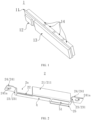
- FIG. 1 is a schematic diagram of a module 1 according to Embodiment 1 of this application.
- the module 1 in this embodiment of this application is specifically a millimeter wave module and is mainly configured to achieve signal transmission in a millimeter wave band.
- the millimeter wave module includes a circuit board 11, a plurality of antenna modules 14 arranged on one side of the circuit board 11 configured to realize communication, a chip 13 arranged on the other side of the circuit board 11, and an external connecting end 12.
- the external connecting end 12 is, for example, a BTB connector, and the external connecting end 12 may connect the millimeter wave module to a circuit board element of a mobile phone, for example, to a main board 200 of the mobile phone.
- the module 1 may be mounted in a bracket 2, and the two are assembled into a module assembly.
- the module assembly is mounted into the electronic device.
- the module assembly in this embodiment of this application is specifically mounted in a middle frame 100 of the mobile phone, which may be understood with reference to FIG. 2 to FIG. 6 .
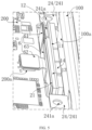
- FIG. 2 is a schematic structural diagram of arranging a heat conductive pad 4 and a back adhesive 51 on the bracket 2 according to Embodiment 1.
- FIG. 3 is a schematic structural diagram of a bracket 2 in FIG. 2 from another perspective.
- FIG. 4 is a schematic diagram of a module assembly formed by mounting the module 1 in FIG. 1 on the bracket 2 in FIG. 2 .
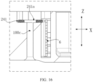
- FIG. 5 is a schematic diagram of the module assembly in FIG. 4 arranged in a middle frame 100 of a mobile phone.
- FIG. 6 is a top view of FIG. 5 .
- the bracket 2 includes a bottom plate 22 and vertical plates 231 located at two ends of the bottom plate 22.
- the vertical plates 231 form the first limiting parts 23.
- a first flange 211 is arranged on only one side of the bottom plate 22, and the first flange 211 forms the second limiting part 21.
- the module 1 is arranged on the bottom plate 22, and one side of the module 1 is limited by the first flange 211 that is used as the second limiting part 21. As shown in FIG. 4 , one side on which a chip 13 is arranged in the module 1 is limited by the first flange 211, and two ends of the module 1 are limited by the vertical plates 231 that are used as the first limiting parts 23.
- the bracket 2 further includes fixing parts 24, where the fixing parts 24 are configured to fix the bracket 2 to the middle frame 100 of the mobile phone.
- edges of the vertical plates 231 far away from the bottom plate 22 extend in directions far away from the mounting position to form fixing flanges 241, and the fixing flanges 241 are used as the fixing parts 24.
- Connecting holes 241a are provided on the fixing flanges 241, and the bracket 2 may be fixed to the middle frame 100 of the mobile phone by inserting screws into the corresponding connecting holes 241a.
- the fixing part 24 may also be arranged on another position of the bracket 2, for example, may be separately fixed to the bottom or a side edge of the bracket 2, which is mainly designed according to a mounting position of the module assembly in the mobile phone, to facilitate fastening.
- the fixing flanges 241, the vertical plates 231, the bottom plate 22, and the first flange 211 are all integrally formed, which have better strength and are easy to process.
- the bracket 2 may be first fixed in the middle frame 100, and then the module 1 is mounted, or the bracket 2 and the module 1 may be assembled into the module assembly, and then the assembly may be integrally mounted in the middle frame 100.
- Two first limiting parts 23 and one second limiting part 21 of the bracket 2 need to have a certain limiting effect on the module 1, to maintain the position stability of the module 1 on the bracket 2.
- a distance between the two first limiting parts 23, that is, a length of the bottom plate 22 is slightly longer than a length of the module 1.
- a gap may be 0.1 mm
- the module 1 is mounted to the bracket 2 in a top-edge alignment manner, that is, the two ends of the module 1 and the first limiting parts 23 are zero-matched, and then the module 1 is fixed to the second limiting part 21 by using a back adhesive, so that it is convenient for mounting without damaging the module 1, and limiting is achieved.
- the bracket 2 is made of copper alloy (such as C1940 alloy), a carbon fiber, or other materials with certain strength, and such material may have better heat dissipation performance, to facilitate the module 1 in heat dissipation.
- the material of the bracket 2 is not limited as long as it meets strength requirements of mounting and protecting the module 1, and it is better to consider certain heat dissipation performance.
- a length of the first flange 211 of the bracket 2 is less than a length of a corresponding side of the bottom plate 22, that is, the first flange 211 is not arranged on one side of the bottom plate 22 in an entire length direction.
- the first flange 211 since the length of the first flange 211 is less than the length of one side of the bottom plate 22, the first flange 211 is connected to a vertical plate 231 at an end of the bottom plate 22, and there is a gap therebetween.
- the gap may be defined as a first notch 2a.
- the first notch 2a corresponds to an external connecting end 12 of the module 1, so that the external connecting end 12 establishes a connection to an external element at a position of the first notch 2a.
- a position is reserved to avoid the external connecting end 12, to prevent the bracket 2 from interfering with connection of the external connecting end 12 and scratching the external connecting end 12.
- the first notch 2a is reserved between one end of the first flange 211 and a vertical plate 231 at one end of the bottom plate 22, and the other end of the first flange 211 and a vertical plate 231 at the other end of the bottom plate 22 may have a relatively small gap therebetween or may be connected to each other.
- the length of the first flange 211 may be as long as possible, to improve a capability of limiting the module 1.
- the length of the first flange 211 may be exceed half of the length of the module 1, where the length of the module 1 is a size of the module 1 in an arrangement direction of a plurality of antenna modules 14 in FIG. 1 .
- the length of the module 1 is basically the same as the length of the bottom plate 22, to achieve zero matching with the vertical plates 231 at two ends as much as possible.
- the length of the module 1 is slightly less than the length of the bottom plate 22. In this way, smooth assembly and a limiting effect of the vertical plates 231 at two ends after assembly may be ensured. Therefore, the length of the first flange 211 exceeds half of the length of the bottom plate 22 in this case.
- the first notch 2a is not limited to be provided between the first flange 211 and one vertical plate 231, which may be designed according to a position of the external connecting end 12 on the module 1.
- the first flange 211 may reserve a corresponding notch in the middle.
- the module 1 may also arrange more external connecting ends 12, and the first flange 211 may also correspondingly provide a corresponding quantity of notches, or one notch may avoid all the external connecting ends 12.
- a height of the first flange 211 may be set to be higher than half of a height of the module 1, to ensure that the module 1 is limited.
- a height direction herein is a depth direction of the mounting position formed by enclosing the first flange 211 and the vertical plates 231 at two ends. From the perspective of FIG. 6 , an X direction shown in FIG. 6 is a width direction of the mobile phone, a Y direction is a length direction of the mobile phone, and the height is a size of the first flange 211 in a Z direction perpendicular to a paper direction. It may be seen that a height of at least one of the first limiting part 23 or the second limiting part 21 is higher than half of the height of the module 1.
- the height of the first limiting part 23 and the second limiting part 21 is higher than half of the height of the module 1.
- the first flange 211 in FIG. 3 is set to a higher height.
- a height of the vertical plates 231 whose two ends are used as the first limiting parts 23 is less than that of the first flange 211.
- the fixing flanges 241 arranged by two vertical plates 231 and the middle frame 100 are limited by a fixed position when fixed. It may be seen that, according to structural design of the middle frame 100, the vertical plates 231 may be higher in a case that there is no interference and restriction. For example, the middle frame 100 may be higher than the module 1.
- the height of at least one of the first limiting part 23 and the second limiting part 21 is preferably higher than that of the module 1, for example, the height may exceed more than 0.15 mm.
- the module 1 may not protrude from the bracket 2 in a height direction, so that the bracket 2 may be better limited and protect the module 1 from being scratched during assembly.
- the height of the vertical plate 231 may also higher than half of the height of the module 1.
- a certain floating height may be generated after the module 1 and the bracket 2 are assembled.
- the gap may be about 0.25 mm.
- a plug structure may further be arranged, and the plug structure is plugged between the module assembly and the battery cover 300 (shown in FIG. 7 ), to prevent the module assembly from being separated in the Z direction.
- a gap may also be reserved between the first flange 211 of the bracket 2 and the middle frame 100 or another component in the mobile phone in the X direction and Y direction, to meet requirements of assembly and positioning.
- the gap may be about 0.1 mm.
- FIG. 7 is a cross-sectional view taken along a line A-A of FIG. 6 , which is sectioned at a position of the second flange 25.
- the arranged second flange 25 may be configured to bond the middle frame 100.
- the second flange 25 is bonded to the middle frame 100 by using a back adhesive 54, and the second flange 25 may also abut against the middle frame 100 to play a role of limiting.
- the middle frame 100 includes a bottom wall 100b and a side wall 100a surrounding the bottom wall 100b.
- the module 1 in this embodiment is a millimeter wave module.
- the first flange 211 is arranged on only one side of the bottom plate 22 of the bracket 2 and is used as the second limiting part 21, and the other side is empty and form an opening, so that two first limiting parts 23 and the first flange 212 used as the second limiting part 21 are enclosed to form a mounting position having an opening on one side, and the bracket 2 is assembled into the middle frame 100 and is located close to the side wall 100a of the middle frame 100.
- the first flange 211 is relatively far away from the side wall 100a of the middle frame 100, and one side of the opening of the bracket 2 where the first flange 211 is not arranged is close to the side wall 100a of the middle frame 100.
- the antenna module 14 of the module 1 may face one side of the opening of the bracket 2, the opening is provided in an external radiation region, and the antenna module 14 may be arranged close to the side wall 100a of the middle frame 100.
- the antenna module 14 is not limited and blocked by one side of the opening of the bracket 2, that is, the bracket 2 may not arrange a limiting part in the external radiation region of the module 1, which is more conducive to signal transmission between the millimeter wave module 1 and the outside.
- the second limiting parts 211 may also be arranged on two sides of the bracket 2. From the perspective of FIG. 6 , a region in which the antenna module 14 in the module 1 faces the side wall 100a of the middle frame 100 and transmit signals to the right is the external radiation region.
- a second flange 25 opposite to an extension direction of the first flange 211 is arranged on one side of the bracket 2 where the first flange 211 is not arranged, and the second flange 25 is not located in the external radiation region of the module 1.
- the second flange 25 may abut against the side wall of the middle frame 100 to play a role of limiting and positioning, or may be fixed to the middle frame 100 by using the back adhesive 54, to further ensure the position stability of the module assembly in the middle frame 100.
- a back adhesive 51 may also be arranged on the bottom of the bottom plate 22 of the bracket 2, and the back adhesive 51 may be configured to bond an electronic element, that is, the bottom plate 22 of the bracket 2 may further used as a component for mounting the electronic element, thereby making full use of the bracket 2 of the module assembly and improving a space utilization rate.
- FIG. 8 is a schematic diagram of arranging a circuit board element 7 on the bottom of a bracket 2 in FIG. 7 .
- a circuit board that is, a main board 200 of the mobile phone is arranged in the middle frame 100 of the mobile phone, in a case that the main board 200 has a limited area for use, the circuit board element 7 may be added, for example, some small circuit boards smaller than the main board 200, and the added circuit board element 7 may be fixed to the bottom of the bottom plate 22 of the bracket 2, for example, the circuit board element 7 may be bonded by using the back adhesive 51 or may be fastened to the bottom of the bracket 2 by using other fasteners.
- the second flange 25 may further limit a position of the circuit board element 7, and may bond a side wall of the circuit board element 7, to improve position stability of the circuit board element 7.
- FIG. 9 is a schematic diagram of a circuit board element 7 with a first limiting structure arranged the bottom of the bracket 2 in FIG. 3 ;
- FIG. 10 is a schematic diagram of a circuit board element 7 with a second limiting structure arranged the bottom of the bracket 2 in FIG. 3 ;
- FIG. 11 is a schematic diagram of a circuit board element 7 with a third limiting structure arranged the bottom of the bracket 2 in FIG. 3 .
- a limiting structure may be arranged to limit circuit board element 7, to ensure the position stability of the circuit board element 7, where the limiting structure may be a protrusion.
- protrusions may be arranged on the bottom of the bottom plate 22 of the bracket 2, and the circuit board element 7 may be provided with a corresponding hole structure.
- the protrusions may be a circular protrusion 2c1 and an elliptical protrusion 2c2 shown in FIG. 9
- the hole structure may be a circular hole or an elliptical hole provided in the circuit board element 7.
- protrusions are inserted into the corresponding hole structure to limit the circuit board element 7 specifically in the X direction and the Y direction.
- protrusions may also be arranged on the bottom of bottom plate 22 of the bracket 2, and the protrusions may be an elliptical protrusion 2c3 and an elliptical protrusion 2c4 shown in FIG. 10 .
- a notch may be provided on an edge of the circuit board element 7, and a part of the protrusions may be clamped into the notch or may play a role of limiting.
- a protrusion may also be arranged on the bottom of bottom plate 22 of the bracket 2, and the protrusion is a frame-type protrusion 2c5.
- the entire circuit board element 7 is embedded into the frame-type protrusion 2c5 to play a role of limiting.
- the circuit board element 7 may be bonded to the bottom of the bottom plate 22 of the bracket 2 by using the back adhesive 51 while being limited by the limiting structure, to ensure more stable and reliable connection of the circuit board element 7.
- FIG. 12 is a cross-sectional view taken along a line B-B of FIG. 6 , which is sectioned at a position of a heat conductive pad 4.
- the heat conductive pad 4 may be arranged between the bottom of the bottom plate 22 of the bracket 2 and the bottom wall 100b of the middle frame 100, and the heat conductive pad 4 is arranged on the bottom.
- the bracket 2 may be assembled into the middle frame 100 of the mobile phone in the Z direction, so that the heat conductive pad 4 may not be scratched and may maintain good heat conduction performance.
- Heat dissipated by the module 1 may be transferred to the heat conductive pad 4 through the bottom plate 22 of the bracket 2, then transferred to the middle frame 100 through the heat conductive pad 4, and is finally dissipated to the outside, thereby thus playing a good role of heat dissipation.
- the material of the heat conductive pad 4 is not limited, which may be, for example, a heat conductive adhesive, a heat pipe, a graphite sheet, and the like.
- a thermally conductive gel may also be used as the heat conductive pad 4 in a case that a space in the Z direction is limited, that is, a gap between the bottom plate 22 and the bottom wall 100b of the middle frame 100 is relatively small.
- the back adhesive 54 between the second flange 25 and an inner wall of the middle frame 100 may also form the heat conductive pad.
- the back adhesive 54 may be a thermally conductive gel arranged between the second flange 25 and the inner wall of the middle frame 100 in a case that an X-direction gap between the second flange 25 and the inner wall of the middle frame 100 is relatively small, which may also play a role of heat conduction and facilitating in heat dissipation.
- FIG. 13 is an enlarged view at a position of an external connecting end 12 in FIG. 6 ; and FIG. 14 is a schematic diagram of a connection structure 6 in FIG. 6 .
- the module assembly further includes a connection structure 6.
- the connection structure includes a main body portion 63, and a first connecting end 61 and a second connecting end 62 arranged on the main body portion 63.
- the first connecting end 61 is configured to connect the external connecting end 12 of the module 1
- the second connecting end 62 is configured to connect the electronic element of the electronic device, which may specifically be the main board 200 connected to the mobile phone in FIG. 6 .
- the connection structure 6 may be a flexible printed circuit (FPC, Flexible Printed Circuit), and the first connecting end 61 and the second connecting end 62 are board to board (BTB, board to board) connectors at two ends of the FPC.
- FPC Flexible Printed Circuit
- the FPC is a flexible connector which can be deformed and may flexibly adapt to a spatial layout, so that the external connecting end 12 may be easily connected to the main board 200 of the mobile phone.
- the connection structure 6 is not limited to establishing a connection to the electronic element through BTB.
- a component of the electronic device may arrange an elastic piece as the connecting end.
- the first connecting end 61 of the connection structure 6 may be directly exposed with copper to be connected to the elastic piece, or may establish a connection by using a conductive adhesive. This is not specifically limited in this embodiment.
- connection structure 6 may be made of liquid crystal polymer (LPC, Liquid crystal polymer), polyimide (PI, Polyimide), modified polyimide (MPI, Modified Polyimide) or the like as long as a circuit arrangement function may be realized and a certain bending capability is provided.
- LPC liquid crystal polymer
- PI polyimide
- MPI modified polyimide
- the main body portion 63 of the connection structure 6 can be fixed to the second limiting part 21, and can be specifically bonded to an outer surface of the first flange 211 by using a back adhesive 52, where the outer surface is a side surface far away from the mounting position.
- An inner surface of the first flange 211 faces the chip 13 of the module 1, and may be bonded to the chip 13 by using a back adhesive 53, thereby further positioning the module 1 in the mounting position of the bracket 2.
- the first flange 211 faces the chip 13 of the module 1, and is directly contacted with the chip 13 or indirectly contacted by using the back adhesive 53.
- the back adhesive 53 may be made of an adhesive material such as a thermally conductive adhesive or a thermally conductive gel.
- connection structure 6 is bonded to the first flange 211 of the bracket 2, and the connection structure 6 may be fixed to the bracket 2.
- first connecting end 61 and the second connecting end 62 do not interact with each other, connecting assembly and a connecting state of either one does not interfere with the other, which is beneficial to maintaining stability of the connection structure 6.
- the first connecting end 61 of the connection structure 6 may be connected to the external connecting end 12 of the module 1 in the bracket 2, the main body portion 63 of the connection structure 6 may be bonded to the first flange 211, then the module assembly may be assembled into the middle frame 100 of the mobile phone, and finally the second connecting end 62 may be pulled to a position of a main board connecting end 200a of the main board 200 of the mobile phone shown in FIG. 6 to establish a connection to the main board connecting end 200a.
- connection structure 6 is connected to the external connecting end 12 of the module 1 at the position of the first notch 2a of the bracket 2, and then extends along a side of the bracket 2, that is, in the Y direction, to a position close to the main board connecting end 200a of the main board 200 of the mobile phone. Then, the connection structure 6 is bent and connected to the main board 200, so that the second connecting end 62 is docked with the main board connecting end 200a.
- Such an assembly manner may be defined as a side-out scheme of the connection structure 6, after the first connecting end 61 of the connection structure 6 is connected to the external connecting end 12 of the module 1 in such a mounting manner, the connection structure 6 does not need to be bent immediately to establish a connection to the main board 200, but continues to extend by a certain distance along the side of the bracket 2 and then is bent, and the connection structure is also fixed to the first flange 211, so that the connection of the first connecting end 61 is more reliable, and the first connecting end 61 is not prone to be disconnected from the module 1.
- the connection structure 6 in such a mounting manner is not prone to be scratched. As shown in FIG.
- connection structure 6 may be satisfied as long as an X-direction gap between the bracket 2 and the main board 200 is about 0.3 mm, and scratches on surrounding parts is not prone to occur. Certainly, a specific gap may be flexibly adjusted according to influence of tolerance and assembly.
- connection structure 6 As shown in FIG. 13 , after the first connecting end 61 of the connection structure 6 is connected to the external connecting end 12 of the module 1, as it continues to extend along the side of the bracket 2, since there may be a certain X-direction between the first flange 211 and the first connecting end 61, the connection structure 6 needs to be slightly bent to extend to the outside of the first flange 211. In this case, the bracket 2 may be deburred near a bent position of the connection structure 6 to reduce or avoid possible scratches on the connection structure 6. In addition, an enough gap needs to be reserved between the bracket 2 and the bent position of the connection structure 6, for example, more than 0.5 mm, so as to reduce the risk of scratching.
- connection position of the external connecting end 12 of the module 1 and the main board 200 may change accordingly.
- the direction, the length, and the like of the connection structure 6 need to be adjusted accordingly, and a corresponding space may be reserved in the electronic device for the arrangement of the connection structure 6 as required.
- FIG. 15 is a schematic diagram of a module assembly shown in FIG. 4 arranged in a middle frame 100 of a mobile phone and located on one side of a battery compartment 400.
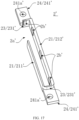
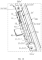
- FIG. 16 is an X-direction cross-sectional view at a position of a first connecting end 61 of a connection structure 6 in FIG. 15 .
- FIG. 16 illustrates a screw hole 100c for inserting a screw, a screw insertion connecting hole 241a and the screw hole 100c fix the bracket 2 to the middle frame 100.
- a certain spatial region is reserved from a region where the battery compartment 400 and the main board 200 are connected (that is, a region circled in FIG. 15 ).
- the connection structure 6 extends in the Y direction from the gap between the bracket 2 and the battery compartment 400 to a position at which the battery compartment 400 and the main board 200 are connected. Since a width of the main board 200 in the X direction is greater than a width of the battery compartment 400, the connection structure 6 needs to be bent at the connecting position, and a certain space is reserved at the connecting position to allow the connection structure 6 to be easily bent and extended to the side of the main board 200, and then folded and connected to the main board 200, so as to be connected to the main board connecting end 200a of the main board 200.
- FIG. 15 a certain spatial region is reserved from a region where the battery compartment 400 and the main board 200 are connected (that is, a region circled in FIG. 15 ).
- the connection structure 6 extends in the Y direction from the gap between the bracket 2 and the battery compartment 400 to a position
- a battery compartment on one side of the connection structure 6 may include a side wall of a certain thickness and strength as a retaining wall, so that the module assembly may be stably and reliably arranged between the side wall 100a of the middle frame 100 and a side wall of the battery compartment 400.
- connection structure 6 adopts a side-out scheme.
- the connection structure 6 may also adopt a straight-out scheme, that is, after the first connecting end 61 of the connection structure 6 is connected to the external connecting end 12 of the module 1, the connection structure 6 extends in the Z direction and is bent to a surface of the main board 200 to be connected to the main board connecting end 200a at a corresponding position.
- Such a mounting manner requires a sufficient Z-direction space in consideration of a bending radius of the connection structure 6 and a distance between a bending position and a BTB connection position. As shown in FIG.
- connection structure 6 is very limited when the connection structure 6 is straight out, and consequently, the first connecting end 61 and the module 1 may be disconnected, and the connection structure 6 cannot be fixed by using the second limiting part 21 of the bracket 2.
- the specific scheme of side out or straight out may be selected according to actual requirements.
- FIG. 17 is a schematic structural diagram of a bracket 2' according to Embodiment 2 of this application.
- FIG. 18 is a schematic diagram of a module assembly mounted in a middle frame 100 of a mobile phone according to Embodiment 2 of this application.
- FIG. 19 is a cross-sectional view taken along an X-direction in FIG. 18 , where a sectional position corresponds to a position of the bracket 2' on which an elastic part 2b' is not arranged.
- FIG. 20 is a cross-sectional view taken along an X-direction in FIG. 18 , where a sectional position corresponds to a position of the bracket 2' on which an elastic part 2b' is arranged.
- the bracket 2' includes two side plates arranged opposite to each other and two end plates 231' arranged opposite to each other.
- the end plate 231' is the first limiting part 23, and the side plate is the second limiting part 21.
- the two side plates are a first side plate 211' and a second side plate 212'.
- the two side plates and the two end plates 231' are enclosed to form a mounting position for mounting the module 1, where the module 1 herein has the same structure as the module 1 in Embodiment 1.
- an inner wall of at least one of the side plate or the end plate 231' is at least partially provided with an elastic part 2b' made of an elastic material in a protruding manner, so as to be in an interference fit with the module 1.
- an inner wall of at least one of the end plate 231', the first side plate 211', or the second side plate 212' includes the elastic part 2b'.
- the elastic part 2b' is only arranged on adjacent end plates 231' and the second side plates 212', to pressing the module 1 to be closer to the other end plates 231' and the first side plates 211', thereby facilitating in determining a position of the module 1.
- the elastic parts 2b may be uniformly distributed along a circumferential direction of the bracket 2', thereby facilitating in uniformly pressing the module 1.
- the elastic part 2b' arranged in the bracket 2' may press a side wall of the module 1, specifically, press the antenna module 14 and the chip 13 of the module 1.
- the elastic part 2b' may not cause damage to the module 1 due to elastic properties and forms an interference fit with the module 1 based on an elastic pressing action, thereby positioning the module 1.
- a height of any one of the two side plates or the two end plates 231' of the bracket 2' may be at least higher than one half of the height of the module 1, so as to limit and protect the module 1.
- the height of the bracket 2' may be set to about 1.0 mm.
- the two end plates 231', and the first side plates 211' and the second side plates 212' are also integrally formed.
- heights of the two end plates 231' and the two side plates may be processed to be the same. As shown in FIG.
- fixing plates 241' are further arranged on the end plate 231', the fixing plates 241' and the end plates 231' may be integrally or separately formed, both fixing plates 241' are provided with connecting holes 241a' and may be fixed to the middle frame 100 of the mobile phone by using screws passing through the corresponding connecting holes 241a'.
- the bracket 2, 2' in the embodiments of this application may also be directly formed in the middle frame 100, so that there is no need to arrange fixing parts, for example, a groove is provided in the middle frame 100, and a peripheral wall of the groove is used as the end plate and the side plate of the bracket 2'.
- a length of the first side plate 211' is less than that of the second side plate 212', and a second notch 2a'is formed between the first side plate 211' and an end plate 231'.
- the second notch 2a' also reserves a space, to facilitate connection between the external connecting end 12 of the module 1 and the connection structure 6. After the external connecting end 12 of the module 1 is connected to the connection structure 6, the two form a connecting position.
- Sizes of the first notch 2a in the first embodiment and the second notch 2a' in the second embodiment in the Y direction are to be reserved with the connecting position by about 0.5 mm, that is, connection between the external connecting end 12 and the connection structure 6 is avoided, to avoid scratching.
- the two end plates 231' and the two side plates of the bracket 2' form a circumferential nearly closed mounting position, and the bracket 2' may limit the module 1 in a circumferential direction except for a position of the second notch 2a'. In this way, limiting is reliable.
- the bottom of the bracket 2' may be empty, that is, a bottom plate is not arranged on the bracket 2', so that the module 1 is more convenient to mount, and the bracket 2' can be mounted from top to bottom or from bottom to top in the Z direction.
- a certain gap needs to be reserved between the bracket 2' and the middle frame 100 of the mobile phone or another component in the mobile phone in the X direction and Y direction, to avoid scratching, for example, the gap may be set to about 0.1 mm.
- the two end plates 231' and the two side plates may be integrally molded, and the elastic part 2b' is made of soft plastic, which may be, for example, thermoplastic polyurethane (TPU, Thermoplastic Urethane).
- TPU thermoplastic polyurethane
- Other parts of the bracket 2' are made of hard material, for example, which may specifically be molded by performing a double-shot injection molding process, or may be molded by LIM (which is a liquid silicone process).
- the processed bracket 2' includes R angles at transition and edge positions of the first side plate 211', the second side plate 212', and the end plate 23 1', and a processed mold also has own mold R angles at non-R angle positions corresponding to the bracket 2', so that a surface of the bracket 2' formed by processing is smoother, and the connection structure 6 may be effectively prevented from being scratched.
- the strength and reliability of the bracket 2' may be ensured by integrally injection molding the hard plastic and the soft plastic, and a bracket 2' in a desired shape may be easily molded.
- one side of the bracket 2' mentioned in Embodiment 1 is provided with an opening on one side, to avoid an external radiation region of the antenna module 14 of the module 1.
- the bracket 2' in this embodiment is made of hard plastic and soft plastic. Compared with metal, it has limited influence on the function of the antenna module 14 of the module 1, that is, material with little or no influence on the communication performance may be selected as the material of the bracket 2'.
- the elastic part 2b' made of soft plastic of the bracket 2' may be in an interference limit with the module 1, and limiting requirements are considered.
- the bracket 2' is made of hard plastic and soft plastic, which has a certain heat dissipation effect.
- bracket 2 which are specifically made of soft plastic, but the soft plastic and hard plastic are not limited to only two materials, and the bracket 2' may be made of two or more materials, where the soft plastic realizes elastic interference fit, and the hard plastic meets strength requirements of the bracket 2'.
- FIG. 21a to FIG. 21c are three schematic structural diagrams of arranging elastic parts 2b' on a second side plates 212' of a bracket 2' according to Embodiment 2.
- a first structure of the elastic part 2b' shown in FIG. 21a is in a trapezoidal elastic part 2b'
- a second elastic part 2b' shown in FIG. 21b is in a triangular shape
- a third elastic part 2b' shown in FIG. 21c is in an elliptical shape.
- FIG. 22 is a cross-sectional view taken along an X-direction at a position of a circuit board element 7 in FIG. 18 .
- a circuit board element 7 may also be arranged on the bottom of the module assembly.
- the bottom of the bracket 2' is empty and no bottom plate 22 is arranged.
- the circuit board element 7 may be fixed to the bottom of the module 1, which may be, for example, bonded to the module 1 by using the back adhesive 51.
- FIG. 23 is a schematic diagram of another manner of arranging a circuit board element 7 on the bottom of a bracket 2' according to Embodiment 2.
- a bottom plate may also be arranged on the bracket 2' in Embodiment 2 or a fixed structure may be arranged on the bottom.
- the fixing structure is, for example, an extension plate 26 extending from an edge of the first side plate 211' to the second side 212', and the extension plate 26 may cover part or all of the bottom of the bracket 2', which is equivalent to arranging a bottom plate.
- the circuit board element 7 may be fixed to the fixing structure on the bottom of the bracket 2' by using a back adhesive or other fasteners, and a limiting structure as shown in Embodiment 1 may be arranged on the bottom of the fixing structure, to limit the circuit board element 7. Details are not described herein again. As can be seen, if a fixing structure is arranged on the bracket 2', it is obvious that the module 1 needs to be mounted from a side opposite to the bottom plate.
- FIG. 24 is a cross-sectional view taken along an X-direction at a position of a heat conductive pad 4 in FIG. 18 .
- a heat conductive pad 4 may be provided on the bottom of the bracket 2', and the heat conductive pad 4 may be directly arranged between the bottom of the module 1 and the bottom wall 100b of the middle frame 100 as shown in FIG. 24 , where the heat conductive pad 4 is in direct contact with the bottom of the module 1, which has better heat conduction and heat dissipation effects.
- the bottom of the module 1 is protruded from the bracket 2', so that a gap between the module 1 and the bottom wall 100b of the middle frame 100 is smaller.
- the heat conductive pad 4 is arranged without interference from the bottom of the first side plate 211' and the second side plate 212' of the bracket 2', so that the heat conductive pad 4 may be fully contacted with the module 1.
- the heat conductive pad 4 may also be arranged between the support 2' and the bottom wall 100b of the middle frame 100, for example, if the bracket 2' is protruded about 0.5 mm or more, or the circuit board element 7 may be fixed with a fixing structure as shown in FIG. 23 , and a bottom plate or another structure may be arranged on bottom of the bracket 2'.
- the heat conductive pad 4 may also be arranged between the bottom plate or another structure and the middle frame 100.
- connection structure 6 may be mounted in a side-out or straight-out manner, and the main body portion 63 of the connection structure 6 may be fixed to the second side plate 212' that is used as the second limiting part 21, which may be understood with reference to Embodiment 1. Details are not described herein again.
- the description is made mainly by using an example in which the module 1 is a millimeter wave module.
- the bracket provided in this embodiment of this application may also configured to mount a module 1 of another type.
- the module 1 is not limited to the antenna module 14, the chip 13, and the external connecting end 12 which can transmit signals, and any module structure needs to be assembled into the electronic device may be mounted by using the bracket provided in this embodiment of this application.
- the bracket mainly aims to limit and protect the module. When the structure of the module changes accordingly, the size and shape of a mounting position formed by the bracket may be adjusted accordingly.
- the bracket 2 and the middle frame 100 of the mobile phone are separately arranged.
- the bracket 2 may also be integrally formed in the middle frame 100 of the mobile phone, and particularly, for an interference fit scheme in Embodiment 2, it is easy to be integrally formed in the middle frame 100.
- the middle frame 100 may be formed into a groove, the groove is used as the mounting position of the module 1, the middle frame 100 made of metal is usually used as a hard part, and then an elastic part made of elastic material is arranged on a groove wall, and the elastic part may be injection molded with the middle frame 100, or the elastic part may be embedded in the groove wall provided by the middle frame 100.
- the above-mentioned embodiment is described by using an example in which the module assembly is mounted to the middle frame 100 of the mobile phone.
- the bracket provided in the embodiments of this application may also be used for mounting.
- the electronic device may also be, for example, a mobile terminal such as a mobile phone, a wearable device, a vehicle-mounted device, an augmented reality (augmented reality, AR)/virtual reality (virtual reality, VR) device, an ultra-mobile personal computer (ultra-mobile personal computer, UMPC), a netbook, a personal digital assistant (personal digital assistant, PDA), or may be a professional shooting device such as a digital camera, an SLR camera/micro-single camera, a motion camera, a pan/tilt camera, an unmanned aerial vehicle as long as it is an electronic device with a module. This is not specifically limited in this scheme.
- a mobile terminal such as a mobile phone, a wearable device, a vehicle-mounted device, an augmented reality (augmented reality, AR)/virtual reality (virtual reality, VR) device, an ultra-mobile personal computer (ultra-mobile personal computer, UMPC), a netbook, a personal digital assistant (personal digital assistant, PDA), or may be
Landscapes
- Engineering & Computer Science (AREA)
- Computer Hardware Design (AREA)
- Theoretical Computer Science (AREA)
- General Engineering & Computer Science (AREA)
- Physics & Mathematics (AREA)
- Signal Processing (AREA)
- Human Computer Interaction (AREA)
- General Physics & Mathematics (AREA)
- Thermal Sciences (AREA)
- Microelectronics & Electronic Packaging (AREA)
- Computer Networks & Wireless Communication (AREA)
- Telephone Set Structure (AREA)
Abstract
Description
- This application claims priority to
Chinese Patent Application No. 202111562886.5, filed with the China National Intellectual Property Administration on December 20, 2021 Chinese Patent Application No. 202210197522.X, filed with the China National Intellectual Property Administration on March 1, 2022 - This application relates to the field of electronic technologies, and in particular, to a bracket, a module assembly, and an electronic device.
- With the continuous development of communication technology, users' requirements for communication performance of electronic devices are increasingly higher. To meet use requirements of the users for electronic device communication in different occasions and scenarios, some modules with special communication performance, such as a millimeter wave module, may be incorporated into electronic products such as mobile phones. The main function of such a module is to realize signal transmission in a millimeter wave band.
- Current millimeter wave modules are usually packaged devices, including a circuit board, a chip, an antenna module, and a BTB (Board to Board) connector, which are configured to connect to a circuit board in the mobile phone. After the millimeter wave module is mounted in the mobile phone, position stability and connection stability need to be maintained.
- Embodiments of this application provide a bracket, a module assembly, and an electronic device, which may mount a module more stably, to improve position stability of the module in the electronic device.
- According to an aspect, an embodiment of this application provides a bracket for a module, two first limiting parts arranged opposite to each other are arranged at two ends of the bracket, a second limiting part is arranged on at least one side of the bracket, and the two first limiting parts and the second limiting part are enclosed to form a mounting position for mounting the module. Two first limiting parts at two ends and a second limiting part at least at one side are enclosed to form a mounting position, and both the first limiting parts and the second limiting part may limit the module, so as to limit in all directions and ensure position stability of the module in the bracket. The bracket is further fixed to the electronic device through fixing parts, so that the position stability of the module in the electronic device may be ensured.
- According to an aspect, an embodiment of this application further provides a first implementation according to the aspect.
- The bracket includes a bottom plate and vertical plates at two ends of the bottom plate, and the vertical plates form the first limiting parts; and a first flange is arranged on only one side of the bottom plate, and the first flange forms the second limiting part. A bottom plate is further arranged while two first limiting parts and one second limiting part are arranged, and the bottom plate may provide a better supporting role for the module, to further ensure mounting on the module in a limited manner.
- According to the first implementation of the aspect, an embodiment of this application further provides a second implementation according to the aspect.
- A second flange opposite to an extension direction of the first flange is arranged on the other side of the bottom plate, and the second flange is configured to bond a circuit board element and/or an electronic device. The second flange may bond the circuit board element and the electronic device, thereby facilitating fixing of the circuit board element and improving reliability of connection between the bracket and the electronic device.
- According to the first implementation of the aspect, an embodiment of this application further provides a third implementation according to the aspect.
- The bracket is made of copper alloy or carbon fiber. Copper alloy and carbon fiber have high strength, meet strength requirements, and have good heat dissipation performance, which is also beneficial to heat dissipation of the module in a case that heat dissipation is required, thereby improving user experience.
- According to an aspect, an embodiment of this application further provides a fourth implementation according to the aspect.
- The bracket includes two side plates arranged opposite to each other and two end plates arranged opposite to each other, the end plate is the first limiting part, and the side plate is the second limiting part; and the two side plates and the two end plates are enclosed to form the mounting position, and an inner wall of at least one of the side plate or the end plate is at least partially provided with an elastic part made of an elastic material in a protruding manner, so as to be in an interference fit with the module. The bracket is enclosed by two first limiting parts and two second limiting parts to form a mounting position, to limit the module more comprehensively in a circumferential direction, and limit is realized by interference pressing of the elastic part, so that limit is reliable and may not damage the module. The bottom of the bracket may also be empty by performing interference pressing, so that it is more convenient to mount the module, and the module assembly is not easy to float after mounting.
- According to the fourth implementation of the aspect, an embodiment of this application further provides a fifth implementation according to the aspect.
- The end plate and the side plate are integrally formed through injection molding, the elastic part is made of soft plastic, and other parts of the end plate and the side plate are made of hard plastic. Integrated injection molding is beneficial to ensuring integration of the bracket, and the elastic part is not prone to be separated from other parts. The soft plastic is beneficial to realizing interference pressing, and the hard plastic part is beneficial to ensuring the strength of the bracket. In addition, when the module has a signal transmission function, the plastic material has no or little influence on the function of the module.
- According to an aspect and the first implementation to the fifth implementation of the aspect, an embodiment of this application further provides a sixth implementation according to the aspect.
- The module includes an external connecting end, and the bracket is provided with a notch to expose the external connecting end. The notch is arranged to expose the external connecting end, so as to facilitate connection between the external connecting end and the external components, and avoid scratching the external connecting end or connected external components.
- According to an aspect and the first implementation to the fifth implementation of the aspect, an embodiment of this application further provides a seventh implementation according to the aspect.
- The bracket is separately arranged on the electronic device, and the bracket includes fixing parts, where the fixing parts are configured to fix the bracket to the electronic device; or the bracket is integrally formed on a housing of the electronic device. The bracket is integrally arranged on the housing of the electronic device, and there is no need to perform a fixing operation. Alternatively, the bracket is separately arranged in the electronic device, which is convenient to process.
- According to the seventh implementation of the aspect, an embodiment of this application further provides an eighth implementation according to the aspect.
- The bracket is separately arranged on the electronic device, the fixing parts are fixed or integrally arranged on the first limiting parts, and the fixing parts are provided with connecting holes configured for fixing to the electronic device. The fixing part is arranged on the first limiting part, that is, at two ends of the bracket, and connecting holes are provided, thereby facilitating implementation of a fastening operation.
- According to a second aspect, an embodiment of this application further provides a module assembly, including a module and a bracket for mounting the module. The bracket is a bracket according to an aspect and the first implementation to the eighth implementation of the aspect, and the module is mounted at the mounting position of the bracket. The module assembly has the same technical effect as the bracket.
- According to a second aspect, an embodiment of this application further provides a first implementation according to the second aspect.
- The module includes an external connecting end, and the module assembly further includes a connection structure, where the connection structure includes a main body portion and a first connecting end and a second connecting end that are arranged on the main body portion, the first connecting end is configured to be connected to the external connecting end of the
module 1, and the second connecting end is configured to connect an electronic element of the electronic device; and the main body portion is capable of being fixed to the second limiting part. The main body portion of the connection structure is fixed to the second limiting part, so that connection between the first connecting end and the second connecting end does not interfere with each other, and the connection reliability is higher. - According to the first implementation of the second aspect, an embodiment of this application further provides a second implementation according to the second aspect.
- The main body portion is bonded to the second limiting part. Such a bonding manner is simple and may not damage the connection structure.
- According to the second aspect and the first implementation and the second implementation of the second aspect, an embodiment of this application further provides a third implementation according to the second aspect.
- At least one of a heat conductive pad or a circuit board element is fixed on the bottom of the module assembly. The heat conductive pad is arranged on the bottom of the module assembly, which can effectively improve the heat dissipation effect of the module assembly and improve the user experience. The heat conductive pad is arranged on the bottom of the module assembly, which may not be damaged during the mounting, thereby maintain the heat conduction performance. When the circuit board element is arranged on the bottom of the module assembly, the module assembly is simultaneously used as a mounting part of the circuit board element, thereby making full use of a space.
- According to the third implementation of the second aspect, an embodiment of this application further provides a fourth implementation according to the second aspect.
- A limiting structure is arranged on the bottom of the bracket, and the limiting structure prevents the circuit board element from being separated from the bottom. The circuit board element is limited by the limiting structure, which is beneficial to ensuring the position stability of the circuit board element in the electronic device.
- According to the fourth implementation of the second aspect, an embodiment of this application further provides a fifth implementation according to the second aspect.
- The limiting structure is a protrusion or concave part arranged on the bottom of the bracket, and the circuit board element includes a corresponding concave part or protrusion; or the limiting structure is a concave part arranged on the bottom of the bracket, and the circuit board element is capable of being embedded into the concave part. The limit is simple based on convex-concave coordination, and it is easy to realize limit and process the structure.
- According to the second aspect and the first implementation and the second implementation of the second aspect, an embodiment of this application further provides a sixth implementation according to the second aspect.
- A bottom plate is arranged on the bottom of the bracket, and the bottom of the module is bonded to the bottom plate. The module is bonded to the bottom plate, which may further improve the position stability of the module in the bracket.
- According to the second aspect and the first implementation and the second implementation of the second aspect, an embodiment of this application further provides a seventh implementation according to the second aspect.
- The module is bonded to at least one of the first limiting part or the second limiting part. The module is connected to the first limiting parts and the second limiting part, which may further improve the position stability of the module in the bracket.
- According to the seventh implementation of the second aspect, an embodiment of this application further provides an eighth implementation according to the second aspect.
- The module includes a chip, where the chip is bonded to the second limiting part. The chip may have a heat generating component bonded to the second limiting part, to accelerate heat dissipation.
- According to the second aspect and the first implementation and the second implementation of the second aspect, an embodiment of this application further provides a ninth implementation according to the second aspect.
- The module includes an antenna module capable of performing communication, the second limiting part is arranged on only one side of the bracket, the other side of the bracket is provided with an opening, and the antenna module faces the opening. The antenna module faces the opening, that is, the opening is in an external radiation region of the antenna module, so that the communication function of the antenna module may not be affected.
- According to the second aspect and the first implementation to the ninth implementation of the second aspect, an embodiment of this application further provides a tenth implementation according to the second aspect.
- The module is a millimeter wave module. The millimeter wave module may transmit signals in a millimeter wave band. By using the bracket in this embodiment, the millimeter wave module can be stably arranged in the electronic device to stably transmit signals.
- According to a third aspect, an embodiment of this application further provides an electronic device including the module assembly according to the second aspect and any one of the first to tenth implementations of the second aspect. The electronic device has the same technical effect as the module assembly.
- According to a third aspect, an embodiment of this application further provides a first implementation according to the third aspect.
- The electronic device is a mobile phone, and the module assembly is arranged in a middle frame of the mobile phone. The module assembly is arranged in the middle frame, which can be fixed through the middle frame and is convenient to mount.
- According to the first implementation of the third aspect, an embodiment of this application further provides a second implementation according to the third aspect.
- A heat conductive pad is arranged between the bottom of the module assembly and a bottom wall of the middle frame. The heat conductive pad may guide heat of the module to the bottom wall of the middle frame as soon as possible, so as to achieve the purpose of dissipating heat to the outside.
-
-
FIG. 1 is a schematic diagram of a module according toEmbodiment 1 of this application. -
FIG. 2 is a schematic structural diagram of a bracket according toEmbodiment 1 of this application. -
FIG. 3 is a schematic structural diagram of the bracket inFIG. 2 from another perspective. -
FIG. 4 is a schematic diagram of a module assembly formed by mounting the module inFIG. 1 on the bracket inFIG. 2 . -
FIG. 5 is a schematic diagram of the module assembly inFIG. 4 arranged in a middle frame of a mobile phone. -
FIG. 6 is a top view ofFIG. 5 . -
FIG. 7 is a cross-sectional view taken along a line A-A ofFIG. 6 . -
FIG. 8 is a schematic diagram of arranging a circuit board element on the bottom of the bracket inFIG. 7 . -
FIG. 9 is a schematic diagram of a circuit board element with a first limiting structure arranged the bottom of the bracket inFIG. 3 . -
FIG. 10 is a schematic diagram of a circuit board element with a second limiting structure arranged the bottom of the bracket inFIG. 3 . -
FIG. 11 is a schematic diagram of a circuit board element with a third limiting structure arranged the bottom of the bracket inFIG. 3 . -
FIG. 12 is a cross-sectional view taken along a line B-B ofFIG. 6 . -
FIG. 13 is an enlarged view at a position of an external connecting end inFIG. 6 . -
FIG. 14 is a schematic diagram of a connection structure inFIG. 6 . -
FIG. 15 is a schematic diagram of a module assembly shown inFIG. 4 arranged in a middle frame of a mobile phone and located on one side of a battery compartment. -
FIG. 16 is an X-direction cross-sectional view at a position of a first connecting end of a connection structure inFIG. 15 . -
FIG. 17 is a schematic structural diagram of a bracket according toEmbodiment 2 of this application. -
FIG. 18 is a schematic diagram of a module assembly mounted in a middle frame of a mobile phone according toEmbodiment 2 of this application. -
FIG. 19 is a cross-sectional view taken along an X-direction inFIG. 18 . -
FIG. 20 is a cross-sectional view taken along an X-direction inFIG. 18 . -
FIG. 21a is a first schematic structural diagram of arranging an elastic part on a second side plate of a bracket according toEmbodiment 2. -
FIG. 21b is a second schematic structural diagram of arranging an elastic part on a second side plate of a bracket according to anembodiment 2. -
FIG. 21c is a third schematic structural diagram of arranging an elastic part on a second side plate of a bracket according toEmbodiment 2. -
FIG. 22 is a cross-sectional view taken along an X-direction at a position of a circuit board element inFIG. 18 . -
FIG. 23 is a schematic diagram of another manner of arranging a circuit board element on the bottom of a bracket according toEmbodiment 2. -
FIG. 24 is a cross-sectional view taken along an X-direction at a position of a heat conductive pad inFIG. 18 . - Referring to
FIG. 1, FIG. 1 is a schematic diagram of amodule 1 according toEmbodiment 1 of this application. - The
module 1 in this embodiment of this application is specifically a millimeter wave module and is mainly configured to achieve signal transmission in a millimeter wave band. As shown inFIG. 1 , the millimeter wave module includes acircuit board 11, a plurality ofantenna modules 14 arranged on one side of thecircuit board 11 configured to realize communication, achip 13 arranged on the other side of thecircuit board 11, and an external connectingend 12. The external connectingend 12 is, for example, a BTB connector, and the external connectingend 12 may connect the millimeter wave module to a circuit board element of a mobile phone, for example, to amain board 200 of the mobile phone. - The
module 1 may be mounted in abracket 2, and the two are assembled into a module assembly. The module assembly is mounted into the electronic device. The module assembly in this embodiment of this application is specifically mounted in amiddle frame 100 of the mobile phone, which may be understood with reference toFIG. 2 to FIG. 6 .FIG. 2 is a schematic structural diagram of arranging a heatconductive pad 4 and a back adhesive 51 on thebracket 2 according toEmbodiment 1.FIG. 3 is a schematic structural diagram of abracket 2 inFIG. 2 from another perspective.FIG. 4 is a schematic diagram of a module assembly formed by mounting themodule 1 inFIG. 1 on thebracket 2 inFIG. 2 .FIG. 5 is a schematic diagram of the module assembly inFIG. 4 arranged in amiddle frame 100 of a mobile phone.FIG. 6 is a top view ofFIG. 5 . - As shown in
FIG. 2 andFIG. 3 , two first limitingparts 23 arranged opposite to each other are arranged at two ends of thebracket 2 of the module assembly, a second limitingpart 21 is arranged on one side of thebracket 2, and the two first limitingparts 23 and one second limitingpart 21 are enclosed to form a mounting position for mounting themodule 1. Specifically, thebracket 2 includes abottom plate 22 and vertical plates 231 located at two ends of thebottom plate 22. The vertical plates 231 form the first limitingparts 23. A first flange 211 is arranged on only one side of thebottom plate 22, and the first flange 211 forms the second limitingpart 21. During mounting, from the perspective ofFIG. 4 , themodule 1 is arranged on thebottom plate 22, and one side of themodule 1 is limited by the first flange 211 that is used as the second limitingpart 21. As shown inFIG. 4 , one side on which achip 13 is arranged in themodule 1 is limited by the first flange 211, and two ends of themodule 1 are limited by the vertical plates 231 that are used as the first limitingparts 23. - The
bracket 2 further includes fixing parts 24, where the fixing parts 24 are configured to fix thebracket 2 to themiddle frame 100 of the mobile phone. InFIG. 3 , edges of the vertical plates 231 far away from thebottom plate 22 extend in directions far away from the mounting position to form fixingflanges 241, and the fixingflanges 241 are used as the fixing parts 24. Connectingholes 241a are provided on the fixingflanges 241, and thebracket 2 may be fixed to themiddle frame 100 of the mobile phone by inserting screws into the corresponding connectingholes 241a. Certainly, the fixing part 24 may also be arranged on another position of thebracket 2, for example, may be separately fixed to the bottom or a side edge of thebracket 2, which is mainly designed according to a mounting position of the module assembly in the mobile phone, to facilitate fastening. In this embodiment, the fixingflanges 241, the vertical plates 231, thebottom plate 22, and the first flange 211 are all integrally formed, which have better strength and are easy to process. - As shown in
FIG. 5 , during the mounting, thebracket 2 may be first fixed in themiddle frame 100, and then themodule 1 is mounted, or thebracket 2 and themodule 1 may be assembled into the module assembly, and then the assembly may be integrally mounted in themiddle frame 100. - Two first limiting
parts 23 and one second limitingpart 21 of thebracket 2 need to have a certain limiting effect on themodule 1, to maintain the position stability of themodule 1 on thebracket 2. A distance between the two first limitingparts 23, that is, a length of thebottom plate 22 is slightly longer than a length of themodule 1. In consideration of factors such as a tolerance of the module and a processing tolerance of thebracket 2, for example, a gap may be 0.1 mm, themodule 1 is mounted to thebracket 2 in a top-edge alignment manner, that is, the two ends of themodule 1 and the first limitingparts 23 are zero-matched, and then themodule 1 is fixed to the second limitingpart 21 by using a back adhesive, so that it is convenient for mounting without damaging themodule 1, and limiting is achieved. Thebracket 2 is made of copper alloy (such as C1940 alloy), a carbon fiber, or other materials with certain strength, and such material may have better heat dissipation performance, to facilitate themodule 1 in heat dissipation. The material of thebracket 2 is not limited as long as it meets strength requirements of mounting and protecting themodule 1, and it is better to consider certain heat dissipation performance. - Still referring to
FIG. 3 , a length of the first flange 211 of thebracket 2 is less than a length of a corresponding side of thebottom plate 22, that is, the first flange 211 is not arranged on one side of thebottom plate 22 in an entire length direction. In this case, since the length of the first flange 211 is less than the length of one side of thebottom plate 22, the first flange 211 is connected to a vertical plate 231 at an end of thebottom plate 22, and there is a gap therebetween. The gap may be defined as afirst notch 2a. With reference toFIG. 3 and FIG. 4 , it is to be understood that, after themodule 1 is mounted to thebracket 2, thefirst notch 2a corresponds to an external connectingend 12 of themodule 1, so that the external connectingend 12 establishes a connection to an external element at a position of thefirst notch 2a. In other words, a position is reserved to avoid the external connectingend 12, to prevent thebracket 2 from interfering with connection of the external connectingend 12 and scratching the external connectingend 12. - As shown in
FIG. 3 , thefirst notch 2a is reserved between one end of the first flange 211 and a vertical plate 231 at one end of thebottom plate 22, and the other end of the first flange 211 and a vertical plate 231 at the other end of thebottom plate 22 may have a relatively small gap therebetween or may be connected to each other. In other words, in addition to reserving the necessaryfirst notch 2a, the length of the first flange 211 may be as long as possible, to improve a capability of limiting themodule 1. For example, the length of the first flange 211 may be exceed half of the length of themodule 1, where the length of themodule 1 is a size of themodule 1 in an arrangement direction of a plurality ofantenna modules 14 inFIG. 1 . In this embodiment, the length of themodule 1 is basically the same as the length of thebottom plate 22, to achieve zero matching with the vertical plates 231 at two ends as much as possible. For example, the length of themodule 1 is slightly less than the length of thebottom plate 22. In this way, smooth assembly and a limiting effect of the vertical plates 231 at two ends after assembly may be ensured. Therefore, the length of the first flange 211 exceeds half of the length of thebottom plate 22 in this case. It may be understood that, thefirst notch 2a is not limited to be provided between the first flange 211 and one vertical plate 231, which may be designed according to a position of the external connectingend 12 on themodule 1. For example, in a case that the external connectingend 12 is located in the middle of themodule 1, the first flange 211 may reserve a corresponding notch in the middle. In another example, themodule 1 may also arrange more external connecting ends 12, and the first flange 211 may also correspondingly provide a corresponding quantity of notches, or one notch may avoid all the external connecting ends 12. - In addition, a height of the first flange 211 may be set to be higher than half of a height of the
module 1, to ensure that themodule 1 is limited. A height direction herein is a depth direction of the mounting position formed by enclosing the first flange 211 and the vertical plates 231 at two ends. From the perspective ofFIG. 6 , an X direction shown inFIG. 6 is a width direction of the mobile phone, a Y direction is a length direction of the mobile phone, and the height is a size of the first flange 211 in a Z direction perpendicular to a paper direction. It may be seen that a height of at least one of the first limitingpart 23 or the second limitingpart 21 is higher than half of the height of themodule 1. Certainly, it is preferable that the height of the first limitingpart 23 and the second limitingpart 21 is higher than half of the height of themodule 1. The first flange 211 inFIG. 3 is set to a higher height. A height of the vertical plates 231 whose two ends are used as the first limitingparts 23 is less than that of the first flange 211. This is mainly because the fixingflanges 241 arranged by two vertical plates 231 and themiddle frame 100 are limited by a fixed position when fixed. It may be seen that, according to structural design of themiddle frame 100, the vertical plates 231 may be higher in a case that there is no interference and restriction. For example, themiddle frame 100 may be higher than themodule 1. Actually, the height of at least one of the first limitingpart 23 and the second limitingpart 21 is preferably higher than that of themodule 1, for example, the height may exceed more than 0.15 mm. In this way, in consideration of the tolerance of themodule 1 and the processing tolerance of thebracket 2, themodule 1 may not protrude from thebracket 2 in a height direction, so that thebracket 2 may be better limited and protect themodule 1 from being scratched during assembly. For the same reason, the height of the vertical plate 231 may also higher than half of the height of themodule 1. - In addition, a certain floating height may be generated after the
module 1 and thebracket 2 are assembled. After the module assembly is assembled into themiddle frame 100 of the mobile phone, there may be a gap between a highest position of the module assembly and abattery cover 300, to avoid film printing on thebattery cover 300 of the mobile phone. For example, the gap may be about 0.25 mm. A plug structure may further be arranged, and the plug structure is plugged between the module assembly and the battery cover 300 (shown inFIG. 7 ), to prevent the module assembly from being separated in the Z direction. A gap may also be reserved between the first flange 211 of thebracket 2 and themiddle frame 100 or another component in the mobile phone in the X direction and Y direction, to meet requirements of assembly and positioning. For example, the gap may be about 0.1 mm. - Still referring to
FIG. 3 , in this embodiment of this application, asecond flange 25 opposite to an extension direction of the first flange 211 is arranged on the other side of thebottom plate 22, and thesecond flange 25 and thebottom plate 22 may be integrated. With reference toFIG. 7 , it may be understood that,FIG. 7 is a cross-sectional view taken along a line A-A ofFIG. 6 , which is sectioned at a position of thesecond flange 25. As shown inFIG. 7 , the arrangedsecond flange 25 may be configured to bond themiddle frame 100. InFIG. 7 , thesecond flange 25 is bonded to themiddle frame 100 by using aback adhesive 54, and thesecond flange 25 may also abut against themiddle frame 100 to play a role of limiting. - The
middle frame 100 includes abottom wall 100b and aside wall 100a surrounding thebottom wall 100b. With reference toFIG. 5 andFIG. 7 , it may be understood that themodule 1 in this embodiment is a millimeter wave module. In this embodiment, the first flange 211 is arranged on only one side of thebottom plate 22 of thebracket 2 and is used as the second limitingpart 21, and the other side is empty and form an opening, so that two first limitingparts 23 and thefirst flange 212 used as the second limitingpart 21 are enclosed to form a mounting position having an opening on one side, and thebracket 2 is assembled into themiddle frame 100 and is located close to theside wall 100a of themiddle frame 100. The first flange 211 is relatively far away from theside wall 100a of themiddle frame 100, and one side of the opening of thebracket 2 where the first flange 211 is not arranged is close to theside wall 100a of themiddle frame 100. During the mounting, theantenna module 14 of themodule 1 may face one side of the opening of thebracket 2, the opening is provided in an external radiation region, and theantenna module 14 may be arranged close to theside wall 100a of themiddle frame 100. In this case, theantenna module 14 is not limited and blocked by one side of the opening of thebracket 2, that is, thebracket 2 may not arrange a limiting part in the external radiation region of themodule 1, which is more conducive to signal transmission between themillimeter wave module 1 and the outside. It may be understood that, in a case that thebracket 2 is not made of metal and the corresponding second limitingpart 21 is made of material with good thermal conductivity and insulation performance, the second limiting parts 211 may also be arranged on two sides of thebracket 2. From the perspective ofFIG. 6 , a region in which theantenna module 14 in themodule 1 faces theside wall 100a of themiddle frame 100 and transmit signals to the right is the external radiation region. - Based on this, a
second flange 25 opposite to an extension direction of the first flange 211 is arranged on one side of thebracket 2 where the first flange 211 is not arranged, and thesecond flange 25 is not located in the external radiation region of themodule 1. In addition, thesecond flange 25 may abut against the side wall of themiddle frame 100 to play a role of limiting and positioning, or may be fixed to themiddle frame 100 by using theback adhesive 54, to further ensure the position stability of the module assembly in themiddle frame 100. - As shown in
FIG. 7 , a back adhesive 51 may also be arranged on the bottom of thebottom plate 22 of thebracket 2, and the back adhesive 51 may be configured to bond an electronic element, that is, thebottom plate 22 of thebracket 2 may further used as a component for mounting the electronic element, thereby making full use of thebracket 2 of the module assembly and improving a space utilization rate. - Still referring to
FIG. 8, FIG. 8 is a schematic diagram of arranging acircuit board element 7 on the bottom of abracket 2 inFIG. 7 . A circuit board, that is, amain board 200 of the mobile phone is arranged in themiddle frame 100 of the mobile phone, in a case that themain board 200 has a limited area for use, thecircuit board element 7 may be added, for example, some small circuit boards smaller than themain board 200, and the addedcircuit board element 7 may be fixed to the bottom of thebottom plate 22 of thebracket 2, for example, thecircuit board element 7 may be bonded by using the back adhesive 51 or may be fastened to the bottom of thebracket 2 by using other fasteners. InFIG. 8 , during arrangement of thesecond flange 25, thesecond flange 25 may further limit a position of thecircuit board element 7, and may bond a side wall of thecircuit board element 7, to improve position stability of thecircuit board element 7. - With reference to
FIG. 9 to FIG. 11 , it may be understood that,FIG. 9 is a schematic diagram of acircuit board element 7 with a first limiting structure arranged the bottom of thebracket 2 inFIG. 3 ;FIG. 10 is a schematic diagram of acircuit board element 7 with a second limiting structure arranged the bottom of thebracket 2 inFIG. 3 ; andFIG. 11 is a schematic diagram of acircuit board element 7 with a third limiting structure arranged the bottom of thebracket 2 inFIG. 3 . - In a case that the
circuit board element 7 is arranged on the bottom of thebottom plate 22 of thebracket 2, a limiting structure may be arranged to limitcircuit board element 7, to ensure the position stability of thecircuit board element 7, where the limiting structure may be a protrusion. As shown inFIG. 9 , protrusions may be arranged on the bottom of thebottom plate 22 of thebracket 2, and thecircuit board element 7 may be provided with a corresponding hole structure. The protrusions may be a circular protrusion 2c1 and an elliptical protrusion 2c2 shown inFIG. 9 , and the hole structure may be a circular hole or an elliptical hole provided in thecircuit board element 7. The protrusions are inserted into the corresponding hole structure to limit thecircuit board element 7 specifically in the X direction and the Y direction. As shown inFIG. 10 , protrusions may also be arranged on the bottom ofbottom plate 22 of thebracket 2, and the protrusions may be an elliptical protrusion 2c3 and an elliptical protrusion 2c4 shown inFIG. 10 . A notch may be provided on an edge of thecircuit board element 7, and a part of the protrusions may be clamped into the notch or may play a role of limiting. As shown inFIG. 11 , a protrusion may also be arranged on the bottom ofbottom plate 22 of thebracket 2, and the protrusion is a frame-type protrusion 2c5. The entirecircuit board element 7 is embedded into the frame-type protrusion 2c5 to play a role of limiting. With reference toFIG. 8 , it may be understood that, thecircuit board element 7 may be bonded to the bottom of thebottom plate 22 of thebracket 2 by using the back adhesive 51 while being limited by the limiting structure, to ensure more stable and reliable connection of thecircuit board element 7. - Still referring to
FIG. 2 , it may be understood with reference toFIG. 12 that,FIG. 12 is a cross-sectional view taken along a line B-B ofFIG. 6 , which is sectioned at a position of a heatconductive pad 4. - In this embodiment, the heat
conductive pad 4 may be arranged between the bottom of thebottom plate 22 of thebracket 2 and thebottom wall 100b of themiddle frame 100, and the heatconductive pad 4 is arranged on the bottom. During the assembly, thebracket 2 may be assembled into themiddle frame 100 of the mobile phone in the Z direction, so that the heatconductive pad 4 may not be scratched and may maintain good heat conduction performance. Heat dissipated by themodule 1 may be transferred to the heatconductive pad 4 through thebottom plate 22 of thebracket 2, then transferred to themiddle frame 100 through the heatconductive pad 4, and is finally dissipated to the outside, thereby thus playing a good role of heat dissipation. The material of the heatconductive pad 4 is not limited, which may be, for example, a heat conductive adhesive, a heat pipe, a graphite sheet, and the like. A thermally conductive gel may also be used as the heatconductive pad 4 in a case that a space in the Z direction is limited, that is, a gap between thebottom plate 22 and thebottom wall 100b of themiddle frame 100 is relatively small. - As can be seen, in
FIG. 7 , the back adhesive 54 between thesecond flange 25 and an inner wall of themiddle frame 100 may also form the heat conductive pad. The back adhesive 54 may be a thermally conductive gel arranged between thesecond flange 25 and the inner wall of themiddle frame 100 in a case that an X-direction gap between thesecond flange 25 and the inner wall of themiddle frame 100 is relatively small, which may also play a role of heat conduction and facilitating in heat dissipation. - Referring to
FIG. 6 andFIG. 13 again,FIG. 13 is an enlarged view at a position of an external connectingend 12 inFIG. 6 ; andFIG. 14 is a schematic diagram of aconnection structure 6 inFIG. 6 . - In this embodiment, the module assembly further includes a
connection structure 6. The connection structure includes amain body portion 63, and a first connectingend 61 and a second connectingend 62 arranged on themain body portion 63. The first connectingend 61 is configured to connect the external connectingend 12 of themodule 1, and the second connectingend 62 is configured to connect the electronic element of the electronic device, which may specifically be themain board 200 connected to the mobile phone inFIG. 6 . Theconnection structure 6 may be a flexible printed circuit (FPC, Flexible Printed Circuit), and the first connectingend 61 and the second connectingend 62 are board to board (BTB, board to board) connectors at two ends of the FPC. The FPC is a flexible connector which can be deformed and may flexibly adapt to a spatial layout, so that the external connectingend 12 may be easily connected to themain board 200 of the mobile phone. It may be seen that theconnection structure 6 is not limited to establishing a connection to the electronic element through BTB. For example, a component of the electronic device may arrange an elastic piece as the connecting end. The first connectingend 61 of theconnection structure 6 may be directly exposed with copper to be connected to the elastic piece, or may establish a connection by using a conductive adhesive. This is not specifically limited in this embodiment. Theconnection structure 6 may be made of liquid crystal polymer (LPC, Liquid crystal polymer), polyimide (PI, Polyimide), modified polyimide (MPI, Modified Polyimide) or the like as long as a circuit arrangement function may be realized and a certain bending capability is provided. - As shown in
FIG. 13 , in this embodiment, themain body portion 63 of theconnection structure 6 can be fixed to the second limitingpart 21, and can be specifically bonded to an outer surface of the first flange 211 by using aback adhesive 52, where the outer surface is a side surface far away from the mounting position. An inner surface of the first flange 211 faces thechip 13 of themodule 1, and may be bonded to thechip 13 by using aback adhesive 53, thereby further positioning themodule 1 in the mounting position of thebracket 2. In addition, the first flange 211 faces thechip 13 of themodule 1, and is directly contacted with thechip 13 or indirectly contacted by using theback adhesive 53. The back adhesive 53 may be made of an adhesive material such as a thermally conductive adhesive or a thermally conductive gel. - In this embodiment, the
main body portion 63 of theconnection structure 6 is bonded to the first flange 211 of thebracket 2, and theconnection structure 6 may be fixed to thebracket 2. In this way, the first connectingend 61 and the second connectingend 62 do not interact with each other, connecting assembly and a connecting state of either one does not interfere with the other, which is beneficial to maintaining stability of theconnection structure 6. For example, during connection, the first connectingend 61 of theconnection structure 6 may be connected to the external connectingend 12 of themodule 1 in thebracket 2, themain body portion 63 of theconnection structure 6 may be bonded to the first flange 211, then the module assembly may be assembled into themiddle frame 100 of the mobile phone, and finally the second connectingend 62 may be pulled to a position of a mainboard connecting end 200a of themain board 200 of the mobile phone shown inFIG. 6 to establish a connection to the mainboard connecting end 200a. - As can be seen from
FIG. 13 , theconnection structure 6 is connected to the external connectingend 12 of themodule 1 at the position of thefirst notch 2a of thebracket 2, and then extends along a side of thebracket 2, that is, in the Y direction, to a position close to the mainboard connecting end 200a of themain board 200 of the mobile phone. Then, theconnection structure 6 is bent and connected to themain board 200, so that the second connectingend 62 is docked with the mainboard connecting end 200a. Such an assembly manner may be defined as a side-out scheme of theconnection structure 6, after the first connectingend 61 of theconnection structure 6 is connected to the external connectingend 12 of themodule 1 in such a mounting manner, theconnection structure 6 does not need to be bent immediately to establish a connection to themain board 200, but continues to extend by a certain distance along the side of thebracket 2 and then is bent, and the connection structure is also fixed to the first flange 211, so that the connection of the first connectingend 61 is more reliable, and the first connectingend 61 is not prone to be disconnected from themodule 1. In addition, theconnection structure 6 in such a mounting manner is not prone to be scratched. As shown inFIG. 13 , arrangement of theconnection structure 6 may be satisfied as long as an X-direction gap between thebracket 2 and themain board 200 is about 0.3 mm, and scratches on surrounding parts is not prone to occur. Certainly, a specific gap may be flexibly adjusted according to influence of tolerance and assembly. - As shown in
FIG. 13 , after the first connectingend 61 of theconnection structure 6 is connected to the external connectingend 12 of themodule 1, as it continues to extend along the side of thebracket 2, since there may be a certain X-direction between the first flange 211 and the first connectingend 61, theconnection structure 6 needs to be slightly bent to extend to the outside of the first flange 211. In this case, thebracket 2 may be deburred near a bent position of theconnection structure 6 to reduce or avoid possible scratches on theconnection structure 6. In addition, an enough gap needs to be reserved between thebracket 2 and the bent position of theconnection structure 6, for example, more than 0.5 mm, so as to reduce the risk of scratching. - It may be understood that, according to different mounting positions of the
module 1 in the electronic device, a connection position of the external connectingend 12 of themodule 1 and themain board 200 may change accordingly. In this case, the direction, the length, and the like of theconnection structure 6 need to be adjusted accordingly, and a corresponding space may be reserved in the electronic device for the arrangement of theconnection structure 6 as required. - As shown in
FIG. 15 andFIG. 16 ,FIG. 15 is a schematic diagram of a module assembly shown inFIG. 4 arranged in amiddle frame 100 of a mobile phone and located on one side of abattery compartment 400.FIG. 16 is an X-direction cross-sectional view at a position of a first connectingend 61 of aconnection structure 6 inFIG. 15 .FIG. 16 illustrates ascrew hole 100c for inserting a screw, a screwinsertion connecting hole 241a and thescrew hole 100c fix thebracket 2 to themiddle frame 100. - In
FIG. 15 , a certain spatial region is reserved from a region where thebattery compartment 400 and themain board 200 are connected (that is, a region circled inFIG. 15 ). Theconnection structure 6 extends in the Y direction from the gap between thebracket 2 and thebattery compartment 400 to a position at which thebattery compartment 400 and themain board 200 are connected. Since a width of themain board 200 in the X direction is greater than a width of thebattery compartment 400, theconnection structure 6 needs to be bent at the connecting position, and a certain space is reserved at the connecting position to allow theconnection structure 6 to be easily bent and extended to the side of themain board 200, and then folded and connected to themain board 200, so as to be connected to the mainboard connecting end 200a of themain board 200. InFIG. 15 , a battery compartment on one side of theconnection structure 6 may include a side wall of a certain thickness and strength as a retaining wall, so that the module assembly may be stably and reliably arranged between theside wall 100a of themiddle frame 100 and a side wall of thebattery compartment 400. - It is to be noted that, in this embodiment, the
connection structure 6 adopts a side-out scheme. Theconnection structure 6 may also adopt a straight-out scheme, that is, after the first connectingend 61 of theconnection structure 6 is connected to the external connectingend 12 of themodule 1, theconnection structure 6 extends in the Z direction and is bent to a surface of themain board 200 to be connected to the mainboard connecting end 200a at a corresponding position. Such a mounting manner requires a sufficient Z-direction space in consideration of a bending radius of theconnection structure 6 and a distance between a bending position and a BTB connection position. As shown inFIG. 16 , the bending radius of theconnection structure 6 is very limited when theconnection structure 6 is straight out, and consequently, the first connectingend 61 and themodule 1 may be disconnected, and theconnection structure 6 cannot be fixed by using the second limitingpart 21 of thebracket 2. Certainly, the specific scheme of side out or straight out may be selected according to actual requirements. - Referring to
FIG. 17 to FIG. 20 ,FIG. 17 is a schematic structural diagram of a bracket 2' according toEmbodiment 2 of this application.FIG. 18 is a schematic diagram of a module assembly mounted in amiddle frame 100 of a mobile phone according toEmbodiment 2 of this application.FIG. 19 is a cross-sectional view taken along an X-direction inFIG. 18 , where a sectional position corresponds to a position of the bracket 2' on which anelastic part 2b' is not arranged.FIG. 20 is a cross-sectional view taken along an X-direction inFIG. 18 , where a sectional position corresponds to a position of the bracket 2' on which anelastic part 2b' is arranged. - As shown in
FIG. 17 , inEmbodiment 2, the bracket 2' includes two side plates arranged opposite to each other and two end plates 231' arranged opposite to each other. In this case, the end plate 231' is the first limitingpart 23, and the side plate is the second limitingpart 21. The two side plates are a first side plate 211' and a second side plate 212'. The two side plates and the two end plates 231' are enclosed to form a mounting position for mounting themodule 1, where themodule 1 herein has the same structure as themodule 1 inEmbodiment 1. In this embodiment, an inner wall of at least one of the side plate or the end plate 231' is at least partially provided with anelastic part 2b' made of an elastic material in a protruding manner, so as to be in an interference fit with themodule 1. In other words, an inner wall of at least one of the end plate 231', the first side plate 211', or the second side plate 212' includes theelastic part 2b'. As shown inFIG. 17 , in this embodiment, theelastic part 2b' is only arranged on adjacent end plates 231' and the second side plates 212', to pressing themodule 1 to be closer to the other end plates 231' and the first side plates 211', thereby facilitating in determining a position of themodule 1. In addition, theelastic parts 2b may be uniformly distributed along a circumferential direction of the bracket 2', thereby facilitating in uniformly pressing themodule 1. - As shown in
FIG. 20 , when themodule 1 is assembled to the bracket 2', theelastic part 2b' arranged in the bracket 2' may press a side wall of themodule 1, specifically, press theantenna module 14 and thechip 13 of themodule 1. Theelastic part 2b' may not cause damage to themodule 1 due to elastic properties and forms an interference fit with themodule 1 based on an elastic pressing action, thereby positioning themodule 1. - Similar to
Embodiment 1, inEmbodiment 2, a height of any one of the two side plates or the two end plates 231' of the bracket 2' may be at least higher than one half of the height of themodule 1, so as to limit and protect themodule 1. Certainly, in a case that the height ofmodule 1 is relatively high, the height of the bracket 2' is not be too high to avoid affecting the assembly, for example, the height of the bracket 2' may be set to about 1.0 mm. InEmbodiment 2, the two end plates 231', and the first side plates 211' and the second side plates 212' are also integrally formed. In addition, heights of the two end plates 231' and the two side plates may be processed to be the same. As shown inFIG. 17 , fixing plates 241' are further arranged on the end plate 231', the fixing plates 241' and the end plates 231' may be integrally or separately formed, both fixing plates 241' are provided with connectingholes 241a' and may be fixed to themiddle frame 100 of the mobile phone by using screws passing through the corresponding connectingholes 241a'. - It is to be noted that, the
bracket 2, 2' in the embodiments of this application may also be directly formed in themiddle frame 100, so that there is no need to arrange fixing parts, for example, a groove is provided in themiddle frame 100, and a peripheral wall of the groove is used as the end plate and the side plate of the bracket 2'. - As shown in
FIG. 17 andFIG. 18 , a length of the first side plate 211' is less than that of the second side plate 212', and a second notch 2a'is formed between the first side plate 211' and an end plate 231'. The same as a purpose of arranging thefirst notch 2a inEmbodiment 1, thesecond notch 2a' also reserves a space, to facilitate connection between the external connectingend 12 of themodule 1 and theconnection structure 6. After the external connectingend 12 of themodule 1 is connected to theconnection structure 6, the two form a connecting position. Sizes of thefirst notch 2a in the first embodiment and thesecond notch 2a' in the second embodiment in the Y direction are to be reserved with the connecting position by about 0.5 mm, that is, connection between the external connectingend 12 and theconnection structure 6 is avoided, to avoid scratching. Different from the opening on one side of the mounting position inEmbodiment 1, in this embodiment, the two end plates 231' and the two side plates of the bracket 2' form a circumferential nearly closed mounting position, and the bracket 2' may limit themodule 1 in a circumferential direction except for a position of thesecond notch 2a'. In this way, limiting is reliable. - In addition, since the interference fit between the bracket 2' and the side wall of the
module 1 achieves the limiting effect, the bottom of the bracket 2' may be empty, that is, a bottom plate is not arranged on the bracket 2', so that themodule 1 is more convenient to mount, and the bracket 2' can be mounted from top to bottom or from bottom to top in the Z direction. After the bracket 2' in this embodiment is mounted in themiddle frame 100 of the mobile phone, a certain gap needs to be reserved between the bracket 2' and themiddle frame 100 of the mobile phone or another component in the mobile phone in the X direction and Y direction, to avoid scratching, for example, the gap may be set to about 0.1 mm. - It is to be noted that, in this embodiment, the two end plates 231' and the two side plates may be integrally molded, and the
elastic part 2b' is made of soft plastic, which may be, for example, thermoplastic polyurethane (TPU, Thermoplastic Urethane). Other parts of the bracket 2' are made of hard material, for example, which may specifically be molded by performing a double-shot injection molding process, or may be molded by LIM (which is a liquid silicone process). The processed bracket 2' includes R angles at transition and edge positions of the first side plate 211', the second side plate 212', and theend plate 23 1', and a processed mold also has own mold R angles at non-R angle positions corresponding to the bracket 2', so that a surface of the bracket 2' formed by processing is smoother, and theconnection structure 6 may be effectively prevented from being scratched. The strength and reliability of the bracket 2' may be ensured by integrally injection molding the hard plastic and the soft plastic, and a bracket 2' in a desired shape may be easily molded. In addition, one side of the bracket 2' mentioned inEmbodiment 1 is provided with an opening on one side, to avoid an external radiation region of theantenna module 14 of themodule 1. The bracket 2' in this embodiment is made of hard plastic and soft plastic. Compared with metal, it has limited influence on the function of theantenna module 14 of themodule 1, that is, material with little or no influence on the communication performance may be selected as the material of the bracket 2'. In addition, theelastic part 2b' made of soft plastic of the bracket 2' may be in an interference limit with themodule 1, and limiting requirements are considered. Moreover, the bracket 2' is made of hard plastic and soft plastic, which has a certain heat dissipation effect. - As can be seen,
elastic parts 2b' need to be arranged on thebracket 2, which are specifically made of soft plastic, but the soft plastic and hard plastic are not limited to only two materials, and the bracket 2' may be made of two or more materials, where the soft plastic realizes elastic interference fit, and the hard plastic meets strength requirements of the bracket 2'. - As described above, the
elastic parts 2b' can press themodule 1, so that themodule 1 is interference fitted in the bracket 2', and a specific structure form of theelastic parts 2b' is not limited in this embodiment. As shown inFIG. 21a to FIG. 21c, FIG. 21a to FIG. 21c are three schematic structural diagrams of arrangingelastic parts 2b' on a second side plates 212' of a bracket 2' according toEmbodiment 2. A first structure of theelastic part 2b' shown inFIG. 21a is in a trapezoidalelastic part 2b', a secondelastic part 2b' shown inFIG. 21b is in a triangular shape, and a thirdelastic part 2b' shown inFIG. 21c is in an elliptical shape. - In addition, as shown in
FIG. 22, FIG. 22 is a cross-sectional view taken along an X-direction at a position of acircuit board element 7 inFIG. 18 . - Similar to
Embodiment 1, inEmbodiment 2, acircuit board element 7 may also be arranged on the bottom of the module assembly. In this embodiment, the bottom of the bracket 2' is empty and nobottom plate 22 is arranged. In this case, thecircuit board element 7 may be fixed to the bottom of themodule 1, which may be, for example, bonded to themodule 1 by using theback adhesive 51. - As shown in
FIG. 23, FIG. 23 is a schematic diagram of another manner of arranging acircuit board element 7 on the bottom of a bracket 2' according toEmbodiment 2. - A bottom plate may also be arranged on the bracket 2' in
Embodiment 2 or a fixed structure may be arranged on the bottom. The fixing structure is, for example, anextension plate 26 extending from an edge of the first side plate 211' to the second side 212', and theextension plate 26 may cover part or all of the bottom of the bracket 2', which is equivalent to arranging a bottom plate. In this case, thecircuit board element 7 may be fixed to the fixing structure on the bottom of the bracket 2' by using a back adhesive or other fasteners, and a limiting structure as shown inEmbodiment 1 may be arranged on the bottom of the fixing structure, to limit thecircuit board element 7. Details are not described herein again. As can be seen, if a fixing structure is arranged on the bracket 2', it is obvious that themodule 1 needs to be mounted from a side opposite to the bottom plate. - In addition, as shown in
FIG. 24, FIG. 24 is a cross-sectional view taken along an X-direction at a position of a heatconductive pad 4 inFIG. 18 . - Similar to
Embodiment 1, inEmbodiment 2, a heatconductive pad 4 may be provided on the bottom of the bracket 2', and the heatconductive pad 4 may be directly arranged between the bottom of themodule 1 and thebottom wall 100b of themiddle frame 100 as shown inFIG. 24 , where the heatconductive pad 4 is in direct contact with the bottom of themodule 1, which has better heat conduction and heat dissipation effects. In this case, when themodule 1 is installed, the bottom of themodule 1 is protruded from the bracket 2', so that a gap between themodule 1 and thebottom wall 100b of themiddle frame 100 is smaller. The heatconductive pad 4 is arranged without interference from the bottom of the first side plate 211' and the second side plate 212' of the bracket 2', so that the heatconductive pad 4 may be fully contacted with themodule 1. Certainly, when the bottom of the two side plates of the bracket 2' protrudes from themodule 1, the heatconductive pad 4 may also be arranged between the support 2' and thebottom wall 100b of themiddle frame 100, for example, if the bracket 2' is protruded about 0.5 mm or more, or thecircuit board element 7 may be fixed with a fixing structure as shown inFIG. 23 , and a bottom plate or another structure may be arranged on bottom of the bracket 2'. In this case, the heatconductive pad 4 may also be arranged between the bottom plate or another structure and themiddle frame 100. - In
Embodiment 2, asame connection structure 6 as that inEmbodiment 1 is also arranged. Theconnection structure 6 may be mounted in a side-out or straight-out manner, and themain body portion 63 of theconnection structure 6 may be fixed to the second side plate 212' that is used as the second limitingpart 21, which may be understood with reference toEmbodiment 1. Details are not described herein again. - In the foregoing two embodiments, the description is made mainly by using an example in which the
module 1 is a millimeter wave module. As can be seen, the bracket provided in this embodiment of this application may also configured to mount amodule 1 of another type. Themodule 1 is not limited to theantenna module 14, thechip 13, and the external connectingend 12 which can transmit signals, and any module structure needs to be assembled into the electronic device may be mounted by using the bracket provided in this embodiment of this application. The bracket mainly aims to limit and protect the module. When the structure of the module changes accordingly, the size and shape of a mounting position formed by the bracket may be adjusted accordingly. - In addition, in the foregoing embodiments, the
bracket 2 and themiddle frame 100 of the mobile phone are separately arranged. As can be seen, thebracket 2 may also be integrally formed in themiddle frame 100 of the mobile phone, and particularly, for an interference fit scheme inEmbodiment 2, it is easy to be integrally formed in themiddle frame 100. In this case, themiddle frame 100 may be formed into a groove, the groove is used as the mounting position of themodule 1, themiddle frame 100 made of metal is usually used as a hard part, and then an elastic part made of elastic material is arranged on a groove wall, and the elastic part may be injection molded with themiddle frame 100, or the elastic part may be embedded in the groove wall provided by themiddle frame 100. - Finally, the above-mentioned embodiment is described by using an example in which the module assembly is mounted to the
middle frame 100 of the mobile phone. As can be seen, when themodule 1 needs to be mounted to another electronic device, the bracket provided in the embodiments of this application may also be used for mounting. The electronic device may also be, for example, a mobile terminal such as a mobile phone, a wearable device, a vehicle-mounted device, an augmented reality (augmented reality, AR)/virtual reality (virtual reality, VR) device, an ultra-mobile personal computer (ultra-mobile personal computer, UMPC), a netbook, a personal digital assistant (personal digital assistant, PDA), or may be a professional shooting device such as a digital camera, an SLR camera/micro-single camera, a motion camera, a pan/tilt camera, an unmanned aerial vehicle as long as it is an electronic device with a module. This is not specifically limited in this scheme. - The principles and implementations of this application are described through specific examples, and the descriptions of the embodiments are merely intended to help understand the methods and core ideas of this application. It should be noted that a person of ordinary skill in the art may further make several improvements and modifications to this application without departing from the principle of this application. These improvements and modifications also fall within the protection scope of the claims of this application.
Claims (23)
- A bracket for a module, wherein two first limiting parts arranged opposite to each other are arranged at two ends of the bracket, a second limiting part is arranged on at least one side of the bracket, and the two first limiting parts and the second limiting part are enclosed to form a mounting position for mounting the module.
- The bracket for a module according to claim 1, wherein the bracket comprises a bottom plate and vertical plates at two ends of the bottom plate, and the vertical plates form the first limiting parts; and a first flange is arranged on only one side of the bottom plate, and the first flange forms the second limiting part.
- The bracket for a module according to claim 2, wherein a second flange opposite to an extension direction of the first flange is arranged on the other side of the bottom plate, and the second flange is configured to bond a circuit board element and/or an electronic device.
- The bracket for a module according to claim 2, wherein the bracket is made of copper alloy or carbon fiber.
- The bracket for a module according to claim 1, wherein the bracket comprises two side plates arranged opposite to each other and two end plates arranged opposite to each other, the end plate is the first limiting part, and the side plate is the second limiting part; and the two side plates and the two end plates are enclosed to form the mounting position, and an inner wall of at least one of the side plate or the end plate is at least partially provided with an elastic part made of an elastic material in a protruding manner, so as to be in an interference fit with the module.
- The bracket for a module according to claim 5, wherein the end plate and the side plate are integrally formed through injection molding, the elastic part is made of soft plastic, and other parts of the end plate and the side plate are made of hard plastic.
- The bracket for a module according to any one of claims 1 to 6, wherein the module comprises an external connecting end, and the bracket is provided with a notch to expose the external connecting end.
- The bracket for a module according to any one of claims 1 to 6, wherein the bracket is separately arranged on the electronic device, and the bracket comprises fixing parts, wherein the fixing parts are configured to fix the bracket to the electronic device; or the bracket is integrally formed on a housing of the electronic device.
- The bracket for a module according to claim 8, wherein the bracket is separately arranged on the electronic device, the fixing parts are fixed or integrally arranged on the first limiting parts, and the fixing parts are provided with connecting holes configured for fixing to the electronic device.
- A module assembly, comprising a module and a bracket for mounting the module, wherein the bracket is the bracket according to any one of claims 1 to 9, and the module is mounted at the mounting position of the bracket.
- The module assembly according to claim 10, wherein the module comprises an external connecting end, and the module assembly further comprises a connection structure, wherein the connection structure comprises a main body portion and a first connecting end and a second connecting end that are arranged on the main body portion, the first connecting end is configured to be connected to the external connecting end of the module, and the second connecting end is configured to be connected to an electronic element of the electronic device; and the main body portion is capable of being fixed to the second limiting part.
- The module assembly according to claim 11, wherein the main body portion is bonded to the second limiting part.
- The module assembly according to any one of claims 10 to 12, wherein at least one of a heat conductive pad or a circuit board element is fixed on the bottom of the module assembly.
- The module assembly according to claim 13, wherein a limiting structure is arranged on the bottom of the bracket, and the limiting structure prevents the circuit board element from being separated from the bottom.
- The module assembly according to claim 14, wherein the limiting structure is a protrusion or concave part arranged on the bottom of the bracket, and the circuit board element comprises a corresponding concave part or protrusion; or the limiting structure is a concave part arranged on the bottom of the bracket, and the circuit board element is capable of being embedded into the concave part.
- The module assembly according to any one of claims 10 to 12, wherein a bottom plate is arranged on the bottom of the bracket, and the bottom of the module is bonded to the bottom plate.
- The module assembly according to any one of claims 10 to 12, wherein the module is bonded to at least one of the first limiting part or the second limiting part.
- The module assembly according to claim 17, wherein the module comprises a chip, wherein the chip is bonded to the second limiting part.
- The module assembly according to any one of claims 10 to 12, wherein the module comprises an antenna module capable of performing communication, the second limiting part is arranged on only one side of the bracket, the other side of the bracket is provided with an opening, and the antenna module faces the opening.
- The module assembly according to any one of claims 10 to 19, wherein the module is a millimeter wave module.
- An electronic device, comprising the module assembly according to any one of claims 9 to 19.
- The electronic device according to claim 21, wherein the electronic device is a mobile phone, and the module assembly is arranged in a middle frame of the mobile phone.
- The electronic device according to claim 22, wherein a heat conductive pad is arranged between the bottom of the module assembly and a bottom wall of the middle frame.
Applications Claiming Priority (3)
| Application Number | Priority Date | Filing Date | Title |
|---|---|---|---|
| CN202111562886 | 2021-12-20 | ||
| CN202210197522.XA CN115002256B (en) | 2021-12-20 | 2022-03-01 | Support, module assembly and electronic equipment |
| PCT/CN2022/115067 WO2023116014A1 (en) | 2021-12-20 | 2022-08-26 | Support, module assembly, and electronic device |
Publications (3)
| Publication Number | Publication Date |
|---|---|
| EP4224825A1 true EP4224825A1 (en) | 2023-08-09 |
| EP4224825A4 EP4224825A4 (en) | 2024-05-29 |
| EP4224825B1 EP4224825B1 (en) | 2026-05-06 |
Family
ID=83023696
Family Applications (1)
| Application Number | Title | Priority Date | Filing Date |
|---|---|---|---|
| EP22868417.1A Active EP4224825B1 (en) | 2021-12-20 | 2022-08-26 | Support, module assembly, and electronic device |
Country Status (4)
| Country | Link |
|---|---|
| US (1) | US12470647B2 (en) |
| EP (1) | EP4224825B1 (en) |
| CN (1) | CN115002256B (en) |
| WO (1) | WO2023116014A1 (en) |
Families Citing this family (6)
| Publication number | Priority date | Publication date | Assignee | Title |
|---|---|---|---|---|
| EP4604318A4 (en) * | 2022-11-16 | 2025-12-24 | Samsung Electronics Co Ltd | ELECTRONIC DEVICE WITH ANTENNA |
| CN118118580A (en) * | 2022-11-29 | 2024-05-31 | 荣耀终端有限公司 | Connection structure and electronic equipment |
| CN219514447U (en) * | 2023-01-18 | 2023-08-11 | 荣耀终端有限公司 | Socket frame, middle frame component and electronic equipment |
| CN120897385A (en) * | 2023-06-30 | 2025-11-04 | 荣耀终端股份有限公司 | A circuit board assembly and an electronic device |
| CN117791087B (en) * | 2024-02-26 | 2024-06-04 | 泰州苏中天线集团有限公司 | GNSS antenna and manufacturing method thereof |
| CN119297008B (en) * | 2024-10-25 | 2026-03-24 | 维沃移动通信有限公司 | electronic devices |
Family Cites Families (19)
| Publication number | Priority date | Publication date | Assignee | Title |
|---|---|---|---|---|
| CN102176577B (en) | 2011-02-24 | 2013-04-24 | 颜裕峰 | Structure of the connector cover |
| CN203149250U (en) * | 2013-04-07 | 2013-08-21 | 青岛海信电器股份有限公司 | Liquid crystal module and display device |
| CN106534417B (en) | 2016-12-20 | 2019-12-06 | Oppo广东移动通信有限公司 | Bracket component, functional module and mobile terminal |
| CN106850883B (en) * | 2016-12-20 | 2020-03-24 | Oppo广东移动通信有限公司 | Bracket component, functional module and mobile terminal |
| CN108232499B (en) | 2018-03-01 | 2019-09-20 | Oppo广东移动通信有限公司 | Circuit board assembly and electronic device |
| CN110299606B (en) * | 2018-03-22 | 2024-06-21 | Oppo广东移动通信有限公司 | Electronic device and its shrapnel assembly and shrapnel |
| CN108600437B (en) * | 2018-04-10 | 2020-02-21 | Oppo广东移动通信有限公司 | Stand assemblies, I/O assemblies and electronics |
| CN208113171U (en) | 2018-04-12 | 2018-11-16 | Oppo广东移动通信有限公司 | A circuit board assembly and electronic device |
| CN108712533B (en) | 2018-06-02 | 2020-03-13 | Oppo广东移动通信有限公司 | Support structure, input/output assembly and electronic device |
| WO2019228055A1 (en) * | 2018-06-02 | 2019-12-05 | Oppo广东移动通信有限公司 | Frame structure, input/output assembly, and electronic apparatus |
| TWI663791B (en) * | 2018-06-19 | 2019-06-21 | 和碩聯合科技股份有限公司 | Slot module and electronic device using the same |
| CN109884816B (en) * | 2019-04-25 | 2024-03-29 | 重庆惠科金扬科技有限公司 | Backlight module assembly and display device |
| CN210722258U (en) * | 2019-12-05 | 2020-06-09 | 京东方科技集团股份有限公司 | Display device |
| CN211455156U (en) * | 2020-01-22 | 2020-09-08 | 华为技术有限公司 | Display modules and electronic equipment |
| CN211907655U (en) | 2020-03-30 | 2020-11-10 | 广州视源电子科技股份有限公司 | Display terminal antenna fixing structure and display terminal |
| CN113889357B (en) | 2020-07-03 | 2024-04-16 | Oppo广东移动通信有限公司 | Key module and electronic equipment |
| CN112162594B (en) | 2020-09-08 | 2023-03-10 | 华为技术有限公司 | Electronic equipment |
| CN112382845B (en) | 2020-10-21 | 2022-04-22 | 捷开通讯(深圳)有限公司 | Mobile terminal |
| CN113923280B (en) * | 2021-04-29 | 2022-11-18 | 荣耀终端有限公司 | Electronic device |
-
2022
- 2022-03-01 CN CN202210197522.XA patent/CN115002256B/en active Active
- 2022-08-26 EP EP22868417.1A patent/EP4224825B1/en active Active
- 2022-08-26 US US18/245,983 patent/US12470647B2/en active Active
- 2022-08-26 WO PCT/CN2022/115067 patent/WO2023116014A1/en not_active Ceased
Also Published As
| Publication number | Publication date |
|---|---|
| WO2023116014A1 (en) | 2023-06-29 |
| CN115002256A (en) | 2022-09-02 |
| US12470647B2 (en) | 2025-11-11 |
| EP4224825A4 (en) | 2024-05-29 |
| CN115002256B (en) | 2024-03-29 |
| US20240129395A1 (en) | 2024-04-18 |
| EP4224825B1 (en) | 2026-05-06 |
Similar Documents
| Publication | Publication Date | Title |
|---|---|---|
| US12470647B2 (en) | Bracket, module assembly, and electronic device | |
| CN113410679B (en) | Electronic equipment | |
| EP2755367B1 (en) | Frame structure for preventing deformation, and electronic device including the same | |
| CN211958128U (en) | Electronic equipment | |
| EP4117258B1 (en) | Electronic apparatus | |
| TW201512730A (en) | Mounting structure for camera and portable electronic device using same | |
| CN216491497U (en) | Electronic device | |
| US20250220096A1 (en) | Circuit Board Assembly and Electronic Device | |
| HK40077914A (en) | Holder, module assembly, and electronic device | |
| US12477052B2 (en) | Terminal device | |
| CN111277683A (en) | Fixed subassembly and electronic equipment of fingerprint module | |
| HK40077914B (en) | Holder, module assembly, and electronic device | |
| CN113966106B (en) | Housing assembly of electronic equipment, electronic equipment and assembly method | |
| WO2022156412A1 (en) | Connector, connector assembly, and electronic device | |
| EP4529365A1 (en) | Positioning mechanism, flexible printed circuit, assembly and electronic device | |
| CN209448052U (en) | Terminal device | |
| CN116565506B (en) | Modular clamping groove connecting structure and electronic device | |
| KR20140116707A (en) | Connector of electronic device and electronic device using the same | |
| CN115052446B (en) | Electronic equipment | |
| CN220672970U (en) | Connector and electronic equipment | |
| CN212627184U (en) | Charging device, electronic system | |
| CN223006971U (en) | Antenna assembly and electronic equipment | |
| CN213184581U (en) | an electronic device | |
| CN113329156B (en) | Sensing module and electronic equipment | |
| CN211184478U (en) | Connection structure and intelligent terminal equipment |
Legal Events
| Date | Code | Title | Description |
|---|---|---|---|
| STAA | Information on the status of an ep patent application or granted ep patent |
Free format text: STATUS: UNKNOWN |
|
| STAA | Information on the status of an ep patent application or granted ep patent |
Free format text: STATUS: THE INTERNATIONAL PUBLICATION HAS BEEN MADE |
|
| PUAI | Public reference made under article 153(3) epc to a published international application that has entered the european phase |
Free format text: ORIGINAL CODE: 0009012 |
|
| STAA | Information on the status of an ep patent application or granted ep patent |
Free format text: STATUS: REQUEST FOR EXAMINATION WAS MADE |
|
| 17P | Request for examination filed |
Effective date: 20230321 |
|
| AK | Designated contracting states |
Kind code of ref document: A1 Designated state(s): AL AT BE BG CH CY CZ DE DK EE ES FI FR GB GR HR HU IE IS IT LI LT LU LV MC MK MT NL NO PL PT RO RS SE SI SK SM TR |
|
| A4 | Supplementary search report drawn up and despatched |
Effective date: 20240426 |
|
| RIC1 | Information provided on ipc code assigned before grant |
Ipc: G06F 1/20 20060101ALI20240422BHEP Ipc: G06F 1/16 20060101ALI20240422BHEP Ipc: H01Q 1/12 20060101ALI20240422BHEP Ipc: H01Q 1/24 20060101ALI20240422BHEP Ipc: H04M 1/02 20060101AFI20240422BHEP |
|
| DAV | Request for validation of the european patent (deleted) | ||
| DAX | Request for extension of the european patent (deleted) | ||
| GRAP | Despatch of communication of intention to grant a patent |
Free format text: ORIGINAL CODE: EPIDOSNIGR1 |
|
| STAA | Information on the status of an ep patent application or granted ep patent |
Free format text: STATUS: GRANT OF PATENT IS INTENDED |
|
| INTG | Intention to grant announced |
Effective date: 20251205 |
|
| GRAS | Grant fee paid |
Free format text: ORIGINAL CODE: EPIDOSNIGR3 |
|
| GRAA | (expected) grant |
Free format text: ORIGINAL CODE: 0009210 |
|
| STAA | Information on the status of an ep patent application or granted ep patent |
Free format text: STATUS: THE PATENT HAS BEEN GRANTED |
|
| AK | Designated contracting states |
Kind code of ref document: B1 Designated state(s): AL AT BE BG CH CY CZ DE DK EE ES FI FR GB GR HR HU IE IS IT LI LT LU LV MC MK MT NL NO PL PT RO RS SE SI SK SM TR |
|
| REG | Reference to a national code |
Ref country code: CH Ref legal event code: F10 Free format text: ST27 STATUS EVENT CODE: U-0-0-F10-F00 (AS PROVIDED BY THE NATIONAL OFFICE) Effective date: 20260506 Ref country code: GB Ref legal event code: FG4D |