EP4224727A1 - Transmission circuit - Google Patents
Transmission circuit Download PDFInfo
- Publication number
- EP4224727A1 EP4224727A1 EP21874979.4A EP21874979A EP4224727A1 EP 4224727 A1 EP4224727 A1 EP 4224727A1 EP 21874979 A EP21874979 A EP 21874979A EP 4224727 A1 EP4224727 A1 EP 4224727A1
- Authority
- EP
- European Patent Office
- Prior art keywords
- transmission circuit
- signal
- impedance
- switch elements
- control
- Prior art date
- Legal status (The legal status is an assumption and is not a legal conclusion. Google has not performed a legal analysis and makes no representation as to the accuracy of the status listed.)
- Pending
Links
- 230000005540 biological transmission Effects 0.000 title claims abstract description 119
- 239000003990 capacitor Substances 0.000 claims description 77
- 238000004891 communication Methods 0.000 description 40
- 238000010586 diagram Methods 0.000 description 30
- 238000001228 spectrum Methods 0.000 description 29
- 238000000034 method Methods 0.000 description 11
- 230000010355 oscillation Effects 0.000 description 4
- 230000001133 acceleration Effects 0.000 description 2
- 230000001934 delay Effects 0.000 description 1
- 230000000694 effects Effects 0.000 description 1
- 230000001939 inductive effect Effects 0.000 description 1
- 230000002093 peripheral effect Effects 0.000 description 1
- 230000010363 phase shift Effects 0.000 description 1
Images







Classifications
-
- H—ELECTRICITY
- H04—ELECTRIC COMMUNICATION TECHNIQUE
- H04B—TRANSMISSION
- H04B5/00—Near-field transmission systems, e.g. inductive or capacitive transmission systems
- H04B5/70—Near-field transmission systems, e.g. inductive or capacitive transmission systems specially adapted for specific purposes
- H04B5/77—Near-field transmission systems, e.g. inductive or capacitive transmission systems specially adapted for specific purposes for interrogation
-
- H—ELECTRICITY
- H04—ELECTRIC COMMUNICATION TECHNIQUE
- H04B—TRANSMISSION
- H04B1/00—Details of transmission systems, not covered by a single one of groups H04B3/00 - H04B13/00; Details of transmission systems not characterised by the medium used for transmission
- H04B1/02—Transmitters
- H04B1/04—Circuits
-
- H—ELECTRICITY
- H03—ELECTRONIC CIRCUITRY
- H03H—IMPEDANCE NETWORKS, e.g. RESONANT CIRCUITS; RESONATORS
- H03H7/00—Multiple-port networks comprising only passive electrical elements as network components
- H03H7/18—Networks for phase shifting
-
- H—ELECTRICITY
- H04—ELECTRIC COMMUNICATION TECHNIQUE
- H04B—TRANSMISSION
- H04B1/00—Details of transmission systems, not covered by a single one of groups H04B3/00 - H04B13/00; Details of transmission systems not characterised by the medium used for transmission
- H04B1/02—Transmitters
- H04B1/04—Circuits
- H04B1/0458—Arrangements for matching and coupling between power amplifier and antenna or between amplifying stages
Definitions
- the present disclosure relates to a transmission circuit.
- Patent Document 1 discloses a technique for implementing a single side band by suppressing either an upper side band (USB) signal or a lower side band (LSB) signal by using a demultiplexer/multiplexer.
- USB upper side band
- LSB lower side band
- Patent Document 1 JP 2005-323223 A
- a radio frequency identification (RFID) system that performs data communication of a backscatter system
- miniaturization of a wireless communication apparatus is required.
- RFID radio frequency identification
- Patent Document 1 a demultiplexer/multiplexer is used to implement a single side band, and thus a configuration is disadvantageous for miniaturization.
- the present disclosure is directed to providing a transmission circuit capable of miniaturizing a wireless communication apparatus of a backscatter system.
- a transmission circuit is configured to be connected to an antenna.
- the transmission circuit includes: a plurality of impedance circuits having impedances different from each other; a plurality of first switches, any one of which is being connected to a respective one of the plurality of impedance circuits; a first control circuit configured to control opening and closing of the plurality of first switches.
- the first control circuit is configured to be controllable to selectively change the opening and closing of the plurality of first switches and to rotate a reflection coefficient of an output terminal on an antenna side of the transmission circuit in a complex plane.
- a wireless communication apparatus of a backscatter system can be miniaturized.
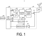
- FIG. 1 is a block diagram illustrating an example of a configuration of the wireless communication apparatus according to an embodiment.
- a wireless communication apparatus 1 includes an antenna 10, a band pass filter (BPF) 11, a radio frequency back scatter (RFBS) device 20, a control device 30, and a sensor 40.
- the wireless communication apparatus 1 is a communication apparatus configured to perform wireless communication of a backscatter system such as an RFID.
- the antenna 10 is configured to receive a signal transmitted to the wireless communication apparatus 1.
- the antenna 10 is configured to transmit a radio wave towards the outside of the wireless communication apparatus 1.
- the BPF 11 is a filter configured to pass a signal in a desired frequency band.
- the RFBS device 20 includes a high frequency switch 21, an amplifier 22, a demodulator 23, an oscillator 24, a low pass filter (LPF) 25, an LPF 26, a control circuit 27, and a transmission circuit 28.
- the RFBS device 20 is a wireless communication device that supports data communication of the backscatter system. In the data communication of the backscatter system, communication is performed using reflection of the transmitted radio wave.
- the high frequency switch 21 is configured to switch connection between the antenna 10 and a transmission circuit system or a reception circuit system.
- the high frequency switch 21 is configured to be able to connect the transmission circuit system to the antenna 10.
- the wireless communication apparatus 1 is configured to transmit when the antenna 10 and the transmission circuit system are connected.
- the high frequency switch 21 is configured to be able to connect the reception circuit system to the antenna 10.
- the transmission circuit system includes the oscillator 24, the LPF 25, the LPF 26, the control circuit 27, and the transmission circuit 28.
- the reception circuit system includes the amplifier 22, the demodulator 23.
- the amplifier 22 is configured to amplify the signal received from the antenna 10 and output the amplified signal.
- the amplifier 22 is configured to output the amplified signal to the demodulator 23.
- the demodulator 23 is configured to execute demodulation processing on an input signal.
- the demodulator 23 is configured to demodulate a signal received from the amplifier 22.
- the demodulator 23 is configured to execute demodulation processing on the signal (modulation signal such as amplitude shift keying (ASK)) received from the amplifier 22.
- ASK amplitude shift keying
- the control device 30 is implemented by, for example, a program stored inside executed by a processor or the like with a random access memory (RAM) or the like as a work area.
- the control device 30 may be a controller.
- the control device 30 may also be implemented by an integrated circuit such as an application specific integrated circuit (ASIC) or a field programmable gate array (FPGA).
- ASIC application specific integrated circuit
- FPGA field programmable gate array
- the control device 30 may be implemented by a combination of software and hardware.
- the control device 30 is configured to output a serial data S1 to the control circuit 27 via the LPF 25.
- the serial data S1 is based on output data from the sensor 40.
- the control device 30 outputs a serial data S2 to the control circuit 27 via the LPF 26.
- the serial data S2 is based on the output data from the sensor 40.
- the serial data S1 has a phase different from the serial data S2 by approximately 90°.
- the control device 30 is configured to output a control signal S3 to the control circuit 27.
- the control signal S3 may be utilized to suppress either the USB signal or the LSB signal with respect to a carrier signal.
- the control device 30 is configured to output a control signal S4 to the oscillator 24.
- the control signal S4 may be utilized to control a channel used for communication.
- the sensor 40 is configured to detect various physical quantities.
- the physical quantities detected by the sensor 40 are not particularly limited.
- the sensor 40 may include, for example, one or both of a temperature sensor configured to detect a temperature around the wireless communication apparatus 1, and an acceleration sensor configured to detect acceleration that is generated in the wireless communication apparatus 1.
- the sensor 40 may include other sensors.
- the oscillator 24 is configured to generate an oscillation signal of a predetermined frequency.
- the oscillator 24 is configured to generate an oscillation signal S5 according to the control signal S4.
- the oscillator 24 is configured to generate an oscillation signal S6 having a phase different from the oscillation signal S5 by 90°.
- the control circuit 27 is configured to control the transmission circuit 28.
- the control circuit 27 is configured to control the transmission circuit 28 to adjust a value of an impedance of the transmission circuit 28 based on the serial data S1, the serial data S2, and the control signal S3.
- the control circuit 27 is configured to change the impedance of the transmission circuit 28. Due to the change in the impedance, a reflection coefficient of an output terminal on the antenna 10 side rotates in a complex plane.
- the control circuit 27 is configured to change the impedance of the transmission circuit 28 to control the reflection coefficient of the output terminal to rotate in the complex plane.
- control circuit 27 is configured to control the impedance of the transmission circuit 28 so as to reduce the USB signal or the LSB signal with respect to the carrier signal in a reflection signal (hereinafter, also referred to as the backscatter signal) to implement the single side band.
- a reflection signal hereinafter, also referred to as the backscatter signal
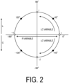
- FIG. 2 is a diagram for describing a method in which the control circuit 27 changes the impedance of the transmission circuit 28 to control the reflection coefficient of the output terminal to rotate.
- FIG. 2 is a diagram illustrating a change in a reflection coefficient ⁇ due to the change in the impedance on the polar chart.
- the impedance is calculated by the following equation (1).
- z is impedance
- R resistance
- j is an imaginary number
- ⁇ is an angular frequency
- L is inductance
- C capacitance.
- Z R + j ⁇ L ⁇ 1 / ⁇ C
- Z 0 is an impedance of the antenna 10 or the BPF 11.
- the control circuit 27 selectively controls the impedance Z to control the reflection coefficient ⁇ so as to rotate around a reference point.
- the reference point includes the origin, but is not limited to the origin and includes any point. The closer to the origin the reference point is, the closer to the ideal signal the transmission circuit can obtain. The more a circumference of the reference point is controlled to circularly rotate, the closer to the ideal signal the transmission circuit can obtain.
- a lower semicircular region indicates a capacitive property
- an upper half indicates an inductive property.
- a change on the real axis represents a change in a resistance value.
- the control circuit 27 can selectively control a plurality of the impedances included in the transmission circuit 28.
- the control circuit 27 is configured to control the impedance of the transmission circuit 28 in 45° increments of 0°, 45°, 90°, 135°, 180°, -135°, -90°, -45°.
- the control circuit 27 is configured to be controllable to discretely rotate the impedance by sequentially changing the impedance of the transmission circuit 28.
- the control circuit 27 discretely rotates the reflection coefficient ⁇ in response to discrete rotation of the impedance.
- the control circuit 27 is configured to be able to change the impedance in counterclockwise rotation by a changing order of the impedance of the transmission circuit 28.
- the control circuit 27 is configured to be able to change the reflection coefficient ⁇ in the counterclockwise rotation by the counterclockwise rotation of the impedance.
- the reflection signal with respect to the radio frequency (RF) is only the upper side band (USB) signal.
- the reflection coefficient is controlled to be clockwise rotation, only the lower side band (LSB) signal is obtained. At that time, the frequency of the reflection signal is detuned from the RF signal frequency by a rotation speed frequency.
- FIG. 3A is a diagram illustrating a frequency spectrum for describing a state of the backscatter signal when the control circuit 27 controls only a resistive component of the impedance, and changes the reflection coefficient ⁇ on the real axis of the polar chart ( FIG. 2 ).
- the horizontal axis represents the frequency
- the vertical axis represents the intensity of the RF signal and the reflection signal.
- a carrier signal 51, a USB signal 52, and an LSB signal 53 are illustrated.
- the reflection coefficient ⁇ is controlled to either 0° or 180° on the real axis.
- the impedance is changed by only the resistive component to control the reflection coefficient ⁇ , as illustrated in FIG.
- the clockwise signal component and the counterclockwise signal component are present in switching from 0° to 180°, for example.
- the signal components in the two rotational directions are present, and thus the USB signal 52 and the LSB signal 53 appear simultaneously, and only one of the signals cannot be selectively suppressed.
- an SSB signal cannot be obtained by controlling only the resistive component.
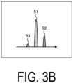
- FIG. 3B is a diagram illustrating a frequency spectrum for describing a change in the backscatter signal when the control circuit 27 changes inductance/capacitance of the impedance to control a trajectory of the reflection coefficient ⁇ so as to form a circle.
- the horizontal axis represents the frequency
- the vertical axis represents the intensity of the RF signal and the reflection signal.
- the control circuit 27 is controllable to rotate the impedance counterclockwise by controlling a value of the inductance. At this time, the impedance is rotated counterclockwise, for example, from 0° to 45°, 90°, and 135°.
- the control circuit 27 is controllable to rotate the impedance counterclockwise by further controlling a value of the capacitance. At this time, the impedance is rotated counterclockwise, for example, from 180° to -135°, -90°, and -45°. As illustrated in FIG. 3B , the control circuit 27 can reflect the transmitted RF signal so as to suppress the LSB signal 53 by controlling the impedance to rotate counterclockwise. In other words, the control circuit 27 can obtain a backscatter signal that is SSB modified to the USB signal 52 by counterclockwise rotation control of the impedance.
- FIG. 3C is a diagram illustrating a frequency spectrum for describing a change in the backscatter signal when the control circuit 27 changes capacitance/inductance of the impedance to control a trajectory of the reflection coefficient ⁇ to form a circle.
- the horizontal axis represents the frequency
- the vertical axis represents the intensity of the RF signal and the reflection signal.
- the control circuit 27 is controllable to rotate the impedance clockwise by controlling the value of the capacitance. At this time, the impedance is rotated clockwise, for example, from 0° to -45°, -90°, and -135°.
- the control circuit 27 is controllable to rotate the impedance clockwise by further controlling the value of the inductance.
- the control circuit 27 can reflect the transmitted RF signal so as to suppress the USB signal 52 by controlling the impedance to rotate clockwise.
- the control circuit 27 can obtain a backscatter signal that is SSB modified to the LSB signal 53 by clockwise rotation control of the impedance.
- the transmission circuit 28 is disposed on a front end of the wireless communication apparatus 1.
- the transmission circuit 28 is a circuit configured to perform backscatter communication in which the transmitted radio wave is reflected as the backscatter signal.
- the transmission circuit 28 is configured to be connected to the antenna 10.
- the transmission circuit 28 includes a plurality of impedance circuits having impedances different from each other.
- Each of the plurality of impedance circuits includes a switch element.
- the switch element is configured to switch a connection of a corresponding impedance circuit.
- the control circuit 27 is configured to control the connection of the plurality of impedance circuits by controlling a plurality of the switch elements.
- the control circuit 27 is configured to control the impedance of the transmission circuit 28 by controlling the plurality of switch elements.
- FIG. 4 is a diagram illustrating an example of the configuration of the transmission circuit according to the first embodiment.
- the transmission circuit 28 includes: inductor circuits 110 1 , 110 2 , and 110 3 ; capacitor circuits 120 1 , 120 2 , and 120 3 ; and a resistive circuit 130.
- Each of the inductor circuits 110 1 to 110 3 , the capacitor circuits 120 1 to 120 3 , and the resistive circuit 130 is a type of the impedance circuit.
- these may be collectively referred to as an inductor circuit 110.
- capacitor circuits 120 1 to 120 3 When it is not necessary to particularly distinguish the capacitor circuits 120 1 to 120 3 from one another, these may be collectively referred to as a capacitor circuit 120.
- FIG. 4 components less relevant to the present disclosure are omitted.
- the inductor circuits 110 1 to 110 3 , the capacitor circuits 120 1 to 120 3 , and the resistive circuit 130 are electrically connected to each other by a signal line 101.
- the signal line 101 is electrically connected to an input/output terminal 102.
- the input/output terminal 102 is electrically connected to a peripheral circuit or the like on the antenna 10 side.
- the inductor circuit 110 1 includes a signal source 140 1 , a switch element 150 1 , and an inductor L1.
- a signal source 140 1 indicates a signal source to which a control signal from the control circuit 27 is supplied.
- the signal source 140 1 is configured to output the control signal to the switch element 150 1 to control an opening/closing operation of the switch element 150 1 .
- the switch element 150 1 includes one input terminal to which the signal source 140 1 is connected and the other input terminal to which a reference potential is connected. The reference potential is described as being the ground, but the present disclosure is not limited thereto.
- the switch element 150 1 is configured to switch between a closed state and an open state in accordance with the control signal from the signal source 140 1 .
- the switch element 150 1 includes one end to which the signal line 101 is electrically connected and the other end to which one end of the inductor L1 is electrically connected. The other end of the inductor L1 is connected to the reference potential. In this case, the switch element 150 1 is configured to electrically connect the signal line 101 and the inductor L1 by being in the closed state. The switch element 150 1 is configured to electrically separate the signal line 101 from the inductor L1 by being in the open state.
- the inductance of the inductor L1 is added to the impedance of the transmission circuit 28 by electrically connecting the signal line 101 and the inductor L1. In other words, a reactance component of the impedance of the transmission circuit 28 changes due to addition of the inductance of the inductor L1.
- the inductance of the inductor L1 is, for example, 3.3 [nano Henry (nH)].
- the inductor circuit 110 2 includes a signal source 140 2 , a switch element 150 2 , and an inductor L2.
- a signal source 140 2 indicates a signal source to which a control signal from the control circuit 27 is supplied.
- the signal source 140 2 is configured to output the control signal to the switch element 150 2 to control an opening/closing operation of the switch element 150 2 .
- the switch element 150 2 includes one input terminal to which the signal source 140 2 is connected and the other input terminal to which the reference potential is connected.
- the reference potential is described as being a ground, but the present disclosure is not limited thereto.
- the switch element 150 2 is configured to switch between the closed state and the open state in accordance with the control signal from the signal source 140 2 .
- the switch element 150 2 includes one end to which the signal line 101 is electrically connected and the other end to which one end of the inductor L2 is electrically connected. The other end of the inductor L2 is connected to the reference potential. In this case, the switch element 150 2 is configured to electrically connect the signal line 101 and the inductor L2 by being in the closed state. The switch element 150 2 is configured to electrically separate the signal line 101 from the inductor L2 by being in the open state.
- the inductance of the inductor L2 is added to the impedance of the transmission circuit 28 by electrically connecting the signal line 101 and the inductor L2. In other words, a reactance component of the impedance of the transmission circuit 28 changes due to addition of the inductance of the inductor L2.
- the inductance of the inductor L2 is, for example, 7.96 [nH].
- the inductor circuit 110 3 includes a signal source 140 3 , a switch element 150 3 , and an inductor L3.
- the signal source 140 3 indicates a signal source to which the control signal from the control circuit 27 is supplied.
- the signal source 140 3 is configured to output the control signal to the switch element 150 3 to control an opening/closing operation of the switch element 150 3 .
- the switch element 150 3 includes one input terminal to which the signal source 140 3 is connected and the other input terminal to which the reference potential is connected. The reference potential is described as being the ground, but the present disclosure is not limited thereto.
- the switch element 150 3 is configured to switch between the closed state and the open state in accordance with the control signal from the signal source 140 3 .
- one or more switch circuits among the inductor circuits 110 1 to 110 3 may include one or more electrical elements from a plurality of capacitor elements and a plurality of resistive elements.
- the switch element 150 3 includes one end to which the signal line 101 is electrically connected and the other end to which one end of the inductor L3 is electrically connected. The other end of the inductor L3 is connected to the reference potential. In this case, the switch element 150 3 is configured to electrically connect the signal line 101 and the inductor L3 by being in the closed state. The switch element 150 3 is configured to electrically separate the signal line 101 from the inductor L3 by being in the open state.
- the inductance of the inductor L3 is added to the impedance of the transmission circuit 28 by electrically connecting the signal line 101 and the inductor L3. In other words, a reactance component of the impedance of the transmission circuit 28 changes due to addition of the inductance of the inductor L3.
- the inductance of the inductor L3 is, for example, 19.21 [nH].
- the capacitor circuit 120 1 includes a signal source 140 4 , a switch element 150 4 , and a capacitor C1.
- the signal source 140 4 indicates a signal source to which the control signal from the control circuit 27 is supplied.
- the signal source 140 4 is configured to output the control signal to the switch element 150 4 to control an opening/closing operation of the switch element 150 4 .
- the switch element 150 4 includes one input terminal to which the signal source 140 4 is connected and the other input terminal to which the reference potential is connected. The reference potential is described as being the ground, but the present disclosure is not limited thereto.
- the switch element 150 4 is configured to switch between the closed state and the open state in accordance with the control signal from the signal source 140 4 .
- the switch element 150 4 includes one end to which the signal line 101 is electrically connected and the other end to which one end of the capacitor C1 is electrically connected. The other end of the capacitor C1 is connected to the reference potential. In this case, the switch element 150 4 is configured to electrically connect the signal line 101 and the capacitor C1 by being in the closed state. The switch element 150 4 is configured to electrically separate the signal line 101 from the capacitor C1 by being in the open state.
- the capacitance of the capacitor C1 is added to the impedance of the transmission circuit 28 by electrically connecting the signal line 101 and the capacitor C1. In other words, a reactance component of the impedance of the transmission circuit 28 changes due to addition of the capacitance of the capacitor C1.
- the capacitance of the capacitor C1 is, for example, 1.32 [pico Farad (pF)].
- the capacitor circuit 120 2 includes a signal source 140 5 , a switch element 150 5 , and a capacitor C2.
- the signal source 140 5 indicates a signal source to which the control signal from the control circuit 27 is supplied.
- the signal source 140 5 is configured to output the control signal to the switch element 150 5 to control an opening/closing operation of the switch element 150 5 .
- the switch element 150 5 includes one input terminal to which the signal source 140 5 is connected and the other input terminal to which the reference potential is connected. The reference potential is described as being the ground, but the present disclosure is not limited thereto.
- the switch element 150 5 is configured to switch between the closed state and the open state in accordance with the control signal from the signal source 140 5 .
- the switch element 150 5 includes one end to which the signal line 101 is electrically connected and the other end to which one end of the capacitor C2 is electrically connected. The other end of the capacitor C2 is connected to the reference potential. In this case, the switch element 150 5 is configured to electrically connect the signal line 101 and the capacitor C2 by being in the closed state. The switch element 150 5 is configured to electrically separate the signal line 101 from the capacitor C2 by being in the open state.
- the capacitance of the capacitor C2 is added to the impedance of the transmission circuit 28 by electrically connecting the signal line 101 and the capacitor C2. In other words, a reactance component of the impedance of the transmission circuit 28 changes due to addition of the capacitance of the capacitor C2.
- the capacitance of the capacitor C2 is, for example, 3.18 [pF].
- the capacitor circuit 120 3 includes a signal source 140 6 , a switch element 150 6 , and a capacitor C3.
- the signal source 140 6 indicates a signal source to which the control signal from the control circuit 27 is supplied.
- the signal source 140 6 is configured to output the control signal to the switch element 150 6 to control an opening/closing operation of the switch element 150 6 .
- the switch element 150 6 includes one input terminal to which the signal source 140 6 is connected and the other input terminal to which the reference potential is connected. The reference potential is described as being the ground, but the present disclosure is not limited thereto.
- the switch element 150 6 is configured to switch between the closed state and the open state in accordance with the control signal from the signal source 140 6 .
- one or more capacitor circuits among the capacitor circuits 120 1 to 120 3 may include one or more electrical elements among a plurality of inductor elements and the plurality of resistive elements.
- the switch element 150 6 includes one end to which the signal line 101 is electrically connected and the other end to which one end of the capacitor C3 is electrically connected. The other end of the capacitor C3 is connected to the reference potential. In this case, the switch element 150 6 is configured to electrically connect the signal line 101 and the capacitor C3 by being in the closed state. The switch element 150 6 is configured to electrically separate the signal line 101 from the capacitor C3 by being in the open state.
- the capacitance of the capacitor C3 is added to the impedance of the transmission circuit 28 by electrically connecting the signal line 101 and the capacitor C3. In other words, a reactance component of the impedance of the transmission circuit 28 changes due to addition of the capacitance of the capacitor C3.
- the capacitance of the capacitor C3 is, for example, 7.68 [pF].
- the resistive circuit 130 includes a signal source 140 7 , a switch element 150 7 , and a resistive element R1.
- the signal source 140 7 indicates a signal source to which the control signal from the control circuit 27 is supplied.
- the signal source 140 7 is configured to output the control signal to the switch element 150 7 to control an opening/closing operation of the switch element 150 7 .
- the switch element 150 7 includes one input terminal to which the signal source 140 7 is connected and the other input terminal to which the reference potential is connected. The reference potential is described as being the ground, but the present disclosure is not limited thereto.
- the switch element 150 7 is configured to switch between the closed state and the open state in accordance with the control signal from the signal source 140 7 .
- the switch element 150 7 includes one end to which the signal line 101 is electrically connected and the other end to which one end of the resistive element R1 is electrically connected. The other end of the resistive element R1 is connected to the reference potential. In this case, the switch element 150 7 is configured to electrically connect the signal line 101 and the resistive element R1 by being in the closed state. The switch element 150 7 is configured to electrically separate the signal line 101 from the resistive element R1 by being in the open state.
- a resistance value of the resistive element R1 is added to the impedance of the transmission circuit 28 by electrically connecting the signal line 101 and the resistive element R1. In other words, the impedance of the transmission circuit 28 changes in the real component by the resistance value of the resistive element R1 being added.
- the resistance value of the resistive element R1 is, for example, 1 [milli-Ohm (mQ)].
- the control circuit 27 is configured to selectively change the impedance of the transmission circuit 28 to control the reflection coefficient to rotate on the polar chart by selectively controlling open/closed state of each of the switch elements 150 1 to 150 7 .
- the control circuit 27 is configured to control the impedance of the transmission circuit 28 to rotate in the complex plane by causing any one of the switch elements 150 1 to 150 7 to be in the closed state or by causing all of the switch elements to be in the open state.
- the control circuit 27 may control the reflection coefficient to rotate by selecting the impedance of the transmission circuit 28 by causing the plurality of switch elements among the switch elements 150 1 to 150 7 to be in the closed state.
- the transmission circuit 28 is configured such that, when all of the switch elements 150 1 to 150 7 are in the open state, the reflection coefficient is located at 0° in the complex plane.
- the transmission circuit 28 is configured such that, when only the switch element 150 3 is in the closed state, the impedance is located at 45° in the complex plane.
- the transmission circuit 28 is configured such that, when only the switch element 150 2 is in the closed state, the impedance is located at 90° in the complex plane.
- the transmission circuit 28 is configured such that, when only the switch element 150 1 is in the closed state, the impedance is located at 135° in the complex plane.
- the transmission circuit 28 is configured such that, when only the switch element 150 4 is in the closed state, the impedance is located at -45° in the complex plane.
- the transmission circuit 28 is configured such that, when only the switch element 150 5 is in the closed state, the impedance is located at -90° in the complex plane.
- the transmission circuit 28 is configured such that, when only the switch element 150 6 is in the closed state, the impedance is located at -135° in the complex plane.
- the transmission circuit 28 is configured such that, when only the switch element 150 7 is in the closed state, the impedance is located at 180° in the complex plane.
- the control circuit 27 may be configured to control the open/closed state of a predetermined switch element(s) among the switch elements 150 1 to 150 7 when reflecting the transmitted radio wave.
- the control circuit 27 may be configured to control the switch elements 150 1 to 150 7 such that the impedance is located at a rotational position in the complex plane, in accordance with output from the sensor 40.
- the control circuit 27 may be configured to control the switch elements 150 1 to 150 7 such that the impedance is located at the rotational position in the complex plane, based on the control signal transmitted from the outside of the wireless communication apparatus 1.
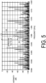
- FIG. 5 illustrates a result example of analyzing the frequency spectrum of the backscatter signal when the reflection coefficient is rotated counterclockwise.
- a spectrum waveform of the backscatter signal (reflection signal) transmitted by the wireless communication apparatus 1 is illustrated.
- the horizontal axis represents frequency
- the vertical axis represents signal intensity.
- a carrier signal 61, a USB signal 62, and an LSB signal 63 are illustrated.
- the frequency of the carrier signal 61 is, for example, 1.0 [Giga Hertz (GHz)].
- the frequency of the USB signal 62 is, for example, 1.001 [GHz].
- the frequency of the LSB signal 63 is, for example, 0.999 [GHz].
- the spectrum intensity of the USB signal 62 is approximately 0 [dB].
- the spectrum intensity of the LSB signal 63 is approximately -60 [dB].
- the difference in spectrum intensity between the USB signal 62 and the LSB signal 63 is -60 [dB].
- the LSB signal 63 is suppressed as compared with the USB signal 62, and thus the single side band of the USB signal 62 is implemented.
- the transmission circuit 28 can implement the single side band by selectively changing the impedance of the transmission circuit 28 to control the reflection coefficient to rotate.
- the transmission circuit 28 can independently utilize both side bands, and improvement of the utilization efficiency of the frequency band can be doubled by controlling the impedance of the transmission circuit 28 so as to suppress either the LSB signal or the USB signal with respect to the carrier signal.
- the transmission circuit 28 can implement the single side band of the backscatter signal without using a configuration such as a demultiplexer.
- the transmission circuit 28 does not require the configuration such as the demultiplexer, and thus the wireless communication apparatus of the backscatter system can be miniaturized.
- the transmission circuit 28 is described as controlling the impedance at eight points in the 45° increments of 0°, 45°, 90°, 135°, 180°, -135°, -90°, and -45° in the complex plane. These angles are exemplary and are not intended to limit the present disclosure.
- the number of points at which the impedance is rotationally controlled is not particularly limited, and may be three, four, six, ten or more.
- the number of points at which the impedance is rotationally controlled is preferably four or more.
- the number of points at which the impedance is rotationally controlled is preferably a multiple of four. In the points at which the impedance is rotationally controlled, angular intervals between points may be the same or different from each other.
- the angular intervals of the points for rotationally controlling the impedance includes not only a case where they exactly match with one another but also a case where they are sifted by a predetermined angle (for example, within 10°).
- a predetermined angle for example, within 10°.
- an angle of a point serving as a reference for rotationally controlling the impedance may be shifted by any angle depending on a design. For example, if it is difficult to control the impedance of the point serving as the reference to 0°, the point may be shifted by about 20°.
- the transmission circuit 28 according to the first embodiment includes the inductor circuit 110, the capacitor circuit 120, and the resistive circuit 130 as the impedance circuit.
- the configuration of the transmission circuit of the present disclosure is not limited thereto.
- the transmission circuit may be configured from the capacitor circuit 120 without including the inductor circuit 110 and the resistive circuit 130.
- the single side band can be implemented using the transmission circuit, a phase shifter that shifts a phase of the signal connected to the transmission circuit by 90°, and the switch element.
- FIG. 6 is a diagram for describing an example of a configuration of the transmission circuit according to the second embodiment.
- the transmission circuit 28A includes the capacitor circuits 120 1 to 120 3 .
- the capacitor circuit 120 1 includes the signal source 140 1 and a switch element 150A 1 ;
- the capacitor circuit 120 2 includes the signal source 140 2 and a switch element 150A 2 ;
- the capacitor circuit 120 3 includes the signal source 140 3 and a switch element 150A 3 .
- switch element 150A is similar to the switch element 150 described in the first embodiment, and thus description thereof is omitted.
- Capacitor circuits 120 1 to 120 3 are electrically connected to one another by a signal line 103.
- the signal line 103 is electrically connected to an input/output terminal 104.
- the capacitor circuits 120 1 to 120 3 are circuits used in rotationally controlling the reflection coefficient clockwise or counterclockwise from -135° to -90° and from -90° to 0°in the complex plane (polar chart).
- the capacitor circuits 120 1 to 120 3 are similar to the capacitor circuits 120 1 to 120 3 , respectively, described in the first embodiment. Specifically, capacitance of the capacitor C1 is 1.32 [pF]. The capacitance of the capacitor C2 is 3.18 [pF]. The capacitance of the capacitor C3 is 7.68 [pF].
- the control circuit 27 can control the impedance of the transmission circuit 28A to rotate in the complex plane by controlling the open/closed state of each of the switch elements 150A 1 to 150A 3 .
- the control circuit 27 is controllable to rotate the impedance of the transmission circuit 28A in the complex plane by causing any one of the switch elements 150A 1 to 150A 3 to be in the closed state or by causing all of the switch elements to be in the open state.
- the control circuit 27 may be controllable to rotate the impedance of the transmission circuit 28A in the complex plane by causing the plurality of switch elements among the switch elements 150A 1 to 150A 3 to be in the open state.
- the transmission circuit 28A When all of the switch elements150A 1 to 150A 3 are in the open state, the transmission circuit 28A is configured such that the impedance is located at 0° in the complex plane. When only the switch element 150A 1 is in the closed state, the transmission circuit 28A is configured such that the impedance is located at -45°. When only the switch element 150A 2 is in the closed state, the transmission circuit 28A is configured such that the impedance is located at -90°. When only the switch element 150A 3 is in the closed state, the transmission circuit 28A is configured such that the impedance is located at -135°. In other words, the control circuit 27 may control the position of the impedance on the complex plane with fourpoint switching by controlling the switch elements 150A 1 to 150A 3 .
- the capacitor circuits 120 1 to 120 3 may be configured to rotationally control the impedance between -135° and -90° and between -90° and 0°.
- the control circuit 27 is configured to rotationally control the impedance of the transmission circuit 28A clockwise by sequentially causing only one of the switch elements 150A 1 , 150A 2 , and 150A 3 to be in the closed state.
- the control circuit 27 is configured to rotationally control the impedance of the transmission circuit 28A counterclockwise by sequentially causing only one of the switch elements 150A 3 , 150A 2 , and 150A 1 to be in the closed state.
- FIG. 7 is a diagram for describing a method of rotationally controlling the reflection coefficient in the complex plane according to the second embodiment ( FIG. 6 ).
- the transmission circuit 28A (the capacitor circuits 120 1 to 120 3 ) illustrated in FIG 6 may be integrated and used as a capacitor IC 160.
- the capacitor IC 160 is configured to be connected to either a phase shifter 170 or a signal line 180 by switching of a changeover switch element 190 by a changeover switch control circuit 200.
- the phase shifter 170 includes a capacitor, an inductor, and a capacitor, which are not illustrated.
- the phase shifter 170 shifts a phase of the input signal by 90° to output the shifted signal.
- the changeover switch control circuit 200 controls the changeover switch element 190 to connect the capacitor IC 160 and the signal line 180 when rotationally controlling the impedance between 0° and -90° and between -90° and -135°.
- the changeover switch control circuit 200 controls the changeover switch element 190 to connect the capacitor IC 160 and the phase shifter 170 when rotationally controlling the impedance between 45° and 90° and between 90° and 180°.
- the position of the impedance on the complex plane can be controlled with eight- point switching by connecting the capacitor IC 160 and the phase shifter 170.
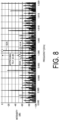
- FIG. 8 illustrates an analysis result of the frequency spectrum of the backscatter signal when the reflection coefficient is rotated counterclockwise.
- a spectrum waveform of the backscatter signal transmitted by the wireless communication apparatus 1 is illustrated.
- a carrier signal 61A, a USB signal 62A, and an LSB signal 63A are illustrated.
- the frequency of the carrier signal 61A is, for example, 1.0 [GHz].
- the frequency of the USB signal 62A is 1.001 [GHz].
- the frequency of the LSB signal 63A is 0.999 [GHz].
- the spectrum intensity of the carrier signal 61A is approximately -50 [dB].
- the spectrum intensity of the USB signal 62 is approximately 0 [dB].
- the spectrum intensity of the LSB signal 63 is approximately -50 [dB].
- the difference in spectrum intensity between the USB signal 62 and the LSB signal 63 is approximately -50 [dB].
- the LSB signal 63 is suppressed as compared with the USB signal 62, and thus the single side band of the USB signal 62 is implemented.
- the use of the inductor having larger size than the resistor and the capacitance can be reduced.
- the configuration is more advantageous for miniaturization.
- phase shifter for shifting the phase is included, but the present disclosure is not limited thereto. In the present disclosure, a plurality of the phase shifters may be included.
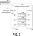
- FIG. 9 is a diagram for describing the configuration of the variation of the second embodiment.
- phase shifter 170A is, for example, a phase shifter configured to shift the phase by 45°.
- the phase shifter 170B is, for example, a phase shifter configured to shift the phase by 90°.
- phase shifter 170C is, for example, a phase shifter configured to shift the phase by 135°.
- the capacitor IC 160 forms IC only for the capacitor circuit 120 1 of the transmission circuit 28A, for example.
- the changeover switch control circuit 200 is configured to control the changeover switch element 190 to connect the capacitor IC 160 and the phase shifter 170A when rotationally controlling the impedance between 0° and 90°.
- the changeover switch control circuit 200 is configured to control the changeover switch element 190 to connect the capacitor IC 160 and the phase shifter 170B when rotationally controlling the impedance between 90° and 180°.
- the changeover switch control circuit 200 is configured to control the changeover switch element 190 to connect the capacitor IC 160 and the phase shifter 170C when rotationally controlling the impedance between 180° and 270°.
- the changeover switch control circuit 200 is configured to control the changeover switch element 190 to connect the capacitor IC 160 and the signal line 180 when rotationally controlling the impedance between 270° and 360°.
- the transmission circuit including the plurality of phase shifters can be configured.
- a modulation processing is performed on the received signal to output the signal.
- the single side band of a modulated signal is implemented in a case where the wireless communication apparatus 1 modulates a signal by using the modulation of, for example, quadrature phase shift keying (QPSK) system.
- QPSK quadrature phase shift keying
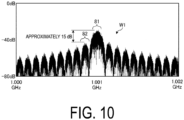
- FIG. 10 is a diagram illustrating the example of the spectrum waveform of the modulation signal.
- FIG. 10 illustrates a spectrum waveform W1 of a QPSK modulated backscatter signal.
- the horizontal axis is frequency
- the vertical axis is intensity.
- the QPSK modulated backscatter signal is a waveform extending in the horizontal axis.
- the difference between a USB signal 81 and a signal 82 adjacent to the USB signal 81 is approximately 15 dB.
- a QPSK modulation system is provided that increases usage efficiency of frequency.
- FIG. 11 is a diagram for describing the QPSK modulation according to the third embodiment.
- FIG. 11 illustrates a signal point arrangement diagram of the QPSK signal according to the third embodiment.
- 16 points of points P1 to P16 are illustrated.
- the phase of the point P1 is 0°.
- the phase of the point P2 is 22.5°.
- the phase of the point P3 is 45°.
- the phase of the point P4 is 67.5°.
- the phase of the point P5 is 90°.
- the phase of the point P6 is 112.5°.
- the phase of the point P7 is 135°.
- the phase of the point P8 is 157.5°.
- the phase of the point P9 is 180°.
- the phase of the point P10 is 202.5°.
- the phase of the point P11 is 225°.
- the point P12 is 247.5°.
- the phase of the point P13 is 270°.
- the phase of the point P14 is 292.5°.
- the phase of the point P15 is 315°.
- the phase of the point P16 is 337.5°.
- Each phase of the points P1 to P16 can be implemented by, for example, an application of a combination (see FIG. 7 ) of the transmission circuit 28A that switches the capacitors with the switches, the phase shifters, and the changeover switches, described in the second embodiment.
- the QPSK modulation four signals whose phases change for each 90° are usually used.
- the point P3 having the phase of 45°, the point P7 having the phase of 135°, the point P11 having the phase of 225°, and the point P15 having the phase of 315° are used.
- the QPSK signal changes from the point P3 to the point P7 in the QPSK modulation, the phase changes rapidly.
- the wireless communication apparatus 1 is configured to continuously change the phase in the QPSK modulation by using the 16 phases illustrated in FIG. 11 .
- the phase of the QPSK signal is controlled to change by 0°, ⁇ 90°, or 180° while one symbol length rotates ten times.
- changing from the point P3 to the point P7 illustrated in FIG. 11 is made via the points P4, P5, P6, and P7, and thus the phase changes with an advance of four times while one symbol length rotates ten times.
- changing from the point P3 to the point P15 is made via the points P2, P1, P16, and P15, and thus the phase changes with a delay of four times.
- the wireless communication apparatus 1 is configured so as to slowly change the phase in the QPSK modulation by using the 16 phases.
- the wireless communication apparatus 1 is configured to be able to quasi-continuously change the phase.
- FIGs. 12 and 13 are diagrams illustrating the examples of the spectrum waveform of the modulation signal according to the third embodiment.
- FIG. 12 illustrates a spectrum waveform W2 when the wireless communication apparatus 1 quasi-continuously advances the phase.
- the difference between a USB signal 83 and a signal 84 adjacent to the USB signal 83 is approximately 30 dB.
- the wireless communication apparatus 1 can increase the utilization efficiency of the frequency by quasi-continuously advancing the phase.
- FIG. 13 illustrates a spectrum waveform W3 when the wireless communication apparatus 1 quasi-continuously delays the phase.
- the difference between a USB signal 85 and a signal 86 adjacent to the USB signal 85 is approximately 30 dB.
- the wireless communication apparatus 1 can increase the utilization efficiency of the frequency by quasi-continuously delaying the phase.
- the wireless communication apparatus 1 can suppress the signal adjacent to the USB signal of the backscatter signal in the QPSK modulation. Accordingly, the wireless communication apparatus 1 can improve the utilization efficiency of the frequency even in the QPSK modulation.
- the method of controlling the reflection coefficient by using the phase modulation is described, but the present disclosure is not limited thereto.
- the reflection coefficient can be also controlled by performing frequency modulation on the SSB signal by changing the rotational speed of the reflection coefficient in accordance with digital information.
Landscapes
- Engineering & Computer Science (AREA)
- Computer Networks & Wireless Communication (AREA)
- Signal Processing (AREA)
- Near-Field Transmission Systems (AREA)
- Transceivers (AREA)
- Transmitters (AREA)
Abstract
Description
- The present disclosure relates to a transmission circuit.
- A backscatter system is known as a data communication method of a wireless communication apparatus. For example,
Patent Document 1 discloses a technique for implementing a single side band by suppressing either an upper side band (USB) signal or a lower side band (LSB) signal by using a demultiplexer/multiplexer. - Patent Document 1:
JP 2005-323223 A - In a radio frequency identification (RFID) system that performs data communication of a backscatter system, miniaturization of a wireless communication apparatus is required. However, in
Patent Document 1, a demultiplexer/multiplexer is used to implement a single side band, and thus a configuration is disadvantageous for miniaturization. - The present disclosure is directed to providing a transmission circuit capable of miniaturizing a wireless communication apparatus of a backscatter system.
- In one aspect of the present disclosure, a transmission circuit is configured to be connected to an antenna. The transmission circuit includes: a plurality of impedance circuits having impedances different from each other; a plurality of first switches, any one of which is being connected to a respective one of the plurality of impedance circuits; a first control circuit configured to control opening and closing of the plurality of first switches. The first control circuit is configured to be controllable to selectively change the opening and closing of the plurality of first switches and to rotate a reflection coefficient of an output terminal on an antenna side of the transmission circuit in a complex plane.
- According to the present disclosure, a wireless communication apparatus of a backscatter system can be miniaturized.
-
-
FIG. 1 is a block diagram illustrating an example of a configuration of a wireless communication apparatus according to a first embodiment. -
FIG. 2 is a diagram for describing a method of rotationally controlling impedance in a complex plane according to the first embodiment. -
FIG. 3A is a diagram for describing a change in a backscatter signal. -
FIG. 3B is a diagram for describing a change in a backscatter signal. -
FIG. 3C is a diagram for describing a change in a backscatter signal. -
FIG. 4 is a diagram illustrating an example of a configuration of a transmission circuit according to the first embodiment. -
FIG. 5 is a diagram illustrating an example of a spectrum waveform of a backscatter signal implementing a single side band according to the first embodiment. -
FIG. 6 is a diagram for describing an example of a configuration of a transmission circuit according to a second embodiment. -
FIG. 7 is a diagram for describing a method of rotationally controlling impedance in a complex plane according to the second embodiment. -
FIG. 8 is a diagram illustrating an example of a spectrum waveform of a backscatter signal implementing a single side band according to the second embodiment. -
FIG. 9 is a diagram for describing a configuration of a variation of the second embodiment. -
FIG. 10 is a diagram illustrating an example of a spectrum waveform of a modulation signal. -
FIG. 11 is a diagram for describing QPSK modulation according to a third embodiment. -
FIG. 12 is a diagram for describing an example of a spectrum waveform of a modulation signal according to the third embodiment. -
FIG. 13 is a diagram illustrating an example of the spectrum waveform of the modulation signal according to the third embodiment. - Embodiments according to the present disclosure will now be described in detail with reference to the accompanying drawings. Note that the present disclosure is not limited by the embodiments, and when there is a plurality of embodiments, the scope of the present disclosure includes a combination of the embodiments. In the following embodiments, the same reference numerals are assigned to the same portions and redundant descriptions thereof will be omitted.
- A configuration of a wireless communication apparatus according to a first embodiment will be described with reference to
FIG. 1. FIG. 1 is a block diagram illustrating an example of a configuration of the wireless communication apparatus according to an embodiment. - As illustrated in
FIG. 1 , awireless communication apparatus 1 includes anantenna 10, a band pass filter (BPF) 11, a radio frequency back scatter (RFBS)device 20, acontrol device 30, and asensor 40. Thewireless communication apparatus 1 is a communication apparatus configured to perform wireless communication of a backscatter system such as an RFID. - The
antenna 10 is configured to receive a signal transmitted to thewireless communication apparatus 1. Theantenna 10 is configured to transmit a radio wave towards the outside of thewireless communication apparatus 1. TheBPF 11 is a filter configured to pass a signal in a desired frequency band. - The
RFBS device 20 includes ahigh frequency switch 21, anamplifier 22, a demodulator 23, anoscillator 24, a low pass filter (LPF) 25, anLPF 26, a control circuit 27, and atransmission circuit 28. TheRFBS device 20 is a wireless communication device that supports data communication of the backscatter system. In the data communication of the backscatter system, communication is performed using reflection of the transmitted radio wave. - The
high frequency switch 21 is configured to switch connection between theantenna 10 and a transmission circuit system or a reception circuit system. Thehigh frequency switch 21 is configured to be able to connect the transmission circuit system to theantenna 10. Thewireless communication apparatus 1 is configured to transmit when theantenna 10 and the transmission circuit system are connected. Thehigh frequency switch 21 is configured to be able to connect the reception circuit system to theantenna 10. The transmission circuit system includes theoscillator 24, the LPF 25, theLPF 26, the control circuit 27, and thetransmission circuit 28. The reception circuit system includes theamplifier 22, the demodulator 23. - The
amplifier 22 is configured to amplify the signal received from theantenna 10 and output the amplified signal. Theamplifier 22 is configured to output the amplified signal to the demodulator 23. The demodulator 23 is configured to execute demodulation processing on an input signal. The demodulator 23 is configured to demodulate a signal received from theamplifier 22. For example, the demodulator 23 is configured to execute demodulation processing on the signal (modulation signal such as amplitude shift keying (ASK)) received from theamplifier 22. - The
control device 30 is implemented by, for example, a program stored inside executed by a processor or the like with a random access memory (RAM) or the like as a work area. Thecontrol device 30 may be a controller. Thecontrol device 30 may also be implemented by an integrated circuit such as an application specific integrated circuit (ASIC) or a field programmable gate array (FPGA). Thecontrol device 30 may be implemented by a combination of software and hardware. - The
control device 30 is configured to output a serial data S1 to the control circuit 27 via the LPF 25. The serial data S1 is based on output data from thesensor 40. Thecontrol device 30 outputs a serial data S2 to the control circuit 27 via theLPF 26. The serial data S2 is based on the output data from thesensor 40. The serial data S1 has a phase different from the serial data S2 by approximately 90°. - The
control device 30 is configured to output a control signal S3 to the control circuit 27. The control signal S3 may be utilized to suppress either the USB signal or the LSB signal with respect to a carrier signal. Thecontrol device 30 is configured to output a control signal S4 to theoscillator 24. The control signal S4 may be utilized to control a channel used for communication. - The
sensor 40 is configured to detect various physical quantities. The physical quantities detected by thesensor 40 are not particularly limited. Thesensor 40 may include, for example, one or both of a temperature sensor configured to detect a temperature around thewireless communication apparatus 1, and an acceleration sensor configured to detect acceleration that is generated in thewireless communication apparatus 1. Thesensor 40 may include other sensors. - The
oscillator 24 is configured to generate an oscillation signal of a predetermined frequency. Theoscillator 24 is configured to generate an oscillation signal S5 according to the control signal S4. Theoscillator 24 is configured to generate an oscillation signal S6 having a phase different from the oscillation signal S5 by 90°. - The control circuit 27 is configured to control the
transmission circuit 28. The control circuit 27 is configured to control thetransmission circuit 28 to adjust a value of an impedance of thetransmission circuit 28 based on the serial data S1, the serial data S2, and the control signal S3. The control circuit 27 is configured to change the impedance of thetransmission circuit 28. Due to the change in the impedance, a reflection coefficient of an output terminal on theantenna 10 side rotates in a complex plane. The control circuit 27 is configured to change the impedance of thetransmission circuit 28 to control the reflection coefficient of the output terminal to rotate in the complex plane. For example, the control circuit 27 is configured to control the impedance of thetransmission circuit 28 so as to reduce the USB signal or the LSB signal with respect to the carrier signal in a reflection signal (hereinafter, also referred to as the backscatter signal) to implement the single side band. - A method will be described by using a polar chart (polar coordinate) in
FIG. 2 , in which the control circuit 27 controls the reflection coefficient of the output terminal on theantenna 10 side of thetransmission circuit 28 so as to rotate on the complex plane of the polar chart.FIG. 2 is a diagram for describing a method in which the control circuit 27 changes the impedance of thetransmission circuit 28 to control the reflection coefficient of the output terminal to rotate. -
FIG. 2 is a diagram illustrating a change in a reflection coefficient Γ due to the change in the impedance on the polar chart. The impedance is calculated by the following equation (1). In the equation (1), z is impedance, R is resistance, j is an imaginary number, ω is an angular frequency, L is inductance, and C is capacitance.
- The reflection coefficient Γ is represented by the following equation.

antenna 10 or theBPF 11. - The control circuit 27 selectively controls the impedance Z to control the reflection coefficient Γ so as to rotate around a reference point. The reference point includes the origin, but is not limited to the origin and includes any point. The closer to the origin the reference point is, the closer to the ideal signal the transmission circuit can obtain. The more a circumference of the reference point is controlled to circularly rotate, the closer to the ideal signal the transmission circuit can obtain. In consideration in a Smith chart, a lower semicircular region indicates a capacitive property, and an upper half indicates an inductive property. A change on the real axis represents a change in a resistance value.
- The control circuit 27 can selectively control a plurality of the impedances included in the
transmission circuit 28. For example, the control circuit 27 is configured to control the impedance of thetransmission circuit 28 in 45° increments of 0°, 45°, 90°, 135°, 180°, -135°, -90°, -45°. The control circuit 27 is configured to be controllable to discretely rotate the impedance by sequentially changing the impedance of thetransmission circuit 28. The control circuit 27 discretely rotates the reflection coefficient Γ in response to discrete rotation of the impedance. - The control circuit 27 is configured to be able to change the impedance in counterclockwise rotation by a changing order of the impedance of the
transmission circuit 28. The control circuit 27 is configured to be able to change the reflection coefficient Γ in the counterclockwise rotation by the counterclockwise rotation of the impedance. When the control of the reflection coefficient is counterclockwise rotation, the reflection signal with respect to the radio frequency (RF) is only the upper side band (USB) signal. When the reflection coefficient is controlled to be clockwise rotation, only the lower side band (LSB) signal is obtained. At that time, the frequency of the reflection signal is detuned from the RF signal frequency by a rotation speed frequency. Several examples of change in the backscatter signal due to change of the impedance to control the reflection coefficient will be described with reference toFIG. 3A ,3B , and3C . -
FIG. 3A is a diagram illustrating a frequency spectrum for describing a state of the backscatter signal when the control circuit 27 controls only a resistive component of the impedance, and changes the reflection coefficient Γ on the real axis of the polar chart (FIG. 2 ). The horizontal axis represents the frequency, and the vertical axis represents the intensity of the RF signal and the reflection signal. InFIG. 3A , acarrier signal 51, aUSB signal 52, and anLSB signal 53 are illustrated. When the resistive component is controlled, the reflection coefficient Γ is controlled to either 0° or 180° on the real axis. When the impedance is changed by only the resistive component to control the reflection coefficient Γ, as illustrated inFIG. 3A , the clockwise signal component and the counterclockwise signal component are present in switching from 0° to 180°, for example. The signal components in the two rotational directions are present, and thus theUSB signal 52 and theLSB signal 53 appear simultaneously, and only one of the signals cannot be selectively suppressed. As a result, an SSB signal cannot be obtained by controlling only the resistive component. -
FIG. 3B is a diagram illustrating a frequency spectrum for describing a change in the backscatter signal when the control circuit 27 changes inductance/capacitance of the impedance to control a trajectory of the reflection coefficient Γ so as to form a circle. The horizontal axis represents the frequency, and the vertical axis represents the intensity of the RF signal and the reflection signal. Based on the equations (1) and (2), the control circuit 27 is controllable to rotate the impedance counterclockwise by controlling a value of the inductance. At this time, the impedance is rotated counterclockwise, for example, from 0° to 45°, 90°, and 135°. The control circuit 27 is controllable to rotate the impedance counterclockwise by further controlling a value of the capacitance. At this time, the impedance is rotated counterclockwise, for example, from 180° to -135°, -90°, and -45°. As illustrated inFIG. 3B , the control circuit 27 can reflect the transmitted RF signal so as to suppress theLSB signal 53 by controlling the impedance to rotate counterclockwise. In other words, the control circuit 27 can obtain a backscatter signal that is SSB modified to theUSB signal 52 by counterclockwise rotation control of the impedance. -
FIG. 3C is a diagram illustrating a frequency spectrum for describing a change in the backscatter signal when the control circuit 27 changes capacitance/inductance of the impedance to control a trajectory of the reflection coefficient Γ to form a circle. The horizontal axis represents the frequency, and the vertical axis represents the intensity of the RF signal and the reflection signal. Based on the equations (1) and (2), the control circuit 27 is controllable to rotate the impedance clockwise by controlling the value of the capacitance. At this time, the impedance is rotated clockwise, for example, from 0° to -45°, -90°, and -135°. The control circuit 27 is controllable to rotate the impedance clockwise by further controlling the value of the inductance. At this time, the impedance is rotated clockwise, for example, to 180°, 135°, 90°, and 45°. As illustrated inFIG. 3C , the control circuit 27 can reflect the transmitted RF signal so as to suppress theUSB signal 52 by controlling the impedance to rotate clockwise. In other words, the control circuit 27 can obtain a backscatter signal that is SSB modified to theLSB signal 53 by clockwise rotation control of the impedance. - The
transmission circuit 28 is disposed on a front end of thewireless communication apparatus 1. Thetransmission circuit 28 is a circuit configured to perform backscatter communication in which the transmitted radio wave is reflected as the backscatter signal. Thetransmission circuit 28 is configured to be connected to theantenna 10. Thetransmission circuit 28 includes a plurality of impedance circuits having impedances different from each other. Each of the plurality of impedance circuits includes a switch element. The switch element is configured to switch a connection of a corresponding impedance circuit. The control circuit 27 is configured to control the connection of the plurality of impedance circuits by controlling a plurality of the switch elements. The control circuit 27 is configured to control the impedance of thetransmission circuit 28 by controlling the plurality of switch elements. - A configuration of the transmission circuit according to the first embodiment will be described with reference to
FIG. 4. FIG. 4 is a diagram illustrating an example of the configuration of the transmission circuit according to the first embodiment. - As illustrated in
FIG. 4 , thetransmission circuit 28 includes:inductor circuits resistive circuit 130. Each of theinductor circuits 1101 to 1103, the capacitor circuits 1201 to 1203, and theresistive circuit 130 is a type of the impedance circuit. When it is not necessary to particularly distinguish theinductor circuits 1101 to 1103 from one another, these may be collectively referred to as aninductor circuit 110. When it is not necessary to particularly distinguish the capacitor circuits 1201 to 1203 from one another, these may be collectively referred to as a capacitor circuit 120. InFIG. 4 , components less relevant to the present disclosure are omitted. - The
inductor circuits 1101 to 1103, the capacitor circuits 1201 to 1203, and theresistive circuit 130 are electrically connected to each other by asignal line 101. Thesignal line 101 is electrically connected to an input/output terminal 102. The input/output terminal 102 is electrically connected to a peripheral circuit or the like on theantenna 10 side. - The
inductor circuit 1101 includes a signal source 1401, a switch element 1501, and an inductor L1. A signal source 1401 indicates a signal source to which a control signal from the control circuit 27 is supplied. The signal source 1401 is configured to output the control signal to the switch element 1501 to control an opening/closing operation of the switch element 1501. The switch element 1501 includes one input terminal to which the signal source 1401 is connected and the other input terminal to which a reference potential is connected. The reference potential is described as being the ground, but the present disclosure is not limited thereto. The switch element 1501 is configured to switch between a closed state and an open state in accordance with the control signal from the signal source 1401. - The switch element 1501 includes one end to which the
signal line 101 is electrically connected and the other end to which one end of the inductor L1 is electrically connected. The other end of the inductor L1 is connected to the reference potential. In this case, the switch element 1501 is configured to electrically connect thesignal line 101 and the inductor L1 by being in the closed state. The switch element 1501 is configured to electrically separate thesignal line 101 from the inductor L1 by being in the open state. The inductance of the inductor L1 is added to the impedance of thetransmission circuit 28 by electrically connecting thesignal line 101 and the inductor L1. In other words, a reactance component of the impedance of thetransmission circuit 28 changes due to addition of the inductance of the inductor L1. The inductance of the inductor L1 is, for example, 3.3 [nano Henry (nH)]. - The
inductor circuit 1102 includes a signal source 1402, a switch element 1502, and an inductor L2. A signal source 1402 indicates a signal source to which a control signal from the control circuit 27 is supplied. The signal source 1402 is configured to output the control signal to the switch element 1502 to control an opening/closing operation of the switch element 1502. The switch element 1502 includes one input terminal to which the signal source 1402 is connected and the other input terminal to which the reference potential is connected. The reference potential is described as being a ground, but the present disclosure is not limited thereto. The switch element 1502 is configured to switch between the closed state and the open state in accordance with the control signal from the signal source 1402. - The switch element 1502 includes one end to which the
signal line 101 is electrically connected and the other end to which one end of the inductor L2 is electrically connected. The other end of the inductor L2 is connected to the reference potential. In this case, the switch element 1502 is configured to electrically connect thesignal line 101 and the inductor L2 by being in the closed state. The switch element 1502 is configured to electrically separate thesignal line 101 from the inductor L2 by being in the open state. The inductance of the inductor L2 is added to the impedance of thetransmission circuit 28 by electrically connecting thesignal line 101 and the inductor L2. In other words, a reactance component of the impedance of thetransmission circuit 28 changes due to addition of the inductance of the inductor L2. The inductance of the inductor L2 is, for example, 7.96 [nH]. - The
inductor circuit 1103 includes a signal source 1403, a switch element 1503, and an inductor L3. The signal source 1403 indicates a signal source to which the control signal from the control circuit 27 is supplied. The signal source 1403 is configured to output the control signal to the switch element 1503 to control an opening/closing operation of the switch element 1503. The switch element 1503 includes one input terminal to which the signal source 1403 is connected and the other input terminal to which the reference potential is connected. The reference potential is described as being the ground, but the present disclosure is not limited thereto. The switch element 1503 is configured to switch between the closed state and the open state in accordance with the control signal from the signal source 1403. Note that one or more switch circuits among theinductor circuits 1101 to 1103 may include one or more electrical elements from a plurality of capacitor elements and a plurality of resistive elements. - The switch element 1503 includes one end to which the
signal line 101 is electrically connected and the other end to which one end of the inductor L3 is electrically connected. The other end of the inductor L3 is connected to the reference potential. In this case, the switch element 1503 is configured to electrically connect thesignal line 101 and the inductor L3 by being in the closed state. The switch element 1503 is configured to electrically separate thesignal line 101 from the inductor L3 by being in the open state. The inductance of the inductor L3 is added to the impedance of thetransmission circuit 28 by electrically connecting thesignal line 101 and the inductor L3. In other words, a reactance component of the impedance of thetransmission circuit 28 changes due to addition of the inductance of the inductor L3. The inductance of the inductor L3 is, for example, 19.21 [nH]. - The capacitor circuit 1201 includes a signal source 1404, a switch element 1504, and a capacitor C1. The signal source 1404 indicates a signal source to which the control signal from the control circuit 27 is supplied. The signal source 1404 is configured to output the control signal to the switch element 1504 to control an opening/closing operation of the switch element 1504. The switch element 1504 includes one input terminal to which the signal source 1404 is connected and the other input terminal to which the reference potential is connected. The reference potential is described as being the ground, but the present disclosure is not limited thereto. The switch element 1504 is configured to switch between the closed state and the open state in accordance with the control signal from the signal source 1404.
- The switch element 1504 includes one end to which the
signal line 101 is electrically connected and the other end to which one end of the capacitor C1 is electrically connected. The other end of the capacitor C1 is connected to the reference potential. In this case, the switch element 1504 is configured to electrically connect thesignal line 101 and the capacitor C1 by being in the closed state. The switch element 1504 is configured to electrically separate thesignal line 101 from the capacitor C1 by being in the open state. The capacitance of the capacitor C1 is added to the impedance of thetransmission circuit 28 by electrically connecting thesignal line 101 and the capacitor C1. In other words, a reactance component of the impedance of thetransmission circuit 28 changes due to addition of the capacitance of the capacitor C1. The capacitance of the capacitor C1 is, for example, 1.32 [pico Farad (pF)]. - The capacitor circuit 1202 includes a signal source 1405, a switch element 1505, and a capacitor C2. The signal source 1405 indicates a signal source to which the control signal from the control circuit 27 is supplied. The signal source 1405 is configured to output the control signal to the switch element 1505 to control an opening/closing operation of the switch element 1505. The switch element 1505 includes one input terminal to which the signal source 1405 is connected and the other input terminal to which the reference potential is connected. The reference potential is described as being the ground, but the present disclosure is not limited thereto. The switch element 1505 is configured to switch between the closed state and the open state in accordance with the control signal from the signal source 1405.
- The switch element 1505 includes one end to which the
signal line 101 is electrically connected and the other end to which one end of the capacitor C2 is electrically connected. The other end of the capacitor C2 is connected to the reference potential. In this case, the switch element 1505 is configured to electrically connect thesignal line 101 and the capacitor C2 by being in the closed state. The switch element 1505 is configured to electrically separate thesignal line 101 from the capacitor C2 by being in the open state. The capacitance of the capacitor C2 is added to the impedance of thetransmission circuit 28 by electrically connecting thesignal line 101 and the capacitor C2. In other words, a reactance component of the impedance of thetransmission circuit 28 changes due to addition of the capacitance of the capacitor C2. The capacitance of the capacitor C2 is, for example, 3.18 [pF]. - The capacitor circuit 1203 includes a signal source 1406, a switch element 1506, and a capacitor C3. The signal source 1406 indicates a signal source to which the control signal from the control circuit 27 is supplied. The signal source 1406 is configured to output the control signal to the switch element 1506 to control an opening/closing operation of the switch element 1506. The switch element 1506 includes one input terminal to which the signal source 1406 is connected and the other input terminal to which the reference potential is connected. The reference potential is described as being the ground, but the present disclosure is not limited thereto. The switch element 1506 is configured to switch between the closed state and the open state in accordance with the control signal from the signal source 1406. Note that one or more capacitor circuits among the capacitor circuits 1201 to 1203 may include one or more electrical elements among a plurality of inductor elements and the plurality of resistive elements.
- The switch element 1506 includes one end to which the
signal line 101 is electrically connected and the other end to which one end of the capacitor C3 is electrically connected. The other end of the capacitor C3 is connected to the reference potential. In this case, the switch element 1506 is configured to electrically connect thesignal line 101 and the capacitor C3 by being in the closed state. The switch element 1506 is configured to electrically separate thesignal line 101 from the capacitor C3 by being in the open state. The capacitance of the capacitor C3 is added to the impedance of thetransmission circuit 28 by electrically connecting thesignal line 101 and the capacitor C3. In other words, a reactance component of the impedance of thetransmission circuit 28 changes due to addition of the capacitance of the capacitor C3. The capacitance of the capacitor C3 is, for example, 7.68 [pF]. - The
resistive circuit 130 includes a signal source 1407, a switch element 1507, and a resistive element R1. The signal source 1407 indicates a signal source to which the control signal from the control circuit 27 is supplied. The signal source 1407 is configured to output the control signal to the switch element 1507 to control an opening/closing operation of the switch element 1507. The switch element 1507 includes one input terminal to which the signal source 1407 is connected and the other input terminal to which the reference potential is connected. The reference potential is described as being the ground, but the present disclosure is not limited thereto. The switch element 1507 is configured to switch between the closed state and the open state in accordance with the control signal from the signal source 1407. - The switch element 1507 includes one end to which the
signal line 101 is electrically connected and the other end to which one end of the resistive element R1 is electrically connected. The other end of the resistive element R1 is connected to the reference potential. In this case, the switch element 1507 is configured to electrically connect thesignal line 101 and the resistive element R1 by being in the closed state. The switch element 1507 is configured to electrically separate thesignal line 101 from the resistive element R1 by being in the open state. A resistance value of the resistive element R1 is added to the impedance of thetransmission circuit 28 by electrically connecting thesignal line 101 and the resistive element R1. In other words, the impedance of thetransmission circuit 28 changes in the real component by the resistance value of the resistive element R1 being added. The resistance value of the resistive element R1 is, for example, 1 [milli-Ohm (mQ)]. - The control circuit 27 is configured to selectively change the impedance of the
transmission circuit 28 to control the reflection coefficient to rotate on the polar chart by selectively controlling open/closed state of each of the switch elements 1501 to 1507. The control circuit 27 is configured to control the impedance of thetransmission circuit 28 to rotate in the complex plane by causing any one of the switch elements 1501 to 1507 to be in the closed state or by causing all of the switch elements to be in the open state. Alternatively, the control circuit 27 may control the reflection coefficient to rotate by selecting the impedance of thetransmission circuit 28 by causing the plurality of switch elements among the switch elements 1501 to 1507 to be in the closed state. - Specifically, the
transmission circuit 28 is configured such that, when all of the switch elements 1501 to 1507 are in the open state, the reflection coefficient is located at 0° in the complex plane. Thetransmission circuit 28 is configured such that, when only the switch element 1503 is in the closed state, the impedance is located at 45° in the complex plane. Thetransmission circuit 28 is configured such that, when only the switch element 1502 is in the closed state, the impedance is located at 90° in the complex plane. Thetransmission circuit 28 is configured such that, when only the switch element 1501 is in the closed state, the impedance is located at 135° in the complex plane. Thetransmission circuit 28 is configured such that, when only the switch element 1504 is in the closed state, the impedance is located at -45° in the complex plane. Thetransmission circuit 28 is configured such that, when only the switch element 1505 is in the closed state, the impedance is located at -90° in the complex plane. Thetransmission circuit 28 is configured such that, when only the switch element 1506 is in the closed state, the impedance is located at -135° in the complex plane. Thetransmission circuit 28 is configured such that, when only the switch element 1507 is in the closed state, the impedance is located at 180° in the complex plane. - The control circuit 27 may be configured to control the open/closed state of a predetermined switch element(s) among the switch elements 1501 to 1507 when reflecting the transmitted radio wave. The control circuit 27 may be configured to control the switch elements 1501 to 1507 such that the impedance is located at a rotational position in the complex plane, in accordance with output from the
sensor 40. The control circuit 27 may be configured to control the switch elements 1501 to 1507 such that the impedance is located at the rotational position in the complex plane, based on the control signal transmitted from the outside of thewireless communication apparatus 1. - A method of implementing the single side band pertaining to the
transmission circuit 28 will be described with reference toFIG. 5 . -
FIG. 5 illustrates a result example of analyzing the frequency spectrum of the backscatter signal when the reflection coefficient is rotated counterclockwise. A spectrum waveform of the backscatter signal (reflection signal) transmitted by thewireless communication apparatus 1 is illustrated. The horizontal axis represents frequency, and the vertical axis represents signal intensity. InFIG. 5 , acarrier signal 61, aUSB signal 62, and anLSB signal 63 are illustrated. The frequency of thecarrier signal 61 is, for example, 1.0 [Giga Hertz (GHz)]. The frequency of theUSB signal 62 is, for example, 1.001 [GHz]. The frequency of theLSB signal 63 is, for example, 0.999 [GHz]. The spectrum intensity of thecarrier signal 61 illustrated inFIG. 5 is approximately -48 [Decibel (dB)]. The spectrum intensity of theUSB signal 62 is approximately 0 [dB]. The spectrum intensity of theLSB signal 63 is approximately -60 [dB]. The difference in spectrum intensity between theUSB signal 62 and theLSB signal 63 is -60 [dB]. In other words, in the spectrum waveform illustrated inFIG. 5 , theLSB signal 63 is suppressed as compared with theUSB signal 62, and thus the single side band of theUSB signal 62 is implemented. - As described above, the
transmission circuit 28 can implement the single side band by selectively changing the impedance of thetransmission circuit 28 to control the reflection coefficient to rotate. In other words, thetransmission circuit 28 can independently utilize both side bands, and improvement of the utilization efficiency of the frequency band can be doubled by controlling the impedance of thetransmission circuit 28 so as to suppress either the LSB signal or the USB signal with respect to the carrier signal. - The
transmission circuit 28 can implement the single side band of the backscatter signal without using a configuration such as a demultiplexer. Thus, thetransmission circuit 28 does not require the configuration such as the demultiplexer, and thus the wireless communication apparatus of the backscatter system can be miniaturized. - Note that the
transmission circuit 28 is described as controlling the impedance at eight points in the 45° increments of 0°, 45°, 90°, 135°, 180°, -135°, -90°, and -45° in the complex plane. These angles are exemplary and are not intended to limit the present disclosure. The number of points at which the impedance is rotationally controlled is not particularly limited, and may be three, four, six, ten or more. The number of points at which the impedance is rotationally controlled is preferably four or more. The number of points at which the impedance is rotationally controlled is preferably a multiple of four. In the points at which the impedance is rotationally controlled, angular intervals between points may be the same or different from each other. In the first embodiment, the angular intervals of the points for rotationally controlling the impedance includes not only a case where they exactly match with one another but also a case where they are sifted by a predetermined angle (for example, within 10°). In the first embodiment, an angle of a point serving as a reference for rotationally controlling the impedance may be shifted by any angle depending on a design. For example, if it is difficult to control the impedance of the point serving as the reference to 0°, the point may be shifted by about 20°. - Next, a transmission circuit according to a second embodiment of the present disclosure will be described. As described above, the
transmission circuit 28 according to the first embodiment includes theinductor circuit 110, the capacitor circuit 120, and theresistive circuit 130 as the impedance circuit. However, the configuration of the transmission circuit of the present disclosure is not limited thereto. For example, the transmission circuit may be configured from the capacitor circuit 120 without including theinductor circuit 110 and theresistive circuit 130. In this case, the single side band can be implemented using the transmission circuit, a phase shifter that shifts a phase of the signal connected to the transmission circuit by 90°, and the switch element. - A configuration of the transmission circuit according to the second embodiment will be described with reference to
FIG. 6. FIG. 6 is a diagram for describing an example of a configuration of the transmission circuit according to the second embodiment. - As illustrated in
FIG. 6 , thetransmission circuit 28A includes the capacitor circuits 1201 to 1203. The capacitor circuit 1201 includes the signal source 1401 and a switch element 150A1; the capacitor circuit 1202 includes the signal source 1402 and a switch element 150A2; the capacitor circuit 1203 includes the signal source 1403 and a switch element 150A3. When it is not necessary to particularly distinguish the switch elements 150A1 to 150A3 from one another, they may be collectively referred to as a switch element 150A. The switch element 150A is similar to the switch element 150 described in the first embodiment, and thus description thereof is omitted. - Capacitor circuits 1201 to 1203 are electrically connected to one another by a
signal line 103. Thesignal line 103 is electrically connected to an input/output terminal 104. The capacitor circuits 1201 to 1203 are circuits used in rotationally controlling the reflection coefficient clockwise or counterclockwise from -135° to -90° and from -90° to 0°in the complex plane (polar chart). - The capacitor circuits 1201 to 1203 are similar to the capacitor circuits 1201 to 1203, respectively, described in the first embodiment. Specifically, capacitance of the capacitor C1 is 1.32 [pF]. The capacitance of the capacitor C2 is 3.18 [pF]. The capacitance of the capacitor C3 is 7.68 [pF].
- The control circuit 27 can control the impedance of the
transmission circuit 28A to rotate in the complex plane by controlling the open/closed state of each of the switch elements 150A1 to 150A3. The control circuit 27 is controllable to rotate the impedance of thetransmission circuit 28A in the complex plane by causing any one of the switch elements 150A1 to 150A3 to be in the closed state or by causing all of the switch elements to be in the open state. The control circuit 27 may be controllable to rotate the impedance of thetransmission circuit 28A in the complex plane by causing the plurality of switch elements among the switch elements 150A1 to 150A3 to be in the open state. - When all of the switch elements150A1 to 150A3 are in the open state, the
transmission circuit 28A is configured such that the impedance is located at 0° in the complex plane. When only the switch element 150A1 is in the closed state, thetransmission circuit 28A is configured such that the impedance is located at -45°. When only the switch element 150A2 is in the closed state, thetransmission circuit 28A is configured such that the impedance is located at -90°. When only the switch element 150A3 is in the closed state, thetransmission circuit 28A is configured such that the impedance is located at -135°. In other words, the control circuit 27 may control the position of the impedance on the complex plane with fourpoint switching by controlling the switch elements 150A1 to 150A3. The capacitor circuits 1201 to 1203 may be configured to rotationally control the impedance between -135° and -90° and between -90° and 0°. The control circuit 27 is configured to rotationally control the impedance of thetransmission circuit 28A clockwise by sequentially causing only one of the switch elements 150A1, 150A2, and 150A3 to be in the closed state. The control circuit 27 is configured to rotationally control the impedance of thetransmission circuit 28A counterclockwise by sequentially causing only one of the switch elements 150A3, 150A2, and 150A1 to be in the closed state. - A method of rotationally controlling the impedance in the complex plane in the transmission circuit according to the second embodiment will be described with reference to
FIG. 7. FIG. 7 is a diagram for describing a method of rotationally controlling the reflection coefficient in the complex plane according to the second embodiment (FIG. 6 ). - As illustrated in
FIG. 7 , thetransmission circuit 28A (the capacitor circuits 1201 to 1203) illustrated inFIG 6 may be integrated and used as acapacitor IC 160. In this case, thecapacitor IC 160 is configured to be connected to either aphase shifter 170 or asignal line 180 by switching of achangeover switch element 190 by a changeoverswitch control circuit 200. - The
phase shifter 170 includes a capacitor, an inductor, and a capacitor, which are not illustrated. Thephase shifter 170 shifts a phase of the input signal by 90° to output the shifted signal. - The changeover
switch control circuit 200 controls thechangeover switch element 190 to connect thecapacitor IC 160 and thesignal line 180 when rotationally controlling the impedance between 0° and -90° and between -90° and -135°. - The changeover
switch control circuit 200 controls thechangeover switch element 190 to connect thecapacitor IC 160 and thephase shifter 170 when rotationally controlling the impedance between 45° and 90° and between 90° and 180°. The position of the impedance on the complex plane can be controlled with eight- point switching by connecting thecapacitor IC 160 and thephase shifter 170. By forming an integrated circuit in this manner, a configuration advantageous for miniaturization can be obtained. - A method of implementing the single side band according to the second embodiment will be described with reference to
FIG. 8 . -
FIG. 8 illustrates an analysis result of the frequency spectrum of the backscatter signal when the reflection coefficient is rotated counterclockwise. A spectrum waveform of the backscatter signal transmitted by thewireless communication apparatus 1 is illustrated. InFIG. 8 , acarrier signal 61A, aUSB signal 62A, and anLSB signal 63A are illustrated. The frequency of thecarrier signal 61A is, for example, 1.0 [GHz]. The frequency of theUSB signal 62A is 1.001 [GHz]. The frequency of theLSB signal 63A is 0.999 [GHz]. The spectrum intensity of thecarrier signal 61A is approximately -50 [dB]. The spectrum intensity of theUSB signal 62 is approximately 0 [dB]. The spectrum intensity of theLSB signal 63 is approximately -50 [dB]. The difference in spectrum intensity between theUSB signal 62 and theLSB signal 63 is approximately -50 [dB]. In other words, in the spectrum waveform illustrated inFIG. 8 , theLSB signal 63 is suppressed as compared with theUSB signal 62, and thus the single side band of theUSB signal 62 is implemented. - In the second embodiment illustrated in
FIG. 7 , the use of the inductor having larger size than the resistor and the capacitance can be reduced. In the second embodiment shown inFIG. 7 , since it is easy to form an IC, the configuration is more advantageous for miniaturization. - Next, a configuration of a variation of the second embodiment according to the present disclosure will be described. In the second embodiment, only one phase shifter for shifting the phase is included, but the present disclosure is not limited thereto. In the present disclosure, a plurality of the phase shifters may be included.
- The configuration of the variation of the second embodiment will be described with reference to
FIG. 9. FIG. 9 is a diagram for describing the configuration of the variation of the second embodiment. - In
FIG. 9 , acapacitor IC 160,phase shifters 170A, 170B, and 170C, and a changeoverswitch control circuit 200 are illustrated. The phase shifter 170A is, for example, a phase shifter configured to shift the phase by 45°. Thephase shifter 170B is, for example, a phase shifter configured to shift the phase by 90°. The phase shifter 170C is, for example, a phase shifter configured to shift the phase by 135°. - In the example illustrated in
FIG. 9 , thecapacitor IC 160 forms IC only for the capacitor circuit 1201 of thetransmission circuit 28A, for example. The changeoverswitch control circuit 200 is configured to control thechangeover switch element 190 to connect thecapacitor IC 160 and the phase shifter 170A when rotationally controlling the impedance between 0° and 90°. The changeoverswitch control circuit 200 is configured to control thechangeover switch element 190 to connect thecapacitor IC 160 and thephase shifter 170B when rotationally controlling the impedance between 90° and 180°. The changeoverswitch control circuit 200 is configured to control thechangeover switch element 190 to connect thecapacitor IC 160 and the phase shifter 170C when rotationally controlling the impedance between 180° and 270°. The changeoverswitch control circuit 200 is configured to control thechangeover switch element 190 to connect thecapacitor IC 160 and thesignal line 180 when rotationally controlling the impedance between 270° and 360°. In the variation of the second embodiment, the transmission circuit including the plurality of phase shifters can be configured. - Next, a third embodiment according to the present disclosure will be described. In the third embodiment, a modulation processing is performed on the received signal to output the signal. In the third embodiment, the single side band of a modulated signal is implemented in a case where the
wireless communication apparatus 1 modulates a signal by using the modulation of, for example, quadrature phase shift keying (QPSK) system. - An example of a spectrum waveform of the modulation signal will be described with reference to
FIG. 10. FIG. 10 is a diagram illustrating the example of the spectrum waveform of the modulation signal. -
FIG. 10 illustrates a spectrum waveform W1 of a QPSK modulated backscatter signal. InFIG. 10 , the horizontal axis is frequency, and the vertical axis is intensity. As illustrated inFIG. 10 , the QPSK modulated backscatter signal is a waveform extending in the horizontal axis. In this case, the difference between aUSB signal 81 and asignal 82 adjacent to theUSB signal 81 is approximately 15 dB. In the third embodiment, a QPSK modulation system is provided that increases usage efficiency of frequency. - The QPSK modulation according to the third embodiment will be described with reference to
FIG. 11. FIG. 11 is a diagram for describing the QPSK modulation according to the third embodiment. -
FIG. 11 illustrates a signal point arrangement diagram of the QPSK signal according to the third embodiment. In the signal point arrangement diagram, 16 points of points P1 to P16 are illustrated. The phase of the point P1 is 0°. The phase of the point P2 is 22.5°. The phase of the point P3 is 45°. The phase of the point P4 is 67.5°. The phase of the point P5 is 90°. The phase of the point P6 is 112.5°. The phase of the point P7 is 135°. The phase of the point P8 is 157.5°. The phase of the point P9 is 180°. The phase of the point P10 is 202.5°. The phase of the point P11 is 225°. The point P12 is 247.5°. The phase of the point P13 is 270°. The phase of the point P14 is 292.5°. The phase of the point P15 is 315°. The phase of the point P16 is 337.5°. Each phase of the points P1 to P16 can be implemented by, for example, an application of a combination (seeFIG. 7 ) of thetransmission circuit 28A that switches the capacitors with the switches, the phase shifters, and the changeover switches, described in the second embodiment. - In the QPSK modulation, four signals whose phases change for each 90° are usually used. In the example illustrated in
FIG. 11 , the point P3 having the phase of 45°, the point P7 having the phase of 135°, the point P11 having the phase of 225°, and the point P15 having the phase of 315° are used. For example, when the QPSK signal changes from the point P3 to the point P7 in the QPSK modulation, the phase changes rapidly. - In the third embodiment, the
wireless communication apparatus 1 is configured to continuously change the phase in the QPSK modulation by using the 16 phases illustrated inFIG. 11 . For example, the phase of the QPSK signal is controlled to change by 0°, ±90°, or 180° while one symbol length rotates ten times. For example, changing from the point P3 to the point P7 illustrated inFIG. 11 is made via the points P4, P5, P6, and P7, and thus the phase changes with an advance of four times while one symbol length rotates ten times. For example, changing from the point P3 to the point P15 is made via the points P2, P1, P16, and P15, and thus the phase changes with a delay of four times. In other words, thewireless communication apparatus 1 is configured so as to slowly change the phase in the QPSK modulation by using the 16 phases. In other words, thewireless communication apparatus 1 is configured to be able to quasi-continuously change the phase. - Examples of a spectrum waveform of the modulation signal according to the third embodiment will be described with reference to
FIGs. 12 and13 .FIGs. 12 and13 are diagrams illustrating the examples of the spectrum waveform of the modulation signal according to the third embodiment. -
FIG. 12 illustrates a spectrum waveform W2 when thewireless communication apparatus 1 quasi-continuously advances the phase. In this case, the difference between aUSB signal 83 and asignal 84 adjacent to theUSB signal 83 is approximately 30 dB. In other words, thewireless communication apparatus 1 can increase the utilization efficiency of the frequency by quasi-continuously advancing the phase. -
FIG. 13 illustrates a spectrum waveform W3 when thewireless communication apparatus 1 quasi-continuously delays the phase. In this case, the difference between aUSB signal 85 and asignal 86 adjacent to theUSB signal 85 is approximately 30 dB. In other words, thewireless communication apparatus 1 can increase the utilization efficiency of the frequency by quasi-continuously delaying the phase. - As described above, in the third embodiment, the
wireless communication apparatus 1 can suppress the signal adjacent to the USB signal of the backscatter signal in the QPSK modulation. Accordingly, thewireless communication apparatus 1 can improve the utilization efficiency of the frequency even in the QPSK modulation. - In the present embodiment, the method of controlling the reflection coefficient by using the phase modulation is described, but the present disclosure is not limited thereto. In the present disclosure, for example, the reflection coefficient can be also controlled by performing frequency modulation on the SSB signal by changing the rotational speed of the reflection coefficient in accordance with digital information.
- The embodiments of the present disclosure have been described above, but the present disclosure is not limited by the contents of these embodiments. The components described above include elements that can be easily conceived by those skilled in the art, elements that are substantially the same, and elements in a so-called equivalent range. Furthermore, the components described above can be combined as appropriate. Furthermore, various omitted, substituted, or modified components can be made without departing from the spirit of the above-described embodiments.
-
- 1 Wireless communication apparatus
- 10 Antenna
- 11 BPF
- 20 RFBS device
- 21 High frequency switch
- 22 Amplifier
- 23 Demodulator
- 24 Oscillator
- 25, 26 LPF
- 27 Control circuit (first control circuit)
- 28 Transmission circuit
- 30 Control device
- 40 Sensor
- 110 Inductor circuit
- 120 Capacitor circuit
- 130 Resistive circuit
- 140 Signal source
- 150, 150A Switch element (first switch element)
- 160 Capacitor IC
- 170, 170A, 170B, 170C Phase shifter
- 190 Changeover switch element (second switch element)
- 200 Changeover switch control circuit (second control circuit)
Claims (19)
- A transmission circuit configured to be connected to an antenna, the transmission circuit comprising:a plurality of impedance circuits having impedances different from each other;a plurality of first switch elements, any one of the plurality of first switch elements being connected to a respective one of the plurality of impedance circuits; anda first control circuit- configured to control opening and closing of the plurality of first switch elements, whereinthe first control circuit is configured to be controllable to selectively change the opening and closing of the plurality of first switch elements and to rotate a reflection coefficient of an output terminal on an antenna side of the transmission circuit in a complex plane.
- The transmission circuit according to claim 1, wherein
the plurality of impedance circuits comprises a plurality of inductor circuits configured to adjust inductance among reactance components of impedance. - The transmission circuit according to claim 2, wherein
the plurality of inductor circuits has impedances different from each other. - The transmission circuit according to claim 2 or 3, wherein
at least one of the plurality of inductor circuits comprises a plurality of inductor elements. - The transmission circuit according to any one of claims 2 to 4, wherein
at least one of the plurality of inductor circuits comprises a resistive element. - The transmission circuit according to any one of claims 2 to 4, wherein
at least one of the plurality of inductor circuits comprises a capacitor element. - The transmission circuit according to any one of claims 1 to 6, wherein
the first control circuit is configured to be controllable to selectively change the opening and closing of the plurality of first switch elements and to rotate impedance at equal interval in the complex plane. - The transmission circuit according to any one of claims 1 to 7, wherein
the plurality of impedance circuits comprises a plurality of capacitor circuits configured to adjust capacitance among reactance components of impedance. - The transmission circuit according to claim 8, wherein
the plurality of capacitor circuits has impedances different from each other. - The transmission circuit according to claim 8 or 9, wherein
at least one of the plurality of capacitor circuits comprises a plurality of capacitor elements. - The transmission circuit according to any one of claims 8 to 10, wherein
at least one of the plurality of capacitor circuits comprises a resistive element. - The transmission circuit according to any one of claims 8 to 10, wherein
at least one of the plurality of capacitor circuits comprises an inductor element. - The transmission circuit according to any one of claims 1 to 12, wherein
the first control circuit is configured to be controllable to change impedance to rotate the reflection coefficient in the complex plane by controlling the plurality of first switch elements to close any one of the plurality of first switch elements. - The transmission circuit according to any one of claims 1 to 12, whereinthe first control circuit is configured to be controllable to change impedance to rotate the reflection coefficient in the complex plane by controlling the plurality of first switch elementsto close any one of the plurality of first switch elements orto open all of the plurality of first switch elements.
- The transmission circuit according to any one of claims 1 to 12, whereinthe first control circuit is configured to be controllable to rotate impedance in the complex plane by controlling the plurality of first switch elementsto close any one of the plurality of first switch elements,to close at least two of the plurality of first switch elements, orto open all of the plurality of first switch elements.
- The transmission circuit according to any one of claims 1 to 12, whereinthe first control circuit is configured to be controllable to rotate impedance in the complex plane by controlling the plurality of first switch elementsto close at least two of the plurality of first switch elements orto open all of the plurality of first switch elements.
- The transmission circuit according to any one of claims 1 to 16, whereinthe transmission circuit comprisesa plurality of phase shifter circuits rotating a phase during transmissiona plurality of second switch elements, any one of the plurality of second switch elements being connected to a respective one of the plurality of phase shifter circuits, anda second control circuit configured to control opening and closing of the plurality of second switch elements, andthe second control circuit is configured to be controllable to change the opening and closing of the plurality of second switch elements, to change impedance, and to rotate a reflection coefficient with respect to the antenna in the complex plane.
- The transmission circuit according to claim 17, wherein
the second control circuit is configured to be controllable to change impedance by closing any one of the plurality of second switch elements and to rotate the reflection coefficient with respect to the antenna in the complex plane. - The transmission circuit according to claim 17 or 18, wherein
the second control circuit is integrated with the first control circuit.
Applications Claiming Priority (2)
| Application Number | Priority Date | Filing Date | Title |
|---|---|---|---|
| JP2020163974A JP7587228B2 (en) | 2020-09-29 | 2020-09-29 | Transmission circuit |
| PCT/JP2021/030870 WO2022070676A1 (en) | 2020-09-29 | 2021-08-23 | Transmission circuit |
Publications (2)
| Publication Number | Publication Date |
|---|---|
| EP4224727A1 true EP4224727A1 (en) | 2023-08-09 |
| EP4224727A4 EP4224727A4 (en) | 2024-11-13 |
Family
ID=80951304
Family Applications (1)
| Application Number | Title | Priority Date | Filing Date |
|---|---|---|---|
| EP21874979.4A Pending EP4224727A4 (en) | 2020-09-29 | 2021-08-23 | TRANSMISSION CIRCUIT |
Country Status (4)
| Country | Link |
|---|---|
| US (1) | US20230361793A1 (en) |
| EP (1) | EP4224727A4 (en) |
| JP (1) | JP7587228B2 (en) |
| WO (1) | WO2022070676A1 (en) |
Cited By (1)
| Publication number | Priority date | Publication date | Assignee | Title |
|---|---|---|---|---|
| EP4485809A4 (en) * | 2022-02-25 | 2026-01-14 | Tokyo Inst Tech | TRANSMISSION CIRCUIT AND COMPOSITE TRANSMISSION CIRCUIT |
Families Citing this family (5)
| Publication number | Priority date | Publication date | Assignee | Title |
|---|---|---|---|---|
| JP7671455B2 (en) * | 2022-02-25 | 2025-05-02 | 国立大学法人東京科学大学 | Transmission circuit |
| JP2025066195A (en) * | 2022-03-11 | 2025-04-23 | 国立大学法人東京科学大学 | Transmission circuit |
| WO2024190732A1 (en) * | 2023-03-13 | 2024-09-19 | 国立大学法人東京工業大学 | Transmission circuit |
| WO2024190844A1 (en) * | 2023-03-15 | 2024-09-19 | 国立大学法人東京工業大学 | Transmission circuit |
| JPWO2024190845A1 (en) * | 2023-03-15 | 2024-09-19 |
Family Cites Families (8)
| Publication number | Priority date | Publication date | Assignee | Title |
|---|---|---|---|---|
| US6816008B2 (en) * | 2002-12-31 | 2004-11-09 | Alion Science And Technology Corporation | Quasi-linear multi-state digital modulation through non-linear amplifier arrays |
| JP4020096B2 (en) | 2004-05-11 | 2007-12-12 | ソニー株式会社 | Wireless communication system, wireless communication apparatus, and wireless communication method |
| JP2009232372A (en) * | 2008-03-25 | 2009-10-08 | Sony Corp | Communication system and communication apparatus |
| EP2330538A1 (en) * | 2009-11-30 | 2011-06-08 | Nxp B.V. | Radio frequency transponder |
| US9306603B2 (en) * | 2014-01-24 | 2016-04-05 | Qualcomm Incorporated | Tunable radio frequency (RF) front-end architecture using filter having adjustable inductance and capacitance |
| US10002266B1 (en) * | 2014-08-08 | 2018-06-19 | Impinj, Inc. | RFID tag clock frequency reduction during tuning |
| US10312885B2 (en) * | 2017-02-15 | 2019-06-04 | Psemi Corporation | Self-matching phase shifter/attenuator |
| US10452968B2 (en) * | 2017-06-14 | 2019-10-22 | Intermec, Inc. | Method to increase RFID tag sensitivity |
-
2020
- 2020-09-29 JP JP2020163974A patent/JP7587228B2/en active Active
-
2021
- 2021-08-23 US US18/245,717 patent/US20230361793A1/en active Pending
- 2021-08-23 EP EP21874979.4A patent/EP4224727A4/en active Pending
- 2021-08-23 WO PCT/JP2021/030870 patent/WO2022070676A1/en not_active Ceased
Cited By (1)
| Publication number | Priority date | Publication date | Assignee | Title |
|---|---|---|---|---|
| EP4485809A4 (en) * | 2022-02-25 | 2026-01-14 | Tokyo Inst Tech | TRANSMISSION CIRCUIT AND COMPOSITE TRANSMISSION CIRCUIT |
Also Published As
| Publication number | Publication date |
|---|---|
| JP2022056139A (en) | 2022-04-08 |
| US20230361793A1 (en) | 2023-11-09 |
| JP7587228B2 (en) | 2024-11-20 |
| EP4224727A4 (en) | 2024-11-13 |
| WO2022070676A1 (en) | 2022-04-07 |
Similar Documents
| Publication | Publication Date | Title |
|---|---|---|
| US20230361793A1 (en) | Transmission circuit | |
| US20230403043A1 (en) | Transmission circuit | |
| EP2037591B1 (en) | Low-IF transceiver architecture | |
| CN107015206B (en) | Adaptive antenna interference detection system and method | |
| RU2115222C1 (en) | Phase-angle corrector for power amplifier feedback circuit (options) | |
| US20230379037A1 (en) | Combiner circuit | |
| US9712313B2 (en) | Systems for multi-peak-filter-based analog self-interference cancellation | |
| EP1424769B1 (en) | Multi-phase mixer circuit and high frequency signal receiver using the same | |
| WO2014062263A1 (en) | Band stitching electronic circuits and techniques | |
| EP4340236A1 (en) | Duplexer architecture using 90 degree hybrid coupler based balancing conditions | |
| US9654150B2 (en) | Module with duplexers coupled to diplexer | |
| US20250150114A1 (en) | Transmission circuit | |
| WO2022175864A1 (en) | Automatic image rejection calibration for radar systems using quadrature transceivers | |
| JP6928509B2 (en) | Power measuring device | |
| CA2955510A1 (en) | System and method for ultra wideband radio frequency scanning and signal generation | |
| EP3771109B1 (en) | Reconfigurable wideband image supressing receiver | |
| EP4485809A1 (en) | Transmission circuit and composite transmission circuit | |
| JP2008072434A (en) | Transmission / reception device and electronic apparatus using the same | |
| US12323123B2 (en) | Phase shifter comprising selectable first and second all-pass filters, where the all-pass filters include capacitors and inductors of determined values to achieve impedance matching | |
| JP3414057B2 (en) | Frequency mixer, transmitting device, receiving device, and transmitting / receiving device | |
| CN106650526B (en) | Phase converter, carrier wave suppression circuit and radio-frequency identification reader/writer | |
| JPH0730463A (en) | Quadrature modulator | |
| JP2006237660A (en) | Antenna device and method of using the same | |
| EP2945296B1 (en) | Spread spectrum communication apparatus | |
| JP7671456B2 (en) | Synthesis Circuit |
Legal Events
| Date | Code | Title | Description |
|---|---|---|---|
| STAA | Information on the status of an ep patent application or granted ep patent |
Free format text: STATUS: THE INTERNATIONAL PUBLICATION HAS BEEN MADE |
|
| PUAI | Public reference made under article 153(3) epc to a published international application that has entered the european phase |
Free format text: ORIGINAL CODE: 0009012 |
|
| STAA | Information on the status of an ep patent application or granted ep patent |
Free format text: STATUS: REQUEST FOR EXAMINATION WAS MADE |
|
| 17P | Request for examination filed |
Effective date: 20230314 |
|
| AK | Designated contracting states |
Kind code of ref document: A1 Designated state(s): AL AT BE BG CH CY CZ DE DK EE ES FI FR GB GR HR HU IE IS IT LI LT LU LV MC MK MT NL NO PL PT RO RS SE SI SK SM TR |
|
| DAV | Request for validation of the european patent (deleted) | ||
| DAX | Request for extension of the european patent (deleted) | ||
| REG | Reference to a national code |
Ref country code: DE Ref legal event code: R079 Free format text: PREVIOUS MAIN CLASS: H04B0005020000 Ipc: G06K0019070000 |
|
| A4 | Supplementary search report drawn up and despatched |
Effective date: 20241016 |
|
| RIC1 | Information provided on ipc code assigned before grant |
Ipc: H04B 1/04 20060101ALI20241010BHEP Ipc: H04B 1/59 20060101ALI20241010BHEP Ipc: G06K 19/07 20060101AFI20241010BHEP |