EP4224534A2 - Solar module - Google Patents
Solar module Download PDFInfo
- Publication number
- EP4224534A2 EP4224534A2 EP22206996.5A EP22206996A EP4224534A2 EP 4224534 A2 EP4224534 A2 EP 4224534A2 EP 22206996 A EP22206996 A EP 22206996A EP 4224534 A2 EP4224534 A2 EP 4224534A2
- Authority
- EP
- European Patent Office
- Prior art keywords
- busbar
- electrode pads
- electrode
- solar
- solar cell
- Prior art date
- Legal status (The legal status is an assumption and is not a legal conclusion. Google has not performed a legal analysis and makes no representation as to the accuracy of the status listed.)
- Pending
Links
Images

Classifications
-
- H—ELECTRICITY
- H10—SEMICONDUCTOR DEVICES; ELECTRIC SOLID-STATE DEVICES NOT OTHERWISE PROVIDED FOR
- H10F—INORGANIC SEMICONDUCTOR DEVICES SENSITIVE TO INFRARED RADIATION, LIGHT, ELECTROMAGNETIC RADIATION OF SHORTER WAVELENGTH OR CORPUSCULAR RADIATION
- H10F19/00—Integrated devices, or assemblies of multiple devices, comprising at least one photovoltaic cell covered by group H10F10/00, e.g. photovoltaic modules
- H10F19/90—Structures for connecting between photovoltaic cells, e.g. interconnections or insulating spacers
- H10F19/902—Structures for connecting between photovoltaic cells, e.g. interconnections or insulating spacers for series or parallel connection of photovoltaic cells
-
- H—ELECTRICITY
- H10—SEMICONDUCTOR DEVICES; ELECTRIC SOLID-STATE DEVICES NOT OTHERWISE PROVIDED FOR
- H10F—INORGANIC SEMICONDUCTOR DEVICES SENSITIVE TO INFRARED RADIATION, LIGHT, ELECTROMAGNETIC RADIATION OF SHORTER WAVELENGTH OR CORPUSCULAR RADIATION
- H10F77/00—Constructional details of devices covered by this subclass
- H10F77/93—Interconnections
- H10F77/933—Interconnections for devices having potential barriers
- H10F77/935—Interconnections for devices having potential barriers for photovoltaic devices or modules
- H10F77/937—Busbar structures for modules
-
- H—ELECTRICITY
- H10—SEMICONDUCTOR DEVICES; ELECTRIC SOLID-STATE DEVICES NOT OTHERWISE PROVIDED FOR
- H10F—INORGANIC SEMICONDUCTOR DEVICES SENSITIVE TO INFRARED RADIATION, LIGHT, ELECTROMAGNETIC RADIATION OF SHORTER WAVELENGTH OR CORPUSCULAR RADIATION
- H10F10/00—Individual photovoltaic cells, e.g. solar cells
- H10F10/10—Individual photovoltaic cells, e.g. solar cells having potential barriers
- H10F10/14—Photovoltaic cells having only PN homojunction potential barriers
-
- H—ELECTRICITY
- H10—SEMICONDUCTOR DEVICES; ELECTRIC SOLID-STATE DEVICES NOT OTHERWISE PROVIDED FOR
- H10F—INORGANIC SEMICONDUCTOR DEVICES SENSITIVE TO INFRARED RADIATION, LIGHT, ELECTROMAGNETIC RADIATION OF SHORTER WAVELENGTH OR CORPUSCULAR RADIATION
- H10F19/00—Integrated devices, or assemblies of multiple devices, comprising at least one photovoltaic cell covered by group H10F10/00, e.g. photovoltaic modules
- H10F19/90—Structures for connecting between photovoltaic cells, e.g. interconnections or insulating spacers
- H10F19/902—Structures for connecting between photovoltaic cells, e.g. interconnections or insulating spacers for series or parallel connection of photovoltaic cells
- H10F19/904—Structures for connecting between photovoltaic cells, e.g. interconnections or insulating spacers for series or parallel connection of photovoltaic cells characterised by the shapes of the structures
-
- H—ELECTRICITY
- H10—SEMICONDUCTOR DEVICES; ELECTRIC SOLID-STATE DEVICES NOT OTHERWISE PROVIDED FOR
- H10F—INORGANIC SEMICONDUCTOR DEVICES SENSITIVE TO INFRARED RADIATION, LIGHT, ELECTROMAGNETIC RADIATION OF SHORTER WAVELENGTH OR CORPUSCULAR RADIATION
- H10F19/00—Integrated devices, or assemblies of multiple devices, comprising at least one photovoltaic cell covered by group H10F10/00, e.g. photovoltaic modules
- H10F19/90—Structures for connecting between photovoltaic cells, e.g. interconnections or insulating spacers
- H10F19/902—Structures for connecting between photovoltaic cells, e.g. interconnections or insulating spacers for series or parallel connection of photovoltaic cells
- H10F19/908—Structures for connecting between photovoltaic cells, e.g. interconnections or insulating spacers for series or parallel connection of photovoltaic cells for back-contact photovoltaic cells
-
- H—ELECTRICITY
- H10—SEMICONDUCTOR DEVICES; ELECTRIC SOLID-STATE DEVICES NOT OTHERWISE PROVIDED FOR
- H10F—INORGANIC SEMICONDUCTOR DEVICES SENSITIVE TO INFRARED RADIATION, LIGHT, ELECTROMAGNETIC RADIATION OF SHORTER WAVELENGTH OR CORPUSCULAR RADIATION
- H10F77/00—Constructional details of devices covered by this subclass
- H10F77/20—Electrodes
- H10F77/206—Electrodes for devices having potential barriers
- H10F77/211—Electrodes for devices having potential barriers for photovoltaic cells
-
- H—ELECTRICITY
- H10—SEMICONDUCTOR DEVICES; ELECTRIC SOLID-STATE DEVICES NOT OTHERWISE PROVIDED FOR
- H10F—INORGANIC SEMICONDUCTOR DEVICES SENSITIVE TO INFRARED RADIATION, LIGHT, ELECTROMAGNETIC RADIATION OF SHORTER WAVELENGTH OR CORPUSCULAR RADIATION
- H10F77/00—Constructional details of devices covered by this subclass
- H10F77/20—Electrodes
- H10F77/206—Electrodes for devices having potential barriers
- H10F77/211—Electrodes for devices having potential barriers for photovoltaic cells
- H10F77/215—Geometries of grid contacts
-
- Y—GENERAL TAGGING OF NEW TECHNOLOGICAL DEVELOPMENTS; GENERAL TAGGING OF CROSS-SECTIONAL TECHNOLOGIES SPANNING OVER SEVERAL SECTIONS OF THE IPC; TECHNICAL SUBJECTS COVERED BY FORMER USPC CROSS-REFERENCE ART COLLECTIONS [XRACs] AND DIGESTS
- Y02—TECHNOLOGIES OR APPLICATIONS FOR MITIGATION OR ADAPTATION AGAINST CLIMATE CHANGE
- Y02E—REDUCTION OF GREENHOUSE GAS [GHG] EMISSIONS, RELATED TO ENERGY GENERATION, TRANSMISSION OR DISTRIBUTION
- Y02E10/00—Energy generation through renewable energy sources
- Y02E10/50—Photovoltaic [PV] energy
Definitions
- the present disclosure relates to the technical field of photovoltaics, and in particular, to a solar module.
- a solar module is a core component of a photovoltaic power generation system, with a function of converting light energy into electric energy.
- the solar module is formed by connecting and encapsulating monolithic solar cells in series.
- the module can obtain a high voltage through series connection, and obtain a high current through parallel connection between multiple strings of solar cells.
- busbars are generally soldered with an electrode line to be corrected in series with the solar cells.
- the electrode line is soldered with electrode pads on the solar cells to play a role of electrical connection.
- the electrode pads on the solar cells may occlude surfaces of photovoltaic cells, which accordingly affects light absorption of the photovoltaic cells and then affects efficiency of the photovoltaic cells.
- the present disclosure provides a solar module, include a solar cells and electrode lines;
- the first electrode pads include first sub-electrode pads and second sub-electrode pads, each of the first sub-electrode pads is located at an end of the busbar, and the second sub-electrode pads are located between the first sub-electrode pads; and each of the first sub-electrode pads has a length ranging from 0.5 mm to 0.8 mm in a direction perpendicular to the electrode line, each of the first sub-electrode pads has a width ranging from 0.5 mm to 1.2 mm in a direction parallel to the electrode line, each of the second sub-electrode pads has a length ranging from 0.05 mm to 0.5 mm in the direction perpendicular to the electrode line, and the second sub-electrode pad has a width ranging from 0.4 mm to 0.8 mm in the direction parallel to the electrode line.
- the diameter of the electrode line ranges from 0.2 mm to 0.33 mm.
- a width of the busbar ranges from 20 ⁇ m to 50 ⁇ m.
- the solar cell substrate is a P-type substrate or an N-type substrate.
- the solar cell substrate is the P-type substrate
- the busbar on the rear surface is provided with second electrode pads, and a number of the second electrode pads ranges from 6 to 12, lengths of the second electrode pads are 1.5 mm, and widths of the second electrode pads range from 2 mm to 3 mm; or
- the solar cell substrate is the N-type substrate
- the busbar on the rear surface is provided with second electrode pads
- a number of the second electrode pads ranges from 10 to 12
- lengths of the second electrode pads ranges from 0.5 mm to 0.8 mm
- widths of the second electrode pads ranges from 0.5 mm to 1.2 mm.
- fingers are provided on the solar cell substrate and intersect with the busbar, and the fingers are electrically connected to the busbar;
- orthographic projections of part of the second electrode pads on a plane of the solar cell substrate do not overlap with orthographic projections of the fingers on the plane of the solar cell substrate.
- a width of the busbar is the same as a width of each of the fingers.
- widths of the fingers range from 20 ⁇ m to 30 ⁇ m; and a number of the fingers ranges from 135 to 150.
- the solar module further includes a first adhesive film material and a second adhesive film material, the solar cells are located between the first adhesive film material and the second adhesive film material, and the first adhesive film material and/or the second adhesive film material has an area density ranging from 310 g/m 2 to 430 g/m 2 .
- each of the first electrode pad has any shape including rectangular shape, diamond shape, circular shape, oval shape, and triangular shape or a combination thereof.
- the solar cells have become commonly used solar energy devices.
- the solar cells may typically be classfied into N-type solar cells and P-type solar cells.
- pure silicon e.g., in the form of heat or light
- several electrons may break off covalent bonds thereof and leave atoms. Each time an electron leaves, a hole is left. Then, the electrons wander around a lattice, looking for another hole to settle in.
- the electrons are called free carriers, which may carry currents. Pure silicon is mixed with phosphorus atoms, and it takes very little energy for an "extra" electron from the phosphorus atoms (outermost five electrons) to escape.
- N-type silicon When phosphorus atoms are used for doping, resulting silicon is called N-type silicon, and the solar cells are only partly N-type. The other part of silicon is doped with boron. Boron has three electrons in the outermost layer instead of four. In this way, P-type silicon can be obtained. P-type silicon has no free electrons.
- Solar cells of an n+/p-type structure formed by diffusing phosphorus on p-type semiconductor materials are P-type silicon wafers.
- Solar cells of a p+/n-type structure formed by injecting boron into N-type semiconductor materials are N-type silicon wafers.
- the N-type solar cells include the N-type silicon wafers, which conduct electricity through electrons, and the P-type solar cells include the P-type silicon wafers, which conduct electricity through holes.
- silver paste is provided on both sides of the N-type solar cells.
- an N-type photovoltaic cell may be a Tunnel Oxide Passivated Contact (TOPCon) solar cell.
- Abase of TOPCon solar cells is an N-type substrate.
- a P-type photovoltaic cell is provided with silver paste on one side and aluminum paste and silver paste on the other side.
- the P-type photovoltaic cell may be a Passivated Emitter and Rear Cell (PERC) solar cell.
- Abase of the PERC solar cell is a P-type substrate.
- the N-type solar cell has higher efficiency, while the P-type solar cell requires a simpler process and lower costs.
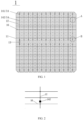
- FIG. 1 is a schematic structural diagram of a front surface of a solar module according to the present disclosure
- FIG. 2 is an enlarged view of A in FIG. 1
- FIG. 3 is an enlarged view of B in FIG. 1
- FIG. 4 is a schematic diagram of a relation between a number busbars and a diameter of an electrode line according to the present disclosure.
- This embodiment provides a solar module, including a plurality of solar cells 1.
- Each of the solar cells 1 includes a solar cell substrate 11 and busbars 12 located on one side of the solar cell substrate 11.
- the solar module further includes an electrode line 13.
- the electrode line 13 has one end connected to the busbar 12 on a front surface of the solar cell sheet 1 and the other end connected to the busbar 12 on a rear surface of the solar cell sheet 1.
- First electrode pads 14 are provided at the busbar, and a number of the first electrode pads 14 ranges from 6 to 12.
- a relation between a diameter of the electrode line 13 and a number of the busbar 12 is 2.987x -1.144 -1.9 ⁇ y ⁇ 3.2742x -1.134 +1.7, where x denotes the diameter of the electrode line, and y denotes the number of the busbar.
- the solar module includes solar cells 1.
- Each of the solar cells 1 includes a solar cell substrate 11 and a plurality of busbars 12 located on one side of the solar cell substrate 11.
- First electrode pads 14 are provided at each of the busbars 12, and a number of the first electrode pads 14 ranges from 6 to 12.
- the solar module further includes an electrode line 13.
- the electrode line 13 is located between adjacent solar cells 1. One end of the electrode line 13 is connected to electrically connected to the first electrode pads 14 at a harpoon of the busbar on the front surface, and the other end of the electrode line 13 is connected to electrically connected to the first electrode pads 14 at a harpoon of the busbar on the rear surface.
- the abscissa is the diameter of the electrode line 13 (in units of mm), and the ordinate is the number of the busbar 12.
- the present disclosure can balance costs and power of the solar module.
- the costs are reduced by reducing the diameter of the electrode line.
- the reduction of the diameter of the electrode line can reduce gram weights of adhesive films without affecting reliability of the module.
- the reduction of the diameter of the electrode line may lead to reduction of a cross-sectional area of current transmission, thereby reducing the power, so there is a need to increase the number of the busbar and the number of the electrode line to increase the power.
- the number of the busbar 12 exceeds a certain value, excessive light may be occluded, and a decrease in the occlusion is greater than an increase in the current transmission, so that the power can be reduced.
- the number of the busbar 12 being within a range of the two can increase the number of the busbar 12, maximize the power of the solar cells, thereby helping to improve conversion efficiency of the photovoltaic cells, minimize gram weights of adhesive films while increasing the power, and reduce the costs.
- the diameter of the electrode line and the number of the busbar of the solar module, the power of the solar module, and the costs of the solar module are studied as follows.
- the maximum power increases first and then decreases, which is an inverted parabola trend.
- the diameter of the electrode line is 0.2
- the power of the solar module increases linearly when the number of the busbar ranges from 9 to 22, while the power of the solar module decreases linearly when the number of the busbar ranges from 23 to 29.
- the diameter of the electrode line is 0.26
- the power of the solar module increases linearly when the number of the busbar ranges from 9 to 16, while the power of the solar module decreases linearly when the number of the busbar ranges from 17 to 29.
- the power of the solar module increases linearly when the number of the busbar ranges from 9 to 13, while the power of the solar module decreases linearly when the number of the busbar ranges from 14 to 29.
- Any diameter of the electrode line between 0.20 mm and 0.33 mm is measured.
- the diameter of the electrode line and the number of the busbar conform to a condition y ⁇ 2.987x -1.144 -1.9, where x denotes the diameter of the electrode line.
- a minimum cost of the solar module can be obtained.
- the diameter of the electrode line is 0.2
- the costs of the solar module decrease linearly when the number of the busbar ranges from 9 to 18, a maximum cost 1.329 of the solar cell is obtained when 18 busbars are provided, and the cost of the solar cell may be increased when 20 busbars are provided.
- the diameter of the electrode line is 0.22
- the costs of the solar module decrease linearly when the number of the busbar ranges from 9 to 16, a maximum cost 1.3251 of the solar cell is obtained, and the cost of the solar cell may be increased when 17 to 20 busbars are provided.
- the diameter of the electrode line is 0.28, the costs of the solar module decrease linearly when 9 to 12 busbars are provided, a maximum cost 1.3314 of the solar cell is obtained, and the cost of the solar cell may be gradually increased when 13 to 20 busbars are provided.
- the diameter of the electrode line is 0.33, a maximum cost 1.3410 of the solar cell is obtained when the number of the busbar is 10, and the cost of the solar cell may be linearly increased when the number of the busbar ranges from 11 to 20. Any diameter of the electrode line between 0.2 mm and 0.33 mm is measured. When all cost values are minimum, the diameter of the electrode line and the number of the busbar conform to a condition y ⁇ 3.2742x -1.134 +1.7, and the value may be rounded down, where x denotes the diameter of the electrode line.
- the formulas of the present disclosure consider the number of the busbar with the maximum efficiency and the number of the busbar with the minimum cost, so a value between the two is taken to ensure that the power is high and the cost is not excessively high. That is, the relation between the diameter of the electrode line 13 and the number of the busbar 12 is 2.987x -1.144 -1.9 ⁇ y ⁇ 3.2742x -1.134 +1.7.
- the number of the busbar 12 can be increased, the power of the solar cells can be maximized, thereby helping to improve conversion efficiency of the photovoltaic cells, gram weights of adhesive films can be reduced while the power is increased, and the costs can be reduced.
- the first electrode pad 14 includes first sub-electrode pads 141 and second sub-electrode pads 142, and the first sub-electrode pads 141 are located at ends of the busbar 12, and the second sub-electrode pads 142 are located between the first sub-electrode pads 141.
- Each of the first sub-electrode pads 141 has a length ranging from 0.5 mm to 0.8 mm perpendicular to the electrode line 13
- the first sub-electrode pad 141 has a width ranging from 0.5 mm to 1.2 mm parallel to the electrode line 13
- each of the second sub-electrode pads 142 has a length ranging from 0.05 mm to 0.5 mm perpendicular to the electrode line 13
- the second sub-electrode pad 142 has a width ranging from 0.4 mm to 0.8 mm parallel to the electrode line 13.
- the first electrode pad 14 includes first sub-electrode pads 141 and second sub-electrode pads 142.
- the first sub-electrode pads 141 may be located at harpoon shapes at two ends of the busbar 12. That is, the first sub-electrode pads 141 may be arranged on two opposite sides of the busbar 12.
- the second sub-electrode pads 142 are located between the first sub-electrode pads 141.
- the busbar 12 is a straight line, so when the first sub-electrode pads 141 are successfully soldered, positions of the busbar 12 and the electrode line 13 are also relatively fixed.
- the solar cells 1 may be applied to a size range of 200 mm to 220 mm.
- the solar cells 1 have lengths and widths that are equal, ranging from 200 mm to 220 mm.
- the solar cells are 210 mm, that is, lengths and widths are 210 mm.
- conventional solar cells of Model 210 are mostly in half, and the busbar 12 is provided with 7 or more electrode pads.
- the number of the second sub-electrode pads 142 in the embodiment of the present disclosure is reduced to 3 compared with an existing solution.
- a spacing between adjacent second sub-electrode pads 142 may range from 18.20 mm to 22.76 mm.
- the first sub-electrode pad 141 has a length ranging from 0.5 mm to 0.8 mm perpendicular to the electrode line 13. In an embodiment, the length of the first sub-electrode pad 141 may be 0.5 mm, 0.6 mm, 0.7 mm, or 0.8 mm.
- the first sub-electrode pad 141 has a width ranging from 0.5 mm to 1.2 mm parallel to the electrode line 13. In an embodiment, the width of the first sub-electrode pad 141 may be 0.5 mm, 0.6 mm, 0.7 mm, 0.8 mm, 0.9 mm, 1.0 mm, or 1.1 mm.
- the length and the widths of the first sub-electrode pad 141 are equal, for example, the length of the first sub-electrode pad 141 and the width of the first sub-electrode pad 141 are both 0.5 mm, so that a contact area between the electrode line 13 and the first sub-electrode pad 141 can be increased, the solar cell sheet 1 can be in better contact with the electrode line 13, soldering tension is increased, and a series soldering machine with high precision positioning is not required. To realize the process, there is a need to flatten the electrode line 13 corresponding to the first sub-electrode pad 141 by drawing the electrode line 13 to the solar cell sheet 1.
- the second sub-electrode pad 142 has a length ranging from 0.05 mm to 0.5 mm perpendicular to the electrode line 13. In an embodiment, the length of the second sub-electrode pad 142 is 0.1 mm, 0.15 mm, 0.2 mm, 0.25 mm, 0.3 mm, 0.35 mm, 0.4 mm, or 0.45 mm.
- the second sub-electrode pad 142 has a width ranging from 0.4 mm to 0.8 mm parallel to the electrode line 13. In an embodiment, the width of the second sub-electrode pad 142 is 0.45 mm, 0.5 mm, 0.55 mm, 0.6 mm, 0.65 mm, 0.7 mm, or 0.75 mm.
- the number and area of the second sub-electrode pad 142 By adjusting the number and area of the second sub-electrode pad 142, occlusion of the second sub-electrode pad 142 to the solar cell substrate 11 can be reduced, thereby helping to reduce the influence of the second sub-electrode pad 142 on light absorption of the solar cell substrate 11 and helping to improve operation efficiency of the photovoltaic cell. At the same time, the area of the second sub-electrode pad 142 is reduced, and silver paste consumed may also be reduced accordingly, thereby helping to reduce the costs.
- the diameter of the electrode line 13 ranges from 0.2 mm to 0.33 mm.
- the diameter of the electrode line 13 may be 0.2 mm, 0.22 mm, 0.24 mm, 0.26 mm, 0.28 mm, 0.3 mm, 0.32 mm, or 0.33 mm.
- the diameter of the electrode line 13 is not specified herein, provided that the diameter ranges from 0.20 mm to 0.33 mm.
- the diameter of the electrode line 13 ranging from 0.2 mm to 0.33 mm can maximize the power of the solar module and minimize the costs of the solar module at the same time.
- a width of the busbar 12 ranges from 20 ⁇ m to 50 ⁇ m.
- the width of the busbar 12 may be 20 ⁇ m, 30 ⁇ m, 40 ⁇ m, 50 ⁇ m, or the like.
- the diameter of the electrode line 13 is reduced by reducing the width of each busbar 12. Therefore, the number and area of the second sub-electrode pads 142 required are also relatively reduced while soldering yield and required soldering tension are ensured, thereby reducing the consumption of silver paste and helping to reduce the costs.
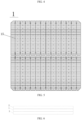
- FIG. 5 is a schematic structural diagram of a rear surface of the solar module according to the present disclosure.
- the solar cell substrate 11 according to this embodiment is the P-type substrate, second electrode pads 15 are provided at the busbar 12 on the rear surface, a number of the second electrode pads 15 ranges from 6 to 12, lengths of the second electrode pads 15 are 1.5 mm, and widths of the second electrode pads 15 range from 2 mm to 3 mm; or the solar cell substrate 11 is the N-type substrate, second electrode pads 15 are provided at the busbar 12 on the rear surface, a number of the second electrode pads 15 ranges from 10 to 12, lengths of the second electrode pads 15 range from 0.5 mm to 0.8 mm, and widths of the second electrode pads 15 range from 0.5 mm to 1.2 mm.
- the solar cell substrate 11 is the P-type substrate
- the second electrode pads 15 are provided at the busbar 12 on the rear surface
- the number of the second electrode pads 15 on the entire P-type substrate ranges from 6 to 12.
- a spacing between adjacent second electrode pads 15 ranges from 18.20 mm to 22.75 mm or from 30.33 mm to 45.50 mm.
- Lengths of the second electrode pads 15 are 1.5 mm
- widths of the second electrode pads 15 range from 2 mm to 3 mm.
- the solar cell substrate 11 is the N-type substrate, the second electrode pads 15 are provided at the busbar 12 on the rear surface, and the number of the second electrode pads 15 on the entire N-type substrate ranges from 10 to 12. Except the second electrode pads 15 at two ends of the busbar 12, a spacing between adjacent second electrode pads 15 ranges from 18.20 mm to 22.76 mm. Lengths of the second electrode pads 15 range from 0.5 mm to 0.8 mm, which are 0.5 mm, 0.6 mm, 0.7 mm, or 0.8 mm for example. Widths of the second electrode pads 15 range from 0.5 mm to 1.2 mm, which are 0.6 mm, 0.7 mm, 0.8 mm, 0.9 mm, 1.0 mm, or 1.1 mm for example. By adjusting the number and area of the second electrode pads 15 on the N-type substrate, the consumption of silver paste can be reduced, and the solar cell sheet 1 can be in better contact with the electrode line 13, thereby increasing soldering tension.
- the solar cell substrate 11 further includes fingers 16 intersecting with the busbar 12.
- the fingers 16 are electrically connected to the busbar 12.
- orthographic projections of part of the second electrode pads 142 on a plane of the solar cell substrate 11 do not overlap with orthographic projections of the fingers 16 on the plane of the solar cell substrate 11.
- the solar cell substrate 11 further includes fingers 16 intersecting with the busbar 12.
- the fingers 16 may be perpendicular to the busbar 12.
- the fingers 16 are electrically connected to the busbar 12.
- the fingers 16 are configured to collect currents generated by the solar cell substrate 11.
- the busbar 12 is configured to collect currents of the fingers 16.
- orthographic projections of part of the second electrode pads 142 on the plane of the solar cell substrate 11 do not overlap with orthographic projections of the fingers 16 on the plane of the solar cell substrate 11. That is, the second electrode pads 142 are arranged on the busbar 12, most of the second electrode pads 142 are not at junctions between the busbar 12 and the fingers 16, and only a small number of the second electrode pads 142 are arranged at the junctions between the busbar 12 and the fingers 16, which reduces electrode breakage at joints between the busbar 12 and the fingers 16 caused by soldering, thereby affecting normal use of the photovoltaic cells.
- a width of the busbar 12 is the same as widths of the fingers 16.
- widths of the fingers 16 range from 20 ⁇ m to 30 ⁇ m, and a number of the fingers 16 ranges from 135 to 150.
- the number of the fingers 16 may be 138, 141, 144, 147, or the like.
- FIG. 6 is another schematic structural diagram of the solar module according to the present disclosure.
- the solar module according to this embodiment further includes a first adhesive film material 2 and a second adhesive film material 3, the solar cells 1 are located between the first adhesive film material 2 and the second adhesive film material 3, and the first adhesive film material 2 and/or the second adhesive film material 3 has an area density ranging from 310 g/m 2 to 430 g/m 2 .
- the first adhesive film material 2 and the second adhesive film material 3 are configured to bond and fix glass and the solar cells 1.
- the reduction of the diameter of the electrode line 13 helps to reduce gram weights of the first adhesive film material 2 and the second adhesive film material 3, so that the first adhesive film material 2 and the second adhesive film material 3 with lower gram weights can be selected when the solar module is packaged, thereby achieving a purpose of reducing packaging costs of the solar module on the premise of ensuring reliability of the solar module.
- the first electrode pad 14 has any shape including rectangular shape, diamond shape, circular shape, oval shape, and triangular shape or a combination thereof.
- the triangular shape can be combined with any one of the rectangular shape, the diamond shape, the circular shape, and the oval shape.
- Such shapes can reduce the area of the first electrode pad 14 compared with a conventional square structure of the electrode pad.
- the design can reduce occlusion of the base, and can also reduce consumption of silver paste and the costs.
- the solar module according to the present disclosure achieves at least the following beneficial effects.
- the present disclosure can balance costs and power of the solar module.
- the costs are reduced by reducing the diameter of the electrode line, because gram weights of the first adhesive film material and the second adhesive film material can be reduced after the diameter of the electrode line is reduced.
- the reduction of the diameter of the electrode line may lead to reduction of a cross-sectional area of current transmission, thereby reducing the power, so there is a need to increase the number of the busbar and the number of the electrode line to increase the power.
- the number of the busbar exceeds a certain value, excessive light may be occluded, and a decrease in the occlusion is greater than an increase in the current transmission, so that the power can be reduced.
- the relation between the diameter of the electrode line and the number of the busbar is set to 2.987x -1.144 -1.9 ⁇ y ⁇ 3.2742x -1.134 +1.7.
- the number of the busbar being within a range of the two can increase the number of the busbar, maximize the power of the solar cells, thereby helping to improve conversion efficiency of the photovoltaic cells, minimize gram weights of adhesive films while increasing the power, and reduce the costs.
Landscapes
- Photovoltaic Devices (AREA)
Abstract
Description
- The present disclosure relates to the technical field of photovoltaics, and in particular, to a solar module.
- A solar module is a core component of a photovoltaic power generation system, with a function of converting light energy into electric energy. The solar module is formed by connecting and encapsulating monolithic solar cells in series. The module can obtain a high voltage through series connection, and obtain a high current through parallel connection between multiple strings of solar cells. In an existing solar module, busbars are generally soldered with an electrode line to be corrected in series with the solar cells. The electrode line is soldered with electrode pads on the solar cells to play a role of electrical connection. However, the electrode pads on the solar cells may occlude surfaces of photovoltaic cells, which accordingly affects light absorption of the photovoltaic cells and then affects efficiency of the photovoltaic cells.
- In view of the above, the present disclosure provides a solar module, include a solar cells and electrode lines;
- each of the solar cells includes a solar cell substrate and busbars located on one side of the solar cell substrate;
- each of the electrode lines has an end connected to the busbar on a front surface of the solar cell and another end connected to the busbar on a rear surface of the solar cell; and
- first electrode pads are provided at the busbar, a number of the first electrode pads ranges from 6 to 12; and a relation between a diameter of the electrode line and a number of the busbar is 2.987x-1.144-1.9<y<3.2742x-1.134+1.7, where x denotes the diameter of the electrode line, and y denotes the number of the busbar.
- In an embodiment, the first electrode pads include first sub-electrode pads and second sub-electrode pads, each of the first sub-electrode pads is located at an end of the busbar, and the second sub-electrode pads are located between the first sub-electrode pads; and
each of the first sub-electrode pads has a length ranging from 0.5 mm to 0.8 mm in a direction perpendicular to the electrode line, each of the first sub-electrode pads has a width ranging from 0.5 mm to 1.2 mm in a direction parallel to the electrode line, each of the second sub-electrode pads has a length ranging from 0.05 mm to 0.5 mm in the direction perpendicular to the electrode line, and the second sub-electrode pad has a width ranging from 0.4 mm to 0.8 mm in the direction parallel to the electrode line. - In an embodiment, the diameter of the electrode line ranges from 0.2 mm to 0.33 mm.
- In an embodiment, a width of the busbar ranges from 20 µm to 50 µm.
- In an embodiment, the solar cell substrate is a P-type substrate or an N-type substrate.
- In an embodiment, the solar cell substrate is the P-type substrate, and the busbar on the rear surface is provided with second electrode pads, and a number of the second electrode pads ranges from 6 to 12, lengths of the second electrode pads are 1.5 mm, and widths of the second electrode pads range from 2 mm to 3 mm; or
- the solar cell substrate is the N-type substrate, and the busbar on the rear surface is provided with second electrode pads, a number of the second electrode pads ranges from 10 to 12, lengths of the second electrode pads ranges from 0.5 mm to 0.8 mm, and widths of the second electrode pads ranges from 0.5 mm to 1.2 mm.
- In an embodiment, fingers are provided on the solar cell substrate and intersect with the busbar, and the fingers are electrically connected to the busbar; and
- in a direction perpendicular to the solar cell substrate, orthographic projections of part of the second electrode pads on a plane of the solar cell substrate do not overlap with orthographic projections of the fingers on the plane of the solar cell substrate.
- In an embodiment, a width of the busbar is the same as a width of each of the fingers.
- In an embodiment, widths of the fingers range from 20 µm to 30 µm; and a number of the fingers ranges from 135 to 150.
- In an embodiment, the solar module further includes a first adhesive film material and a second adhesive film material, the solar cells are located between the first adhesive film material and the second adhesive film material, and the first adhesive film material and/or the second adhesive film material has an area density ranging from 310 g/m2 to 430 g/m2.
- In an embodiment, each of the first electrode pad has any shape including rectangular shape, diamond shape, circular shape, oval shape, and triangular shape or a combination thereof..
- Other features of the present disclosure and advantages thereof will become clear from the following detailed description of exemplary embodiments of the present disclosure with reference to the accompanying drawings.
- The accompanying drawings, which are incorporated in and constitute a part of the specification, illustrate embodiments of the present disclosure and, together with the description, serve to explain the principles of the present disclosure.
-
FIG. 1 is a schematic structural diagram of a front surface of a solar module according to the present disclosure. -
FIG. 2 is an enlarged view of A inFIG. 1 . -
FIG. 3 is an enlarged view of B inFIG. 1 . -
FIG. 4 is a schematic diagram of a relation between a number of busbars and a diameter of an electrode line according to the present disclosure. -
FIG. 5 is a schematic structural diagram of a rear surface of the solar module according to the present disclosure. -
FIG. 6 is another schematic structural diagram of the solar module according to the present disclosure. - Various exemplary embodiments of the present disclosure are now described in detail with reference to the accompanying drawings. It should be noted that, unless otherwise stated specifically, relative arrangement of the components and steps, the numerical expressions, and the values set forth in the embodiments are not intended to limit the scope of the present disclosure.
- The following description of at least one exemplary embodiment is in fact merely illustrative, and in no way constitutes any limitations on the present disclosure and application or use thereof.
- Technologies, methods, and devices known to those of ordinary skill in the related art may not be discussed in detail, but where appropriate, such technologies, methods, and devices should be considered as part of the specification.
- In all the examples shown and discussed herein, any specific value should be construed as merely illustrative and not as a limitation. Therefore, other examples of exemplary embodiments may have different values.
- In some embodiments, similar reference signs and letters denote similar terms in the accompanying drawings, and therefore, once an item is defined in a drawing, there is no need for further discussion in the accompanying drawings.
- With the development of photovoltaic technologies, sizes of solar cells become larger and larger, corresponding currents are higher and higher, and internal losses are also increasing. In order to reduce the losses caused by the currents, the busbar of the solar cells is also gradually increasing. The increase in the busbar can effectively reduce the internal losses. However, when the number of the busbar increases to an extreme value, the power may decrease, because light is excessively occluded and a decrease in the occlusion is greater than an increase in current transmission. At the same time, consumption of silver paste is increased, thereby increasing costs.
- The solar cells have become commonly used solar energy devices. The solar cells may typically be classfied into N-type solar cells and P-type solar cells. When the energy is added to pure silicon (e.g., in the form of heat or light), several electrons may break off covalent bonds thereof and leave atoms. Each time an electron leaves, a hole is left. Then, the electrons wander around a lattice, looking for another hole to settle in. The electrons are called free carriers, which may carry currents. Pure silicon is mixed with phosphorus atoms, and it takes very little energy for an "extra" electron from the phosphorus atoms (outermost five electrons) to escape. When phosphorus atoms are used for doping, resulting silicon is called N-type silicon, and the solar cells are only partly N-type. The other part of silicon is doped with boron. Boron has three electrons in the outermost layer instead of four. In this way, P-type silicon can be obtained. P-type silicon has no free electrons. Solar cells of an n+/p-type structure formed by diffusing phosphorus on p-type semiconductor materials are P-type silicon wafers. Solar cells of a p+/n-type structure formed by injecting boron into N-type semiconductor materials are N-type silicon wafers.
- The N-type solar cells include the N-type silicon wafers, which conduct electricity through electrons, and the P-type solar cells include the P-type silicon wafers, which conduct electricity through holes. In general, silver paste is provided on both sides of the N-type solar cells. In an embodiment, an N-type photovoltaic cell may be a Tunnel Oxide Passivated Contact (TOPCon) solar cell. Abase of TOPCon solar cells is an N-type substrate.
- A P-type photovoltaic cell is provided with silver paste on one side and aluminum paste and silver paste on the other side. In an embodiment, the P-type photovoltaic cell may be a Passivated Emitter and Rear Cell (PERC) solar cell. Abase of the PERC solar cell is a P-type substrate.
- The N-type solar cell has higher efficiency, while the P-type solar cell requires a simpler process and lower costs.
- Referring to
FIG. 1 to FIG. 4 ,FIG. 1 is a schematic structural diagram of a front surface of a solar module according to the present disclosure;FIG. 2 is an enlarged view of A inFIG. 1 ;FIG. 3 is an enlarged view of B inFIG. 1 ; andFIG. 4 is a schematic diagram of a relation between a number busbars and a diameter of an electrode line according to the present disclosure. This embodiment provides a solar module, including a plurality ofsolar cells 1. Each of thesolar cells 1 includes asolar cell substrate 11 andbusbars 12 located on one side of thesolar cell substrate 11. - The solar module further includes an
electrode line 13. Theelectrode line 13 has one end connected to thebusbar 12 on a front surface of thesolar cell sheet 1 and the other end connected to thebusbar 12 on a rear surface of thesolar cell sheet 1. - First electrode pads 14 are provided at the busbar, and a number of the first electrode pads 14 ranges from 6 to 12.
- A relation between a diameter of the
electrode line 13 and a number of thebusbar 12 is 2.987x-1.144-1.9<y<3.2742x-1.134+1.7, where x denotes the diameter of the electrode line, and y denotes the number of the busbar. - In an embodiment, the solar module includes
solar cells 1. Each of thesolar cells 1 includes asolar cell substrate 11 and a plurality ofbusbars 12 located on one side of thesolar cell substrate 11. First electrode pads 14 are provided at each of thebusbars 12, and a number of the first electrode pads 14 ranges from 6 to 12. - The solar module further includes an
electrode line 13. Theelectrode line 13 is located between adjacentsolar cells 1. One end of theelectrode line 13 is connected to electrically connected to the first electrode pads 14 at a harpoon of the busbar on the front surface, and the other end of theelectrode line 13 is connected to electrically connected to the first electrode pads 14 at a harpoon of the busbar on the rear surface. - In
FIG. 4 , the abscissa is the diameter of the electrode line 13 (in units of mm), and the ordinate is the number of thebusbar 12. - The present disclosure can balance costs and power of the solar module. The costs are reduced by reducing the diameter of the electrode line. The reduction of the diameter of the electrode line can reduce gram weights of adhesive films without affecting reliability of the module. However, the reduction of the diameter of the electrode line may lead to reduction of a cross-sectional area of current transmission, thereby reducing the power, so there is a need to increase the number of the busbar and the number of the electrode line to increase the power. However, when the number of the
busbar 12 exceeds a certain value, excessive light may be occluded, and a decrease in the occlusion is greater than an increase in the current transmission, so that the power can be reduced. - In a case that power (in units of W) of 8 to 25
busbars 12 is calculated under the same diameter of theelectrode line 13, an inverted parabola may be obtained, from which the number of thebusbars 12 with maximum power can be obtained. If costs (in units of RMB/W) of the 8 to 25busbars 12 are calculated under the same diameter of theelectrode line 13, a cost extreme value may also be obtained. Therefore, the relation between the diameter of theelectrode line 13 and the number of thebusbar 12 is set to 2.987x-1.144-1.9<y<3.2742x-1.134+1.7, where x denotes the diameter of the electrode line, and y denotes the number of the busbar. The number of thebusbar 12 being within a range of the two can increase the number of thebusbar 12, maximize the power of the solar cells, thereby helping to improve conversion efficiency of the photovoltaic cells, minimize gram weights of adhesive films while increasing the power, and reduce the costs. - In the present disclosure, the diameter of the electrode line and the number of the busbar of the solar module, the power of the solar module, and the costs of the solar module are studied as follows.

- As shown in Table 1, under the same electrode line diameter, as the number of the busbar increases, the maximum power increases first and then decreases, which is an inverted parabola trend. For example, if the diameter of the electrode line is 0.2, the power of the solar module increases linearly when the number of the busbar ranges from 9 to 22, while the power of the solar module decreases linearly when the number of the busbar ranges from 23 to 29. If the diameter of the electrode line is 0.26, the power of the solar module increases linearly when the number of the busbar ranges from 9 to 16, while the power of the solar module decreases linearly when the number of the busbar ranges from 17 to 29. If the diameter of the electrode line is 0.33, the power of the solar module increases linearly when the number of the busbar ranges from 9 to 13, while the power of the solar module decreases linearly when the number of the busbar ranges from 14 to 29. Any diameter of the electrode line between 0.20 mm and 0.33 mm is measured. When the power is maximum, the diameter of the electrode line and the number of the busbar conform to a condition y≈2.987x-1.144-1.9, where x denotes the diameter of the electrode line.

- As can be seen from Table 2, under the same diameter of the electrode line, a minimum cost of the solar module can be obtained. For example, if the diameter of the electrode line is 0.2, the costs of the solar module decrease linearly when the number of the busbar ranges from 9 to 18, a maximum cost 1.329 of the solar cell is obtained when 18 busbars are provided, and the cost of the solar cell may be increased when 20 busbars are provided. If the diameter of the electrode line is 0.22, the costs of the solar module decrease linearly when the number of the busbar ranges from 9 to 16, a maximum cost 1.3251 of the solar cell is obtained, and the cost of the solar cell may be increased when 17 to 20 busbars are provided. If the diameter of the electrode line is 0.28, the costs of the solar module decrease linearly when 9 to 12 busbars are provided, a maximum cost 1.3314 of the solar cell is obtained, and the cost of the solar cell may be gradually increased when 13 to 20 busbars are provided. If the diameter of the electrode line is 0.33, a maximum cost 1.3410 of the solar cell is obtained when the number of the busbar is 10, and the cost of the solar cell may be linearly increased when the number of the busbar ranges from 11 to 20. Any diameter of the electrode line between 0.2 mm and 0.33 mm is measured. When all cost values are minimum, the diameter of the electrode line and the number of the busbar conform to a condition y≈3.2742x-1.134+1.7, and the value may be rounded down, where x denotes the diameter of the electrode line.
- As shown in
FIG. 4 , an optimal number of thebusbar 12 is between a closed pattern enclosed by two lines y=2.987x-1.144-1.9 and y=3.2742x-1.134+1.7. The formulas of the present disclosure consider the number of the busbar with the maximum efficiency and the number of the busbar with the minimum cost, so a value between the two is taken to ensure that the power is high and the cost is not excessively high. That is, the relation between the diameter of theelectrode line 13 and the number of thebusbar 12 is 2.987x-1.144-1.9<y<3.2742x-1.134+1.7. When this condition is satisfied, the number of thebusbar 12 can be increased, the power of the solar cells can be maximized, thereby helping to improve conversion efficiency of the photovoltaic cells, gram weights of adhesive films can be reduced while the power is increased, and the costs can be reduced. - In some embodiments, still referring to
FIG. 1 to FIG. 3 , the first electrode pad 14 includes firstsub-electrode pads 141 and secondsub-electrode pads 142, and the firstsub-electrode pads 141 are located at ends of thebusbar 12, and the secondsub-electrode pads 142 are located between the firstsub-electrode pads 141. - Each of the first
sub-electrode pads 141 has a length ranging from 0.5 mm to 0.8 mm perpendicular to theelectrode line 13, the firstsub-electrode pad 141 has a width ranging from 0.5 mm to 1.2 mm parallel to theelectrode line 13, each of the secondsub-electrode pads 142 has a length ranging from 0.05 mm to 0.5 mm perpendicular to theelectrode line 13, and the secondsub-electrode pad 142 has a width ranging from 0.4 mm to 0.8 mm parallel to theelectrode line 13. - In an embodiment, the first electrode pad 14 includes first
sub-electrode pads 141 and secondsub-electrode pads 142. The firstsub-electrode pads 141 may be located at harpoon shapes at two ends of thebusbar 12. That is, the firstsub-electrode pads 141 may be arranged on two opposite sides of thebusbar 12. The secondsub-electrode pads 142 are located between the firstsub-electrode pads 141. Thebusbar 12 is a straight line, so when the firstsub-electrode pads 141 are successfully soldered, positions of thebusbar 12 and theelectrode line 13 are also relatively fixed. - The
solar cells 1 according to the embodiments of the present disclosure may be applied to a size range of 200 mm to 220 mm. Thesolar cells 1 have lengths and widths that are equal, ranging from 200 mm to 220 mm. In this embodiment, the solar cells are 210 mm, that is, lengths and widths are 210 mm. In general, conventional solar cells of Model 210 are mostly in half, and thebusbar 12 is provided with 7 or more electrode pads. The number of the secondsub-electrode pads 142 in the embodiment of the present disclosure is reduced to 3 compared with an existing solution. A spacing between adjacent secondsub-electrode pads 142 may range from 18.20 mm to 22.76 mm. The firstsub-electrode pad 141 has a length ranging from 0.5 mm to 0.8 mm perpendicular to theelectrode line 13. In an embodiment, the length of the firstsub-electrode pad 141 may be 0.5 mm, 0.6 mm, 0.7 mm, or 0.8 mm. The firstsub-electrode pad 141 has a width ranging from 0.5 mm to 1.2 mm parallel to theelectrode line 13. In an embodiment, the width of the firstsub-electrode pad 141 may be 0.5 mm, 0.6 mm, 0.7 mm, 0.8 mm, 0.9 mm, 1.0 mm, or 1.1 mm. The length and the widths of the firstsub-electrode pad 141 are equal, for example, the length of the firstsub-electrode pad 141 and the width of the firstsub-electrode pad 141 are both 0.5 mm, so that a contact area between theelectrode line 13 and the firstsub-electrode pad 141 can be increased, thesolar cell sheet 1 can be in better contact with theelectrode line 13, soldering tension is increased, and a series soldering machine with high precision positioning is not required. To realize the process, there is a need to flatten theelectrode line 13 corresponding to the firstsub-electrode pad 141 by drawing theelectrode line 13 to thesolar cell sheet 1. - The second
sub-electrode pad 142 has a length ranging from 0.05 mm to 0.5 mm perpendicular to theelectrode line 13. In an embodiment, the length of the secondsub-electrode pad 142 is 0.1 mm, 0.15 mm, 0.2 mm, 0.25 mm, 0.3 mm, 0.35 mm, 0.4 mm, or 0.45 mm. The secondsub-electrode pad 142 has a width ranging from 0.4 mm to 0.8 mm parallel to theelectrode line 13. In an embodiment, the width of the secondsub-electrode pad 142 is 0.45 mm, 0.5 mm, 0.55 mm, 0.6 mm, 0.65 mm, 0.7 mm, or 0.75 mm. By adjusting the number and area of the secondsub-electrode pad 142, occlusion of the secondsub-electrode pad 142 to thesolar cell substrate 11 can be reduced, thereby helping to reduce the influence of the secondsub-electrode pad 142 on light absorption of thesolar cell substrate 11 and helping to improve operation efficiency of the photovoltaic cell. At the same time, the area of the secondsub-electrode pad 142 is reduced, and silver paste consumed may also be reduced accordingly, thereby helping to reduce the costs. - In some embodiments, still referring to
FIG. 4 , the diameter of theelectrode line 13 ranges from 0.2 mm to 0.33 mm. - In an embodiment, the diameter of the
electrode line 13 may be 0.2 mm, 0.22 mm, 0.24 mm, 0.26 mm, 0.28 mm, 0.3 mm, 0.32 mm, or 0.33 mm. The diameter of theelectrode line 13 is not specified herein, provided that the diameter ranges from 0.20 mm to 0.33 mm. The diameter of theelectrode line 13 ranging from 0.2 mm to 0.33 mm can maximize the power of the solar module and minimize the costs of the solar module at the same time. - In some embodiments, still referring to
FIG. 1 , a width of thebusbar 12 ranges from 20 µm to 50 µm. In an embodiment, the width of thebusbar 12 may be 20 µm, 30 µm, 40 µm, 50 µm, or the like. In this embodiment, the diameter of theelectrode line 13 is reduced by reducing the width of eachbusbar 12. Therefore, the number and area of the secondsub-electrode pads 142 required are also relatively reduced while soldering yield and required soldering tension are ensured, thereby reducing the consumption of silver paste and helping to reduce the costs. - In some embodiments, still referring to
FIG. 5, FIG. 5 is a schematic structural diagram of a rear surface of the solar module according to the present disclosure. Thesolar cell substrate 11 according to this embodiment is the P-type substrate,second electrode pads 15 are provided at thebusbar 12 on the rear surface, a number of thesecond electrode pads 15 ranges from 6 to 12, lengths of thesecond electrode pads 15 are 1.5 mm, and widths of thesecond electrode pads 15 range from 2 mm to 3 mm; or
thesolar cell substrate 11 is the N-type substrate,second electrode pads 15 are provided at thebusbar 12 on the rear surface, a number of thesecond electrode pads 15 ranges from 10 to 12, lengths of thesecond electrode pads 15 range from 0.5 mm to 0.8 mm, and widths of thesecond electrode pads 15 range from 0.5 mm to 1.2 mm. - In an embodiment, the
solar cell substrate 11 is the P-type substrate, thesecond electrode pads 15 are provided at thebusbar 12 on the rear surface, and the number of thesecond electrode pads 15 on the entire P-type substrate ranges from 6 to 12. Except thesecond electrode pads 15 at two ends of thebusbar 12, a spacing between adjacentsecond electrode pads 15 ranges from 18.20 mm to 22.75 mm or from 30.33 mm to 45.50 mm. Lengths of thesecond electrode pads 15 are 1.5 mm, and widths of thesecond electrode pads 15 range from 2 mm to 3 mm. By adjusting the number and area of thesecond electrode pads 15 on the P-type substrate, the consumption of silver paste can be reduced, and thesolar cell sheet 1 can be in better contact with theelectrode line 13 to increase soldering tension. - The
solar cell substrate 11 is the N-type substrate, thesecond electrode pads 15 are provided at thebusbar 12 on the rear surface, and the number of thesecond electrode pads 15 on the entire N-type substrate ranges from 10 to 12. Except thesecond electrode pads 15 at two ends of thebusbar 12, a spacing between adjacentsecond electrode pads 15 ranges from 18.20 mm to 22.76 mm. Lengths of thesecond electrode pads 15 range from 0.5 mm to 0.8 mm, which are 0.5 mm, 0.6 mm, 0.7 mm, or 0.8 mm for example. Widths of thesecond electrode pads 15 range from 0.5 mm to 1.2 mm, which are 0.6 mm, 0.7 mm, 0.8 mm, 0.9 mm, 1.0 mm, or 1.1 mm for example. By adjusting the number and area of thesecond electrode pads 15 on the N-type substrate, the consumption of silver paste can be reduced, and thesolar cell sheet 1 can be in better contact with theelectrode line 13, thereby increasing soldering tension. - In some embodiments, still referring to
FIG. 1 and FIG. 2 , thesolar cell substrate 11 further includesfingers 16 intersecting with thebusbar 12. Thefingers 16 are electrically connected to thebusbar 12. - In a direction perpendicular to the
solar cell substrate 11, orthographic projections of part of thesecond electrode pads 142 on a plane of thesolar cell substrate 11 do not overlap with orthographic projections of thefingers 16 on the plane of thesolar cell substrate 11. - In an embodiment, the
solar cell substrate 11 further includesfingers 16 intersecting with thebusbar 12. Thefingers 16 may be perpendicular to thebusbar 12. Thefingers 16 are electrically connected to thebusbar 12. Thefingers 16 are configured to collect currents generated by thesolar cell substrate 11. Thebusbar 12 is configured to collect currents of thefingers 16. - In the direction perpendicular to the
solar cell substrate 11, orthographic projections of part of thesecond electrode pads 142 on the plane of thesolar cell substrate 11 do not overlap with orthographic projections of thefingers 16 on the plane of thesolar cell substrate 11. That is, thesecond electrode pads 142 are arranged on thebusbar 12, most of thesecond electrode pads 142 are not at junctions between thebusbar 12 and thefingers 16, and only a small number of thesecond electrode pads 142 are arranged at the junctions between thebusbar 12 and thefingers 16, which reduces electrode breakage at joints between thebusbar 12 and thefingers 16 caused by soldering, thereby affecting normal use of the photovoltaic cells. - In some embodiments, still referring to
FIG. 1 , a width of thebusbar 12 is the same as widths of thefingers 16. By reducing the width of thebusbar 12, the consumption of silver paste is reduced and conversion efficiency of the module is improved. - In some embodiments, still referring to
FIG. 1 , widths of thefingers 16 range from 20 µm to 30 µm, and a number of thefingers 16 ranges from 135 to 150. For example, the number of thefingers 16 may be 138, 141, 144, 147, or the like. By reducing the number of thefingers 16, the consumption of silver paste and occlusion of electrodes can also be reduced. - In some embodiments, referring to
FIG. 6, FIG. 6 is another schematic structural diagram of the solar module according to the present disclosure. The solar module according to this embodiment further includes a first adhesive film material 2 and a secondadhesive film material 3, thesolar cells 1 are located between the first adhesive film material 2 and the secondadhesive film material 3, and the first adhesive film material 2 and/or the secondadhesive film material 3 has an area density ranging from 310 g/m2 to 430 g/m2. Generally, the first adhesive film material 2 and the secondadhesive film material 3 are configured to bond and fix glass and thesolar cells 1. The reduction of the diameter of theelectrode line 13 helps to reduce gram weights of the first adhesive film material 2 and the secondadhesive film material 3, so that the first adhesive film material 2 and the secondadhesive film material 3 with lower gram weights can be selected when the solar module is packaged, thereby achieving a purpose of reducing packaging costs of the solar module on the premise of ensuring reliability of the solar module. - In some embodiments, still referring to
FIG. 1 andFIG. 4 , the first electrode pad 14 has any shape including rectangular shape, diamond shape, circular shape, oval shape, and triangular shape or a combination thereof.. For example, the triangular shape can be combined with any one of the rectangular shape, the diamond shape, the circular shape, and the oval shape. Such shapes can reduce the area of the first electrode pad 14 compared with a conventional square structure of the electrode pad. The design can reduce occlusion of the base, and can also reduce consumption of silver paste and the costs. - As can be known from the above embodiments, the solar module according to the present disclosure achieves at least the following beneficial effects.
- The present disclosure can balance costs and power of the solar module. The costs are reduced by reducing the diameter of the electrode line, because gram weights of the first adhesive film material and the second adhesive film material can be reduced after the diameter of the electrode line is reduced. However, the reduction of the diameter of the electrode line may lead to reduction of a cross-sectional area of current transmission, thereby reducing the power, so there is a need to increase the number of the busbar and the number of the electrode line to increase the power. However, when the number of the busbar exceeds a certain value, excessive light may be occluded, and a decrease in the occlusion is greater than an increase in the current transmission, so that the power can be reduced. Therefore, the relation between the diameter of the electrode line and the number of the busbar is set to 2.987x-1.144-1.9<y<3.2742x-1.134+1.7. The number of the busbar being within a range of the two can increase the number of the busbar, maximize the power of the solar cells, thereby helping to improve conversion efficiency of the photovoltaic cells, minimize gram weights of adhesive films while increasing the power, and reduce the costs.
- Although some specific embodiments of the present disclosure have been described in detail through examples, it should be understood by those skilled in the art that the above examples are for illustrative purposes only and not intended to limit the scope of the present disclosure. It should be understood by those skilled in the art that the above embodiments can be modified without departing from the scope and spirit of the disclosure. The scope of the present disclosure is defined by the appended claims.
Claims (15)
- A solar module, comprising solar cells and electrode lines; characterized in that,each of the solar cells comprises a solar cell substrate and busbars located on one side of the solar cell substrate;each of the electrode lines has an end connected to the busbar on a front surface of one solar cell sheet of the solar cells and another end connected to the busbar on a rear surface of another solar cell sheet of the solar cells that is adjacent to the one solar cell sheet;first electrode pads are provided at the busbar, a number of the first electrode pads ranges from 6 to 12; anda relation between a diameter of the electrode line and a number of the busbar is
2.987x-1.144-1.9<y<3.2742x-1.134+1.7, where x denotes the diameter of the electrode line, and y denotes the number of the busbar. - The solar module according to claim 1, characterized in that, the first electrode pads comprise first sub-electrode pads and second sub-electrode pads, each of the first sub-electrode pads is located at an end of the busbar, and the second sub-electrode pads are located between the first sub-electrode pads; and
each of the first sub-electrode pads has a length ranging from 0.5 mm to 0.8 mm in a direction perpendicular to the electrode line, each of the first sub-electrode pads has a width ranging from 0.5 mm to 1.2 mm in a direction parallel to the electrode line. - The solar module according to claim 1, characterized in that, the length and the widths of the first sub-electrode pad are equal.
- The solar module according to claim 1, characterized in that, each of the second sub-electrode pads has a length ranging from 0.05 mm to 0.5 mm in the direction perpendicular to the electrode line, and the second sub-electrode pad has a width ranging from 0.4 mm to 0.8 mm in the direction parallel to the electrode line.
- The solar module according to claim 1, characterized in that, the diameter of the electrode line ranges from 0.2 mm to 0.33 mm.
- The solar module according to claim 1, characterized in that, the diameter of the electrode line ranges from 0.22 mm to 0.28 mm.
- The solar module according to claim 1, characterized in that, a width of the busbar ranges from 20 µm to 50 µm.
- The solar module according to claim 1, characterized in that, the solar cell substrate is a P-type substrate or an N-type substrate.
- The solar module according to claim 8, characterized in that, the solar cell substrate is the P-type substrate, and the busbar on the rear surface is provided with second electrode pads, and a number of the second electrode pads ranges from 6 to 12, lengths of the second electrode pads are 1.5 mm, and widths of the second electrode pads range from 2 mm to 3 mm; or
the solar cell substrate is the N-type substrate, and the busbar on the rear surface is provided with second electrode pads, a number of the second electrode pads ranges from 10 to 12, lengths of the second electrode pads ranges from 0.5 mm to 0.8 mm, and widths of the second electrode pads ranges from 0.5 mm to 1.2 mm. - The solar module according to claim 2, characterized in that, fingers are provided on the solar cell substrate and intersect with the busbar, and the fingers are electrically connected to the busbar; and
in a direction perpendicular to the solar cell substrate, orthographic projections of part of the second electrode pads on a plane of the solar cell substrate do not overlap with orthographic projections of the fingers on the plane of the solar cell substrate. - The solar module according to claim 10, characterized in that, a width of the busbar is the same as a width of each of the fingers.
- The solar module according to claim 10, characterized in that,widths of the fingers range from 20 µm to 30 µm; anda number of the fingers ranges from 135 to 150.
- The solar module according to claim 1, characterized in that, the solar module further comprises a first adhesive film material and a second adhesive film material, the solar cells are located between the first adhesive film material and the second adhesive film material, and the first adhesive film material and/or the second adhesive film material has an area density ranging from 310 g/m2 to 430 g/m2.
- The solar module according to claim 1, characterized in that, the solar cells have lengths and widths that are equal, ranging from 200 mm to 220 mm.
- The solar module according to any one of claims 1 to 14, characterized in that, each of the first electrode pads has a shape including rectangular shape, diamond shape, circular shape, oval shape, and triangular shape or a combination thereof.
Applications Claiming Priority (1)
| Application Number | Priority Date | Filing Date | Title |
|---|---|---|---|
| CN202210037606.7A CN115101617B (en) | 2022-01-13 | 2022-01-13 | Solar modules |
Publications (2)
| Publication Number | Publication Date |
|---|---|
| EP4224534A2 true EP4224534A2 (en) | 2023-08-09 |
| EP4224534A3 EP4224534A3 (en) | 2023-11-15 |
Family
ID=83287131
Family Applications (1)
| Application Number | Title | Priority Date | Filing Date |
|---|---|---|---|
| EP22206996.5A Pending EP4224534A3 (en) | 2022-01-13 | 2022-11-11 | Solar module |
Country Status (10)
| Country | Link |
|---|---|
| US (1) | US11949027B2 (en) |
| EP (1) | EP4224534A3 (en) |
| JP (1) | JP7457768B2 (en) |
| CN (1) | CN115101617B (en) |
| AT (1) | AT18044U1 (en) |
| AU (2) | AU2022268276B2 (en) |
| DE (1) | DE202023100012U1 (en) |
| FR (1) | FR3131803B3 (en) |
| GB (1) | GB2614808A (en) |
| NL (1) | NL2033600B1 (en) |
Families Citing this family (3)
| Publication number | Priority date | Publication date | Assignee | Title |
|---|---|---|---|---|
| US20240395956A1 (en) * | 2023-05-23 | 2024-11-28 | Zhejiang Jinko Solar Co., Ltd. | Solar cell, photovoltaic module, and method for manufacturing a silicon substrate |
| CN117199146A (en) * | 2023-11-07 | 2023-12-08 | 晶科能源(海宁)有限公司 | Solar cells and preparation methods thereof, photovoltaic modules |
| CN118983356B (en) * | 2024-08-02 | 2026-02-06 | 晶科能源股份有限公司 | Photovoltaic cell and photovoltaic module |
Family Cites Families (34)
| Publication number | Priority date | Publication date | Assignee | Title |
|---|---|---|---|---|
| JPS6242468A (en) * | 1985-08-19 | 1987-02-24 | Sharp Corp | Electrical connection method for solar cell |
| JPH11243224A (en) * | 1997-12-26 | 1999-09-07 | Canon Inc | Photovoltaic element module, method of manufacturing the same, and non-contact processing method |
| JP5938665B2 (en) * | 2012-07-31 | 2016-06-22 | パナソニックIpマネジメント株式会社 | Manufacturing method of solar cell module |
| US20140124014A1 (en) * | 2012-11-08 | 2014-05-08 | Cogenra Solar, Inc. | High efficiency configuration for solar cell string |
| JP6273583B2 (en) * | 2012-11-30 | 2018-02-07 | パナソニックIpマネジメント株式会社 | Solar cell |
| JP6221554B2 (en) * | 2013-09-20 | 2017-11-01 | 日本電気株式会社 | Joining structure and joining method, metal lead |
| EP3410493B1 (en) | 2014-06-26 | 2020-06-24 | Lg Electronics Inc. | Solar cell module |
| EP3373341B1 (en) * | 2014-09-30 | 2019-09-18 | LG Electronics Inc. | Solar cell |
| KR101820103B1 (en) | 2014-10-27 | 2018-01-18 | 엘지전자 주식회사 | Solar cell module and Methods and Apparatus thereof |
| CN204885175U (en) * | 2015-04-30 | 2015-12-16 | 比亚迪股份有限公司 | Solar cell array, solar cell module |
| JP2018125317A (en) * | 2015-06-04 | 2018-08-09 | 株式会社ブリヂストン | Solar cell sealing film and solar cell module |
| KR101739404B1 (en) | 2015-08-07 | 2017-06-08 | 엘지전자 주식회사 | Solar cell panel |
| JPWO2017179523A1 (en) * | 2016-04-14 | 2019-02-21 | 株式会社カネカ | Solar cell wiring material and solar cell module |
| CN106229356A (en) * | 2016-08-31 | 2016-12-14 | 连云港神舟新能源有限公司 | A kind of many main grids double-side solar cell assembly |
| WO2018070636A1 (en) | 2016-10-13 | 2018-04-19 | 현대중공업그린에너지 주식회사 | Solar cell module |
| US10741713B2 (en) * | 2016-11-17 | 2020-08-11 | Ubiquitous Energy, Inc. | Single cell photovoltaic module |
| KR101823605B1 (en) * | 2016-12-02 | 2018-03-14 | 엘지전자 주식회사 | Solar cell and solar cell panel including the same |
| CN108229007B (en) * | 2017-12-29 | 2021-06-22 | 苏州阿特斯阳光电力科技有限公司 | Multi-main-grid photovoltaic module simulation method and photovoltaic module |
| CN208256683U (en) * | 2018-06-11 | 2018-12-18 | 泰州隆基乐叶光伏科技有限公司 | A kind of electrode structure at right side and solar battery of more main grid batteries |
| KR102624328B1 (en) * | 2018-10-31 | 2024-01-15 | 상라오 신위안 웨동 테크놀러지 디벨롭먼트 컴퍼니, 리미티드 | Solar cell module |
| CN209216999U (en) * | 2018-12-30 | 2019-08-06 | 英利能源(中国)有限公司 | More main grid solar battery silk screens |
| FR3094570B1 (en) | 2019-04-01 | 2021-09-10 | Commissariat Energie Atomique | PHOTOVOLTAIC CELL AND CHAIN AND RELATED PROCESSES |
| CN112420853B (en) * | 2019-08-21 | 2023-04-18 | 苏州阿特斯阳光电力科技有限公司 | Multi-main-grid solar cell and solar module |
| EP3790058A1 (en) * | 2019-09-03 | 2021-03-10 | Silbat Energy Storage Solutions, S.L. | Thermo-photovoltaic cell and method of manufacturing same |
| CN110739356A (en) * | 2019-11-21 | 2020-01-31 | 天合光能股份有限公司 | large-size solar cell photovoltaic module |
| CN111370505A (en) * | 2019-09-30 | 2020-07-03 | 天合光能股份有限公司 | Photovoltaic module suitable for solar cell |
| CN211957654U (en) * | 2019-11-21 | 2020-11-17 | 天合光能股份有限公司 | A large-scale solar cell photovoltaic module |
| CN211428184U (en) * | 2020-02-21 | 2020-09-04 | 浙江晶科能源有限公司 | A solar panel and photovoltaic module |
| CN212303684U (en) * | 2020-05-19 | 2021-01-05 | 泰州隆基乐叶光伏科技有限公司 | A back contact solar cell module |
| CN213988902U (en) * | 2020-07-30 | 2021-08-17 | 福建金石能源有限公司 | A novel multi-busbar bifacial power generation solar cell and its module |
| CN212659550U (en) * | 2020-08-10 | 2021-03-05 | 苏州阿特斯阳光电力科技有限公司 | Photovoltaic modules |
| CN112234109A (en) * | 2020-11-06 | 2021-01-15 | 通威太阳能(安徽)有限公司 | A kind of solar cell and its front electrode, preparation method and application |
| CN215600379U (en) | 2021-08-27 | 2022-01-21 | 浙江晶科能源有限公司 | A photovoltaic cell and photovoltaic module |
| CN117790596B (en) | 2021-08-27 | 2025-11-07 | 晶科能源股份有限公司 | Photovoltaic cell, cell assembly and preparation process |
-
2022
- 2022-01-13 CN CN202210037606.7A patent/CN115101617B/en active Active
- 2022-10-05 JP JP2022161194A patent/JP7457768B2/en active Active
- 2022-11-07 AU AU2022268276A patent/AU2022268276B2/en active Active
- 2022-11-11 EP EP22206996.5A patent/EP4224534A3/en active Pending
- 2022-11-16 US US17/988,319 patent/US11949027B2/en active Active
- 2022-11-21 FR FR2212117A patent/FR3131803B3/en active Active
- 2022-11-22 GB GB2217429.6A patent/GB2614808A/en active Pending
- 2022-11-23 NL NL2033600A patent/NL2033600B1/en active
- 2022-12-30 AT ATGM94/2022U patent/AT18044U1/en unknown
-
2023
- 2023-01-03 DE DE202023100012.6U patent/DE202023100012U1/en active Active
-
2024
- 2024-03-26 AU AU2024201932A patent/AU2024201932B2/en active Active
Also Published As
| Publication number | Publication date |
|---|---|
| CN115101617B (en) | 2024-01-19 |
| AU2022268276A1 (en) | 2023-07-27 |
| FR3131803B3 (en) | 2024-01-26 |
| GB202217429D0 (en) | 2023-01-04 |
| US20230223481A1 (en) | 2023-07-13 |
| AT18044U1 (en) | 2023-11-15 |
| AU2024201932B2 (en) | 2026-02-12 |
| CN115101617A (en) | 2022-09-23 |
| NL2033600A (en) | 2023-07-19 |
| DE202023100012U1 (en) | 2023-02-23 |
| AU2024201932A1 (en) | 2024-04-11 |
| US11949027B2 (en) | 2024-04-02 |
| JP2023103164A (en) | 2023-07-26 |
| EP4224534A3 (en) | 2023-11-15 |
| NL2033600B1 (en) | 2024-01-18 |
| JP7457768B2 (en) | 2024-03-28 |
| AU2022268276B2 (en) | 2024-01-18 |
| GB2614808A (en) | 2023-07-19 |
| FR3131803A3 (en) | 2023-07-14 |
Similar Documents
| Publication | Publication Date | Title |
|---|---|---|
| AU2022268276B2 (en) | Solar module | |
| AU2023200988B2 (en) | Photovoltaic cell and photovoltaic module | |
| EP4213223A1 (en) | Solar module | |
| EP4300596A1 (en) | Photovoltaic module | |
| US12532572B2 (en) | Photovoltaic module and manufacturing method for photovoltaic module | |
| GB2612449A (en) | Electrode structure, solar cell, and photovoltaic module | |
| EP4376097A1 (en) | Solar cell and photovoltaic module | |
| US20230253515A1 (en) | Photovoltaic cell and photovoltaic module | |
| CN222356851U (en) | N-type double-sided tunneling solar cell structure | |
| CN222396019U (en) | Heterojunction solar cell and heterojunction solar cell | |
| US20260136707A1 (en) | Photovoltaic module and manufacturing method for photovoltaic module | |
| CN108305910A (en) | A kind of homojunction crystal silicon double-side solar cell structure | |
| CN120882163A (en) | IBC solar cell and IBC solar cell module | |
| CN120882164A (en) | IBC solar cell and IBC solar cell module | |
| CN118053918A (en) | Photovoltaic cell, photovoltaic module and photovoltaic system | |
| CN108336158A (en) | A kind of homojunction crystal silicon double-side solar cell structure that entering light region is blocked without heavily doped layer |
Legal Events
| Date | Code | Title | Description |
|---|---|---|---|
| PUAI | Public reference made under article 153(3) epc to a published international application that has entered the european phase |
Free format text: ORIGINAL CODE: 0009012 |
|
| STAA | Information on the status of an ep patent application or granted ep patent |
Free format text: STATUS: REQUEST FOR EXAMINATION WAS MADE |
|
| 17P | Request for examination filed |
Effective date: 20221111 |
|
| AK | Designated contracting states |
Kind code of ref document: A2 Designated state(s): AL AT BE BG CH CY CZ DE DK EE ES FI FR GB GR HR HU IE IS IT LI LT LU LV MC ME MK MT NL NO PL PT RO RS SE SI SK SM TR |
|
| PUAL | Search report despatched |
Free format text: ORIGINAL CODE: 0009013 |
|
| AK | Designated contracting states |
Kind code of ref document: A3 Designated state(s): AL AT BE BG CH CY CZ DE DK EE ES FI FR GB GR HR HU IE IS IT LI LT LU LV MC ME MK MT NL NO PL PT RO RS SE SI SK SM TR |
|
| RIC1 | Information provided on ipc code assigned before grant |
Ipc: H01L 31/068 20120101ALI20231009BHEP Ipc: H01L 31/05 20140101ALI20231009BHEP Ipc: H01L 31/0224 20060101AFI20231009BHEP |
|
| STAA | Information on the status of an ep patent application or granted ep patent |
Free format text: STATUS: EXAMINATION IS IN PROGRESS |
|
| 17Q | First examination report despatched |
Effective date: 20260122 |