EP4220961A1 - Integrated circuit device and chip device - Google Patents
Integrated circuit device and chip device Download PDFInfo
- Publication number
- EP4220961A1 EP4220961A1 EP23158770.0A EP23158770A EP4220961A1 EP 4220961 A1 EP4220961 A1 EP 4220961A1 EP 23158770 A EP23158770 A EP 23158770A EP 4220961 A1 EP4220961 A1 EP 4220961A1
- Authority
- EP
- European Patent Office
- Prior art keywords
- transistor
- terminal
- coupled
- receives
- reference voltage
- Prior art date
- Legal status (The legal status is an assumption and is not a legal conclusion. Google has not performed a legal analysis and makes no representation as to the accuracy of the status listed.)
- Granted
Links
Images


Classifications
-
- H—ELECTRICITY
- H03—ELECTRONIC CIRCUITRY
- H03K—PULSE TECHNIQUE
- H03K19/00—Logic circuits, i.e. having at least two inputs acting on one output; Inverting circuits
- H03K19/0008—Arrangements for reducing power consumption
- H03K19/0013—Arrangements for reducing power consumption in field effect transistor circuits
-
- H—ELECTRICITY
- H03—ELECTRONIC CIRCUITRY
- H03K—PULSE TECHNIQUE
- H03K19/00—Logic circuits, i.e. having at least two inputs acting on one output; Inverting circuits
- H03K19/0175—Coupling arrangements; Interface arrangements
- H03K19/0185—Coupling arrangements; Interface arrangements using field effect transistors only
- H03K19/018507—Interface arrangements
Definitions
- the disclosure relates to an integrated circuit, and, in particular, to an integrated circuit device and a chip device for decreasing area and power consumption.
- an integrated circuit may include a plurality of components.
- each of the components may use an independent power source, or the selecting signal of an independent selecting module, increasing the area and power consumption of the integrated circuit. Therefore, how to decrease the area and power consumption of the integrated circuit has become an important issue.
- the disclosure provides an integrated circuit device and a chip device, thereby decreasing the area and power consumption of the integrated circuit device.
- an integrated circuit device includes a reference voltage channel, a first cell and a second cell.
- the reference voltage channel is configured to provide a first reference voltage and a second reference voltage.
- the first cell is coupled to the reference voltage channel, and is configured to receive the first reference voltage and the second reference voltage.
- the second cell is coupled to the reference voltage channel, and is configured to receive the first reference voltage and the second reference voltage.
- An embodiment of the disclosure provides a chip device, which includes at least one above integrated circuit device.
- An embodiment of the disclosure provides an integrated circuit device, which includes a plurality of selecting modules and a selecting signal providing module.
- Each of the selecting modules is configured to receive a first input signal, a second input signal, a first selecting signal and a second selecting signal, and select the first input signal or the second input signal to generate an output signal according to a first selecting signal and a second selecting signal.
- the selecting signal providing module is configured to provide the first selecting signal and the second selecting signal.
- an integrated circuit device comprises: a plurality of selecting modules, wherein each of the plurality of selecting modules is configured to receive a first input signal, a second input signal, a first selecting signal and a second selecting signal, and select the first input signal or the second input signal to generate an output signal according to a first selecting signal and a second selecting signal; and a selecting signal providing module, configured to provide the first selecting signal and the second selecting signal.
- the first selecting signal and the second selecting signal are inverted.
- the module advantageously comprises: an inverter, having an input terminal and an output terminal, wherein the input terminal of the inverter receives the first selecting signal, and the output terminal of the inverter outputs the second selecting signal.
- Each of the plurality of selecting modules may comprise a multiplexer.
- Each of the plurality of selecting modules advantageously comprises: a first transistor, having a first terminal, a second terminal and a control terminal, wherein the first terminal of the first transistor receives a first reference voltage, and the control terminal of the first transistor receives the first input signal; a second transistor, having a first terminal, a second terminal and a control terminal, wherein the first terminal of the second transistor receives a second reference voltage, the second terminal of the second transistor is coupled to the second terminal of the first transistor, and the control terminal of the second transistor is coupled to the control terminal of the first transistor; a third transistor, having a first terminal, a second terminal and a control terminal, wherein the first terminal of the third transistor receives the first reference voltage, and the control terminal of the third transistor receives the second input signal; a fourth transistor, having a first terminal, a second terminal and a control terminal, wherein the first terminal of the fourth transistor receives the second reference voltage, the second terminal of the fourth transistor is coupled to the second terminal of the third transistor, and the control terminal of the fourth
- Each of the first transistor, the third transistor, the fifth transistor, the seventh transistor and the ninth transistor is a P-type transistor, and each of the second transistor, the fourth transistor, the sixth transistor, the eighth transistor and the tenth transistor is an N-type transistor.
- Each of the plurality of selecting modules may comprise: a first transistor, having a first terminal, a second terminal and a control terminal, wherein the first terminal of the first transistor receives a first reference voltage, and the control terminal of the first transistor receives the second selecting signal; a second transistor, having a first terminal, a second terminal and a control terminal, wherein the first terminal of the second transistor receives the first reference voltage, the second terminal of the second transistor is coupled to the second terminal of the first transistor, and the control terminal of the second transistor receives the first input signal; a third transistor, having a first terminal, a second terminal and a control terminal, wherein the first terminal of the third transistor is coupled to the second terminal of the first transistor, and the control terminal of the third transistor receives the first selecting signal; a fourth transistor, having a first terminal, a second terminal and a control terminal, wherein the first terminal of the fourth transistor is coupled to the first terminal of the third transistor, the second terminal of the fourth transistor is coupled to the second terminal of the third transistor, and the control terminal of
- Each of the first transistor, the second transistor, the third transistor, the fourth transistor and the ninth transistor may be a P-type transistor, and each of the fifth transistor, the sixth transistor, the seventh transistor, the eighth transistor and the tenth transistor may be an N-type transistor.
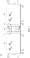
- FIG. 1 is a schematic view of an integrated circuit device according to an embodiment of the disclosure. Please refer to FIG. 1 .
- the integrated circuit device 100 includes a reference voltage channel 110, a first cell 120 and a second cell 130.
- the reference voltage channel 110 is configured to provide a first reference voltage VDD and a second reference voltage VSS.
- the first reference voltage VDD is, for example, a system voltage
- the second reference voltage VSS is, for example, a ground voltage, but the disclosure is not limited thereto.
- the first cell 120 is coupled to the reference voltage channel 110, and is configured to receive the first reference voltage VDD and the second reference voltage VSS. In addition, the first cell 120 is disposed on a first side 111 of the reference voltage channel 110.
- the second cell 130 is coupled to the reference voltage channel 110, and is configured to receive the first reference voltage VDD and the second reference voltage VSS.
- the second cell 130 is disposed on a second side 112 of the reference voltage channel 110.
- the second side 112 is opposite to the first side 111. That is, the first cell 120 and the second cell 130 are disposed at two opposite sides of the reference voltage channel 110. Therefore, the first cell 120 and the second cell 130 may share the same reference voltage channel 110, the first cell 120 and the second cell 130 may share the same first reference voltage VDD and the same second reference voltage VSS, so as to effectively decrease the area and power consumption of the integrated circuit device 100.
- each of the first cell 120 and the second cell 130 may include a plurality of transistors.
- the transistors may at least include an N-type transistor TN and a P-type transistor TP, but the disclosure is not limited thereto.
- the transistors may also a plurality of N-type transistors TN and a plurality of P-type transistors TP.
- the number of transistors of the first cell 120 is, for example, equal to the number of transistors of the second cell 130. That is, the area of the first cell 120 is equal to the area the second cell 130.
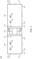
- the number of transistors of the first cell 120 is, for example, less than the number of transistors of the second cell 130, as shown in FIG. 2 . That is, the area of the first cell 120 is less than the area of the second cell 130.
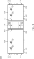
- the number of transistors of the first cell 120 is, for example, greater than the number of transistors of the second cell 130, as shown in FIG. 3 . That is, the area of the first cell 120 is greater than the area of the second cell 130.
- the first cell 120 may at least include an input terminal 121 and an output terminal 122.
- the input terminal 121 is configured to receive an input signal.
- the output terminal 122 is configured to output an output signal.
- the first cell 120 may include a plurality of input terminals 121 and a plurality of output terminals 122.
- the number of input terminals 121 and the number of output terminals 122 may be the same or different.
- the second cell 130 may at least include an input terminal 131 and an output terminal 132.
- the input terminal 131 is configured to receive an input signal.
- the output terminal 132 is configured to output an output signal.
- the second cell 130 may include a plurality of input terminals 131 and a plurality of output terminals 132.
- the number of input terminals 131 and the number of output terminals 132 may be the same or different.
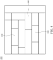
- FIG. 4 is a schematic view of a layout of a chip device according to an embodiment of the disclosure.
- the chip device 400 may include at least one integrated circuit device 100 in FIG. 1 , FIG. 2 and/or FIG. 3 . Therefore, the chip device 400 may also achieve the same effect for decreasing area and power consumption.
- the chip device 400 includes three integrated circuits 100, but the disclosure is not limited thereto.
- the chip device 400 may also include two or more than three integrated circuits 100.
- the disposing position of the integrated circuits 100 in FIG. 4 is one exemplary embodiment of the disclosure, but the disclosure is not limited thereto. The user may adjust the disposing position of the integrated circuits 100 according to the requirements thereof. Therefore, the same effect may also be achieved.
- FIG. 5 is a schematic view of an integrated circuit device according to an embodiment of the disclosure. Please refer to FIG. 5 .
- the integrated circuit device 500 includes a plurality of selecting modules 510_1 ⁇ 510_N and a selecting signal providing module 520, wherein N is a positive integer greater than 1.
- Each of the selecting modules 510_1 ⁇ 510_N is configured to receive a first input signal IN1_1 ⁇ IN1_N, a second input signal IN2_1 ⁇ IN2_N, a first selecting signal S1 and a second selecting signal S2, and select the first input signal IN1_1 ⁇ IN1_N or the second input signal IN2_1 ⁇ IN2_N to generate an output signal OUT_1 ⁇ OUT_N according to a first selecting signal S1 and a second selecting signal S2.
- the selecting modules 510_1 receives the first input signal IN1_1, the second input signal IN2_1, the first selecting signal S1 and the second selecting signal S2, and selects the first input signal IN1_1 or the second input signal IN2_1 to generate the output signal OUT_1 according to the first selecting signal S1 and the second selecting signal S2.
- the selecting modules 510_2 receives the first input signal IN1_2, the second input signal IN2_2, the first selecting signal S1 and the second selecting signal S2, and selects the first input signal IN1_2 or the second input signal IN2_2 to generate the output signal OUT_2 according to the first selecting signal S1 and the second selecting signal S2.
- the selecting modules 510_N receives the first input signal IN1_N, the second input signal IN2_N, the first selecting signal S1 and the second selecting signal S2, and selects the first input signal IN1_N or the second input signal IN2_N to generate the output signal OUT_N according to the first selecting signal S1 and the second selecting signal S2.
- each of the selecting modules 510_1 ⁇ 510_N may include, for example, a multiplexer (MUX).
- the selecting signal providing module 520 is coupled to the selecting module 510_1 ⁇ 510_N.
- the selecting signal providing module 520 is configured to provide the first selecting signal S1 and the second selecting signal S2.
- the selecting signal providing module 520 may include an inverter 521.
- the inverter 521 has an input terminal and an output terminal. The input terminal of the inverter 521 receives the first selecting signal S1, and the output terminal of the inverter 521 outputs the second selecting signal S2. Therefore, the selecting modules 510_1 ⁇ 510_N may share the same selecting signal providing module 520, i.e., the selecting modules 510_1 ⁇ 510_N may share the same first selecting signal S1 and the same second selecting signal S2, so as to decrease the area and power consumption of the integrated circuit device 500.
- the selecting module 510_1 may include a first transistor T1, a second transistor T2, a third transistor T3, a fourth transistor T4, a fifth transistor T5, a sixth transistor T6, a seventh transistor T7, an eighth transistor T8, a ninth transistor T9 and a tenth transistor T10, as shown in FIG. 6 .
- the internal components and the connection relationship thereof of selecting modules 510_2 ⁇ 510_N are the same as the internal components and the connection relationship thereof of the selecting module 510_1. Accordingly, the selecting modules 510_2 ⁇ 510_N may refer to the description of the embodiment in FIG. 6 , and the description thereof is not repeated thereto.
- the first transistor T1 has a first terminal, a second terminal and a control terminal.
- the first terminal of the first transistor T1 receives a first reference voltage VDD.
- the control terminal of the first transistor T1 receives the first input signal IN1_1.
- the second transistor T2 has a first terminal, a second terminal and a control terminal.
- the first terminal of the second transistor T2 receives a second reference voltage VSS.
- the second terminal of the second transistor T2 is coupled to the second terminal of the first transistor T1.
- the control terminal of the second transistor T2 is coupled to the control terminal of the first transistor T1.
- the first reference voltage VDD is, for example, a system voltage
- the second reference voltage VSS is, for example, a ground voltage.
- the third transistor T3 has a first terminal, a second terminal and a control terminal.
- the first terminal of the third transistor T3 receives the first reference voltage VDD.
- the control terminal of the third transistor T3 receives the second input signal IN2_1.
- the fourth transistor T4 has a first terminal, a second terminal and a control terminal.
- the first terminal of the fourth transistor T4 receives the second reference voltage VSS.
- the second terminal of the fourth transistor T4 is coupled to the second terminal of the third transistor T3.
- the control terminal of the fourth transistor T4 is coupled to the control terminal of the third transistor T3.
- the fifth transistor T5 has a first terminal, a second terminal and a control terminal.
- the first terminal of the fifth transistor T5 is coupled to the second terminal of the first transistor T1.
- the control terminal of the fifth transistor T5 receives the first selecting signal S1.
- the sixth transistor T6 has a first terminal, a second terminal and a control terminal.
- the first terminal of the sixth transistor T6 is coupled to the second terminal of the fifth transistor T5.
- the second terminal of the sixth transistor T6 is coupled to the first terminal of the fifth transistor T5.
- the control terminal of the sixth transistor T6 receives the second selecting signal S2.
- the seventh transistor T7 has a first terminal, a second terminal and a control terminal.
- the first terminal of the seventh transistor T7 is coupled to the second terminal of the third transistor T3.
- the control terminal of the seventh transistor T7 receives the second reference voltage S2.
- the eighth transistor T8 has a first terminal, a second terminal and a control terminal.
- the first terminal of the eighth transistor T8 is coupled to the second terminal of the seventh transistor T7.
- the second terminal of the eighth transistor T8 is coupled to the first terminal of the seventh transistor T7.
- the control terminal of the eighth transistor T8 receives the first selecting signal S1.
- the ninth transistor T9 has a first terminal, a second terminal and a control terminal.
- the first terminal of the ninth transistor T9 receives the first reference voltage VDD.
- the second terminal of the ninth transistor T9 generates the first output signal OUT_1.
- the control terminal of the ninth transistor T9 is coupled to the second terminal of the fifth transistor T5 and the second terminal of the seventh transistor T7.
- the tenth transistor T10 has a first terminal, a second terminal and a control terminal.
- the first terminal of the tenth transistor T10 receives the second reference voltage VSS.
- the second terminal of the tenth transistor T10 is coupled to the second terminal of the ninth transistor T9.
- the control terminal of the tenth transistor T10 is coupled to the control terminal of the ninth transistor T9.
- each of the first transistor T1, the third transistor T3, the fifth transistor T5, the seventh transistor T7 and the ninth transistor T9 is, for example, a P-type transistor.
- Each of the first terminals of the first transistor T1, the third transistor T3, the fifth transistor T5, the seventh transistor T7 and the ninth transistor T9 is, for example, a source terminal of the P-type transistor.
- Each of the second terminals of the first transistor T1, the third transistor T3, the fifth transistor T5, the seventh transistor T7 and the ninth transistor T9 is, for example, a drain terminal of the P-type transistor.
- Each of the control terminals of the first transistor T1, the third transistor T3, the fifth transistor T5, the seventh transistor T7 and the ninth transistor T9 is, for example, a gate terminal of the P-type transistor.
- each of the second transistor T2, the fourth transistor T4, the sixth transistor T6, the eighth transistor T8 and the tenth transistor T10 is, for example, an N-type transistor.
- Each of the first terminals of the second transistor T2, the fourth transistor T4, the sixth transistor T6, the eighth transistor T8 and the tenth transistor T10 is, for example, a source terminal of the N-type transistor.
- Each of the second terminals of the second transistor T2, the fourth transistor T4, the sixth transistor T6, the eighth transistor T8 and the tenth transistor T10 is, for example, a drain terminal of the N-type transistor.
- Each of the control terminals of the second transistor T2, the fourth transistor T4, the sixth transistor T6, the eighth transistor T8 and the tenth transistor T10 is, for example, a gate terminal of the P-type transistor.
- the selecting module 510_1 may include a first transistor T11, a second transistor T12, a third transistor T13, a fourth transistor T14, a fifth transistor T15, a sixth transistor T16, a seventh transistor T17, an eighth transistor T18, a ninth transistor T19 and a tenth transistor T20, as shown in FIG. 7 .
- the internal components and the connection relationship thereof of selecting modules 510_2 ⁇ 510_N are the same as the internal components and the connection relationship thereof of the selecting module 510_1. Accordingly, the selecting modules 510_2 ⁇ 510_N may refer to the description of the embodiment in FIG. 6 , and the description thereof is not repeated thereto.
- the first transistor T11 has a first terminal, a second terminal and a control terminal.
- the first terminal of the first transistor T11 receives a first reference voltage VDD.
- the control terminal of the first transistor T11 receives the second selecting signal S2.
- the second transistor T12 has a first terminal, a second terminal and a control terminal.
- the first terminal of the second transistor T12 receives the first reference voltage VDD.
- the second terminal of the second transistor T12 is coupled to the second terminal of the first transistor T11.
- the control terminal of the second transistor T12 receives the first input signal IN1_1.
- the third transistor T13 has a first terminal, a second terminal and a control terminal.
- the first terminal of the third transistor T13 is coupled to the second terminal of the first transistor T11.
- the control terminal of the third transistor T13 receives the first selecting signal S1.
- the fourth transistor T14 has a first terminal, a second terminal and a control terminal.
- the first terminal of the fourth transistor T14 is coupled to the first terminal of the third transistor T13.
- the second terminal of the fourth transistor T14 is coupled to the second terminal of the third transistor T13.
- the control terminal of the fourth transistor T14 receives the second input signal IN2_1.
- the fifth transistor T15 has a first terminal, a second terminal and a control terminal.
- the second terminal of the fifth transistor T15 is coupled to the second terminal of the third transistor T13.
- the control terminal of the fifth transistor T15 receives the first selecting signal S1.
- the sixth transistor T16 has a first terminal, a second terminal and a control terminal.
- the second terminal of the sixth transistor T16 is coupled to the second terminal of fifth transistor T15.
- the control terminal of the sixth transistor T16 receives the second selecting signal S2.
- the seventh transistor T17 has a first terminal, a second terminal and a control terminal.
- the first terminal of the seventh transistor T17 receives the second reference voltage VSS.
- the second terminal of the seventh transistor T17 is coupled to the first terminal of the fifth transistor T15.
- the control terminal of the seventh transistor T17 receives the first input signal IN1_1.
- the eighth transistor T18 has a first terminal, a second terminal and a control terminal.
- the first terminal of the eighth transistor T18 receives the second reference voltage VSS.
- the second terminal of the eighth transistor T18 is coupled to the first terminal of the sixth transistor T16.
- the control terminal of the eighth transistor T18 receives the second input signal IN2_1.
- the ninth transistor T19 has a first terminal, a second terminal and a control terminal.
- the first terminal of the ninth transistor T19 receives the first reference voltage VDD.
- the second terminal of the ninth transistor T19 generates the first output signal OUT_1.
- the control terminal of the ninth transistor T19 is coupled to the second terminal of the third transistor T13.
- the tenth transistor T20 has a first terminal, a second terminal and a control terminal.
- the first terminal of the tenth transistor T20 receives the second reference voltage VSS.
- the second terminal of the tenth transistor T20 is coupled to the second terminal of the ninth transistor T19.
- the control terminal of the tenth transistor T20 is coupled to the control terminal of the ninth transistor T19.
- each of the first transistor T11, the second transistor T12, the third transistor T13, the fourth transistor T14 and the ninth transistor T19 is, for example, a P-type transistor.
- Each of the first terminals of the first transistor T11, the second transistor T12, the third transistor T13, the fourth transistor T14 and the ninth transistor T19 is, for example, a source terminal of the P-type transistor.
- Each of the second terminals of the first transistor T11, the second transistor T12, the third transistor T13, the fourth transistor T14 and the ninth transistor T19 is, for example, a drain terminal of the P-type transistor.
- Each of the control terminals of the first transistor T11, the second transistor T12, the third transistor T13, the fourth transistor T14 and the ninth transistor T19 is, for example, a gate terminal of the P-type transistor.
- each of the fifth transistor T15, the sixth transistor T16, the seventh transistor T17, the eighth transistor T18 and the tenth transistor T20 is, for example, an N-type transistor.
- Each of the first terminals the fifth transistor T15, the sixth transistor T16, the seventh transistor T17, the eighth transistor T18 and the tenth transistor T20 is, for example, a source terminal of the N-type transistor.
- Each of the second terminals of the fifth transistor T15, the sixth transistor T16, the seventh transistor T17, the eighth transistor T18 and the tenth transistor T20 is, for example, a drain terminal of the N-type transistor.
- Each of the control terminals of the fifth transistor T15, the sixth transistor T16, the seventh transistor T17, the eighth transistor T18 and the tenth transistor T20 is, for example, a gate terminal of the P-type transistor.
- the first cell and the second cell share the same reference voltage channel (i.e., the same first reference voltage and the same second reference voltage) or the selecting modules share the same selecting signal providing module (i.e., the same first selecting signal and the same second selecting signal). Therefore, the area and power consumption of the integrated circuit device may be effectively decreased.
Landscapes
- Engineering & Computer Science (AREA)
- Computer Hardware Design (AREA)
- Physics & Mathematics (AREA)
- Computing Systems (AREA)
- General Engineering & Computer Science (AREA)
- Mathematical Physics (AREA)
- Semiconductor Integrated Circuits (AREA)
- Control Of Electrical Variables (AREA)
Abstract
Description
- The disclosure relates to an integrated circuit, and, in particular, to an integrated circuit device and a chip device for decreasing area and power consumption.
- Generally, an integrated circuit may include a plurality of components. However, each of the components may use an independent power source, or the selecting signal of an independent selecting module, increasing the area and power consumption of the integrated circuit. Therefore, how to decrease the area and power consumption of the integrated circuit has become an important issue.
- The disclosure provides an integrated circuit device and a chip device, thereby decreasing the area and power consumption of the integrated circuit device.
- According to a first aspect of the invention, an integrated circuit device includes a reference voltage channel, a first cell and a second cell. The reference voltage channel is configured to provide a first reference voltage and a second reference voltage. The first cell is coupled to the reference voltage channel, and is configured to receive the first reference voltage and the second reference voltage. The second cell is coupled to the reference voltage channel, and is configured to receive the first reference voltage and the second reference voltage.
- An embodiment of the disclosure provides a chip device, which includes at least one above integrated circuit device.
- An embodiment of the disclosure provides an integrated circuit device, which includes a plurality of selecting modules and a selecting signal providing module. Each of the selecting modules is configured to receive a first input signal, a second input signal, a first selecting signal and a second selecting signal, and select the first input signal or the second input signal to generate an output signal according to a first selecting signal and a second selecting signal. The selecting signal providing module is configured to provide the first selecting signal and the second selecting signal.
- According to a second aspect of the invention, an integrated circuit device, comprises: a plurality of selecting modules, wherein each of the plurality of selecting modules is configured to receive a first input signal, a second input signal, a first selecting signal and a second selecting signal, and select the first input signal or the second input signal to generate an output signal according to a first selecting signal and a second selecting signal; and a selecting signal providing module, configured to provide the first selecting signal and the second selecting signal.
- Preferably, the first selecting signal and the second selecting signal are inverted.
- The module advantageously comprises: an inverter, having an input terminal and an output terminal, wherein the input terminal of the inverter receives the first selecting signal, and the output terminal of the inverter outputs the second selecting signal.
- Each of the plurality of selecting modules may comprise a multiplexer.
- Each of the plurality of selecting modules advantageously comprises: a first transistor, having a first terminal, a second terminal and a control terminal, wherein the first terminal of the first transistor receives a first reference voltage, and the control terminal of the first transistor receives the first input signal; a second transistor, having a first terminal, a second terminal and a control terminal, wherein the first terminal of the second transistor receives a second reference voltage, the second terminal of the second transistor is coupled to the second terminal of the first transistor, and the control terminal of the second transistor is coupled to the control terminal of the first transistor; a third transistor, having a first terminal, a second terminal and a control terminal, wherein the first terminal of the third transistor receives the first reference voltage, and the control terminal of the third transistor receives the second input signal; a fourth transistor, having a first terminal, a second terminal and a control terminal, wherein the first terminal of the fourth transistor receives the second reference voltage, the second terminal of the fourth transistor is coupled to the second terminal of the third transistor, and the control terminal of the fourth transistor is coupled to the control terminal of the third transistor; a fifth transistor, having a first terminal, a second terminal and a control terminal, wherein the first terminal of the fifth transistor is coupled to the second terminal of the first transistor, and the control terminal of the fifth transistor receives the first selecting signal; a sixth transistor, having a first terminal, a second terminal and a control terminal, wherein the first terminal of the sixth transistor is coupled to the second terminal of the fifth transistor, the second terminal of the sixth transistor is coupled to the first terminal of the fifth transistor, and the control terminal of the sixth transistor receives the second selecting signal; a seventh transistor, having a first terminal, a second terminal and a control terminal, wherein the first terminal of the seventh transistor is coupled to the second terminal of the third transistor, and the control terminal of the seventh transistor receives the second reference voltage; an eighth transistor, having a first terminal, a second terminal and a control terminal, wherein the first terminal of the eighth transistor is coupled to the second terminal of the seventh transistor, the second terminal of the eighth transistor is coupled to the first terminal of the seventh transistor, and the control terminal of the eighth transistor receives the first selecting signal; a ninth transistor, having a first terminal, a second terminal and a control terminal, wherein the first terminal of the ninth transistor receives the first reference voltage, and the second terminal of the ninth transistor generates the first output signal, and the control terminal of the ninth transistor is coupled to the second terminal of the fifth transistor and the second terminal of the seventh transistor; a tenth transistor, having a first terminal, a second terminal and a control terminal, wherein the first terminal of the tenth transistor receives the second reference voltage, the second terminal of the tenth transistor is coupled to the second terminal of the ninth transistor, and the control terminal of the tenth transistor is coupled to the control terminal of the ninth transistor.
- Each of the first transistor, the third transistor, the fifth transistor, the seventh transistor and the ninth transistor is a P-type transistor, and each of the second transistor, the fourth transistor, the sixth transistor, the eighth transistor and the tenth transistor is an N-type transistor.
- Each of the plurality of selecting modules may comprise: a first transistor, having a first terminal, a second terminal and a control terminal, wherein the first terminal of the first transistor receives a first reference voltage, and the control terminal of the first transistor receives the second selecting signal; a second transistor, having a first terminal, a second terminal and a control terminal, wherein the first terminal of the second transistor receives the first reference voltage, the second terminal of the second transistor is coupled to the second terminal of the first transistor, and the control terminal of the second transistor receives the first input signal; a third transistor, having a first terminal, a second terminal and a control terminal, wherein the first terminal of the third transistor is coupled to the second terminal of the first transistor, and the control terminal of the third transistor receives the first selecting signal; a fourth transistor, having a first terminal, a second terminal and a control terminal, wherein the first terminal of the fourth transistor is coupled to the first terminal of the third transistor, the second terminal of the fourth transistor is coupled to the second terminal of the third transistor, and the control terminal of the fourth transistor receives the second input signal; a fifth transistor, having a first terminal, a second terminal and a control terminal, wherein the second terminal of the fifth transistor is coupled to the second terminal of the third transistor, and the control terminal of the fifth transistor receives the first selecting signal; a sixth transistor, having a first terminal, a second terminal and a control terminal, wherein the second terminal of the sixth transistor is coupled to the second terminal of fifth transistor, and the control terminal of the sixth transistor receives the second selecting signal; a seventh transistor, having a first terminal, a second terminal and a control terminal, wherein the first terminal of the seventh transistor receives the second reference voltage, the second terminal of the seventh transistor is coupled to the first terminal of the fifth transistor, and the control terminal of the seventh transistor receives the first input signal; an eighth transistor, having a first terminal, a second terminal and a control terminal, wherein the first terminal of the eighth transistor receives the second reference voltage, the second terminal of the eighth transistor is coupled to the first terminal of the sixth transistor, and the control terminal of the eighth transistor receives the second input signal; a ninth transistor, having a first terminal, a second terminal and a control terminal, wherein the first terminal of the ninth transistor receives the first reference voltage, the second terminal of the ninth transistor generates the first output signal, and the control terminal of the ninth transistor is coupled to the second terminal of the third transistor; and a tenth transistor, having a first terminal, a second terminal and a control terminal, wherein the first terminal of the tenth transistor receives the second reference voltage, the second terminal of the tenth transistor is coupled to the second terminal of the ninth transistor, and the control terminal of the tenth transistor is coupled to the control terminal of the ninth transistor.
- Each of the first transistor, the second transistor, the third transistor, the fourth transistor and the ninth transistor may be a P-type transistor, and each of the fifth transistor, the sixth transistor, the seventh transistor, the eighth transistor and the tenth transistor may be an N-type transistor.
- The disclosure can be more fully understood by reading the subsequent detailed description and examples with references made to the accompanying drawings, wherein:
-
FIG. 1 is a schematic view of an integrated circuit device according to an embodiment of the disclosure; -
FIG. 2 is a schematic view of an integrated circuit device according to another embodiment of the disclosure; -
FIG. 3 is a schematic view of an integrated circuit device according to another embodiment of the disclosure; -
FIG. 4 is a schematic view of a layout of a chip device according to an embodiment of the disclosure; -
FIG. 5 is a schematic view of an integrated circuit device according to an embodiment of the disclosure; -
FIG. 6 is a circuit diagram of a selecting module inFIG. 5 ; and -
FIG. 7 is a circuit diagram of a selecting module inFIG. 5 . - Technical terms of the present disclosure are based on general definition in the technical field of the present disclosure. If the present disclosure describes or explains one or some terms, definition of the terms is based on the description or explanation of the present disclosure. Each of the disclosed embodiments has one or more technical features. In possible implementation, a person skilled in the art would selectively implement all or some technical features of any embodiment of the present disclosure or selectively combine all or some technical features of the embodiments of the present disclosure.
- In each of the following embodiments, the same reference number represents the same or a similar element or component.
-
FIG. 1 is a schematic view of an integrated circuit device according to an embodiment of the disclosure. Please refer toFIG. 1 . Theintegrated circuit device 100 includes areference voltage channel 110, afirst cell 120 and asecond cell 130. - The
reference voltage channel 110 is configured to provide a first reference voltage VDD and a second reference voltage VSS. In the embodiment, the first reference voltage VDD is, for example, a system voltage, and the second reference voltage VSS is, for example, a ground voltage, but the disclosure is not limited thereto. - The
first cell 120 is coupled to thereference voltage channel 110, and is configured to receive the first reference voltage VDD and the second reference voltage VSS. In addition, thefirst cell 120 is disposed on afirst side 111 of thereference voltage channel 110. - The
second cell 130 is coupled to thereference voltage channel 110, and is configured to receive the first reference voltage VDD and the second reference voltage VSS. In addition, thesecond cell 130 is disposed on asecond side 112 of thereference voltage channel 110. Thesecond side 112 is opposite to thefirst side 111. That is, thefirst cell 120 and thesecond cell 130 are disposed at two opposite sides of thereference voltage channel 110. Therefore, thefirst cell 120 and thesecond cell 130 may share the samereference voltage channel 110, thefirst cell 120 and thesecond cell 130 may share the same first reference voltage VDD and the same second reference voltage VSS, so as to effectively decrease the area and power consumption of theintegrated circuit device 100. - In some embodiments, each of the
first cell 120 and thesecond cell 130 may include a plurality of transistors. In addition, the transistors may at least include an N-type transistor TN and a P-type transistor TP, but the disclosure is not limited thereto. In other embodiments, the transistors may also a plurality of N-type transistors TN and a plurality of P-type transistors TP. - In the embodiment, the number of transistors of the
first cell 120 is, for example, equal to the number of transistors of thesecond cell 130. That is, the area of thefirst cell 120 is equal to the area thesecond cell 130. - In some embodiments, the number of transistors of the
first cell 120 is, for example, less than the number of transistors of thesecond cell 130, as shown inFIG. 2 . That is, the area of thefirst cell 120 is less than the area of thesecond cell 130. - In some embodiments, the number of transistors of the
first cell 120 is, for example, greater than the number of transistors of thesecond cell 130, as shown inFIG. 3 . That is, the area of thefirst cell 120 is greater than the area of thesecond cell 130. - In some embodiments, the
first cell 120 may at least include aninput terminal 121 and anoutput terminal 122. Theinput terminal 121 is configured to receive an input signal. Theoutput terminal 122 is configured to output an output signal. In other embodiments, thefirst cell 120 may include a plurality ofinput terminals 121 and a plurality ofoutput terminals 122. In addition, the number ofinput terminals 121 and the number ofoutput terminals 122 may be the same or different. - In addition, the
second cell 130 may at least include aninput terminal 131 and anoutput terminal 132. Theinput terminal 131 is configured to receive an input signal. Theoutput terminal 132 is configured to output an output signal. In other embodiments, thesecond cell 130 may include a plurality ofinput terminals 131 and a plurality ofoutput terminals 132. In addition, the number ofinput terminals 131 and the number ofoutput terminals 132 may be the same or different. -
FIG. 4 is a schematic view of a layout of a chip device according to an embodiment of the disclosure. Please refer toFIG. 4 . Thechip device 400 may include at least oneintegrated circuit device 100 inFIG. 1 ,FIG. 2 and/orFIG. 3 . Therefore, thechip device 400 may also achieve the same effect for decreasing area and power consumption. InFIG. 4 , thechip device 400 includes threeintegrated circuits 100, but the disclosure is not limited thereto. In some embodiment, thechip device 400 may also include two or more than threeintegrated circuits 100. In addition, the disposing position of theintegrated circuits 100 inFIG. 4 is one exemplary embodiment of the disclosure, but the disclosure is not limited thereto. The user may adjust the disposing position of theintegrated circuits 100 according to the requirements thereof. Therefore, the same effect may also be achieved. -
FIG. 5 is a schematic view of an integrated circuit device according to an embodiment of the disclosure. Please refer toFIG. 5 . Theintegrated circuit device 500 includes a plurality of selecting modules 510_1~510_N and a selectingsignal providing module 520, wherein N is a positive integer greater than 1. - Each of the selecting modules 510_1~510_N is configured to receive a first input signal IN1_1~IN1_N, a second input signal IN2_1~IN2_N, a first selecting signal S1 and a second selecting signal S2, and select the first input signal IN1_1~IN1_N or the second input signal IN2_1~IN2_N to generate an output signal OUT_1~OUT_N according to a first selecting signal S1 and a second selecting signal S2. For example, the selecting modules 510_1 receives the first input signal IN1_1, the second input signal IN2_1, the first selecting signal S1 and the second selecting signal S2, and selects the first input signal IN1_1 or the second input signal IN2_1 to generate the output signal OUT_1 according to the first selecting signal S1 and the second selecting signal S2.
- The selecting modules 510_2 receives the first input signal IN1_2, the second input signal IN2_2, the first selecting signal S1 and the second selecting signal S2, and selects the first input signal IN1_2 or the second input signal IN2_2 to generate the output signal OUT_2 according to the first selecting signal S1 and the second selecting signal S2.... The selecting modules 510_N receives the first input signal IN1_N, the second input signal IN2_N, the first selecting signal S1 and the second selecting signal S2, and selects the first input signal IN1_N or the second input signal IN2_N to generate the output signal OUT_N according to the first selecting signal S1 and the second selecting signal S2. In the embodiments, each of the selecting modules 510_1~510_N may include, for example, a multiplexer (MUX).
- The selecting
signal providing module 520 is coupled to the selecting module 510_1~510_N. The selectingsignal providing module 520 is configured to provide the first selecting signal S1 and the second selecting signal S2. - In the embodiment, the first selecting signal S1 and the second selecting signal S2 are inverted. In addition, the selecting
signal providing module 520 may include aninverter 521. Theinverter 521 has an input terminal and an output terminal. The input terminal of theinverter 521 receives the first selecting signal S1, and the output terminal of theinverter 521 outputs the second selecting signal S2. Therefore, the selecting modules 510_1~510_N may share the same selectingsignal providing module 520, i.e., the selecting modules 510_1~510_N may share the same first selecting signal S1 and the same second selecting signal S2, so as to decrease the area and power consumption of theintegrated circuit device 500. - In some embodiments, the selecting module 510_1 may include a first transistor T1, a second transistor T2, a third transistor T3, a fourth transistor T4, a fifth transistor T5, a sixth transistor T6, a seventh transistor T7, an eighth transistor T8, a ninth transistor T9 and a tenth transistor T10, as shown in
FIG. 6 . The internal components and the connection relationship thereof of selecting modules 510_2~510_N are the same as the internal components and the connection relationship thereof of the selecting module 510_1. Accordingly, the selecting modules 510_2~510_N may refer to the description of the embodiment inFIG. 6 , and the description thereof is not repeated thereto. - The first transistor T1 has a first terminal, a second terminal and a control terminal. The first terminal of the first transistor T1 receives a first reference voltage VDD. The control terminal of the first transistor T1 receives the first input signal IN1_1. The second transistor T2 has a first terminal, a second terminal and a control terminal. The first terminal of the second transistor T2 receives a second reference voltage VSS. The second terminal of the second transistor T2 is coupled to the second terminal of the first transistor T1. The control terminal of the second transistor T2 is coupled to the control terminal of the first transistor T1. In the embodiments, the first reference voltage VDD is, for example, a system voltage, and the second reference voltage VSS is, for example, a ground voltage.
- The third transistor T3 has a first terminal, a second terminal and a control terminal. The first terminal of the third transistor T3 receives the first reference voltage VDD. The control terminal of the third transistor T3 receives the second input signal IN2_1. The fourth transistor T4 has a first terminal, a second terminal and a control terminal. The first terminal of the fourth transistor T4 receives the second reference voltage VSS. The second terminal of the fourth transistor T4 is coupled to the second terminal of the third transistor T3. The control terminal of the fourth transistor T4 is coupled to the control terminal of the third transistor T3.
- The fifth transistor T5 has a first terminal, a second terminal and a control terminal. The first terminal of the fifth transistor T5 is coupled to the second terminal of the first transistor T1. The control terminal of the fifth transistor T5 receives the first selecting signal S1. The sixth transistor T6 has a first terminal, a second terminal and a control terminal. The first terminal of the sixth transistor T6 is coupled to the second terminal of the fifth transistor T5. The second terminal of the sixth transistor T6 is coupled to the first terminal of the fifth transistor T5. The control terminal of the sixth transistor T6 receives the second selecting signal S2.
- The seventh transistor T7 has a first terminal, a second terminal and a control terminal. The first terminal of the seventh transistor T7 is coupled to the second terminal of the third transistor T3. The control terminal of the seventh transistor T7 receives the second reference voltage S2. The eighth transistor T8 has a first terminal, a second terminal and a control terminal. The first terminal of the eighth transistor T8 is coupled to the second terminal of the seventh transistor T7. The second terminal of the eighth transistor T8 is coupled to the first terminal of the seventh transistor T7. The control terminal of the eighth transistor T8 receives the first selecting signal S1.
- The ninth transistor T9 has a first terminal, a second terminal and a control terminal. The first terminal of the ninth transistor T9 receives the first reference voltage VDD. The second terminal of the ninth transistor T9 generates the first output signal OUT_1. The control terminal of the ninth transistor T9 is coupled to the second terminal of the fifth transistor T5 and the second terminal of the seventh transistor T7. The tenth transistor T10 has a first terminal, a second terminal and a control terminal. The first terminal of the tenth transistor T10 receives the second reference voltage VSS. The second terminal of the tenth transistor T10 is coupled to the second terminal of the ninth transistor T9. The control terminal of the tenth transistor T10 is coupled to the control terminal of the ninth transistor T9.
- In some embodiments, each of the first transistor T1, the third transistor T3, the fifth transistor T5, the seventh transistor T7 and the ninth transistor T9 is, for example, a P-type transistor. Each of the first terminals of the first transistor T1, the third transistor T3, the fifth transistor T5, the seventh transistor T7 and the ninth transistor T9 is, for example, a source terminal of the P-type transistor. Each of the second terminals of the first transistor T1, the third transistor T3, the fifth transistor T5, the seventh transistor T7 and the ninth transistor T9 is, for example, a drain terminal of the P-type transistor. Each of the control terminals of the first transistor T1, the third transistor T3, the fifth transistor T5, the seventh transistor T7 and the ninth transistor T9 is, for example, a gate terminal of the P-type transistor.
- In addition, each of the second transistor T2, the fourth transistor T4, the sixth transistor T6, the eighth transistor T8 and the tenth transistor T10 is, for example, an N-type transistor. Each of the first terminals of the second transistor T2, the fourth transistor T4, the sixth transistor T6, the eighth transistor T8 and the tenth transistor T10 is, for example, a source terminal of the N-type transistor. Each of the second terminals of the second transistor T2, the fourth transistor T4, the sixth transistor T6, the eighth transistor T8 and the tenth transistor T10 is, for example, a drain terminal of the N-type transistor. Each of the control terminals of the second transistor T2, the fourth transistor T4, the sixth transistor T6, the eighth transistor T8 and the tenth transistor T10 is, for example, a gate terminal of the P-type transistor.
- In some embodiments, the selecting module 510_1 may include a first transistor T11, a second transistor T12, a third transistor T13, a fourth transistor T14, a fifth transistor T15, a sixth transistor T16, a seventh transistor T17, an eighth transistor T18, a ninth transistor T19 and a tenth transistor T20, as shown in
FIG. 7 . The internal components and the connection relationship thereof of selecting modules 510_2~510_N are the same as the internal components and the connection relationship thereof of the selecting module 510_1. Accordingly, the selecting modules 510_2~510_N may refer to the description of the embodiment inFIG. 6 , and the description thereof is not repeated thereto. - The first transistor T11 has a first terminal, a second terminal and a control terminal. The first terminal of the first transistor T11 receives a first reference voltage VDD. The control terminal of the first transistor T11 receives the second selecting signal S2. The second transistor T12 has a first terminal, a second terminal and a control terminal. The first terminal of the second transistor T12 receives the first reference voltage VDD. The second terminal of the second transistor T12 is coupled to the second terminal of the first transistor T11. The control terminal of the second transistor T12 receives the first input signal IN1_1.
- The third transistor T13 has a first terminal, a second terminal and a control terminal. The first terminal of the third transistor T13 is coupled to the second terminal of the first transistor T11. The control terminal of the third transistor T13 receives the first selecting signal S1. The fourth transistor T14 has a first terminal, a second terminal and a control terminal. The first terminal of the fourth transistor T14 is coupled to the first terminal of the third transistor T13. The second terminal of the fourth transistor T14 is coupled to the second terminal of the third transistor T13. The control terminal of the fourth transistor T14 receives the second input signal IN2_1.
- The fifth transistor T15 has a first terminal, a second terminal and a control terminal. The second terminal of the fifth transistor T15 is coupled to the second terminal of the third transistor T13. The control terminal of the fifth transistor T15 receives the first selecting signal S1. The sixth transistor T16 has a first terminal, a second terminal and a control terminal. The second terminal of the sixth transistor T16 is coupled to the second terminal of fifth transistor T15. The control terminal of the sixth transistor T16 receives the second selecting signal S2.
- The seventh transistor T17 has a first terminal, a second terminal and a control terminal. The first terminal of the seventh transistor T17 receives the second reference voltage VSS. The second terminal of the seventh transistor T17 is coupled to the first terminal of the fifth transistor T15. The control terminal of the seventh transistor T17 receives the first input signal IN1_1. The eighth transistor T18 has a first terminal, a second terminal and a control terminal. The first terminal of the eighth transistor T18 receives the second reference voltage VSS. The second terminal of the eighth transistor T18 is coupled to the first terminal of the sixth transistor T16. The control terminal of the eighth transistor T18 receives the second input signal IN2_1.
- The ninth transistor T19 has a first terminal, a second terminal and a control terminal. The first terminal of the ninth transistor T19 receives the first reference voltage VDD. The second terminal of the ninth transistor T19 generates the first output signal OUT_1. The control terminal of the ninth transistor T19 is coupled to the second terminal of the third transistor T13. The tenth transistor T20 has a first terminal, a second terminal and a control terminal. The first terminal of the tenth transistor T20 receives the second reference voltage VSS. The second terminal of the tenth transistor T20 is coupled to the second terminal of the ninth transistor T19. The control terminal of the tenth transistor T20 is coupled to the control terminal of the ninth transistor T19.
- In some embodiments, each of the first transistor T11, the second transistor T12, the third transistor T13, the fourth transistor T14 and the ninth transistor T19 is, for example, a P-type transistor. Each of the first terminals of the first transistor T11, the second transistor T12, the third transistor T13, the fourth transistor T14 and the ninth transistor T19 is, for example, a source terminal of the P-type transistor. Each of the second terminals of the first transistor T11, the second transistor T12, the third transistor T13, the fourth transistor T14 and the ninth transistor T19 is, for example, a drain terminal of the P-type transistor. Each of the control terminals of the first transistor T11, the second transistor T12, the third transistor T13, the fourth transistor T14 and the ninth transistor T19 is, for example, a gate terminal of the P-type transistor.
- In addition, each of the fifth transistor T15, the sixth transistor T16, the seventh transistor T17, the eighth transistor T18 and the tenth transistor T20 is, for example, an N-type transistor. Each of the first terminals the fifth transistor T15, the sixth transistor T16, the seventh transistor T17, the eighth transistor T18 and the tenth transistor T20 is, for example, a source terminal of the N-type transistor. Each of the second terminals of the fifth transistor T15, the sixth transistor T16, the seventh transistor T17, the eighth transistor T18 and the tenth transistor T20 is, for example, a drain terminal of the N-type transistor. Each of the control terminals of the fifth transistor T15, the sixth transistor T16, the seventh transistor T17, the eighth transistor T18 and the tenth transistor T20 is, for example, a gate terminal of the P-type transistor.
- In summary, according to the integrated circuit device and chip device disclosed by the present disclosure, the first cell and the second cell share the same reference voltage channel (i.e., the same first reference voltage and the same second reference voltage) or the selecting modules share the same selecting signal providing module (i.e., the same first selecting signal and the same second selecting signal). Therefore, the area and power consumption of the integrated circuit device may be effectively decreased.
- While the disclosure has been described by way of example and in terms of the preferred embodiments, it should be understood that the disclosure is not limited to the disclosed embodiments. On the contrary, it is intended to cover various modifications and similar arrangements (as would be apparent to those skilled in the art). Therefore, the scope of the appended claims should be accorded the broadest interpretation so as to encompass all such modifications and similar arrangements.
- List of Advantageous Features:
- 1. An integrated circuit device, comprising:
- a reference voltage channel, configured to provide a first reference voltage and a second reference voltage;
- a first cell, coupled to the reference voltage channel, and configured to receive the first reference voltage and the second reference voltage; and
- a second cell, coupled to the reference voltage channel, and configured to receive the first reference voltage and the second reference voltage.
- 2. The integrated circuit device of
feature 1, wherein the first reference voltage is a system voltage, and the second reference voltage is a ground voltage. - 3. The integrated circuit device oof
feature - 4. The integrated circuit device of
feature 3, wherein the plurality of transistors at least comprise an N-type transistor and a P-type transistor. - 5. The integrated circuit device of feature 4, wherein a number of the plurality of transistors of the first cell is equal to a number of the plurality of transistors of the second cell.
- 6. The integrated circuit device of
feature 3 or 4, wherein a number of the plurality of transistors of the first cell is less than a number of the plurality of transistors of the second cell. - 7. The integrated circuit device of
feature 3 or 4, wherein a number of the plurality of transistors of the first cell is greater than a number of the plurality of transistors of the second cell. - 8. The integrated circuit device of any of the preceding features, wherein the first cell comprises an input terminal and an output terminal.
- 9. The integrated circuit device of any one of the preceding features, wherein the second cell comprises an input terminal and an output terminal.
- 10. The integrated circuit device of any one of the preceding features, wherein the first cell is disposed on a first side of the reference voltage channel, and the second cell is disposed on a second side of the reference voltage channel.
- 11. The integrated circuit device of feature 10, wherein the second side is opposite to the first side.
- 12. A chip device, comprising at least one integrated circuit device of any one of
features 1 to 11.
Claims (9)
- An integrated circuit device, comprising:a plurality of selecting modules, wherein each of the plurality of selecting modules is configured to receive a first input signal, a second input signal, a first selecting signal and a second selecting signal, and select the first input signal or the second input signal to generate an output signal according to a first selecting signal and a second selecting signal; anda selecting signal providing module, configured to provide the first selecting signal and the second selecting signal.
- The integrated circuit device as claimed in claim 1, wherein the first selecting signal and the second selecting signal are inverted.
- The integrated circuit device as claimed in claim 1 or 2, wherein the selecting signal providing module comprises:
an inverter, having an input terminal and an output terminal, wherein the input terminal of the inverter receives the first selecting signal, and the output terminal of the inverter outputs the second selecting signal. - The integrated circuit device as claimed in any one of claims 1 to 3, wherein each of the plurality of selecting modules comprises a multiplexer.
- The integrated circuit device as claimed in any one of the preceding claims, wherein each of the plurality of selecting modules comprises:a first transistor, having a first terminal, a second terminal and a control terminal, wherein the first terminal of the first transistor receives a first reference voltage, and the control terminal of the first transistor receives the first input signal;a second transistor, having a first terminal, a second terminal and a control terminal, wherein the first terminal of the second transistor receives a second reference voltage, the second terminal of the second transistor is coupled to the second terminal of the first transistor, and the control terminal of the second transistor is coupled to the control terminal of the first transistor;a third transistor, having a first terminal, a second terminal and a control terminal, wherein the first terminal of the third transistor receives the first reference voltage, and the control terminal of the third transistor receives the second input signal;a fourth transistor, having a first terminal, a second terminal and a control terminal, wherein the first terminal of the fourth transistor receives the second reference voltage, the second terminal of the fourth transistor is coupled to the second terminal of the third transistor, and the control terminal of the fourth transistor is coupled to the control terminal of the third transistor;a fifth transistor, having a first terminal, a second terminal and a control terminal, wherein the first terminal of the fifth transistor is coupled to the second terminal of the first transistor, and the control terminal of the fifth transistor receives the first selecting signal;a sixth transistor, having a first terminal, a second terminal and a control terminal, wherein the first terminal of the sixth transistor is coupled to the second terminal of the fifth transistor, the second terminal of the sixth transistor is coupled to the first terminal of the fifth transistor, and the control terminal of the sixth transistor receives the second selecting signal;a seventh transistor, having a first terminal, a second terminal and a control terminal, wherein the first terminal of the seventh transistor is coupled to the second terminal of the third transistor, and the control terminal of the seventh transistor receives the second reference voltage;an eighth transistor, having a first terminal, a second terminal and a control terminal, wherein the first terminal of the eighth transistor is coupled to the second terminal of the seventh transistor, the second terminal of the eighth transistor is coupled to the first terminal of the seventh transistor, and the control terminal of the eighth transistor receives the first selecting signal;a ninth transistor, having a first terminal, a second terminal and a control terminal, wherein the first terminal of the ninth transistor receives the first reference voltage, and the second terminal of the ninth transistor generates the first output signal, and the control terminal of the ninth transistor is coupled to the second terminal of the fifth transistor and the second terminal of the seventh transistor;a tenth transistor, having a first terminal, a second terminal and a control terminal, wherein the first terminal of the tenth transistor receives the second reference voltage, the second terminal of the tenth transistor is coupled to the second terminal of the ninth transistor, and the control terminal of the tenth transistor is coupled to the control terminal of the ninth transistor.
- The integrated circuit device as claimed in claim 5, wherein each of the first transistor, the third transistor, the fifth transistor, the seventh transistor and the ninth transistor is a P-type transistor, and each of the second transistor, the fourth transistor, the sixth transistor, the eighth transistor and the tenth transistor is an N-type transistor.
- The integrated circuit device as claimed in any one of claims 1 to 4, wherein each of the plurality of selecting modules comprises:a first transistor, having a first terminal, a second terminal and a control terminal, wherein the first terminal of the first transistor receives a first reference voltage, and the control terminal of the first transistor receives the second selecting signal;a second transistor, having a first terminal, a second terminal and a control terminal, wherein the first terminal of the second transistor receives the first reference voltage, the second terminal of the second transistor is coupled to the second terminal of the first transistor, and the control terminal of the second transistor receives the first input signal;a third transistor, having a first terminal, a second terminal and a control terminal, wherein the first terminal of the third transistor is coupled to the second terminal of the first transistor, and the control terminal of the third transistor receives the first selecting signal;a fourth transistor, having a first terminal, a second terminal and a control terminal, wherein the first terminal of the fourth transistor is coupled to the first terminal of the third transistor, the second terminal of the fourth transistor is coupled to the second terminal of the third transistor, and the control terminal of the fourth transistor receives the second input signal;a fifth transistor, having a first terminal, a second terminal and a control terminal, wherein the second terminal of the fifth transistor is coupled to the second terminal of the third transistor, and the control terminal of the fifth transistor receives the first selecting signal;a sixth transistor, having a first terminal, a second terminal and a control terminal, wherein the second terminal of the sixth transistor is coupled to the second terminal of fifth transistor, and the control terminal of the sixth transistor receives the second selecting signal;a seventh transistor, having a first terminal, a second terminal and a control terminal, wherein the first terminal of the seventh transistor receives the second reference voltage, the second terminal of the seventh transistor is coupled to the first terminal of the fifth transistor, and the control terminal of the seventh transistor receives the first input signal;an eighth transistor, having a first terminal, a second terminal and a control terminal, wherein the first terminal of the eighth transistor receives the second reference voltage, the second terminal of the eighth transistor is coupled to the first terminal of the sixth transistor, and the control terminal of the eighth transistor receives the second input signal;a ninth transistor, having a first terminal, a second terminal and a control terminal, wherein the first terminal of the ninth transistor receives the first reference voltage, the second terminal of the ninth transistor generates the first output signal, and the control terminal of the ninth transistor is coupled to the second terminal of the third transistor; anda tenth transistor, having a first terminal, a second terminal and a control terminal, wherein the first terminal of the tenth transistor receives the second reference voltage, the second terminal of the tenth transistor is coupled to the second terminal of the ninth transistor, and the control terminal of the tenth transistor is coupled to the control terminal of the ninth transistor.
- The integrated circuit device as claimed in claim 7, wherein each of the first transistor, the second transistor, the third transistor, the fourth transistor and the ninth transistor is a P-type transistor, and each of the fifth transistor, the sixth transistor, the seventh transistor, the eighth transistor and the tenth transistor is an N-type transistor.
- A chip device, comprising at least one integrated circuit device as claimed in any one of claims 1 to 8.
Applications Claiming Priority (3)
| Application Number | Priority Date | Filing Date | Title |
|---|---|---|---|
| US202263303122P | 2022-01-26 | 2022-01-26 | |
| US18/065,165 US20230238958A1 (en) | 2022-01-26 | 2022-12-13 | Integrated circuit device and chip device |
| EP23152097.4A EP4220960A1 (en) | 2022-01-26 | 2023-01-17 | Integrated circuit device and chip device |
Related Parent Applications (2)
| Application Number | Title | Priority Date | Filing Date |
|---|---|---|---|
| EP23152097.4A Division-Into EP4220960A1 (en) | 2022-01-26 | 2023-01-17 | Integrated circuit device and chip device |
| EP23152097.4A Division EP4220960A1 (en) | 2022-01-26 | 2023-01-17 | Integrated circuit device and chip device |
Publications (2)
| Publication Number | Publication Date |
|---|---|
| EP4220961A1 true EP4220961A1 (en) | 2023-08-02 |
| EP4220961B1 EP4220961B1 (en) | 2025-11-12 |
Family
ID=84981944
Family Applications (2)
| Application Number | Title | Priority Date | Filing Date |
|---|---|---|---|
| EP23158770.0A Active EP4220961B1 (en) | 2022-01-26 | 2023-01-17 | Integrated circuit device and chip device |
| EP23152097.4A Withdrawn EP4220960A1 (en) | 2022-01-26 | 2023-01-17 | Integrated circuit device and chip device |
Family Applications After (1)
| Application Number | Title | Priority Date | Filing Date |
|---|---|---|---|
| EP23152097.4A Withdrawn EP4220960A1 (en) | 2022-01-26 | 2023-01-17 | Integrated circuit device and chip device |
Country Status (3)
| Country | Link |
|---|---|
| US (2) | US20230238958A1 (en) |
| EP (2) | EP4220961B1 (en) |
| TW (1) | TWI864565B (en) |
Citations (3)
| Publication number | Priority date | Publication date | Assignee | Title |
|---|---|---|---|---|
| US5376829A (en) * | 1993-09-10 | 1994-12-27 | Sun Microsystems, Inc. | High-speed complementary multiplexer |
| KR20000003339A (en) * | 1998-06-27 | 2000-01-15 | 김영환 | Multiplexer removed of hazard |
| US20050162192A1 (en) * | 2004-01-28 | 2005-07-28 | Young-Chul Rhee | Multiplex (MUX) circuit having a single selection signal and method of generating a MUX output signal with single selection signal |
Family Cites Families (3)
| Publication number | Priority date | Publication date | Assignee | Title |
|---|---|---|---|---|
| US6445245B1 (en) * | 2000-10-06 | 2002-09-03 | Xilinx, Inc. | Digitally controlled impedance for I/O of an integrated circuit device |
| US9818344B2 (en) * | 2015-12-04 | 2017-11-14 | Apple Inc. | Display with light-emitting diodes |
| CN106959716B (en) * | 2016-01-12 | 2019-08-27 | 中芯国际集成电路制造(上海)有限公司 | Reference voltage generating apparatus |
-
2022
- 2022-12-13 US US18/065,165 patent/US20230238958A1/en not_active Abandoned
-
2023
- 2023-01-17 EP EP23158770.0A patent/EP4220961B1/en active Active
- 2023-01-17 EP EP23152097.4A patent/EP4220960A1/en not_active Withdrawn
- 2023-01-19 TW TW112102759A patent/TWI864565B/en active
-
2024
- 2024-11-19 US US18/952,224 patent/US20250080115A1/en active Pending
Patent Citations (3)
| Publication number | Priority date | Publication date | Assignee | Title |
|---|---|---|---|---|
| US5376829A (en) * | 1993-09-10 | 1994-12-27 | Sun Microsystems, Inc. | High-speed complementary multiplexer |
| KR20000003339A (en) * | 1998-06-27 | 2000-01-15 | 김영환 | Multiplexer removed of hazard |
| US20050162192A1 (en) * | 2004-01-28 | 2005-07-28 | Young-Chul Rhee | Multiplex (MUX) circuit having a single selection signal and method of generating a MUX output signal with single selection signal |
Also Published As
| Publication number | Publication date |
|---|---|
| EP4220960A1 (en) | 2023-08-02 |
| US20250080115A1 (en) | 2025-03-06 |
| TW202331939A (en) | 2023-08-01 |
| EP4220961B1 (en) | 2025-11-12 |
| TWI864565B (en) | 2024-12-01 |
| US20230238958A1 (en) | 2023-07-27 |
Similar Documents
| Publication | Publication Date | Title |
|---|---|---|
| US7567112B2 (en) | Voltage level shifter and method thereof | |
| US9805679B2 (en) | Scan driving circuit and NOR gate logic operation circuit thereof | |
| US8338864B2 (en) | Semiconductor device | |
| US7880526B2 (en) | Level Shifter, standard cell, system and method for level shifting | |
| JPH04253366A (en) | Gate array device, input circuit, output circuit, and voltage step down circuit | |
| US10158354B2 (en) | Apparatus with electronic circuitry having reduced leakage current and associated methods | |
| JP3463269B2 (en) | MOSFET circuit | |
| GB2549862A (en) | Scan driving circuit and nand gate logic operation circuit therof | |
| US8169250B2 (en) | Signal level conversion circuit | |
| US9467108B2 (en) | Operational amplifier circuit and method for enhancing driving capacity thereof | |
| EP4220960A1 (en) | Integrated circuit device and chip device | |
| US8570091B2 (en) | Level shifter | |
| US9537487B2 (en) | Data control circuit | |
| US10483975B1 (en) | Integrated circuitry | |
| CN116126070B (en) | Highest voltage selection circuit, chip and electronic equipment | |
| US7352228B2 (en) | Method and apparatus of a level shifter circuit with duty-cycle correction | |
| US6788107B2 (en) | Variable voltage tolerant input/output circuit | |
| US12381559B2 (en) | Input/output circuit | |
| US6999739B2 (en) | Stacked FET receiver method and apparatus | |
| US12592682B1 (en) | Voltage scalable level shifter | |
| US12206408B2 (en) | Level shift circuit, chip and display device | |
| US8829970B2 (en) | Standard cell circuit, semiconductor integrated circuit, and semiconductor integrated circuit device | |
| US8004264B2 (en) | Voltage converter | |
| CN119070808A (en) | Voltage level converter and output stage circuit thereof and liquid crystal display screen | |
| JPH0461417A (en) | Semiconductor integrated circuit |
Legal Events
| Date | Code | Title | Description |
|---|---|---|---|
| PUAI | Public reference made under article 153(3) epc to a published international application that has entered the european phase |
Free format text: ORIGINAL CODE: 0009012 |
|
| STAA | Information on the status of an ep patent application or granted ep patent |
Free format text: STATUS: THE APPLICATION HAS BEEN PUBLISHED |
|
| AC | Divisional application: reference to earlier application |
Ref document number: 4220960 Country of ref document: EP Kind code of ref document: P |
|
| AK | Designated contracting states |
Kind code of ref document: A1 Designated state(s): AL AT BE BG CH CY CZ DE DK EE ES FI FR GB GR HR HU IE IS IT LI LT LU LV MC ME MK MT NL NO PL PT RO RS SE SI SK SM TR |
|
| STAA | Information on the status of an ep patent application or granted ep patent |
Free format text: STATUS: REQUEST FOR EXAMINATION WAS MADE |
|
| 17P | Request for examination filed |
Effective date: 20240202 |
|
| RBV | Designated contracting states (corrected) |
Designated state(s): AL AT BE BG CH CY CZ DE DK EE ES FI FR GB GR HR HU IE IS IT LI LT LU LV MC ME MK MT NL NO PL PT RO RS SE SI SK SM TR |
|
| GRAP | Despatch of communication of intention to grant a patent |
Free format text: ORIGINAL CODE: EPIDOSNIGR1 |
|
| STAA | Information on the status of an ep patent application or granted ep patent |
Free format text: STATUS: GRANT OF PATENT IS INTENDED |
|
| INTG | Intention to grant announced |
Effective date: 20250718 |
|
| GRAS | Grant fee paid |
Free format text: ORIGINAL CODE: EPIDOSNIGR3 |
|
| GRAA | (expected) grant |
Free format text: ORIGINAL CODE: 0009210 |
|
| STAA | Information on the status of an ep patent application or granted ep patent |
Free format text: STATUS: THE PATENT HAS BEEN GRANTED |
|
| AC | Divisional application: reference to earlier application |
Ref document number: 4220960 Country of ref document: EP Kind code of ref document: P |
|
| AK | Designated contracting states |
Kind code of ref document: B1 Designated state(s): AL AT BE BG CH CY CZ DE DK EE ES FI FR GB GR HR HU IE IS IT LI LT LU LV MC ME MK MT NL NO PL PT RO RS SE SI SK SM TR |
|
| REG | Reference to a national code |
Ref country code: CH Ref legal event code: F10 Free format text: ST27 STATUS EVENT CODE: U-0-0-F10-F00 (AS PROVIDED BY THE NATIONAL OFFICE) Effective date: 20251112 Ref country code: GB Ref legal event code: FG4D |
|
| REG | Reference to a national code |
Ref country code: DE Ref legal event code: R096 Ref document number: 602023008427 Country of ref document: DE |
|
| REG | Reference to a national code |
Ref country code: IE Ref legal event code: FG4D |
|
| PGFP | Annual fee paid to national office [announced via postgrant information from national office to epo] |
Ref country code: FR Payment date: 20251212 Year of fee payment: 4 |
|
| REG | Reference to a national code |
Ref country code: NL Ref legal event code: MP Effective date: 20251112 |
|
| PG25 | Lapsed in a contracting state [announced via postgrant information from national office to epo] |
Ref country code: ES Free format text: LAPSE BECAUSE OF FAILURE TO SUBMIT A TRANSLATION OF THE DESCRIPTION OR TO PAY THE FEE WITHIN THE PRESCRIBED TIME-LIMIT Effective date: 20251112 |
|
| REG | Reference to a national code |
Ref country code: LT Ref legal event code: MG9D |
|
| PG25 | Lapsed in a contracting state [announced via postgrant information from national office to epo] |
Ref country code: NO Free format text: LAPSE BECAUSE OF FAILURE TO SUBMIT A TRANSLATION OF THE DESCRIPTION OR TO PAY THE FEE WITHIN THE PRESCRIBED TIME-LIMIT Effective date: 20260212 |
|
| PGFP | Annual fee paid to national office [announced via postgrant information from national office to epo] |
Ref country code: DE Payment date: 20260121 Year of fee payment: 4 |
|
| PG25 | Lapsed in a contracting state [announced via postgrant information from national office to epo] |
Ref country code: FI Free format text: LAPSE BECAUSE OF FAILURE TO SUBMIT A TRANSLATION OF THE DESCRIPTION OR TO PAY THE FEE WITHIN THE PRESCRIBED TIME-LIMIT Effective date: 20251112 Ref country code: HR Free format text: LAPSE BECAUSE OF FAILURE TO SUBMIT A TRANSLATION OF THE DESCRIPTION OR TO PAY THE FEE WITHIN THE PRESCRIBED TIME-LIMIT Effective date: 20251112 Ref country code: AT Free format text: LAPSE BECAUSE OF FAILURE TO SUBMIT A TRANSLATION OF THE DESCRIPTION OR TO PAY THE FEE WITHIN THE PRESCRIBED TIME-LIMIT Effective date: 20251112 |
|
| PGFP | Annual fee paid to national office [announced via postgrant information from national office to epo] |
Ref country code: AT Payment date: 20260301 Year of fee payment: 4 |
|
| REG | Reference to a national code |
Ref country code: AT Ref legal event code: MK05 Ref document number: 1857667 Country of ref document: AT Kind code of ref document: T Effective date: 20251112 |
|
| PG25 | Lapsed in a contracting state [announced via postgrant information from national office to epo] |
Ref country code: NL Free format text: LAPSE BECAUSE OF FAILURE TO SUBMIT A TRANSLATION OF THE DESCRIPTION OR TO PAY THE FEE WITHIN THE PRESCRIBED TIME-LIMIT Effective date: 20251112 |
|
| PG25 | Lapsed in a contracting state [announced via postgrant information from national office to epo] |
Ref country code: RS Free format text: LAPSE BECAUSE OF FAILURE TO SUBMIT A TRANSLATION OF THE DESCRIPTION OR TO PAY THE FEE WITHIN THE PRESCRIBED TIME-LIMIT Effective date: 20260212 |
|
| PG25 | Lapsed in a contracting state [announced via postgrant information from national office to epo] |
Ref country code: IS Free format text: LAPSE BECAUSE OF FAILURE TO SUBMIT A TRANSLATION OF THE DESCRIPTION OR TO PAY THE FEE WITHIN THE PRESCRIBED TIME-LIMIT Effective date: 20260312 |
|
| PG25 | Lapsed in a contracting state [announced via postgrant information from national office to epo] |
Ref country code: PT Free format text: LAPSE BECAUSE OF FAILURE TO SUBMIT A TRANSLATION OF THE DESCRIPTION OR TO PAY THE FEE WITHIN THE PRESCRIBED TIME-LIMIT Effective date: 20260312 |
|
| PG25 | Lapsed in a contracting state [announced via postgrant information from national office to epo] |
Ref country code: PL Free format text: LAPSE BECAUSE OF FAILURE TO SUBMIT A TRANSLATION OF THE DESCRIPTION OR TO PAY THE FEE WITHIN THE PRESCRIBED TIME-LIMIT Effective date: 20251112 |
|
| PG25 | Lapsed in a contracting state [announced via postgrant information from national office to epo] |
Ref country code: LV Free format text: LAPSE BECAUSE OF FAILURE TO SUBMIT A TRANSLATION OF THE DESCRIPTION OR TO PAY THE FEE WITHIN THE PRESCRIBED TIME-LIMIT Effective date: 20251112 |
|
| PG25 | Lapsed in a contracting state [announced via postgrant information from national office to epo] |
Ref country code: BG Free format text: LAPSE BECAUSE OF FAILURE TO SUBMIT A TRANSLATION OF THE DESCRIPTION OR TO PAY THE FEE WITHIN THE PRESCRIBED TIME-LIMIT Effective date: 20251112 |