EP4220948A1 - Barely doherty et using et vcc modulation for bias control - Google Patents
Barely doherty et using et vcc modulation for bias control Download PDFInfo
- Publication number
- EP4220948A1 EP4220948A1 EP23154372.9A EP23154372A EP4220948A1 EP 4220948 A1 EP4220948 A1 EP 4220948A1 EP 23154372 A EP23154372 A EP 23154372A EP 4220948 A1 EP4220948 A1 EP 4220948A1
- Authority
- EP
- European Patent Office
- Prior art keywords
- peaking
- bias
- carrier
- amplifier
- output
- Prior art date
- Legal status (The legal status is an assumption and is not a legal conclusion. Google has not performed a legal analysis and makes no representation as to the accuracy of the status listed.)
- Pending
Links
Images




Classifications
-
- H—ELECTRICITY
- H03—ELECTRONIC CIRCUITRY
- H03F—AMPLIFIERS
- H03F1/00—Details of amplifiers with only discharge tubes, only semiconductor devices or only unspecified devices as amplifying elements
- H03F1/02—Modifications of amplifiers to raise the efficiency, e.g. gliding Class A stages, use of an auxiliary oscillation
- H03F1/0205—Modifications of amplifiers to raise the efficiency, e.g. gliding Class A stages, use of an auxiliary oscillation in transistor amplifiers
- H03F1/0211—Modifications of amplifiers to raise the efficiency, e.g. gliding Class A stages, use of an auxiliary oscillation in transistor amplifiers with control of the supply voltage or current
- H03F1/0216—Continuous control
-
- H—ELECTRICITY
- H03—ELECTRONIC CIRCUITRY
- H03F—AMPLIFIERS
- H03F1/00—Details of amplifiers with only discharge tubes, only semiconductor devices or only unspecified devices as amplifying elements
- H03F1/02—Modifications of amplifiers to raise the efficiency, e.g. gliding Class A stages, use of an auxiliary oscillation
- H03F1/0205—Modifications of amplifiers to raise the efficiency, e.g. gliding Class A stages, use of an auxiliary oscillation in transistor amplifiers
- H03F1/0211—Modifications of amplifiers to raise the efficiency, e.g. gliding Class A stages, use of an auxiliary oscillation in transistor amplifiers with control of the supply voltage or current
- H03F1/0216—Continuous control
- H03F1/0222—Continuous control by using a signal derived from the input signal
- H03F1/0227—Continuous control by using a signal derived from the input signal using supply converters
-
- H—ELECTRICITY
- H03—ELECTRONIC CIRCUITRY
- H03F—AMPLIFIERS
- H03F1/00—Details of amplifiers with only discharge tubes, only semiconductor devices or only unspecified devices as amplifying elements
- H03F1/02—Modifications of amplifiers to raise the efficiency, e.g. gliding Class A stages, use of an auxiliary oscillation
- H03F1/0205—Modifications of amplifiers to raise the efficiency, e.g. gliding Class A stages, use of an auxiliary oscillation in transistor amplifiers
- H03F1/0261—Modifications of amplifiers to raise the efficiency, e.g. gliding Class A stages, use of an auxiliary oscillation in transistor amplifiers with control of the polarisation voltage or current, e.g. gliding Class A
-
- H—ELECTRICITY
- H03—ELECTRONIC CIRCUITRY
- H03F—AMPLIFIERS
- H03F1/00—Details of amplifiers with only discharge tubes, only semiconductor devices or only unspecified devices as amplifying elements
- H03F1/02—Modifications of amplifiers to raise the efficiency, e.g. gliding Class A stages, use of an auxiliary oscillation
- H03F1/0205—Modifications of amplifiers to raise the efficiency, e.g. gliding Class A stages, use of an auxiliary oscillation in transistor amplifiers
- H03F1/0288—Modifications of amplifiers to raise the efficiency, e.g. gliding Class A stages, use of an auxiliary oscillation in transistor amplifiers using a main and one or several auxiliary peaking amplifiers whereby the load is connected to the main amplifier using an impedance inverter, e.g. Doherty amplifiers
-
- H—ELECTRICITY
- H03—ELECTRONIC CIRCUITRY
- H03F—AMPLIFIERS
- H03F3/00—Amplifiers with only discharge tubes or only semiconductor devices as amplifying elements
- H03F3/189—High-frequency amplifiers, e.g. radio frequency amplifiers
- H03F3/19—High-frequency amplifiers, e.g. radio frequency amplifiers with semiconductor devices only
-
- H—ELECTRICITY
- H03—ELECTRONIC CIRCUITRY
- H03F—AMPLIFIERS
- H03F3/00—Amplifiers with only discharge tubes or only semiconductor devices as amplifying elements
- H03F3/189—High-frequency amplifiers, e.g. radio frequency amplifiers
- H03F3/19—High-frequency amplifiers, e.g. radio frequency amplifiers with semiconductor devices only
- H03F3/195—High-frequency amplifiers, e.g. radio frequency amplifiers with semiconductor devices only in integrated circuits
-
- H—ELECTRICITY
- H03—ELECTRONIC CIRCUITRY
- H03F—AMPLIFIERS
- H03F3/00—Amplifiers with only discharge tubes or only semiconductor devices as amplifying elements
- H03F3/20—Power amplifiers, e.g. Class B amplifiers, Class C amplifiers
- H03F3/24—Power amplifiers, e.g. Class B amplifiers, Class C amplifiers of transmitter output stages
- H03F3/245—Power amplifiers, e.g. Class B amplifiers, Class C amplifiers of transmitter output stages with semiconductor devices only
-
- H—ELECTRICITY
- H03—ELECTRONIC CIRCUITRY
- H03F—AMPLIFIERS
- H03F2200/00—Indexing scheme relating to amplifiers
- H03F2200/102—A non-specified detector of a signal envelope being used in an amplifying circuit
-
- H—ELECTRICITY
- H03—ELECTRONIC CIRCUITRY
- H03F—AMPLIFIERS
- H03F2200/00—Indexing scheme relating to amplifiers
- H03F2200/451—Indexing scheme relating to amplifiers the amplifier being a radio frequency amplifier
Definitions
- the present disclosure relates generally to radio frequency transmitters and, more particularly, to envelope tracking circuits that control Doherty-type power amplifiers within radio frequency transmitters.
- Mobile communication devices have become increasingly common in current society for providing wireless communication services.
- the prevalence of these mobile communication devices is driven in part by the many functions that are now enabled on such devices.
- Increased processing capabilities in such devices means that mobile communication devices have evolved from being pure communication tools into sophisticated mobile multimedia centers that enable enhanced user experiences.
- Wi-Fi wireless fidelity
- LTE long-term evolution
- 5G-NR fifth-generation new-radio
- RF radio frequency
- Various power amplifier arrangements have been proposed and implemented in transmitter chains within the mobile communication devices to provide the desired output power while also meeting the power level control requirements of 5G-NR.
- One such power amplifier arrangement is the Doherty amplifier, which uses a carrier amplifier to operate at voltages up to the average power and uses the carrier amplifier and a peaking amplifier to operate at voltages between the average power and a peak power. While the Doherty amplifier provides options for providing power amplification, there remains room for improved energy efficiency and linearity during power amplification.
- a power amplifier system is disclosed with a carrier amplifier having a carrier bias input and a carrier supply node and a peaking amplifier having a peaking bias input and a peaking supply node. Also included is an envelope tracking power supply having a modulated voltage supply output coupled to the peaking supply node. Further included is a peaking bias controller having a peaking bias control input coupled to the peaking supply node and a peaking bias control output coupled to the peaking bias input, wherein the peaking bias controller is configured to generate in response to a modulated peaking supply voltage generated by the envelope tracking power supply at the peaking supply node a modulated peaking bias signal that controls bias of the peaking amplifier.
- the power amplifier system further includes a carrier bias controller having a carrier bias control input coupled to the carrier supply node and a carrier bias control output coupled to the carrier bias input, wherein the carrier bias controller is configured to generate in response to a modulated carrier supply voltage generated by the envelope tracking power supply at the carrier supply node a modulated carrier bias signal that controls bias of the carrier amplifier.
- any of the foregoing aspects individually or together, and/or various separate aspects and features as described herein, may be combined for additional advantage. Any of the various features and elements as disclosed herein may be combined with one or more other disclosed features and elements unless indicated to the contrary herein.
- Embodiments are described herein with reference to schematic illustrations of embodiments of the disclosure. As such, the actual dimensions of the layers and elements can be different, and variations from the shapes of the illustrations as a result, for example, of manufacturing techniques and/or tolerances, are expected. For example, a region illustrated or described as square or rectangular can have rounded or curved features, and regions shown as straight lines may have some irregularity. Thus, the regions illustrated in the figures are schematic and their shapes are not intended to illustrate the precise shape of a region of a device and are not intended to limit the scope of the disclosure. Additionally, sizes of structures or regions may be exaggerated relative to other structures or regions for illustrative purposes and, thus, are provided to illustrate the general structures of the present subject matter and may or may not be drawn to scale. Common elements between figures may be shown herein with common element numbers and may not be subsequently re-described.
- the present disclosure relates to a method to control the peaking amplifier of a load modulation power amplifier for a full or barely Doherty envelope tracking (ET) power amplifier.
- ET Doherty envelope tracking
- FIG. 1 is a schematic depicting a related-art power amplifier system 10 having an envelope tracking integrated circuit (ETIC) 12, a Doherty ET power amplifier 14, and a transceiver (XCVR) 16.
- the ETIC 12 is configured to supply the barely Doherty ET power amplifier 14 with modulated power that tracks the envelope of a radio frequency (RF) signal generated by the XCVR 16.
- An in-phase/quadrature digital predistortion (I/Q DPD) 18 included in the XCVR 16 has a predistortion output 20 that is coupled to an RF input 22 of a hybrid coupler 24 included in the Doherty ET power amplifier 14.
- I/Q DPD in-phase/quadrature digital predistortion
- the RF signal generated by the XCVR 16 is pre-distorted by the I/Q DPD 18 to improve linearity of an amplified version of the RF signal output from an RF output 26.
- a peaking amplifier 28 is coupled between a first coupler output 30 and the RF output 26.
- a carrier amplifier 32 is coupled in series between a second coupler output 34 and an impedance inverter 36 coupled to the RF output 26.
- Tracker circuitry 38 included in the ETIC 12 receives an analog signal Vcctarget that is generated by a Vramp digital-to-analog (DAC) converter 40.
- Vramp is a digital signal that follows the envelope of the RF signal being amplified by the Doherty ET power amplifier 14.
- the tracker circuitry 38 incorporates a power inductor 42 to filter an envelope tracked supply voltage VCC_ET.
- a first RF front-end (RFFE) interface 44 of the XCVR 16 is coupled to a second RFFE interface 46 of the ETIC 12.
- the XCRV 16 is configured to send digital control signals and data between the first RFFE interface 44 and the second RFFE interface 46 to control the ETIC 12.
- the digital control signals include but are not limited to switching RF bands and controlling power levels.
- FIG. 2 shows a basic simplified schematic of the related-art Doherty power amplifier 14 and defined baseband parameters.
- This simple model of the radio frequency (RF) voltages and currents of the Doherty power amplifier which is of the load-line modulation type, includes the peaking amplifier 28 and the carrier amplifier 32.
- the envelope of the RF voltage across the carrier amplifier 32 is designated Vm, and the associated baseband current is designated Im.
- 2 ⁇ ZL for the barely Doherty power amplifier 14, and Zin and ZL are the impedance at the RF input 22 and the RF output 26, respectively, of the impedance inverter 34.
- the impedance inverter coefficient Ka equals a value of characteristic impedance Z0 that provides impedance inversion between an input and an output of the impedance inverter 34.
- Figure 3 shows the related-art Doherty ET power amplifier 14 with dynamic power amplifier bias (DPAB) control circuitry 48 that is configured to control bias circuitry 50 of the peaking amplifier 28.
- DPAB dynamic power amplifier bias
- the DPAB control circuity 48 activates the bias circuitry 50 to bias the peaking amplifier 28 from one class of operation to another class of operation during the modulation envelope ET.
- the DPAB control circuitry 48 that responds to the detected envelope of the modulation envelope ET at a base of the carrier amplifier 32 and couples detected envelope to the bias circuitry 50 of the peaking amplifier 28 and thereby increasing or decreasing the class of operation of the peaking amplifier.
- the DPAB control circuity 48 is also known as a fast bias-debias controller.
- the circuit DPAB is disabled, and both the peaking amplifier 28 and the carrier amplifier 28 are operating in class AB, and no bias changes are done on the peaking amplifier 28.
- a third RFFE interface 52 is included to allow changes to amplifier parameters such as power level control during operation of the related-art Doherty ET power amplifier 14.
- a method uses the modulated power supply voltage (Vcc) signal that changes vs. the modulation envelope for isogain operation, for example, to control the bias of the peaking amplifier where the modulated ET Vcc signal is adjusting and changing the class of operation of the peaking amplifier, and thus allowing improved efficiency and reduced memory effects without the need to detect wide modulation envelope.
- the carrier amplifier 32 has traditional bias circuitry 56, while bias to the peaking amplifier 28 is controlled by a peaking bias controller 58.
- the peaking bias controller 58 has a peaking bias control input 60 coupled to a peaking supply node 62 and a peaking bias control output 64 coupled to a peaking bias input 65.
- the peaking bias controller 58 generates a modulated peaking bias signal that controls bias of the peaking amplifier 28 in response to a modulated peaking supply voltage at the peaking supply node 62.
- Figure 5 is a schematic of another example embodiment of the barely Doherty power amplifier 54.
- the barely Doherty power amplifier 54 includes a carrier bias controller 66 having a carrier bias control input 68 coupled to a carrier supply node 70 and a carrier bias control output 72 coupled to a carrier bias input 74.
- the carrier bias controller 66 generates a modulated carrier bias signal that controls bias of the carrier amplifier 32 in response to a modulated carrier supply voltage at the carrier supply node 70.
- the respective bias of both the carrier amplifier 32 and the peaking amplifier 28 are modulated by the modulated ET Vcc supply voltage.
- the peaking bias controller 58 is made programmable to map a given ET Vcc voltage into a given bias response by way of a first programmable analog look-up table (LUT) 76, as shown in Figure 6 .
- LUT first programmable analog look-up table
- This example embodiment can be extended to control biases of both the carrier amplifier 32 and the peaking amplifier 28 by adding a second programmable analog LUT 78, as shown in Figure 7 .
- the second programmable analog LUT may also be referred to as a carrier look-up table.
- FIG 8A is a schematic of an example embodiment of a differential barely ET Doherty amplifier 80 using the modulated ET Vcc for bias modulation.
- the differential barely Doherty power amplifier 80 which is of the load-line modulation type, includes a differential peaking amplifier 82 and a differential carrier amplifier 84.
- a 0°/90° hybrid coupler 86 has an RF input 88, first coupler input 90, and a second coupler output 92.
- the differential peaking amplifier 82 is coupled between the first coupler output 90 and a primary 94 of an RF transformer 96.
- the differential carrier amplifier 84 is coupled between the second coupler output 92 and a differential impedance inverter 98, which is coupled between the differential carrier amplifier 84 and the primary 94.
- a filter 100 and a load 102 are coupled across a secondary 104 of the RF transformer 96.
- a differential peaking bias controller 106 has a differential peaking bias control input 108 coupled to a primary tap 110 and a differential peaking bias control output 112 coupled to a differential peaking bias input 114.
- the peaking bias controller 106 generates a modulated peaking bias signal that controls bias of the differential peaking amplifier 82 in response to a modulated peaking supply voltage at the primary tap 110.
- the differential peaking bias controller 106 generates a modulated peaking bias signal that controls bias of the differential peaking amplifier 82 in response to a modulated peaking supply voltage Vcc (ET) at the primary tap 110.
- Vcc modulated peaking supply voltage
- FIG 8B is a schematic of another version of the example embodiment of the differential barely ET Doherty amplifier 80 using the modulated ET Vcc for bias modulation of the differential peaking amplifier 82.
- the differential peaking amplifier 82 is coupled to a peaking transformer 116 and the differential carrier amplifier 84 is coupled to a carrier transformer 118.
- the impedance inverter 98 is coupled between a secondary 120 of the carrier transformer 118 and the filter 100.
- the differential peaking bias control input 108 is coupled to a common primary tap 122.
- a secondary 124 of the peaking transformer 116 is coupled across the filter 100 and the load 104.
- the differential peaking bias controller 106 generates a modulated peaking bias signal that controls bias of the differential peaking amplifier 82 in response to a modulated peaking supply voltage Vcc (ET) at the common primary tap 122.
- Vcc modulated peaking supply voltage
- FIG. 9 is a schematic showing an embodiment showing separate ET Vcc, one for the differential carrier amplifier 84 and one for the differential peaking amplifier 82, with bias control modulation using their respective ET Vcc modulations.
- a carrier bias controller 126 has a differential carrier bias control input 128 that is coupled to a carrier supply node labeled Vcc Carrier (ET/APT) and a differential carrier bias control output 130 coupled to a carrier bias input 132.
- the differential peaking bias control input 108 is coupled to a peaking supply node labeled Vcc Peaking (ET/APT).
- the differential peaking bias controller 106 generates a modulated peaking bias signal that controls bias of the differential peaking amplifier 82 in response to the modulated peaking supply voltage Vcc (ET/APT) at the common primary tap 122.
- the differential carrier bias controller 116 generates a modulated peaking bias signal that controls bias of the differential carrier amplifier 84 in response to the modulated carrier supply voltage Vcc (ET).
- Figure 10 is schematic of another version of the example embodiment of the differential barely ET Doherty amplifier 80 in which the peaking bias controller 106 includes a peaking DC bias input 134.
- the peaking bias controller 106 is further configured to add DC bias control to the differential peaking amplifier 82 as a function of average output power (Avg Pout).
- the carrier bias controller 126 includes a carrier DC bias input 136.
- the carrier bias controller 126 is further configured to control the bias of the differential carrier amplifier 84 as a function of average output power (Avg Pout).
- FIG 11 is schematic of a version of the example embodiment of the differential barely ET Doherty amplifier 80 in which the peaking bias controller 106 is not configured to add DC bias control to the differential peaking amplifier 82. Instead, a separate peaking DC bias controller 140 having a DC bias input 142 is further configured to control the bias of the differential peaking amplifier 82 as a function of average output power (Avg Pout).
- the peaking amplifier bias control is thus the sum of a DC bias control programmed via the third RFFE interface 52 that is function of Pout and a modulated bias using the modulated ET Vcc, which slope can be also programmable via the third RFFE interface 52, as shown in Figure 11 .
- Figure 13 shows an example of peaking amplifier bias control represented by Ip/b relative to the modulated ET Vcc, which is labeled Vm in Figure 13 .
- Figures 14 to 21 show various ET barely Doherty signals.
- a power amplifier system with a carrier amplifier having a carrier bias input and a carrier supply node and a peaking amplifier having a peaking bias input and a peaking supply node. Also included is an envelope tracking power supply having a modulated voltage supply output coupled to the peaking supply node. Further included is a peaking bias controller having a peaking bias control input coupled to the peaking supply node and a peaking bias control output coupled to the peaking bias input, wherein the peaking bias controller is configured to generate in response to a modulated peaking supply voltage generated by the envelope tracking power supply at the peaking supply node a modulated peaking bias signal that controls bias of the peaking amplifier.
Landscapes
- Engineering & Computer Science (AREA)
- Power Engineering (AREA)
- Microelectronics & Electronic Packaging (AREA)
- Amplifiers (AREA)
Abstract
Description
- This application claims the benefit of provisional patent application serial number
63/305,471, filed February 1, 2022 - The present disclosure relates generally to radio frequency transmitters and, more particularly, to envelope tracking circuits that control Doherty-type power amplifiers within radio frequency transmitters.
- Mobile communication devices have become increasingly common in current society for providing wireless communication services. The prevalence of these mobile communication devices is driven in part by the many functions that are now enabled on such devices. Increased processing capabilities in such devices means that mobile communication devices have evolved from being pure communication tools into sophisticated mobile multimedia centers that enable enhanced user experiences.
- The redefined user experience requires higher data rates offered by wireless communication technologies, such as wireless fidelity (Wi-Fi), long-term evolution (LTE), and fifth-generation new-radio (5G-NR). To achieve the higher data rates in mobile communication devices, sophisticated power amplifiers may be employed to increase output power of radio frequency (RF) signals (e.g., maintaining sufficient energy per bit) communicated by mobile communication devices.
- Various power amplifier arrangements have been proposed and implemented in transmitter chains within the mobile communication devices to provide the desired output power while also meeting the power level control requirements of 5G-NR. One such power amplifier arrangement is the Doherty amplifier, which uses a carrier amplifier to operate at voltages up to the average power and uses the carrier amplifier and a peaking amplifier to operate at voltages between the average power and a peak power. While the Doherty amplifier provides options for providing power amplification, there remains room for improved energy efficiency and linearity during power amplification.
- Particular aspects are set out in the appended independent claims. Various optional embodiments are set out in the dependent claims.
- A power amplifier system is disclosed with a carrier amplifier having a carrier bias input and a carrier supply node and a peaking amplifier having a peaking bias input and a peaking supply node. Also included is an envelope tracking power supply having a modulated voltage supply output coupled to the peaking supply node. Further included is a peaking bias controller having a peaking bias control input coupled to the peaking supply node and a peaking bias control output coupled to the peaking bias input, wherein the peaking bias controller is configured to generate in response to a modulated peaking supply voltage generated by the envelope tracking power supply at the peaking supply node a modulated peaking bias signal that controls bias of the peaking amplifier.
- In an example embodiment, the power amplifier system further includes a carrier bias controller having a carrier bias control input coupled to the carrier supply node and a carrier bias control output coupled to the carrier bias input, wherein the carrier bias controller is configured to generate in response to a modulated carrier supply voltage generated by the envelope tracking power supply at the carrier supply node a modulated carrier bias signal that controls bias of the carrier amplifier.
- In another aspect, any of the foregoing aspects individually or together, and/or various separate aspects and features as described herein, may be combined for additional advantage. Any of the various features and elements as disclosed herein may be combined with one or more other disclosed features and elements unless indicated to the contrary herein.
- Those skilled in the art will appreciate the scope of the present disclosure and realize additional aspects thereof after reading the following detailed description of the illustrative embodiments in association with the accompanying drawing figures.
- The accompanying drawing figures incorporated in and forming a part of this specification illustrate several aspects of the disclosure and, together with the description, serve to explain the principles of the disclosure.
-
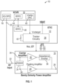
Figure 1 is a block diagram of a related-art power amplifier system having an envelope tracking integrated circuit (ETIC) and a barely Doherty power amplifier. -
Figure 2 is a block diagram showing a related-art basic barely Doherty power amplifier. -
Figure 3 is a diagram showing related art of a bias control of the peaking amplifier. -
Figure 4 is a diagram showing an embodiment in which the peaking amplifier bias (t) = f(Vcc peaking (t)) with the power supply voltage (Vcc) peaking in an ET modulated supply. -
Figure 5 is a diagram showing another embodiment in which each amplifier uses the ET modulated supply to modulate also the bias. -
Figure 6 is a diagram showing a bias network that maps ET Vcc into a bias modulation that is made programmable. -
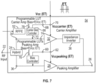
Figure 7 is a diagram showing both carrier and peaking amplifiers bias mapping to ET Vcc that are made programmable. -
Figures 8A and8B are diagrams showing the circuit topology of a barely Doherty ET differential amplifier using the modulated ET Vcc for peaking amplifier bias control. -
Figure 9 is a diagram showing a circuit topology of a barely Doherty ET differential amplifier using two independent ET Vccs, each applied also to its respective bias control. -
Figure 10 is a diagram showing a main embodiment showing direct current (DC) bias control, as a function of Pout, and modulated bias control using the modulated ET Vcc. -
Figure 11 is a diagram showing a main embodiment showing the two bias sums for the peaking amplifier. -
Figure 12 is a diagram showing a single DC bias programming and internal mapping to program the DC bias of the peaking amplifier from the carrier amplifier value. -
Figure 13 is a graph showing an example of peaking amplifier bias control represented by Ip/b relative to the modulated ET Vcc. -
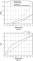
Figures 14 to 21 are graphs showing various ET barely Doherty signals. - The embodiments set forth below represent the necessary information to enable those skilled in the art to practice the embodiments and illustrate the best mode of practicing the embodiments. Upon reading the following description in light of the accompanying drawing figures, those skilled in the art will understand the concepts of the disclosure and will recognize applications of these concepts not particularly addressed herein. It should be understood that these concepts and applications fall within the scope of the disclosure and the accompanying claims.
- It will be understood that, although the terms first, second, etc. may be used herein to describe various elements, these elements should not be limited by these terms. These terms are only used to distinguish one element from another. For example, a first element could be termed a second element, and, similarly, a second element could be termed a first element, without departing from the scope of the present disclosure. As used herein, the term "and/or" includes any and all combinations of one or more of the associated listed items.
- It will be understood that when an element such as a layer, region, or substrate is referred to as being "on" or extending "onto" another element, it can be directly on or extend directly onto the other element or intervening elements may also be present. In contrast, when an element is referred to as being "directly on" or extending "directly onto" another element, there are no intervening elements present. Likewise, it will be understood that when an element such as a layer, region, or substrate is referred to as being "over" or extending "over" another element, it can be directly over or extend directly over the other element or intervening elements may also be present. In contrast, when an element is referred to as being "directly over" or extending "directly over" another element, there are no intervening elements present. It will also be understood that when an element is referred to as being "connected" or "coupled" to another element, it can be directly connected or coupled to the other element or intervening elements may be present. In contrast, when an element is referred to as being "directly connected" or "directly coupled" to another element, there are no intervening elements present.
- Relative terms such as "below" or "above" or "upper" or "lower" or "horizontal" or "vertical" may be used herein to describe a relationship of one element, layer, or region to another element, layer, or region as illustrated in the Figures. It will be understood that these terms and those discussed above are intended to encompass different orientations of the device in addition to the orientation depicted in the Figures.
- The terminology used herein is for the purpose of describing particular embodiments only and is not intended to be limiting of the disclosure. As used herein, the singular forms "a," "an," and "the" are intended to include the plural forms as well, unless the context clearly indicates otherwise. It will be further understood that the terms "comprises," "comprising," "includes," and/or "including" when used herein specify the presence of stated features, integers, steps, operations, elements, and/or components, but do not preclude the presence or addition of one or more other features, integers, steps, operations, elements, components, and/or groups thereof.
- Unless otherwise defined, all terms (including technical and scientific terms) used herein have the same meaning as commonly understood by one of ordinary skill in the art to which this disclosure belongs. It will be further understood that terms used herein should be interpreted as having a meaning that is consistent with their meaning in the context of this specification and the relevant art and will not be interpreted in an idealized or overly formal sense unless expressly so defined herein.
- Embodiments are described herein with reference to schematic illustrations of embodiments of the disclosure. As such, the actual dimensions of the layers and elements can be different, and variations from the shapes of the illustrations as a result, for example, of manufacturing techniques and/or tolerances, are expected. For example, a region illustrated or described as square or rectangular can have rounded or curved features, and regions shown as straight lines may have some irregularity. Thus, the regions illustrated in the figures are schematic and their shapes are not intended to illustrate the precise shape of a region of a device and are not intended to limit the scope of the disclosure. Additionally, sizes of structures or regions may be exaggerated relative to other structures or regions for illustrative purposes and, thus, are provided to illustrate the general structures of the present subject matter and may or may not be drawn to scale. Common elements between figures may be shown herein with common element numbers and may not be subsequently re-described.
- The present disclosure relates to a method to control the peaking amplifier of a load modulation power amplifier for a full or barely Doherty envelope tracking (ET) power amplifier.
-
Figure 1 is a schematic depicting a related-artpower amplifier system 10 having an envelope tracking integrated circuit (ETIC) 12, a DohertyET power amplifier 14, and a transceiver (XCVR) 16. TheETIC 12 is configured to supply the barely DohertyET power amplifier 14 with modulated power that tracks the envelope of a radio frequency (RF) signal generated by theXCVR 16. An in-phase/quadrature digital predistortion (I/Q DPD) 18 included in theXCVR 16 has apredistortion output 20 that is coupled to anRF input 22 of ahybrid coupler 24 included in the DohertyET power amplifier 14. The RF signal generated by theXCVR 16 is pre-distorted by the I/Q DPD 18 to improve linearity of an amplified version of the RF signal output from anRF output 26. A peakingamplifier 28 is coupled between afirst coupler output 30 and theRF output 26. Acarrier amplifier 32 is coupled in series between asecond coupler output 34 and animpedance inverter 36 coupled to theRF output 26. -
Tracker circuitry 38 included in theETIC 12 receives an analog signal Vcctarget that is generated by a Vramp digital-to-analog (DAC)converter 40. Vramp is a digital signal that follows the envelope of the RF signal being amplified by the DohertyET power amplifier 14. Thetracker circuitry 38 incorporates apower inductor 42 to filter an envelope tracked supply voltage VCC_ET. A first RF front-end (RFFE)interface 44 of theXCVR 16 is coupled to asecond RFFE interface 46 of theETIC 12. TheXCRV 16 is configured to send digital control signals and data between thefirst RFFE interface 44 and thesecond RFFE interface 46 to control theETIC 12. The digital control signals include but are not limited to switching RF bands and controlling power levels. -
Figure 2 shows a basic simplified schematic of the related-artDoherty power amplifier 14 and defined baseband parameters. This simple model of the radio frequency (RF) voltages and currents of the Doherty power amplifier, which is of the load-line modulation type, includes the peakingamplifier 28 and thecarrier amplifier 32. The envelope of the RF voltage across thecarrier amplifier 32 is designated Vm, and the associated baseband current is designated Im. The envelope of the RF voltage across the peaking amplifier is designated Vp, and the associated baseband current is designated j*Ip, wherein j2 = -1. - The
impedance inverter 34 having an impedance inverter coefficient Ka is a block that makes Zin*ZL = -Ka2, with Ka = j∗|Ka|, with |Ka| = 2∗ZL for the barelyDoherty power amplifier 14, and Zin and ZL are the impedance at theRF input 22 and theRF output 26, respectively, of theimpedance inverter 34. The impedance inverter coefficient Ka equals a value of characteristic impedance Z0 that provides impedance inversion between an input and an output of theimpedance inverter 34. - In a related-art diagram of a load modulation mainly in average power tracking (APT) mode,
Figure 3 shows the related-art DohertyET power amplifier 14 with dynamic power amplifier bias (DPAB)control circuitry 48 that is configured to controlbias circuitry 50 of the peakingamplifier 28. In operation, theDPAB control circuity 48 activates thebias circuitry 50 to bias the peakingamplifier 28 from one class of operation to another class of operation during the modulation envelope ET. TheDPAB control circuitry 48 that responds to the detected envelope of the modulation envelope ET at a base of thecarrier amplifier 32 and couples detected envelope to thebias circuitry 50 of the peakingamplifier 28 and thereby increasing or decreasing the class of operation of the peaking amplifier. TheDPAB control circuity 48 is also known as a fast bias-debias controller. - In a barely ET Doherty power amplifier, in related art, the circuit DPAB is disabled, and both the peaking
amplifier 28 and thecarrier amplifier 28 are operating in class AB, and no bias changes are done on the peakingamplifier 28. Athird RFFE interface 52 is included to allow changes to amplifier parameters such as power level control during operation of the related-art DohertyET power amplifier 14. - A method according to the present disclosure uses the modulated power supply voltage (Vcc) signal that changes vs. the modulation envelope for isogain operation, for example, to control the bias of the peaking amplifier where the modulated ET Vcc signal is adjusting and changing the class of operation of the peaking amplifier, and thus allowing improved efficiency and reduced memory effects without the need to detect wide modulation envelope. Basically, the peaking amplifier modulated bias is a function of the ET supply modulation signal, that is, peaking amplifier bias (t) = f(Vcc (t)). This allows the peaking amplifier to operate in Class C at low power level and quickly bias/debias when load modulation is applied using the same modulation ET Vcc signal, such that both ET Vcc and the bias modulation move at the same rate and change at the same time.
-
Figure 4 shows an example embodiment of a barely DohertyET power amplifier 54 in which the peaking amplifier bias (t) = f(Vcc peaking (t)) with the Vcc peaking in an ET modulated supply. In this example embodiment, thecarrier amplifier 32 hastraditional bias circuitry 56, while bias to the peakingamplifier 28 is controlled by a peakingbias controller 58. The peakingbias controller 58 has a peakingbias control input 60 coupled to a peakingsupply node 62 and a peakingbias control output 64 coupled to a peakingbias input 65. In operation, the peakingbias controller 58 generates a modulated peaking bias signal that controls bias of the peakingamplifier 28 in response to a modulated peaking supply voltage at the peakingsupply node 62. -
Figure 5 is a schematic of another example embodiment of the barelyDoherty power amplifier 54. In this embodiment, the barelyDoherty power amplifier 54 includes acarrier bias controller 66 having a carrierbias control input 68 coupled to acarrier supply node 70 and a carrierbias control output 72 coupled to acarrier bias input 74. In operation, thecarrier bias controller 66 generates a modulated carrier bias signal that controls bias of thecarrier amplifier 32 in response to a modulated carrier supply voltage at thecarrier supply node 70. As a result of this example embodiment, the respective bias of both thecarrier amplifier 32 and the peakingamplifier 28 are modulated by the modulated ET Vcc supply voltage. - The peaking
bias controller 58 is made programmable to map a given ET Vcc voltage into a given bias response by way of a first programmable analog look-up table (LUT) 76, as shown inFigure 6 . This example embodiment can be extended to control biases of both thecarrier amplifier 32 and the peakingamplifier 28 by adding a second programmable analog LUT 78, as shown inFigure 7 . The second programmable analog LUT may also be referred to as a carrier look-up table. -
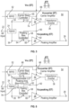
Figure 8A is a schematic of an example embodiment of a differential barelyET Doherty amplifier 80 using the modulated ET Vcc for bias modulation. The differential barelyDoherty power amplifier 80, which is of the load-line modulation type, includes adifferential peaking amplifier 82 and adifferential carrier amplifier 84. A 0°/90°hybrid coupler 86 has anRF input 88,first coupler input 90, and asecond coupler output 92. Thedifferential peaking amplifier 82 is coupled between thefirst coupler output 90 and a primary 94 of anRF transformer 96. Thedifferential carrier amplifier 84 is coupled between thesecond coupler output 92 and adifferential impedance inverter 98, which is coupled between thedifferential carrier amplifier 84 and the primary 94. Afilter 100 and aload 102 are coupled across a secondary 104 of theRF transformer 96. A differentialpeaking bias controller 106 has a differential peakingbias control input 108 coupled to aprimary tap 110 and a differential peakingbias control output 112 coupled to a differentialpeaking bias input 114. In operation, the peakingbias controller 106 generates a modulated peaking bias signal that controls bias of thedifferential peaking amplifier 82 in response to a modulated peaking supply voltage at theprimary tap 110. In operation, the differentialpeaking bias controller 106 generates a modulated peaking bias signal that controls bias of thedifferential peaking amplifier 82 in response to a modulated peaking supply voltage Vcc (ET) at theprimary tap 110. -
Figure 8B is a schematic of another version of the example embodiment of the differential barelyET Doherty amplifier 80 using the modulated ET Vcc for bias modulation of thedifferential peaking amplifier 82. In this case, thedifferential peaking amplifier 82 is coupled to a peakingtransformer 116 and thedifferential carrier amplifier 84 is coupled to acarrier transformer 118. Also, in this case, theimpedance inverter 98 is coupled between a secondary 120 of thecarrier transformer 118 and thefilter 100. Furthermore, the differential peakingbias control input 108 is coupled to a commonprimary tap 122. A secondary 124 of the peakingtransformer 116 is coupled across thefilter 100 and theload 104. In operation, the differentialpeaking bias controller 106 generates a modulated peaking bias signal that controls bias of thedifferential peaking amplifier 82 in response to a modulated peaking supply voltage Vcc (ET) at the commonprimary tap 122. -
Figure 9 is a schematic showing an embodiment showing separate ET Vcc, one for thedifferential carrier amplifier 84 and one for thedifferential peaking amplifier 82, with bias control modulation using their respective ET Vcc modulations. In this case, acarrier bias controller 126 has a differential carrierbias control input 128 that is coupled to a carrier supply node labeled Vcc Carrier (ET/APT) and a differential carrierbias control output 130 coupled to acarrier bias input 132. Also, the differential peakingbias control input 108 is coupled to a peaking supply node labeled Vcc Peaking (ET/APT). - In operation, the differential
peaking bias controller 106 generates a modulated peaking bias signal that controls bias of thedifferential peaking amplifier 82 in response to the modulated peaking supply voltage Vcc (ET/APT) at the commonprimary tap 122. Moreover, the differentialcarrier bias controller 116 generates a modulated peaking bias signal that controls bias of thedifferential carrier amplifier 84 in response to the modulated carrier supply voltage Vcc (ET). -
Figure 10 is schematic of another version of the example embodiment of the differential barelyET Doherty amplifier 80 in which the peakingbias controller 106 includes a peakingDC bias input 134. The peakingbias controller 106 is further configured to add DC bias control to thedifferential peaking amplifier 82 as a function of average output power (Avg Pout). Thecarrier bias controller 126 includes a carrier DC biasinput 136. Thecarrier bias controller 126 is further configured to control the bias of thedifferential carrier amplifier 84 as a function of average output power (Avg Pout). -
Figure 11 is schematic of a version of the example embodiment of the differential barelyET Doherty amplifier 80 in which the peakingbias controller 106 is not configured to add DC bias control to thedifferential peaking amplifier 82. Instead, a separate peakingDC bias controller 140 having aDC bias input 142 is further configured to control the bias of thedifferential peaking amplifier 82 as a function of average output power (Avg Pout). The peaking amplifier bias control is thus the sum of a DC bias control programmed via thethird RFFE interface 52 that is function of Pout and a modulated bias using the modulated ET Vcc, which slope can be also programmable via thethird RFFE interface 52, as shown inFigure 11 . - One also may consider the embodiment in
Figure 12 , in which thethird RFFE interface 52 only programs one DC bias value that is a function of Pout and that is used to adjust the bias for the carrier amplifier, similar to any other type of power amplifier. Then internally, an analog or digital map to the corresponding DC bias value is made for the peaking amplifier using an analog or digital LUT stored withinDC bias mapping 144, which can be adjustable via thethird RFFE interface 52 if needed, and thus only requiring the programming versus total power control changes of one DC bias value and thus maintaining compatibility with all other types of power amplifiers, as shown inFigure 12 . Changes in DC bias corresponding to DC bias values selected from theDC bias mapping 144 are conveyed through the DC biasinput 142. Selections of DC bias values are a function of peaking DC bias slope transmitted through a biasslope terminal input 146. Selections of DC bias values may also be made through an average outputpower input terminal 148. -
Figure 13 shows an example of peaking amplifier bias control represented by Ip/b relative to the modulated ET Vcc, which is labeled Vm inFigure 13 .Figures 14 to 21 show various ET barely Doherty signals. - An advantage of the disclosed embodiments is that the peaking amplifier bias control is based on two components:
- one DC bias control that is adjustable via the radio frequency front-end (RFFE) to adjust the DC bias versus average output power change, and
- a modulated bias control that uses the modulated ET Vcc, which relation relative to ET Vcc can be made programmable via RFFE programming. Note that the embodiments are configured to handle wide bandwidth modulation to avoid creating memory effects.
- It is contemplated that any of the foregoing aspects, and/or various separate aspects and features as described herein, may be combined for additional advantage. Any of the various embodiments as disclosed herein may be combined with one or more other disclosed embodiments unless indicated to the contrary herein.
- Those skilled in the art will recognize improvements and modifications to the illustrative embodiments of the present disclosure. All such improvements and modifications are considered within the scope of the concepts disclosed herein and the claims that follow.
- Therefore, from one perspective, there has been described a power amplifier system with a carrier amplifier having a carrier bias input and a carrier supply node and a peaking amplifier having a peaking bias input and a peaking supply node. Also included is an envelope tracking power supply having a modulated voltage supply output coupled to the peaking supply node. Further included is a peaking bias controller having a peaking bias control input coupled to the peaking supply node and a peaking bias control output coupled to the peaking bias input, wherein the peaking bias controller is configured to generate in response to a modulated peaking supply voltage generated by the envelope tracking power supply at the peaking supply node a modulated peaking bias signal that controls bias of the peaking amplifier.
- Further examples are set out the following numbered clauses:
-
Clause 1. A power amplifier system comprising: a carrier amplifier having a carrier bias input and a carrier supply node; a peaking amplifier having a peaking bias input and a peaking supply node; an envelope tracking power supply having a modulated voltage supply output coupled to the peaking supply node; and a peaking bias controller having a peaking bias control input coupled to the peaking supply node and a peaking bias control output coupled to the peaking bias input, wherein the peaking bias controller generates in response to a modulated peaking supply voltage generated by the envelope tracking power supply at the peaking supply node a modulated peaking bias signal that controls bias of the peaking amplifier. -
Clause 2. The power amplifier system ofclause 1 wherein the peaking bias controller comprises a peaking look-up table having direct current peaking bias values that correspond with instantaneous levels of the modulated peaking supply voltage. -
Clause 3. The power amplifier system ofclause 2 wherein the direct current peaking bias values correspond to the modulated peaking voltage nonlinearly. -
Clause 4. The power amplifier system ofclause -
Clause 5. The power amplifier system ofclause 4 wherein the peaking digital interface is coupled to a radio frequency front-end (RFFE) control interface. -
Clause 6. The power amplifier system of any ofclauses 2 to 5 wherein the peaking bias controller comprises: a peaking analog-to-digital converter having a peaking analog input coupled to the peaking bias control input and a peaking digital output; the peaking look-up table having a peaking look-up input coupled to the peaking digital output and a peaking look-up output; and a peaking digital-to-analog converter having a peaking digital input coupled to the peaking look-up output and a peaking analog output coupled to the peaking bias control output. - Clause 7. The power amplifier system of any preceding clause further comprising a carrier bias controller having a carrier bias control input coupled to the carrier supply node and a carrier bias control output coupled to the carrier bias input, wherein the carrier bias controller generates in response to a modulated carrier supply voltage generated by the envelope tracking power supply at the carrier supply node a modulated carrier bias signal that controls bias of the carrier amplifier.
-
Clause 8. The power amplifier system of clause 7 wherein the carrier bias controller comprises a carrier look-up table having direct current carrier bias values that correspond with instantaneous levels of the modulated carrier supply voltage. -
Clause 9. The power amplifier system ofclause 8 wherein the direct current carrier bias values correspond to the modulated carrier voltage nonlinearly. -
Clause 10. The power amplifier system ofclause -
Clause 11. The power amplifier system ofclause 10 wherein the carrier digital interface is coupled to the RFFE control interface. -
Clause 12. The power amplifier system of any of clauses 7 to 11 wherein the modulated peaking bias signal that controls bias of the peaking amplifier has a modulation bandwidth that is between 400 MHz and 500 MHz. - Clause 13. The power amplifier system of any of clauses 7 to 12 wherein the carrier bias controller comprises: a carrier analog-to-digital converter having a carrier analog input coupled to the carrier bias control input and a carrier digital output; a carrier look-up table having a carrier look-up input coupled to the carrier digital output and a carrier look-up output; and a carrier digital-to-analog converter having a carrier digital input coupled to the carrier look-up output and a carrier analog output coupled to the carrier bias control output.
-
Clause 14. The power amplifier system of any preceding clause wherein the peaking amplifier and the carrier amplifier are configured as differential amplifiers. -
Clause 15. The power amplifier system of any preceding clause wherein the envelope tracking power supply is configured to supply the carrier amplifier with an average power tracking (APT) modulated supply voltage. -
Clause 16. The power amplifier system of any preceding clause wherein the envelope tracking power supply is configured to supply the peaking amplifier with APT modulated supply voltage. - Clause 17. The power amplifier system of any preceding clause wherein the envelope tracking power supply is configured to supply the carrier amplifier with instantaneous envelope tracking modulated voltage.
-
Clause 18. The power amplifier system of any preceding clause wherein the envelope tracking power supply is configured to supply the peaking amplifier with instantaneous envelope tracking modulated voltage. - Clause 19. The power amplifier system of
clause 18 further comprising a peaking direct current (DC) bias control coupled between the modulated voltage supply output and the peaking bias input, wherein the peaking DC bias control is configured to adjust DC bias of the peaking amplifier as a function of average output power of the peaking amplifier. -
Clause 20. The power amplifier system ofclause 18 or 19 further comprising a carrier direct current (DC) bias control coupled between the modulated voltage supply output and the carrier bias input, wherein the carrier DC bias control is configured to adjust DC bias of the carrier amplifier as a function of average output power of the carrier amplifier. - Clause 21. The power amplifier system of
clause -
Clause 22. The power amplifier system of clause 21 wherein the DC bias mapping look-up table is programmable over the RFFE control interface. - Clause 23. The power amplifier system of any of clauses 19 to 22 wherein the carrier DC bias control and the peaking DC bias control are configured to receive average power output values that are proportional to the combined power output of the carrier amplifier and the peaking amplifier, wherein the carrier DC bias control and the peaking DC bias control are configured to control the carrier DC bias and the peaking DC bias in response to the average power output values.
-
Clause 24. The power amplifier system of clause 23 wherein the average power output values are transmitted to the carrier DC bias control and the peaking DC bias control over the RFFE control interface.
Claims (15)
- A power amplifier system comprising:• a carrier amplifier having a carrier bias input and a carrier supply node;• a peaking amplifier having a peaking bias input and a peaking supply node;• an envelope tracking power supply having a modulated voltage supply output coupled to the peaking supply node; and• a peaking bias controller having a peaking bias control input coupled to the peaking supply node and a peaking bias control output coupled to the peaking bias input, wherein the peaking bias controller generates in response to a modulated peaking supply voltage generated by the envelope tracking power supply at the peaking supply node a modulated peaking bias signal that controls bias of the peaking amplifier.
- The power amplifier system of claim 1 wherein the peaking bias controller comprises a peaking look-up table having direct current peaking bias values that correspond with instantaneous levels of the modulated peaking supply voltage, and for example wherein the direct current peaking bias values correspond to the modulated peaking voltage nonlinearly.
- The power amplifier system of claim 2 further comprising a peaking digital interface coupled to the peaking look-up table, wherein the peaking look-up table is programmable to receive new direct current peaking bias values over the peaking digital interface, and for example wherein the peaking digital interface is coupled to a radio frequency front-end (RFFE) control interface.
- The power amplifier system of 2 or 3 wherein the peaking bias controller comprises:• a peaking analog-to-digital converter having a peaking analog input coupled to the peaking bias control input and a peaking digital output;• the peaking look-up table having a peaking look-up input coupled to the peaking digital output and a peaking look-up output; and• a peaking digital-to-analog converter having a peaking digital input coupled to the peaking look-up output and a peaking analog output coupled to the peaking bias control output.
- The power amplifier system of any preceding claim further comprising a carrier bias controller having a carrier bias control input coupled to the carrier supply node and a carrier bias control output coupled to the carrier bias input, wherein the carrier bias controller generates in response to a modulated carrier supply voltage generated by the envelope tracking power supply at the carrier supply node a modulated carrier bias signal that controls bias of the carrier amplifier.
- The power amplifier system of claim 5 wherein the carrier bias controller comprises a carrier look-up table having direct current carrier bias values that correspond with instantaneous levels of the modulated carrier supply voltage, and for example wherein the direct current carrier bias values correspond to the modulated carrier voltage nonlinearly.
- The power amplifier system of claim 6 further comprising a carrier digital interface coupled to the carrier look-up table, wherein the carrier look-up table is programmable to receive new direct current carrier bias values over the carrier digital interface, and for example wherein the carrier digital interface is coupled to the RFFE control interface.
- The power amplifier system of any of claims 5 to 7 wherein the modulated peaking bias signal that controls bias of the peaking amplifier has a modulation bandwidth that is between 400 MHz and 500 MHz.
- The power amplifier system of any of claims 5 to 8 wherein the carrier bias controller comprises:• a carrier analog-to-digital converter having a carrier analog input coupled to the carrier bias control input and a carrier digital output;• a carrier look-up table having a carrier look-up input coupled to the carrier digital output and a carrier look-up output; and• a carrier digital-to-analog converter having a carrier digital input coupled to the carrier look-up output and a carrier analog output coupled to the carrier bias control output.
- The power amplifier system of any preceding claim wherein the envelope tracking power supply is configured to supply the carrier amplifier with an average power tracking (APT) modulated supply voltage, and for example is configured to supply the peaking amplifier with APT modulated supply voltage.
- The power amplifier system of any preceding claim wherein the envelope tracking power supply is configured to supply one or more of the carrier amplifier with and the peaking amplifier with instantaneous envelope tracking modulated voltage.
- The power amplifier system of claim 11 further comprising a peaking direct current (DC) bias control coupled between the modulated voltage supply output and the peaking bias input, wherein the peaking DC bias control is configured to adjust DC bias of the peaking amplifier as a function of average output power of the peaking amplifier.
- The power amplifier system of claim 11 or 12 further comprising a carrier direct current (DC) bias control coupled between the modulated voltage supply output and the carrier bias input, wherein the carrier DC bias control is configured to adjust DC bias of the carrier amplifier as a function of average output power of the carrier amplifier.
- The power amplifier system of any of claims 11 to 13 further comprising a DC bias mapping look-up table coupled to the peaking DC bias, wherein the DC bias mapping look-up table is configured to adjust slope of the peaking bias control, and for example is programmable over the RFFE control interface.
- The power amplifier system of claim 13 or 14 wherein the carrier DC bias control and the peaking DC bias control are configured to receive average power output values that are proportional to the combined power output of the carrier amplifier and the peaking amplifier, wherein the carrier DC bias control and the peaking DC bias control are configured to control the carrier DC bias and the peaking DC bias in response to the average power output values, and for example wherein the average power output values are transmitted to the carrier DC bias control and the peaking DC bias control over the RFFE control interface.
Applications Claiming Priority (2)
| Application Number | Priority Date | Filing Date | Title |
|---|---|---|---|
| US202263305471P | 2022-02-01 | 2022-02-01 | |
| US17/872,140 US12587140B2 (en) | 2022-02-01 | 2022-07-25 | Barely Doherty et using et VCC modulation for bias control |
Publications (1)
| Publication Number | Publication Date |
|---|---|
| EP4220948A1 true EP4220948A1 (en) | 2023-08-02 |
Family
ID=85158651
Family Applications (1)
| Application Number | Title | Priority Date | Filing Date |
|---|---|---|---|
| EP23154372.9A Pending EP4220948A1 (en) | 2022-02-01 | 2023-02-01 | Barely doherty et using et vcc modulation for bias control |
Country Status (2)
| Country | Link |
|---|---|
| US (1) | US12587140B2 (en) |
| EP (1) | EP4220948A1 (en) |
Cited By (1)
| Publication number | Priority date | Publication date | Assignee | Title |
|---|---|---|---|---|
| WO2026024380A1 (en) * | 2024-07-23 | 2026-01-29 | Qorvo Us, Inc. | Controlling a dual-amplifier power amplifier circuit in a power management circuit |
Families Citing this family (2)
| Publication number | Priority date | Publication date | Assignee | Title |
|---|---|---|---|---|
| WO2023068266A1 (en) * | 2021-10-20 | 2023-04-27 | 株式会社村田製作所 | Power amplifying circuit and power amplifying device |
| US12603614B2 (en) * | 2022-12-09 | 2026-04-14 | Silicon Laboratories Inc. | Wideband doherty power amplifier |
Citations (3)
| Publication number | Priority date | Publication date | Assignee | Title |
|---|---|---|---|---|
| US20150295541A1 (en) * | 2014-04-09 | 2015-10-15 | Qualcomm Incorporated | Circuits and methods for biasing a power amplifier |
| US20150318827A1 (en) * | 2014-04-30 | 2015-11-05 | Freescale Semiconductor, Inc. | Power amplifier with envelope injection |
| US20170257068A1 (en) * | 2016-03-02 | 2017-09-07 | Qualcomm Incorporated | Systems and methods for linearizing operation of a power amplifier |
Family Cites Families (17)
| Publication number | Priority date | Publication date | Assignee | Title |
|---|---|---|---|---|
| US20020146993A1 (en) * | 2001-04-04 | 2002-10-10 | Charles Persico | Bias adjustment for power amplifier |
| KR100553252B1 (en) | 2002-02-01 | 2006-02-20 | 아바고테크놀로지스코리아 주식회사 | Power amplifier of portable terminal |
| KR20100069454A (en) | 2008-12-16 | 2010-06-24 | 삼성전자주식회사 | Method and apparatus for enhancing performance of a doherty power amplifier in a communication system |
| US9531327B2 (en) | 2012-10-31 | 2016-12-27 | Nec Corporation | Power amplifier and power amplification method |
| JP2014175760A (en) | 2013-03-07 | 2014-09-22 | Japan Radio Co Ltd | Asymmetric Doherty power amplifier |
| KR101500570B1 (en) | 2013-06-26 | 2015-03-09 | 주식회사 인스파워 | Asymmetric Doherty Amplifier |
| US9225291B2 (en) | 2013-10-29 | 2015-12-29 | Freescale Semiconductor, Inc. | Adaptive adjustment of power splitter |
| US9252722B2 (en) | 2013-12-20 | 2016-02-02 | Telefonaktiebolaget L M Ericsson (Publ) | Enhanced and versatile N-way doherty power amplifier |
| EP3236583A4 (en) | 2014-12-18 | 2018-08-01 | Kabushiki Kaisha Toshiba | Doherty amplifier |
| JP2018137566A (en) | 2017-02-21 | 2018-08-30 | 株式会社村田製作所 | Power amplifier circuit |
| US11165393B2 (en) | 2019-03-25 | 2021-11-02 | Skyworks Solutions, Inc. | Envelope tracking for Doherty power amplifiers |
| DE112019007775T5 (en) | 2019-10-02 | 2022-06-15 | Mitsubishi Electric Corporation | Doherty amplifier |
| US20210167735A1 (en) | 2019-12-02 | 2021-06-03 | Nxp Usa, Inc. | Doherty power amplifiers with improved peaking amplifier matching |
| CN114747136B (en) | 2019-12-13 | 2025-04-15 | 三菱电机株式会社 | Doherty amplifier and communication device |
| JP2021192476A (en) * | 2020-06-05 | 2021-12-16 | 株式会社村田製作所 | Power amplifier circuit |
| US11190147B1 (en) | 2020-06-18 | 2021-11-30 | Silicon Laboratories Inc. | Low power, efficient doherty power amplifier |
| US12413190B2 (en) | 2021-08-16 | 2025-09-09 | Skyworks Solutions, Inc. | Power amplifier supply networks with harmonic terminations |
-
2022
- 2022-07-25 US US17/872,140 patent/US12587140B2/en active Active
-
2023
- 2023-02-01 EP EP23154372.9A patent/EP4220948A1/en active Pending
Patent Citations (3)
| Publication number | Priority date | Publication date | Assignee | Title |
|---|---|---|---|---|
| US20150295541A1 (en) * | 2014-04-09 | 2015-10-15 | Qualcomm Incorporated | Circuits and methods for biasing a power amplifier |
| US20150318827A1 (en) * | 2014-04-30 | 2015-11-05 | Freescale Semiconductor, Inc. | Power amplifier with envelope injection |
| US20170257068A1 (en) * | 2016-03-02 | 2017-09-07 | Qualcomm Incorporated | Systems and methods for linearizing operation of a power amplifier |
Non-Patent Citations (3)
| Title |
|---|
| "Doherty amplifier with cooperative power tracking and bias adaption for high efficiency", RESEARCH DISCLOSURE, KENNETH MASON PUBLICATIONS, HAMPSHIRE, UK, GB, vol. 578, no. 37, 2 June 2012 (2012-06-02), pages 453, XP007141360, ISSN: 0374-4353 * |
| RYU NAMSIK ET AL: "CMOS Doherty Amplifier With Variable Balun Transformer and Adaptive Bias Control for Wireless LAN Application", IEEE JOURNAL OF SOLID-STATE CIRCUITS, IEEE, USA, vol. 49, no. 6, 2 June 2014 (2014-06-02), pages 1356 - 1365, XP011549316, ISSN: 0018-9200, [retrieved on 20140528], DOI: 10.1109/JSSC.2014.2313561 * |
| YONG-SUB LEE ET AL: "Highly linear and efficient Doherty amplifier employing power tracking bias supply scheme for WCDMA applications", RADIO AND WIRELESS SYMPOSIUM, 2008 IEEE, IEEE, PISCATAWAY, NJ, USA, 22 January 2008 (2008-01-22), pages 73 - 76, XP031237101, ISBN: 978-1-4244-1462-8 * |
Cited By (1)
| Publication number | Priority date | Publication date | Assignee | Title |
|---|---|---|---|---|
| WO2026024380A1 (en) * | 2024-07-23 | 2026-01-29 | Qorvo Us, Inc. | Controlling a dual-amplifier power amplifier circuit in a power management circuit |
Also Published As
| Publication number | Publication date |
|---|---|
| US12587140B2 (en) | 2026-03-24 |
| US20230246596A1 (en) | 2023-08-03 |
Similar Documents
| Publication | Publication Date | Title |
|---|---|---|
| US12587140B2 (en) | Barely Doherty et using et VCC modulation for bias control | |
| CN101702618B (en) | Gain control of radio frequency linear power amplifier | |
| US10038461B2 (en) | RF amplifier having a transition shaping filter | |
| US6734724B1 (en) | Power control and modulation of switched-mode power amplifiers with one or more stages | |
| EP1262018B1 (en) | High-efficiency power modulators | |
| US11588449B2 (en) | Envelope tracking power amplifier apparatus | |
| US8301088B2 (en) | Polar modulation transmitter with envelope modulator path switching | |
| CN103812454B (en) | The calibration method and device of envelope tracing system | |
| US20220278651A1 (en) | Barely doherty dual envelope tracking (bd2e) circuit | |
| US9813088B2 (en) | Supply modulators with voltage and frequency partitioning | |
| US12267046B2 (en) | Power amplifier system | |
| CN100517960C (en) | Amplifiers, and transmitters and communication devices using the amplifiers | |
| CN101095280A (en) | Multi-state load switched power amplifier for polar modulation transmitter | |
| US8346185B2 (en) | Method and system for enhancing efficiency by modulating power amplifier gain | |
| JP2005045440A (en) | Power amplifier and wireless communication apparatus using the same | |
| CN107222174A (en) | A kind of low-loss adaptive bias circuit and wireless transmitting system | |
| US20250150046A1 (en) | Hybrid power amplifier circuit | |
| CN116545387A (en) | Rare Doherty ET Using ETVCC Modulation for Bias Control | |
| CN1938956A (en) | Radio transmitter with reduced power consumption |
Legal Events
| Date | Code | Title | Description |
|---|---|---|---|
| PUAI | Public reference made under article 153(3) epc to a published international application that has entered the european phase |
Free format text: ORIGINAL CODE: 0009012 |
|
| STAA | Information on the status of an ep patent application or granted ep patent |
Free format text: STATUS: THE APPLICATION HAS BEEN PUBLISHED |
|
| AK | Designated contracting states |
Kind code of ref document: A1 Designated state(s): AL AT BE BG CH CY CZ DE DK EE ES FI FR GB GR HR HU IE IS IT LI LT LU LV MC ME MK MT NL NO PL PT RO RS SE SI SK SM TR |
|
| STAA | Information on the status of an ep patent application or granted ep patent |
Free format text: STATUS: REQUEST FOR EXAMINATION WAS MADE |
|
| 17P | Request for examination filed |
Effective date: 20240202 |
|
| RBV | Designated contracting states (corrected) |
Designated state(s): AL AT BE BG CH CY CZ DE DK EE ES FI FR GB GR HR HU IE IS IT LI LT LU LV MC ME MK MT NL NO PL PT RO RS SE SI SK SM TR |