EP4220736B1 - Transistor - Google Patents
Transistor Download PDFInfo
- Publication number
- EP4220736B1 EP4220736B1 EP23153062.7A EP23153062A EP4220736B1 EP 4220736 B1 EP4220736 B1 EP 4220736B1 EP 23153062 A EP23153062 A EP 23153062A EP 4220736 B1 EP4220736 B1 EP 4220736B1
- Authority
- EP
- European Patent Office
- Prior art keywords
- layer
- oxide semiconductor
- transistor
- semiconductor layer
- gate electrode
- Prior art date
- Legal status (The legal status is an assumption and is not a legal conclusion. Google has not performed a legal analysis and makes no representation as to the accuracy of the status listed.)
- Active
Links
Images





Classifications
-
- H—ELECTRICITY
- H10—SEMICONDUCTOR DEVICES; ELECTRIC SOLID-STATE DEVICES NOT OTHERWISE PROVIDED FOR
- H10D—INORGANIC ELECTRIC SEMICONDUCTOR DEVICES
- H10D30/00—Field-effect transistors [FET]
- H10D30/60—Insulated-gate field-effect transistors [IGFET]
- H10D30/67—Thin-film transistors [TFT]
- H10D30/674—Thin-film transistors [TFT] characterised by the active materials
- H10D30/6741—Group IV materials, e.g. germanium or silicon carbide
-
- H—ELECTRICITY
- H10—SEMICONDUCTOR DEVICES; ELECTRIC SOLID-STATE DEVICES NOT OTHERWISE PROVIDED FOR
- H10D—INORGANIC ELECTRIC SEMICONDUCTOR DEVICES
- H10D30/00—Field-effect transistors [FET]
- H10D30/60—Insulated-gate field-effect transistors [IGFET]
- H10D30/67—Thin-film transistors [TFT]
- H10D30/6704—Thin-film transistors [TFT] having supplementary regions or layers in the thin films or in the insulated bulk substrates for controlling properties of the device
-
- H—ELECTRICITY
- H10—SEMICONDUCTOR DEVICES; ELECTRIC SOLID-STATE DEVICES NOT OTHERWISE PROVIDED FOR
- H10D—INORGANIC ELECTRIC SEMICONDUCTOR DEVICES
- H10D30/00—Field-effect transistors [FET]
- H10D30/60—Insulated-gate field-effect transistors [IGFET]
- H10D30/67—Thin-film transistors [TFT]
- H10D30/6704—Thin-film transistors [TFT] having supplementary regions or layers in the thin films or in the insulated bulk substrates for controlling properties of the device
- H10D30/6713—Thin-film transistors [TFT] having supplementary regions or layers in the thin films or in the insulated bulk substrates for controlling properties of the device characterised by the properties of the source or drain regions, e.g. compositions or sectional shapes
-
- H—ELECTRICITY
- H10—SEMICONDUCTOR DEVICES; ELECTRIC SOLID-STATE DEVICES NOT OTHERWISE PROVIDED FOR
- H10D—INORGANIC ELECTRIC SEMICONDUCTOR DEVICES
- H10D30/00—Field-effect transistors [FET]
- H10D30/60—Insulated-gate field-effect transistors [IGFET]
- H10D30/67—Thin-film transistors [TFT]
- H10D30/6729—Thin-film transistors [TFT] characterised by the electrodes
-
- H—ELECTRICITY
- H10—SEMICONDUCTOR DEVICES; ELECTRIC SOLID-STATE DEVICES NOT OTHERWISE PROVIDED FOR
- H10D—INORGANIC ELECTRIC SEMICONDUCTOR DEVICES
- H10D30/00—Field-effect transistors [FET]
- H10D30/60—Insulated-gate field-effect transistors [IGFET]
- H10D30/67—Thin-film transistors [TFT]
- H10D30/6729—Thin-film transistors [TFT] characterised by the electrodes
- H10D30/673—Thin-film transistors [TFT] characterised by the electrodes characterised by the shapes, relative sizes or dispositions of the gate electrodes
- H10D30/6733—Multi-gate TFTs
-
- H—ELECTRICITY
- H10—SEMICONDUCTOR DEVICES; ELECTRIC SOLID-STATE DEVICES NOT OTHERWISE PROVIDED FOR
- H10D—INORGANIC ELECTRIC SEMICONDUCTOR DEVICES
- H10D30/00—Field-effect transistors [FET]
- H10D30/60—Insulated-gate field-effect transistors [IGFET]
- H10D30/67—Thin-film transistors [TFT]
- H10D30/6729—Thin-film transistors [TFT] characterised by the electrodes
- H10D30/673—Thin-film transistors [TFT] characterised by the electrodes characterised by the shapes, relative sizes or dispositions of the gate electrodes
- H10D30/6735—Thin-film transistors [TFT] characterised by the electrodes characterised by the shapes, relative sizes or dispositions of the gate electrodes having gates fully surrounding the channels, e.g. gate-all-around
-
- H—ELECTRICITY
- H10—SEMICONDUCTOR DEVICES; ELECTRIC SOLID-STATE DEVICES NOT OTHERWISE PROVIDED FOR
- H10D—INORGANIC ELECTRIC SEMICONDUCTOR DEVICES
- H10D30/00—Field-effect transistors [FET]
- H10D30/60—Insulated-gate field-effect transistors [IGFET]
- H10D30/67—Thin-film transistors [TFT]
- H10D30/6729—Thin-film transistors [TFT] characterised by the electrodes
- H10D30/6737—Thin-film transistors [TFT] characterised by the electrodes characterised by the electrode materials
- H10D30/6739—Conductor-insulator-semiconductor electrodes
-
- H—ELECTRICITY
- H10—SEMICONDUCTOR DEVICES; ELECTRIC SOLID-STATE DEVICES NOT OTHERWISE PROVIDED FOR
- H10D—INORGANIC ELECTRIC SEMICONDUCTOR DEVICES
- H10D30/00—Field-effect transistors [FET]
- H10D30/60—Insulated-gate field-effect transistors [IGFET]
- H10D30/67—Thin-film transistors [TFT]
- H10D30/674—Thin-film transistors [TFT] characterised by the active materials
- H10D30/6755—Oxide semiconductors, e.g. zinc oxide, copper aluminium oxide or cadmium stannate
-
- H—ELECTRICITY
- H10—SEMICONDUCTOR DEVICES; ELECTRIC SOLID-STATE DEVICES NOT OTHERWISE PROVIDED FOR
- H10D—INORGANIC ELECTRIC SEMICONDUCTOR DEVICES
- H10D30/00—Field-effect transistors [FET]
- H10D30/60—Insulated-gate field-effect transistors [IGFET]
- H10D30/67—Thin-film transistors [TFT]
- H10D30/6757—Thin-film transistors [TFT] characterised by the structure of the channel, e.g. transverse or longitudinal shape or doping profile
-
- H—ELECTRICITY
- H10—SEMICONDUCTOR DEVICES; ELECTRIC SOLID-STATE DEVICES NOT OTHERWISE PROVIDED FOR
- H10D—INORGANIC ELECTRIC SEMICONDUCTOR DEVICES
- H10D62/00—Semiconductor bodies, or regions thereof, of devices having potential barriers
- H10D62/80—Semiconductor bodies, or regions thereof, of devices having potential barriers characterised by the materials
- H10D62/881—Semiconductor bodies, or regions thereof, of devices having potential barriers characterised by the materials being a two-dimensional material
- H10D62/882—Graphene
-
- H—ELECTRICITY
- H10—SEMICONDUCTOR DEVICES; ELECTRIC SOLID-STATE DEVICES NOT OTHERWISE PROVIDED FOR
- H10D—INORGANIC ELECTRIC SEMICONDUCTOR DEVICES
- H10D64/00—Electrodes of devices having potential barriers
- H10D64/20—Electrodes characterised by their shapes, relative sizes or dispositions
- H10D64/27—Electrodes not carrying the current to be rectified, amplified, oscillated or switched, e.g. gates
- H10D64/311—Gate electrodes for field-effect devices
- H10D64/411—Gate electrodes for field-effect devices for FETs
- H10D64/511—Gate electrodes for field-effect devices for FETs for IGFETs
- H10D64/514—Gate electrodes for field-effect devices for FETs for IGFETs characterised by the insulating layers
-
- H—ELECTRICITY
- H10—SEMICONDUCTOR DEVICES; ELECTRIC SOLID-STATE DEVICES NOT OTHERWISE PROVIDED FOR
- H10D—INORGANIC ELECTRIC SEMICONDUCTOR DEVICES
- H10D64/00—Electrodes of devices having potential barriers
- H10D64/60—Electrodes characterised by their materials
- H10D64/66—Electrodes having a conductor capacitively coupled to a semiconductor by an insulator, e.g. MIS electrodes
-
- H—ELECTRICITY
- H10—SEMICONDUCTOR DEVICES; ELECTRIC SOLID-STATE DEVICES NOT OTHERWISE PROVIDED FOR
- H10D—INORGANIC ELECTRIC SEMICONDUCTOR DEVICES
- H10D64/00—Electrodes of devices having potential barriers
- H10D64/60—Electrodes characterised by their materials
- H10D64/66—Electrodes having a conductor capacitively coupled to a semiconductor by an insulator, e.g. MIS electrodes
- H10D64/667—Electrodes having a conductor capacitively coupled to a semiconductor by an insulator, e.g. MIS electrodes the conductor comprising a layer of alloy material, compound material or organic material contacting the insulator, e.g. TiN workfunction layers
-
- H—ELECTRICITY
- H10—SEMICONDUCTOR DEVICES; ELECTRIC SOLID-STATE DEVICES NOT OTHERWISE PROVIDED FOR
- H10D—INORGANIC ELECTRIC SEMICONDUCTOR DEVICES
- H10D64/00—Electrodes of devices having potential barriers
- H10D64/60—Electrodes characterised by their materials
- H10D64/66—Electrodes having a conductor capacitively coupled to a semiconductor by an insulator, e.g. MIS electrodes
- H10D64/68—Electrodes having a conductor capacitively coupled to a semiconductor by an insulator, e.g. MIS electrodes characterised by the insulator, e.g. by the gate insulator
- H10D64/689—Electrodes having a conductor capacitively coupled to a semiconductor by an insulator, e.g. MIS electrodes characterised by the insulator, e.g. by the gate insulator having ferroelectric layers
-
- B—PERFORMING OPERATIONS; TRANSPORTING
- B82—NANOTECHNOLOGY
- B82Y—SPECIFIC USES OR APPLICATIONS OF NANOSTRUCTURES; MEASUREMENT OR ANALYSIS OF NANOSTRUCTURES; MANUFACTURE OR TREATMENT OF NANOSTRUCTURES
- B82Y10/00—Nanotechnology for information processing, storage or transmission, e.g. quantum computing or single electron logic
-
- H—ELECTRICITY
- H10—SEMICONDUCTOR DEVICES; ELECTRIC SOLID-STATE DEVICES NOT OTHERWISE PROVIDED FOR
- H10B—ELECTRONIC MEMORY DEVICES
- H10B51/00—Ferroelectric RAM [FeRAM] devices comprising ferroelectric memory transistors
- H10B51/30—Ferroelectric RAM [FeRAM] devices comprising ferroelectric memory transistors characterised by the memory core region
-
- H—ELECTRICITY
- H10—SEMICONDUCTOR DEVICES; ELECTRIC SOLID-STATE DEVICES NOT OTHERWISE PROVIDED FOR
- H10D—INORGANIC ELECTRIC SEMICONDUCTOR DEVICES
- H10D30/00—Field-effect transistors [FET]
- H10D30/40—FETs having zero-dimensional [0D], one-dimensional [1D] or two-dimensional [2D] charge carrier gas channels
- H10D30/43—FETs having zero-dimensional [0D], one-dimensional [1D] or two-dimensional [2D] charge carrier gas channels having one-dimensional [1D] charge carrier gas channels, e.g. quantum wire FETs or transistors having 1D quantum-confined channels
-
- H—ELECTRICITY
- H10—SEMICONDUCTOR DEVICES; ELECTRIC SOLID-STATE DEVICES NOT OTHERWISE PROVIDED FOR
- H10D—INORGANIC ELECTRIC SEMICONDUCTOR DEVICES
- H10D62/00—Semiconductor bodies, or regions thereof, of devices having potential barriers
- H10D62/10—Shapes, relative sizes or dispositions of the regions of the semiconductor bodies; Shapes of the semiconductor bodies
- H10D62/117—Shapes of semiconductor bodies
- H10D62/118—Nanostructure semiconductor bodies
- H10D62/119—Nanowire, nanosheet or nanotube semiconductor bodies
- H10D62/122—Nanowire, nanosheet or nanotube semiconductor bodies oriented at angles to substrates, e.g. perpendicular to substrates
-
- H—ELECTRICITY
- H10—SEMICONDUCTOR DEVICES; ELECTRIC SOLID-STATE DEVICES NOT OTHERWISE PROVIDED FOR
- H10D—INORGANIC ELECTRIC SEMICONDUCTOR DEVICES
- H10D62/00—Semiconductor bodies, or regions thereof, of devices having potential barriers
- H10D62/80—Semiconductor bodies, or regions thereof, of devices having potential barriers characterised by the materials
- H10D62/86—Semiconductor bodies, or regions thereof, of devices having potential barriers characterised by the materials being Group II-VI materials, e.g. ZnO
-
- H—ELECTRICITY
- H10—SEMICONDUCTOR DEVICES; ELECTRIC SOLID-STATE DEVICES NOT OTHERWISE PROVIDED FOR
- H10D—INORGANIC ELECTRIC SEMICONDUCTOR DEVICES
- H10D64/00—Electrodes of devices having potential barriers
- H10D64/01—Manufacture or treatment
- H10D64/031—Manufacture or treatment of data-storage electrodes
- H10D64/033—Manufacture or treatment of data-storage electrodes comprising ferroelectric layers
Definitions
- Various example embodiments relates to transistors including an oxide semiconductor layer.
- Oxide semiconductor devices including a transparent semiconductor material having a wide bandgap of 3.0 eV or greater have been studied for many years.
- the oxide semiconductor devices are mass-produced as driving devices for large-area OLED TVs.
- transistors having improved operation reliability.
- a transistor as defined by claim 1 includes an oxide semiconductor layer; a source electrode and a drain electrode on the oxide semiconductor layer and spaced apart from each other; a gate electrode spaced apart from the oxide semiconductor layer; a gate insulating layer between the oxide semiconductor layer and the gate electrode; and a graphene layer between the gate electrode and the gate insulating layer and doped with a metal.
- the metal doped in the graphene layer may be different from a metal included in the oxide semiconductor layer.
- the metal doped into the graphene layer may include at least one of ruthenium (Ru), aluminum (Al), titanium (Ti), thallium (TI), platinum (Pt), tantalum (Ta), rhodium (Rh), iridium (Ir), cobalt (Co), and tungsten (W).
- the metal may be doped in an amount of 0.2 at% or more and 5 at% or less with respect to a total amount of the graphene layer.
- a work function of the graphene layer may be 4.9 eV or more and 5.1 eV or less.
- a threshold voltage of the transistor may be a positive value when a current flowing from the drain electrode to the source electrode is 10 -12 A/micron.
- a thickness of the graphene layer may be less than a thickness of the gate electrode.
- the thickness of the graphene layer may be 10 nm or less.
- the oxide semiconductor layer may include at least one of In, Zn, Sn, Ga, and Hf.
- the graphene layer may be in contact with two or more surfaces of the gate electrode.
- the graphene layer may be in contact with a lower surface of the gate electrode and a side surface of the gate electrode.
- the gate insulating layer may at least partially cover two or more surfaces of the gate electrode.
- the gate insulating layer may at least partially cover a lower surface of the gate electrode and a side surface of the gate electrode.
- the gate insulating layer may be in contact with at least one of the source electrode and the drain electrode.
- At least one of the source electrode and the drain electrode may include a stepped shape.
- At least one of the source electrode and the drain electrode may include a first region having a first thickness and a second region having a second thickness less than the first thickness, wherein the second region may be closer to the gate electrode than the first region.
- the source electrode, the drain electrode, and the gate insulating layer may be on a same surface of the oxide semiconductor layer.
- the source electrode and the drain electrode may be on a first surface of the oxide semiconductor layer, and the gate insulating layer may be on a second surface, different from the first surface of the oxide semiconductor layer.
- the gate insulating layer may include a first gate insulating layer in contact with a first surface of the oxide semiconductor layer and a second gate insulating layer in contact with a second surface, different from the first surface of the oxide semiconductor layer.
- the gate electrode may include a first gate electrode on the first gate insulating layer and a second gate electrode on the second gate insulating layer.
- the graphene layer may include a first graphene layer between the first gate insulating layer and the first gate electrodes and a second graphene layer between the second gate insulating layer and the second gate electrode.
- the source electrode, the oxide semiconductor layer, and the drain electrode may be sequentially arranged in one direction.
- the gate insulating layer may entirely surround a side surface of the oxide semiconductor layer.
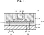
- FIG. 1 is a diagram illustrating a transistor 10 according to various example embodiments.
- the transistor 10 may be disposed on or in a substrate SUB.
- the transistor 10 may include an oxide semiconductor layer 110, a source electrode 120 and a drain electrode 130 disposed on the oxide semiconductor layer 110 and spaced apart from each other, a gate electrode 140 disposed to be spaced apart from the oxide semiconductor layer 110, and a gate insulating layer 150 disposed between the oxide semiconductor layer 110 and the gate electrode 140.
- the substrate SUB may be provided in a flat plate shape extending along one surface thereof.
- the substrate SUB may include a material for forming a device, and a material having good or excellent mechanical strength and/or dimensional stability may be selected.
- the material of the substrate SUB may include, but is not limited to, a glass plate, a metal plate, a ceramic plate, or plastic (a polycarbonate resin, a polyester resin, an epoxy resin, a silicone resin, a fluorine resin, etc.).
- a first interlayer insulating layer (e.g., a first interlayer dielectric (ILD1)) may be disposed on the substrate SUB.
- the oxide semiconductor layer 110 may be disposed on the first interlayer insulating layer ILD1.
- the oxide semiconductor layer 110 may be provided in the form of an ultra-thin film.
- a thickness of the oxide semiconductor layer 110 may be 30 nm or less.
- the oxide semiconductor layer 110 according to an example may include metal elements of group 12, 13 and 14 such as zinc (Zn), indium (In), gallium (Ga), tin (Sn), cadmium (Cd), germanium (Ge), or hafnium (Hf), and oxides of materials selected from one or combinations thereof.
- the oxide semiconductor layer 110 may be formed of a Zn oxide-based material, such as one or more of Zn oxide, In-Zn oxide, Ga-In-Zn oxide, or the like.
- the oxide semiconductor layer 110 may be provided as a single-layer or as a multi-layer structure.
- the source electrode 120 and the drain electrode 130 may be disposed on the oxide semiconductor layer 110 and spaced apart from each other.
- the source electrode 120 and the drain electrode 130 may be disposed on the same surface of the oxide semiconductor layer 110.
- the source electrode 120 and the drain electrode 130 may include an electrically conductive material.
- the source electrode 120 and the drain electrode 130 may include a metal and/or a metal compound, and may include the same, or different materials.
- the gate electrode 140 may be disposed between the source electrode 120 and the drain electrode 130 on the oxide semiconductor layer 110.
- the gate electrode 140, the source electrode 120, and the drain electrode 130 may be disposed on the same surface of the oxide semiconductor layer 110.
- the gate electrode 140 may include an electrically conductive material.
- the gate electrode 140 may include a metal and/or a metal compound.
- the transistor 10 includes a graphene layer 160 doped with, and/or having incorporated therein, a metal between the gate insulating layer 150 and the gate electrode 140.
- the metal may be interstitially within the graphene, and/or may be substitutional within the graphene; example embodiments are not limited thereto.
- the metal may be doped in an amount of about 0.2 at% or more, 0.5 at% or more, 2 at% or more, 3 at% or more, 4 at% or less, or 5 at% or less with respect to a total amount of the metal-doped graphene layer 160
- a thickness of the graphene layer 160 may be less than a thickness of the gate electrode 140.
- the thickness of the graphene layer 160 may be about 10 nm or less.
- the metal-doped graphene layer 160 may increase a work function to increase the threshold voltage of the transistor 10.
- An ideal threshold voltage V T of the transistor 10 may be expressed as in Equation 1 below.
- V T ⁇ ms ⁇ Q i C i ⁇ Q d C i + 2 ⁇ F
- Ci represents capacitance of the gate insulating layer 150
- Qi represents the amount of charges in the gate insulating layer 150
- Qd represents the amount of deflation charges in the gate insulating layer 150
- ⁇ f represents a Fermi level of the oxide semiconductor layer 110.
- the threshold voltage V T of the transistor 10 may increase when Ci is large, for example, when one or more of the gate insulating layer 150 is high-k, the thickness of the gate insulating layer 150 is small, or the work function of the gate electrode 140 is large.
- W or TiN may be used for the gate electrode 140.
- a work function of W or TiN may be about 4.3 to 4.65 eV.
- an undoped graphene layer may have a work function of about 4.65 eV, which is greater than that of a metal. If the graphene layer is doped with or has incorporated therein a metal, the grapheme layer may have a higher work function.
- a graphene layer doped with Ru has a work function of 4.9 to 5.1 eV, and thus may have a higher work function of about 0.5 eV than a gate electrode including a metal material.
- the metal-doped graphene layer 160 having a high work function when the metal-doped graphene layer 160 having a high work function is disposed between the gate insulating layer 150 and the gate electrode 140, the metal-doped graphene layer 160 may serve as the gate electrode 140, thereby increasing the threshold voltage of the transistor 10.
- the graphene layer 160 may prevent or reduce the amount of or impact from material diffusion between the layers.
- Hydrogen is a dopant of an oxide semiconductor, and when the content of hydrogen in the oxide semiconductor layer 110 increases, the threshold voltage of the oxide semiconductor layer 110 decreases.
- hydrogen may be introduced into the oxide semiconductor layer 110, and during high-temperature driving of the transistor 10, hydrogen may be introduced into the oxide semiconductor layer 110 due to bias stress.
- the introduced hydrogen lowers the threshold voltage of the oxide semiconductor layer 110. For example, in order to increase thermal stability and reliability of device driving, it is necessary or desirable to prevent or reduce hydrogen from diffusing into the oxide semiconductor layer 110.
- the carbon atoms of graphene may act as a diffusion barrier that effectively prevents or reduces material diffusion. Accordingly, by forming the graphene layer 160 on the gate insulating layer 150, hydrogen diffusing from the gate electrode 140 may be or at least partially be properly blocked, thereby improving the reliability of the threshold voltage control.
- the metal-doped graphene layer 160 may be in contact with two or more surfaces of the gate electrode 140.
- the metal-doped graphene layer 160 may be in contact with a lower surface and side surfaces of the gate electrode 140.
- the metal-doped graphene layer 160 may effectively prevent or reduce the material of the gate electrode 140 from diffusing to the outside.
- the gate insulating layer 150 may also cover two or more surfaces of the gate electrode 140.
- the gate insulating layer 150 may be disposed on the lower surface and side surfaces of the gate electrode 140.
- the gate insulating layer 150 may insulate the gate electrode 140 from the oxide semiconductor layer 110 as well as insulate the gate electrode 140, the source electrode 120, and the drain electrode 130. Thus, a length or a channel length of the oxide semiconductor layer 110 may be reduced.
- the source electrode 120 and the drain electrode 130 may include a stepped shape.
- the source electrode 120 may include a first source electrode 121 having a first thickness and a second source electrode 122 having a second thickness less than the first thickness, and the second source electrode 122 may be disposed closer to the gate electrode 140 than the first source electrode 121.
- the source electrode 120 having a stepped shape may reduce formation of parasitic capacitance between the gate electrode 140 and the source electrode 120, while securing or helping to secure a contact area with the oxide semiconductor layer 110.
- the drain electrode 130 may have a symmetrical structure with the source electrode 120 with respect to the gate electrode 140.
- the drain electrode 130 may include a first drain electrode 131 having a first thickness and a second drain electrode 132 having a second thickness less than the first thickness, and the second drain electrode 132 may be disposed closer to the gate electrode 140 than the first drain electrode 130.
- the drain electrode 130 having a stepped shape may reduce formation of a parasitic capacitance between the gate electrode 140 and the source electrode 120, while securing a contact area with the oxide semiconductor layer 110.
- the source electrode 120 and the drain electrode 130 may be in contact with even the gate insulating layer 150.
- the transistor 10 may be integrated, while reducing the length of the oxide semiconductor layer 110.
- a second interlayer insulating layer ILD2 may fill a gap between the gate insulating layer 150 and the source electrode 120 and between the gate insulating layer 150 and the drain electrode 130.
- the second interlayer insulating layer ILD2 may electrically disconnect the oxide semiconductor layer 110, the gate electrode 140, the source electrode 120, and the drain electrode 130 from each other.
- the second interlayer insulating layer ILD2 may be in contact with the first interlayer insulating layer ILD1, and bury the oxide semiconductor layer 110, the gate insulating layer 150, the gate electrode 140, the source electrode 120, and the drain electrode 130.
- FIG. 2 is results of measuring a work function of each material according to various example embodiments.
- a work function of a material including TiN and W was about 4.3 eV or more and 4.65 eV or less, and a work function of graphene was about 4.5 eV or more and 4.65 eV or less.
- a work function of the graphene layer doped with a metalloid (e.g., As) and a non-metal (e.g., P) was about 4.7 eV or more and 4.8 eV or less.
- a work function of a graphene layer doped with a metal, for example, Ru was about 4.9 eV or more and 5.1 eV or less.
- a graphene layer When a graphene layer is added to the gate electrode, it may be expected that the work function increases. In particular, when a metal-doped graphene layer is added to the gate electrode, it may be expected that a work function exceeds 4.8 eV.
- a work function of the metal-doped graphene layer according to various example embodiments may be 4.8 eV or more and 5.3 eV or less.
- a work function of the metal-doped graphene layer according to various example embodiments is 4.9 eV or more and 5.1 eV or less.
- the metal-doped graphene layer may be applied to various types of transistors.
- FIG. 4 is a diagram illustrating a transistor 10a having a top gate structure according to various example embodiments. Comparing FIG. 4 with FIG. 1 , a source electrode 120a and a drain electrode 130a of the transistor 10a of FIG. 4 disposed to be spaced apart from each other on an oxide semiconductor layer 110a.
- a gate insulating layer 150a, a metal-doped graphene layer 160a, and a gate electrode 140a may be sequentially stacked on the oxide semiconductor layer 110a.
- the metal-doped graphene layer 160a may be disposed only on a lower surface of the gate electrode 140a, and the source electrode 120a and the drain electrode 130a may be disposed to be spaced apart from the gate insulating layer 150a.
- a length (e.g., a channel length) of the oxide semiconductor layer 110a of the transistor 10a of FIG. 4 may be longer than that of the transistor 10 of FIG. 1 .
- a metal doped in the graphene layer 160a may be different from a metal included in the oxide semiconductor layer 110a.
- the metal doped into the graphene layer 160a may include at least one of ruthenium (Ru), aluminum (Al), titanium (Ti), thallium (TI), platinum (Pt), tantalum (Ta), rhodium (Rh), iridium (Ir), cobalt (Co), and tungsten (W), and the oxide semiconductor layer 110a may be an oxide including at least one of In, Zn, Sn, Ga, and Hf.
- FIG. 5 is a diagram illustrating a transistor 10b having a bottom gate structure according to various example embodiments.
- a source electrode 120b and a drain electrode 130b of the transistor 10b of FIG. 5 may be disposed to be spaced apart from each other on an upper surface of an oxide semiconductor layer 110b, and a gate electrode 140b may be disposed on a lower surface of the oxide semiconductor layer 110b.
- a gate insulating layer 150b may be disposed between the oxide semiconductor layer 110b and the gate electrode 140b.
- a metal-doped graphene layer 160b may be disposed between the gate insulating layer 150b and the gate electrode 140b.
- the metal-doped graphene layer 160b may also be disposed on a side surface of the gate electrode 140b, as well as between the gate insulating layer 150b and the gate electrode 140b. Characteristics of each component have been described above, and thus, a detailed description thereof is omitted.
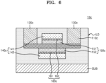
- FIG. 6 is a diagram illustrating a transistor 10c having a double gate structure according to various example embodiments.
- a gate insulating layer 150c may include a first gate insulating layer 151 disposed on an upper surface of an oxide semiconductor layer 110c and a second gate insulating layer 152 disposed on a lower surface of the oxide semiconductor layer 110.
- a gate electrode 140c may include a first gate electrode 141 disposed on an upper surface of the first gate insulating layer 151 and a second gate electrode 142 disposed on a lower surface of the second gate insulating layer 152.
- a graphene layer 160c may include a first graphene layer 161 disposed between the first gate insulating layer 151 and the first gate electrode 142 and a second graphene layer 162 disposed between the second gate insulating layer 152 and the second gate electrode 142.
- the first and second graphene layers 161 and 162 may be doped with a metal.
- the metal doped in the graphene layer 160c may be different from a metal included in the oxide semiconductor layer 110c.
- the metal doped in the graphene layer 160c may include at least one of ruthenium (Ru), aluminum (Al), titanium (Ti), thallium (Ti), platinum (Pt), tantalum (Ta), rhodium (Rh), iridium (Ir), cobalt (Co), and tungsten (W), and the oxide semiconductor layer 110c may be an oxide including at least one of In, Zn, Sn, Ga, and Hf.
- the metal may be doped in an amount of 0.2 at% or more, 0.5 at% or more, 2 at% or more, 3 at% or more, 4 at% or less, or 5 at% or less with respect to a total amount of the graphene layer 160c, and a thickness of the metal-doped graphene layer 160c is less than a thickness of the gate electrode 140c.
- the thickness of the graphene layer 160c may be about 10 nm or less.
- the source electrode and the drain electrode in contact with one surface of the oxide semiconductor layer have been described. However, various example embodiments are not limited thereto.
- the source electrode and the drain electrode may be in contact with a plurality of surfaces of the oxide semiconductor layer to integrate the transistor.
- FIG. 9 is a diagram illustrating a transistor 10f according to another embodiment.
- the transistor 10f may include a substrate SUB, an oxide semiconductor layer 110f disposed on the substrate SUB, a source electrode 120f in contact with three or more surfaces of the oxide semiconductor layer 110f, a drain region 130f in contact with three or more surfaces of the oxide semiconductor layer 110f, a gate electrode 140f apart from the oxide semiconductor layer, and a gate insulating layer 150f disposed between the oxide semiconductor layer 110f and the gate electrode 140f.
- the drain electrode 130f may also contact three or more surfaces of the oxide semiconductor layer 110f.
- the drain electrode 130f may include a second contact portion 133 in contact with the oxide semiconductor layer 110f and a second conductive plug 134 in contact with the second contact portion 133 and extending in one direction.
- the second contact portion 133 may be disposed between the oxide semiconductor layer 110f and the second conductive plug 134 and may contact the oxide semiconductor layer 110f on three or more surfaces.
- a thickness of an effective channel formed by a gate field may substantially be equal to the thickness of the physical oxide semiconductor layer 110f.
- a difference in charge concentration between a lower surface and an upper surface of the oxide semiconductor layer 110f is also reduced, so that a contact area in which the lower surface and the upper surface of the oxide semiconductor layer 110f are in contact with the drain electrode 130f and the drain region 130f may be formed.
- the second contact portion 133 may include a second lower contact layer 133-1 surrounding a portion of the lower surface of the oxide semiconductor layer 110f, a second upper contact layer 133-2 surrounding a portion of the upper surface of the oxide semiconductor layer 110f, and a second side contact layer 133-3 surrounding one side of the oxide semiconductor layer 110f.
- the second lower contact layer 133-1 may be disposed to face the substrate SUB.
- the second upper contact layer 133-2 may be disposed to face the second lower contact layer 133-1 with the oxide semiconductor layer 110f interposed therebetween.
- the second upper contact layer 133-2 may be provided to contact one end of the second conductive plug 134.
- the second side contact layer 133-3 may be disposed between the second lower contact layer 133-1 and the second upper contact layer 133-2 to connect the second lower contact layer 133-1 to the second upper contact layer 133-1.
- the transistor 10f includes a metal-doped graphene layer 160f between the gate electrode 140f and the gate insulating layer 150f.
- a metal doped in the graphene layer 160f may be different from a metal included in the oxide semiconductor layer 110f.
- the metal doped in the graphene layer 160f may include at least one of ruthenium (Ru), aluminum (Al), titanium (Ti), thallium (Ti), platinum (Pt), tantalum (Ta), rhodium (Rh), iridium (Ir), cobalt (Co), and tungsten (W), and the oxide semiconductor layer 110f may be an oxide including at least one of In, Zn, Sn, Ga, and Hf.
- the metal may be doped in an amount of 0.2 at% or more, 0.5 at% or more, 2 at% or more, 3 at% or more, 4 at% or less, or 5 at% or less with respect to a total amount of the graphene layer 160f, and a thickness of the doped graphene layer 160f is less than a thickness of the gate electrode 140f.
- the thickness of the graphene layer 160f may be about 10 nm or less.
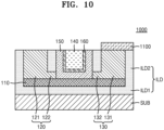
- FIG. 10 shows a memory device 1000 using the aforementioned transistor as a switching element and including a data storage element connected to the switching element.
- the transistor 100 of FIG. 1 among the transistors described above, may be used as a switching element.
- the memory device 1000 includes a data storage element 1100 on the interlayer insulating layer ILD.
- the data storage element 1100 may cover the entire upper surface of the drain electrode 130 and may be in direct contact with the upper surface.
- the data storage element 1100 may include a capacitor, a ferroelectric capacitor, and a magnetic tunnel junction (MTJ) cell.
- the memory device 1000 may be a volatile memory device, such as DRAM, or a nonvolatile memory device, such as FRAM, MRAM, ReRAM, or the like, depending on the data storage element 1100.
- FIG. 11 illustrates a memory device 2000 in which a plurality of memory cells MC1 of FIG. 10 are vertically stacked.
- a memory logic layer 2620 controlling an operation of the memory device 2000 is disposed on a substrate 2600, and a memory cell array 2640 is provided on the memory logic layer 2620.
- the memory cell array 2640 includes a plurality of vertically stacked memory cells MC1.
- the memory cell MC1 may be the memory device 1000 of FIG. 10 .
- the transistor including a metal-doped graphene layer has been illustrated and described, but various example embodiments are not limited to the specific exemplary embodiments described above, and may be variously modified by those skilled in the art to which the present invention pertains without departing from the scope of the present invention as claimed in the claims.
- a threshold voltage of a transistor may be increased by adding a graphene layer doped with a metal having a large work function.
- the metal-doped graphene layer may serve as a barrier to improve the reliability of driving of the transistor.
Landscapes
- Thin Film Transistor (AREA)
Description
- Various example embodiments relates to transistors including an oxide semiconductor layer.
- Oxide semiconductor devices including a transparent semiconductor material having a wide bandgap of 3.0 eV or greater have been studied for many years. The oxide semiconductor devices are mass-produced as driving devices for large-area OLED TVs.
- As the degree of device integration of semiconductor devices increases, the devices are required or desired to be smaller. In the case of a transistor, as a size thereof is reduced, a channel length may decrease. A decrease in the channel length of the transistor may cause or may exacerbate a short channel effect that results in a shift of a threshold voltage. Document
US10734378B2 - Provided are transistors having improved operation reliability.
- However, problems to be solved are not limited to the above disclosure. Additional aspects will be set forth in part in the description which follows and, in part, will be apparent from the description, and/or may be learned by practice of various example embodiments.
- According to a claimed embodiment, a transistor as defined by
claim 1 includes an oxide semiconductor layer; a source electrode and a drain electrode on the oxide semiconductor layer and spaced apart from each other; a gate electrode spaced apart from the oxide semiconductor layer; a gate insulating layer between the oxide semiconductor layer and the gate electrode; and a graphene layer between the gate electrode and the gate insulating layer and doped with a metal. - The metal doped in the graphene layer may be different from a metal included in the oxide semiconductor layer.
- The metal doped into the graphene layer may include at least one of ruthenium (Ru), aluminum (Al), titanium (Ti), thallium (TI), platinum (Pt), tantalum (Ta), rhodium (Rh), iridium (Ir), cobalt (Co), and tungsten (W).
- The metal may be doped in an amount of 0.2 at% or more and 5 at% or less with respect to a total amount of the graphene layer.
- A work function of the graphene layer may be 4.9 eV or more and 5.1 eV or less.
- A threshold voltage of the transistor may be a positive value when a current flowing from the drain electrode to the source electrode is 10-12A/micron.
- A thickness of the graphene layer may be less than a thickness of the gate electrode.
- The thickness of the graphene layer may be 10 nm or less.
- The oxide semiconductor layer may include at least one of In, Zn, Sn, Ga, and Hf.
- The graphene layer may be in contact with two or more surfaces of the gate electrode.
- The graphene layer may be in contact with a lower surface of the gate electrode and a side surface of the gate electrode.
- The gate insulating layer may at least partially cover two or more surfaces of the gate electrode.
- The gate insulating layer may at least partially cover a lower surface of the gate electrode and a side surface of the gate electrode.
- The gate insulating layer may be in contact with at least one of the source electrode and the drain electrode.
- At least one of the source electrode and the drain electrode may include a stepped shape.
- At least one of the source electrode and the drain electrode may include a first region having a first thickness and a second region having a second thickness less than the first thickness, wherein the second region may be closer to the gate electrode than the first region.
- The source electrode, the drain electrode, and the gate insulating layer may be on a same surface of the oxide semiconductor layer.
- The source electrode and the drain electrode may be on a first surface of the oxide semiconductor layer, and the gate insulating layer may be on a second surface, different from the first surface of the oxide semiconductor layer.
- The gate insulating layer may include a first gate insulating layer in contact with a first surface of the oxide semiconductor layer and a second gate insulating layer in contact with a second surface, different from the first surface of the oxide semiconductor layer. The gate electrode may include a first gate electrode on the first gate insulating layer and a second gate electrode on the second gate insulating layer. The graphene layer may include a first graphene layer between the first gate insulating layer and the first gate electrodes and a second graphene layer between the second gate insulating layer and the second gate electrode.
- The source electrode, the oxide semiconductor layer, and the drain electrode may be sequentially arranged in one direction.
- The gate insulating layer may entirely surround a side surface of the oxide semiconductor layer.
- The above and other aspects, features, and advantages of certain embodiments of the disclosure will be more apparent from the following description taken in conjunction with the accompanying drawings, in which:
-
FIG. 1 is a diagram illustrating a transistor according to various example embodiments; -
FIG. 2 shows results of measuring a work function of a material according to various example embodiments; -
FIG. 3 shows results of measuring IV characteristics of a transistor according to various example embodiments; -
FIG. 4 is a diagram illustrating a transistor having a top gate structure according to another embodiment; -
FIG. 5 is a diagram illustrating a transistor having a bottom gate structure according to various example embodiments; -
FIG. 6 is a diagram illustrating a transistor having a double gate structure according to various example embodiments; -
FIG. 7 is a diagram illustrating a transistor having a vertical channel structure according to various example embodiments; -
FIG. 8 is a diagram illustrating a transistor having a gate-all-around structure according to various example embodiments; -
FIG. 9 is a diagram illustrating a transistor according to another embodiment; -
FIG. 10 shows a memory device including the aforementioned transistor as a switching element and a data storage device connected to the switching element; and -
FIG. 11 illustrates a memory device in which a plurality of memory devices ofFIG. 10 are vertically stacked. - Reference will now be made in detail to various embodiments, examples of which are illustrated in the accompanying drawings, wherein like reference numerals refer to like elements throughout. In this regard, example embodiments may have different forms and should not be construed as being limited to the descriptions set forth herein. Accordingly, example embodiments are merely described below, by referring to the figures, to explain aspects. As used herein, the term "and/or" includes any and all combinations of one or more of the associated listed items. Expressions such as "at least one of," when preceding a list of elements, modify the entire list of elements and do not modify the individual elements of the list.
- Example embodiments are described in detail with reference to the accompanying drawings. In the following drawings, like reference numerals refer to like components, and the size of each component in the drawings may be exaggerated for clarity and convenience of description. The embodiments described herein are merely examples, and various modifications may be made from these embodiments.
- When it is described that a certain component is "above" or "on" another component, the certain component may be directly above another component, or a third component may be interposed therebetween. The singular expressions include plural expressions unless the context clearly dictates otherwise. When a part "includes" a component, it may indicate that the part does not exclude another component but may further include another component, unless otherwise stated. The use of the terms "a" and "an" and "the" and similar referents may cover both the singular and the plural.
-
FIG. 1 is a diagram illustrating atransistor 10 according to various example embodiments. Referring toFIG. 1 , thetransistor 10 may be disposed on or in a substrate SUB. Thetransistor 10 may include anoxide semiconductor layer 110, asource electrode 120 and adrain electrode 130 disposed on theoxide semiconductor layer 110 and spaced apart from each other, agate electrode 140 disposed to be spaced apart from theoxide semiconductor layer 110, and agate insulating layer 150 disposed between theoxide semiconductor layer 110 and thegate electrode 140. - The substrate SUB may be provided in a flat plate shape extending along one surface thereof. The substrate SUB may include a material for forming a device, and a material having good or excellent mechanical strength and/or dimensional stability may be selected. The material of the substrate SUB may include, but is not limited to, a glass plate, a metal plate, a ceramic plate, or plastic (a polycarbonate resin, a polyester resin, an epoxy resin, a silicone resin, a fluorine resin, etc.).
- A first interlayer insulating layer (e.g., a first interlayer dielectric (ILD1)) may be disposed on the substrate SUB. The
oxide semiconductor layer 110 may be disposed on the first interlayer insulating layer ILD1. As an example, theoxide semiconductor layer 110 may be provided in the form of an ultra-thin film. For example, a thickness of theoxide semiconductor layer 110 may be 30 nm or less. Theoxide semiconductor layer 110 according to an example may include metal elements of group 12, 13 and 14 such as zinc (Zn), indium (In), gallium (Ga), tin (Sn), cadmium (Cd), germanium (Ge), or hafnium (Hf), and oxides of materials selected from one or combinations thereof. For example, theoxide semiconductor layer 110 may be formed of a Zn oxide-based material, such as one or more of Zn oxide, In-Zn oxide, Ga-In-Zn oxide, or the like. As an example, theoxide semiconductor layer 110 may be provided as a single-layer or as a multi-layer structure. - The
source electrode 120 and thedrain electrode 130 may be disposed on theoxide semiconductor layer 110 and spaced apart from each other. Thesource electrode 120 and thedrain electrode 130 may be disposed on the same surface of theoxide semiconductor layer 110. Thesource electrode 120 and thedrain electrode 130 may include an electrically conductive material. For example, thesource electrode 120 and thedrain electrode 130 may include a metal and/or a metal compound, and may include the same, or different materials. - The
gate electrode 140 may be disposed between thesource electrode 120 and thedrain electrode 130 on theoxide semiconductor layer 110. Thegate electrode 140, thesource electrode 120, and thedrain electrode 130 may be disposed on the same surface of theoxide semiconductor layer 110. According to some example embodiments, thegate electrode 140 may include an electrically conductive material. For example, thegate electrode 140 may include a metal and/or a metal compound. - The
gate insulating layer 150 may be disposed between theoxide semiconductor layer 110 and thegate electrode 140 to electrically disconnect theoxide semiconductor layer 110 and thegate electrode 140. For example, thegate insulating layer 150 may include a ferroelectric material. As an example, the ferroelectric material may include at least one of an oxide ferroelectric material, a polymer ferroelectric material, a fluoride ferroelectric material such as BaMgF4 (BMF), and/or a ferroelectric material semiconductor. - The
transistor 10 including theoxide semiconductor layer 110 has a wide bandgap of 3.0 eV or greater. In addition, thetransistor 10 including theoxide semiconductor layer 110 may reduce an OFF-current, have a low subthreshold swing (SS), and/or have a high ON/OFF ratio. - When such a
transistor 10 is applied as a driving element of an electronic device, for example, a display device, a short-channel effect due to scaling down may exist or be pronounced, varying performance. Typically, a length of thetransistor 10 may be reduced, so it may be difficult to control a threshold voltage. In general, in the process of forming other components of thetransistor 10 after theoxide semiconductor layer 110 is formed, a conductivity of theoxide semiconductor layer 110 may increase due to the influence of a process such as plasma damage and/or an increase in the hydrogen (H) concentration. As a result, a threshold voltage of thetransistor 10 may be reduced. Alternatively or additionally, when hetransistor 10 is driven in a high temperature, high voltage state, the threshold voltage may be shifted to a negative value due to migration of hydrogen. - The
transistor 10 according to various example embodiments includes agraphene layer 160 doped with, and/or having incorporated therein, a metal between thegate insulating layer 150 and thegate electrode 140. The metal may be interstitially within the graphene, and/or may be substitutional within the graphene; example embodiments are not limited thereto. - The metal doped in the
graphene layer 160 may be different from a metal included in theoxide semiconductor layer 110. For example, the metal doped in thegraphene layer 160 may include at least one of ruthenium (Ru), aluminum (Al), titanium (Ti), thallium (TI), platinum (Pt), tantalum (Ta), rhodium (Rh), iridium (Ir), cobalt (Co), and tungsten (W). The metal may be doped in an amount of about 0.2 at% or more, 0.5 at% or more, 2 at% or more, 3 at% or more, 4 at% or less, or 5 at% or less with respect to a total amount of the metal-doped graphene layer 160 A thickness of thegraphene layer 160 may be less than a thickness of thegate electrode 140. The thickness of thegraphene layer 160 may be about 10 nm or less. - The metal-doped
graphene layer 160 may increase a work function to increase the threshold voltage of thetransistor 10. An ideal threshold voltage VT of thetransistor 10 may be expressed as inEquation 1 below.
- Here, Φms = Φm - Φs represents a difference between a work function Φm of the
gate electrode 140 and a work function Φs of theoxide semiconductor layer 110, Ci represents capacitance of thegate insulating layer 150, Qi represents the amount of charges in thegate insulating layer 150, Qd represents the amount of deflation charges in thegate insulating layer 150, and Φf represents a Fermi level of theoxide semiconductor layer 110. - According to
Equation 1, in general, the threshold voltage VT of thetransistor 10 may increase when Ci is large, for example, when one or more of thegate insulating layer 150 is high-k, the thickness of thegate insulating layer 150 is small, or the work function of thegate electrode 140 is large. - In general, W or TiN may be used for the
gate electrode 140. A work function of W or TiN may be about 4.3 to 4.65 eV. Meanwhile, an undoped graphene layer may have a work function of about 4.65 eV, which is greater than that of a metal. If the graphene layer is doped with or has incorporated therein a metal, the grapheme layer may have a higher work function. For example, a graphene layer doped with Ru has a work function of 4.9 to 5.1 eV, and thus may have a higher work function of about 0.5 eV than a gate electrode including a metal material. Therefore, when the metal-dopedgraphene layer 160 having a high work function is disposed between thegate insulating layer 150 and thegate electrode 140, the metal-dopedgraphene layer 160 may serve as thegate electrode 140, thereby increasing the threshold voltage of thetransistor 10. - Alternatively or additionally, the
graphene layer 160 may prevent or reduce the amount of or impact from material diffusion between the layers. Hydrogen is a dopant of an oxide semiconductor, and when the content of hydrogen in theoxide semiconductor layer 110 increases, the threshold voltage of theoxide semiconductor layer 110 decreases. During a thin film deposition and/or a heat treatment process of thetransistor 10, hydrogen may be introduced into theoxide semiconductor layer 110, and during high-temperature driving of thetransistor 10, hydrogen may be introduced into theoxide semiconductor layer 110 due to bias stress. The introduced hydrogen lowers the threshold voltage of theoxide semiconductor layer 110. For example, in order to increase thermal stability and reliability of device driving, it is necessary or desirable to prevent or reduce hydrogen from diffusing into theoxide semiconductor layer 110. Because carbon atoms of graphene have a small bonding length and are bound by strong covalent bonds, the carbon atoms may act as a diffusion barrier that effectively prevents or reduces material diffusion. Accordingly, by forming thegraphene layer 160 on thegate insulating layer 150, hydrogen diffusing from thegate electrode 140 may be or at least partially be properly blocked, thereby improving the reliability of the threshold voltage control. - For example, the metal-doped
transistor 10 according to various example embodiments has a large work function, so that the metal-dopedtransistor 10 may serve as a barrier to prevent or reduce material diffusion, while serving as thegate electrode 140, thereby improving the reliability of driving of the transistor. - The metal-doped
graphene layer 160 may be in contact with two or more surfaces of thegate electrode 140. For example, the metal-dopedgraphene layer 160 may be in contact with a lower surface and side surfaces of thegate electrode 140. The metal-dopedgraphene layer 160 may effectively prevent or reduce the material of thegate electrode 140 from diffusing to the outside. - The
gate insulating layer 150 may also cover two or more surfaces of thegate electrode 140. For example, thegate insulating layer 150 may be disposed on the lower surface and side surfaces of thegate electrode 140. Thegate insulating layer 150 may insulate thegate electrode 140 from theoxide semiconductor layer 110 as well as insulate thegate electrode 140, thesource electrode 120, and thedrain electrode 130. Thus, a length or a channel length of theoxide semiconductor layer 110 may be reduced. - The
source electrode 120 and thedrain electrode 130 may include a stepped shape. For example, thesource electrode 120 may include afirst source electrode 121 having a first thickness and asecond source electrode 122 having a second thickness less than the first thickness, and thesecond source electrode 122 may be disposed closer to thegate electrode 140 than thefirst source electrode 121. The source electrode 120 having a stepped shape may reduce formation of parasitic capacitance between thegate electrode 140 and thesource electrode 120, while securing or helping to secure a contact area with theoxide semiconductor layer 110. - The
drain electrode 130 may have a symmetrical structure with thesource electrode 120 with respect to thegate electrode 140. For example, thedrain electrode 130 may include afirst drain electrode 131 having a first thickness and asecond drain electrode 132 having a second thickness less than the first thickness, and thesecond drain electrode 132 may be disposed closer to thegate electrode 140 than thefirst drain electrode 130. Thedrain electrode 130 having a stepped shape may reduce formation of a parasitic capacitance between thegate electrode 140 and thesource electrode 120, while securing a contact area with theoxide semiconductor layer 110. - Alternatively or additionally, at least one of the
source electrode 120 and thedrain electrode 130 may be in contact with even thegate insulating layer 150. Thus, thetransistor 10 may be integrated, while reducing the length of theoxide semiconductor layer 110. - A second interlayer insulating layer ILD2 may fill a gap between the
gate insulating layer 150 and thesource electrode 120 and between thegate insulating layer 150 and thedrain electrode 130. The second interlayer insulating layer ILD2 may electrically disconnect theoxide semiconductor layer 110, thegate electrode 140, thesource electrode 120, and thedrain electrode 130 from each other. As an example, the second interlayer insulating layer ILD2 may be in contact with the first interlayer insulating layer ILD1, and bury theoxide semiconductor layer 110, thegate insulating layer 150, thegate electrode 140, thesource electrode 120, and thedrain electrode 130. -
FIG. 2 is results of measuring a work function of each material according to various example embodiments. Referring toFIG. 2 , a work function of a material including TiN and Wwas about 4.3 eV or more and 4.65 eV or less, and a work function of graphene was about 4.5 eV or more and 4.65 eV or less. A work function of the graphene layer doped with a metalloid (e.g., As) and a non-metal (e.g., P) was about 4.7 eV or more and 4.8 eV or less. A work function of a graphene layer doped with a metal, for example, Ru, was about 4.9 eV or more and 5.1 eV or less. - When a graphene layer is added to the gate electrode, it may be expected that the work function increases. In particular, when a metal-doped graphene layer is added to the gate electrode, it may be expected that a work function exceeds 4.8 eV. A work function of the metal-doped graphene layer according to various example embodiments may be 4.8 eV or more and 5.3 eV or less. Alternatively, a work function of the metal-doped graphene layer according to various example embodiments is 4.9 eV or more and 5.1 eV or less.
-
FIG. 3 is results of measuring current-voltage (IV) characteristics of thetransistor 10 according to various example embodiments. Example is IV characteristics of a transistor including a metal-doped graphene layer, and Comparative Example is IV characteristics of a transistor not including a metal-doped graphene layer. It can be seen that, when a current IDS flowing from thedrain electrode 130 to thesource electrode 120 is 10-12 A/µm or 10-12 A/micron, a threshold voltage of Example is a positive voltage, whereas a threshold voltage of Comparative Example is a negative voltage. Therefore, it can be seen that the threshold voltage may be maintained at a positive value even when the drain current is 10-12 A/µm by adding the metal-dopedgraphene layer 160 to thegate electrode 140. - The metal-doped graphene layer may be applied to various types of transistors.
-
FIG. 4 is a diagram illustrating atransistor 10a having a top gate structure according to various example embodiments. ComparingFIG. 4 withFIG. 1 , asource electrode 120a and adrain electrode 130a of thetransistor 10a ofFIG. 4 disposed to be spaced apart from each other on anoxide semiconductor layer 110a. In addition, agate insulating layer 150a, a metal-dopedgraphene layer 160a, and agate electrode 140a may be sequentially stacked on theoxide semiconductor layer 110a. The metal-dopedgraphene layer 160a may be disposed only on a lower surface of thegate electrode 140a, and thesource electrode 120a and thedrain electrode 130a may be disposed to be spaced apart from thegate insulating layer 150a. A length (e.g., a channel length) of theoxide semiconductor layer 110a of thetransistor 10a ofFIG. 4 may be longer than that of thetransistor 10 ofFIG. 1 . - A metal doped in the
graphene layer 160a may be different from a metal included in theoxide semiconductor layer 110a. For example, the metal doped into thegraphene layer 160a may include at least one of ruthenium (Ru), aluminum (Al), titanium (Ti), thallium (TI), platinum (Pt), tantalum (Ta), rhodium (Rh), iridium (Ir), cobalt (Co), and tungsten (W), and theoxide semiconductor layer 110a may be an oxide including at least one of In, Zn, Sn, Ga, and Hf. The metal may be doped in an amount of 0.2 at% or more, 0.5 at% or more, 2 at% or more, 3 at% or more, 4 at% or less, or 5 at% or less with respect to a total amount of thegraphene layer 160a, and a thickness of the dopedgraphene layer 160a is less than a thickness of thegate electrode 140a. For example, the thickness of thegraphene layer 160a may be about 10 nm or less. -
FIG. 5 is a diagram illustrating atransistor 10b having a bottom gate structure according to various example embodiments. ComparingFIG. 5 withFIG. 2 , asource electrode 120b and adrain electrode 130b of thetransistor 10b ofFIG. 5 may be disposed to be spaced apart from each other on an upper surface of anoxide semiconductor layer 110b, and agate electrode 140b may be disposed on a lower surface of theoxide semiconductor layer 110b. Agate insulating layer 150b may be disposed between theoxide semiconductor layer 110b and thegate electrode 140b. A metal-dopedgraphene layer 160b may be disposed between thegate insulating layer 150b and thegate electrode 140b. The metal-dopedgraphene layer 160b may also be disposed on a side surface of thegate electrode 140b, as well as between thegate insulating layer 150b and thegate electrode 140b. Characteristics of each component have been described above, and thus, a detailed description thereof is omitted. -
FIG. 6 is a diagram illustrating atransistor 10c having a double gate structure according to various example embodiments. ComparingFIG. 6 withFIG. 2 , a gate insulating layer 150c may include a firstgate insulating layer 151 disposed on an upper surface of anoxide semiconductor layer 110c and a second gate insulating layer 152 disposed on a lower surface of theoxide semiconductor layer 110. Agate electrode 140c may include a first gate electrode 141 disposed on an upper surface of the firstgate insulating layer 151 and a second gate electrode 142 disposed on a lower surface of the second gate insulating layer 152. In addition, agraphene layer 160c may include afirst graphene layer 161 disposed between the firstgate insulating layer 151 and the first gate electrode 142 and asecond graphene layer 162 disposed between the second gate insulating layer 152 and the second gate electrode 142. The first and second graphene layers 161 and 162 may be doped with a metal. - The metal doped in the
graphene layer 160c may be different from a metal included in theoxide semiconductor layer 110c. For example, the metal doped in thegraphene layer 160c may include at least one of ruthenium (Ru), aluminum (Al), titanium (Ti), thallium (Ti), platinum (Pt), tantalum (Ta), rhodium (Rh), iridium (Ir), cobalt (Co), and tungsten (W), and theoxide semiconductor layer 110c may be an oxide including at least one of In, Zn, Sn, Ga, and Hf. The metal may be doped in an amount of 0.2 at% or more, 0.5 at% or more, 2 at% or more, 3 at% or more, 4 at% or less, or 5 at% or less with respect to a total amount of thegraphene layer 160c, and a thickness of the metal-dopedgraphene layer 160c is less than a thickness of thegate electrode 140c. For example, the thickness of thegraphene layer 160c may be about 10 nm or less. -
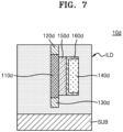
FIG. 7 is a diagram illustrating atransistor 10d having a vertical channel structure according to various example embodiments. Referring toFIG. 7 , anoxide semiconductor layer 110d may have a structure extending in a thickness direction of the substrate SUB. Asource electrode 120d may be disposed on an upper surface of theoxide semiconductor layer 110d, and adrain electrode 130d may be disposed on a lower surface of theoxide semiconductor layer 110d. However, various example embodiments are not limited thereto. Thedrain electrode 130d may be disposed on the upper surface of theoxide semiconductor layer 110d and thesource electrode 120d may be disposed on the lower surface of theoxide semiconductor layer 110d. Agate insulating layer 150d and agate electrode 140d may be disposed on a side surface of theoxide semiconductor layer 110d. In addition, the metal-dopedgraphene layer 160d may be disposed between thegate insulating layer 150d and thegate electrode 140d. The metal-dopedgraphene layer 160d may cover two or more surfaces of thegate electrode 140. -
FIG. 8 is a diagram illustrating atransistor 10e having a gate-all-around structure according to various example embodiments. Referring toFIG. 8 , anoxide semiconductor layer 110e may have a structure extending in a thickness direction of the substrate SUB. Asource electrode 120e may be disposed on an upper surface of theoxide semiconductor layer 110e and adrain electrode 130e may be disposed on a lower surface of theoxide semiconductor layer 110e. However, various example embodiments are not limited thereto. Thedrain electrode 130e may be disposed on an upper surface of theoxide semiconductor layer 110e and thedrain electrode 130e may be disposed on a lower surface of theoxide semiconductor layer 110e. - A
gate insulating layer 150e covering the entire side surface of theoxide semiconductor layer 110e and agate electrode 140e covering the side surface of thegate insulating layer 150 may be further disposed. Also, the metal-dopedgraphene layer 160e may be disposed between thegate insulating layer 150e and thegate electrode 140e. The metal-dopedgraphene layer 160e may be disposed not only on the side surface of thegate electrode 140e but also on the upper and lower surfaces of thegate electrode 140e. - So far, the source electrode and the drain electrode in contact with one surface of the oxide semiconductor layer have been described. However, various example embodiments are not limited thereto. The source electrode and the drain electrode may be in contact with a plurality of surfaces of the oxide semiconductor layer to integrate the transistor.
-
FIG. 9 is a diagram illustrating atransistor 10f according to another embodiment. Referring toFIG. 9 , thetransistor 10f according to an example may include a substrate SUB, anoxide semiconductor layer 110f disposed on the substrate SUB, asource electrode 120f in contact with three or more surfaces of theoxide semiconductor layer 110f, adrain region 130f in contact with three or more surfaces of theoxide semiconductor layer 110f, agate electrode 140f apart from the oxide semiconductor layer, and agate insulating layer 150f disposed between theoxide semiconductor layer 110f and thegate electrode 140f. - The
source electrode 120f may be disposed to contact three or more surfaces of theoxide semiconductor layer 110f. As an example, thesource electrode 120f may include afirst contact portion 123 in contact with theoxide semiconductor layer 110f and a firstconductive plug 124 in contact with thefirst contact portion 123 and extending in one direction. - The
first contact portion 123 may be disposed between theoxide semiconductor layer 110f and the firstconductive plug 124 and may be in contact with theoxide semiconductor layer 110f on three or more surfaces. As described above, as a thickness h of theoxide semiconductor layer 110f decreases to an ultra-thin film, a thickness of an effective channel formed by a gate field may substantially be equal to a thickness of the physicaloxide semiconductor layer 110f. A difference in charge concentration between a lower surface and an upper surface of theoxide semiconductor layer 110f is also reduced, so that a contact area in which the entire area of theoxide semiconductor layer 110f is in contact with thesource electrode 120f and thedrain region 130f may be formed. - As an example, when the
oxide semiconductor layer 110f is provided in the form of a thin film extending along one plane, thefirst contact portion 123 may include a first lower contact layer 123-1 surrounding a portion of the lower surface of theoxide semiconductor layer 110f, a first upper contact layer 123-2 surrounding a portion of the upper surface of theoxide semiconductor layer 110f, and a first side contact layer 123-3 surrounding one side surface of theoxide semiconductor layer 110f. The first lower contact layer 123-1 may be disposed to face the substrate SUB. The first upper contact layer 123-2 may be disposed to face the first lower contact layer 123-1 with theoxide semiconductor layer 110f interposed therebetween. As an example, the first upper contact layer 123-2 may be provided to contact one end of the firstconductive plug 124. The first side contact layer 123-3 may be disposed between the first lower contact layer 123-1 and the first upper contact layer 123-2 to connect the first lower contact layer 123-1 to the first upper contact layer 123-2. - Like the
source electrode 120f, thedrain electrode 130f may also contact three or more surfaces of theoxide semiconductor layer 110f. As an example, thedrain electrode 130f may include asecond contact portion 133 in contact with theoxide semiconductor layer 110f and a secondconductive plug 134 in contact with thesecond contact portion 133 and extending in one direction. - The
second contact portion 133 may be disposed between theoxide semiconductor layer 110f and the secondconductive plug 134 and may contact theoxide semiconductor layer 110f on three or more surfaces. As described above, as the thickness of theoxide semiconductor layer 110f decreases to an ultra-thin film, a thickness of an effective channel formed by a gate field may substantially be equal to the thickness of the physicaloxide semiconductor layer 110f. A difference in charge concentration between a lower surface and an upper surface of theoxide semiconductor layer 110f is also reduced, so that a contact area in which the lower surface and the upper surface of theoxide semiconductor layer 110f are in contact with thedrain electrode 130f and thedrain region 130f may be formed. - As an example, when the
oxide semiconductor layer 110f is provided in the form of a thin film extending along one plane, thesecond contact portion 133 may include a second lower contact layer 133-1 surrounding a portion of the lower surface of theoxide semiconductor layer 110f, a second upper contact layer 133-2 surrounding a portion of the upper surface of theoxide semiconductor layer 110f, and a second side contact layer 133-3 surrounding one side of theoxide semiconductor layer 110f. The second lower contact layer 133-1 may be disposed to face the substrate SUB. The second upper contact layer 133-2 may be disposed to face the second lower contact layer 133-1 with theoxide semiconductor layer 110f interposed therebetween. As an example, the second upper contact layer 133-2 may be provided to contact one end of the secondconductive plug 134. The second side contact layer 133-3 may be disposed between the second lower contact layer 133-1 and the second upper contact layer 133-2 to connect the second lower contact layer 133-1 to the second upper contact layer 133-1. - The
transistor 10f includes a metal-dopedgraphene layer 160f between thegate electrode 140f and thegate insulating layer 150f. - A metal doped in the
graphene layer 160f may be different from a metal included in theoxide semiconductor layer 110f. For example, the metal doped in thegraphene layer 160f may include at least one of ruthenium (Ru), aluminum (Al), titanium (Ti), thallium (Ti), platinum (Pt), tantalum (Ta), rhodium (Rh), iridium (Ir), cobalt (Co), and tungsten (W), and theoxide semiconductor layer 110f may be an oxide including at least one of In, Zn, Sn, Ga, and Hf. The metal may be doped in an amount of 0.2 at% or more, 0.5 at% or more, 2 at% or more, 3 at% or more, 4 at% or less, or 5 at% or less with respect to a total amount of thegraphene layer 160f, and a thickness of the dopedgraphene layer 160f is less than a thickness of thegate electrode 140f. For example, the thickness of thegraphene layer 160f may be about 10 nm or less. -
FIG. 10 shows amemory device 1000 using the aforementioned transistor as a switching element and including a data storage element connected to the switching element. In an example, the transistor 100 ofFIG. 1 , among the transistors described above, may be used as a switching element. - Referring to
FIG. 10 , thememory device 1000 includes adata storage element 1100 on the interlayer insulating layer ILD. Thedata storage element 1100 may cover the entire upper surface of thedrain electrode 130 and may be in direct contact with the upper surface. Thedata storage element 1100 may include a capacitor, a ferroelectric capacitor, and a magnetic tunnel junction (MTJ) cell. Thememory device 1000 may be a volatile memory device, such as DRAM, or a nonvolatile memory device, such as FRAM, MRAM, ReRAM, or the like, depending on thedata storage element 1100. -
FIG. 11 illustrates amemory device 2000 in which a plurality of memory cells MC1 ofFIG. 10 are vertically stacked. - Referring to
FIG. 11 , amemory logic layer 2620 controlling an operation of thememory device 2000 is disposed on asubstrate 2600, and amemory cell array 2640 is provided on thememory logic layer 2620. Thememory cell array 2640 includes a plurality of vertically stacked memory cells MC1. In an example, the memory cell MC1 may be thememory device 1000 ofFIG. 10 . - In the above, the transistor including a metal-doped graphene layer has been illustrated and described, but various example embodiments are not limited to the specific exemplary embodiments described above, and may be variously modified by those skilled in the art to which the present invention pertains without departing from the scope of the present invention as claimed in the claims.
- According to various example embodiments, a threshold voltage of a transistor may be increased by adding a graphene layer doped with a metal having a large work function.
- The metal-doped graphene layer may serve as a barrier to improve the reliability of driving of the transistor.
- However, the effect of various example embodiments are not limited to the above disclosure.
- It should be understood that various example embodiments described herein should be considered in a descriptive sense only and not for purposes of limitation. Descriptions of features or aspects within each embodiment should typically be considered as available for other similar features or aspects in other example embodiments, and embodiments are not necessarily mutually exclusive. While one or more embodiments have been described with reference to the figures, it will be understood by those of ordinary skill in the art that various changes in form and details may be made therein without departing from the scope as defined by the following claims.
Claims (15)
- A transistor comprising:an oxide semiconductor (110) layer;a source electrode (120) and a drain electrode (130) spaced apart from each other on the oxide semiconductor layer;a gate electrode (140) spaced apart from the oxide semiconductor layer;a gate insulating layer (150) between the oxide semiconductor layer and the gate electrode; andcharacterised by a graphene layer (160) between the gate electrode and the gate insulating layer and doped with a metal.
- The transistor of claim 1, wherein the metal doped in the graphene layer is different from a metal included in the oxide semiconductor layer.
- The transistor of claim 1 or 2, wherein the metal doped into the graphene layer includes at least one of ruthenium (Ru), aluminum (Al), titanium (Ti), platinum (Pt), thallium (TI), tantalum (Ta), rhodium (Rh), iridium (Ir), cobalt (Co), and tungsten (W).
- The transistor of claim 1, 2 or 3, wherein the metal is doped into the graphene layer in an amount of 0.2 at% or more and 5 at% or less with respect to a total amount of the graphene layer.
- The transistor of any preceding claim, wherein a work function of the graphene layer is greater or equal to 4.9 eV or and less than or equal to 5.1 eV.
- The transistor of any preceding claim, wherein a threshold voltage of the transistor is positive when a current flowing from the drain electrode to the source electrode is 10-12A/micron.
- The transistor of any preceding claim, wherein a thickness of the graphene layer is less than a thickness of the gate electrode.
- The transistor of any preceding claim, wherein a thickness of the graphene layer is less than or equal to 10 nm.
- The transistor of any preceding claim, wherein the graphene layer is in contact with two or more surfaces of the gate electrode, and optionally wherein the graphene layer is in contact with a lower surface of the gate electrode and a side surface of the gate electrode.
- The transistor of any preceding claim, wherein the gate insulating layer at least partially covers two or more surfaces of the gate electrode.
- The transistor of any preceding claim, wherein the gate insulating layer at least partially covers a lower surface of the gate electrode and a side surface of the gate electrode.
- The transistor of any preceding claim, wherein at least one of the source electrode and the drain electrode includes a first region having a first thickness and a second region having a second thickness less than the first thickness, and the second region is closer to the gate electrode than the first region.
- The transistor of any preceding claim, wherein the source electrode and the drain electrode are on a first surface of the oxide semiconductor layer, and the gate insulating layer is on a second surface, different from the first surface of the oxide semiconductor layer.
- The transistor of any preceding claim, whereinthe gate insulating layer includes a first gate insulating layer in contact with a first surface of the oxide semiconductor layer and a second gate insulating layer in contact with a second surface different from the first surface of the oxide semiconductor layer,the gate electrode includes a first gate electrode on the first gate insulating layer and a second gate electrode on the second gate insulating layer, andthe graphene layer includes a first graphene layer between the first gate insulating layer and the first gate electrodes and a second graphene layer disposed between the second gate insulating layer and the second gate electrode.
- The transistor of any preceding claim, wherein the gate insulating layer entirely surrounds a side surface of the oxide semiconductor layer.
Applications Claiming Priority (1)
| Application Number | Priority Date | Filing Date | Title |
|---|---|---|---|
| KR1020220012580A KR20230115746A (en) | 2022-01-27 | 2022-01-27 | Transistor |
Publications (3)
| Publication Number | Publication Date |
|---|---|
| EP4220736A2 EP4220736A2 (en) | 2023-08-02 |
| EP4220736A3 EP4220736A3 (en) | 2023-08-09 |
| EP4220736B1 true EP4220736B1 (en) | 2025-05-07 |
Family
ID=85076238
Family Applications (1)
| Application Number | Title | Priority Date | Filing Date |
|---|---|---|---|
| EP23153062.7A Active EP4220736B1 (en) | 2022-01-27 | 2023-01-24 | Transistor |
Country Status (4)
| Country | Link |
|---|---|
| US (1) | US12575136B2 (en) |
| EP (1) | EP4220736B1 (en) |
| KR (1) | KR20230115746A (en) |
| CN (1) | CN116504843A (en) |
Families Citing this family (4)
| Publication number | Priority date | Publication date | Assignee | Title |
|---|---|---|---|---|
| KR20230115746A (en) * | 2022-01-27 | 2023-08-03 | 삼성전자주식회사 | Transistor |
| US12610552B2 (en) * | 2022-05-09 | 2026-04-21 | Taiwan Semiconductor Manufacturing Company, Ltd. | Memory device and method for forming the same |
| JP2024001809A (en) * | 2022-06-22 | 2024-01-10 | キオクシア株式会社 | Semiconductor devices and semiconductor storage devices |
| WO2025048406A1 (en) | 2023-08-31 | 2025-03-06 | 주식회사 엘지에너지솔루션 | Secondary battery electrolyte additive, lithium secondary battery non-aqueous electrolyte comprising same, and lithium secondary battery |
Family Cites Families (33)
| Publication number | Priority date | Publication date | Assignee | Title |
|---|---|---|---|---|
| US7732859B2 (en) * | 2007-07-16 | 2010-06-08 | International Business Machines Corporation | Graphene-based transistor |
| US8796668B2 (en) * | 2009-11-09 | 2014-08-05 | International Business Machines Corporation | Metal-free integrated circuits comprising graphene and carbon nanotubes |
| KR101823861B1 (en) | 2009-11-20 | 2018-01-31 | 가부시키가이샤 한도오따이 에네루기 켄큐쇼 | Nonvolatile latch circuit and logic circuit, and semiconductor device using the same |
| KR101803254B1 (en) | 2009-11-27 | 2017-11-30 | 가부시키가이샤 한도오따이 에네루기 켄큐쇼 | Semiconductor device |
| TWI539453B (en) | 2010-09-14 | 2016-06-21 | 半導體能源研究所股份有限公司 | Memory device and semiconductor device |
| KR101200237B1 (en) | 2010-12-06 | 2012-11-09 | 한양대학교 에리카산학협력단 | Thin Film Transistor for Display and Method of forming the same |
| WO2012090973A1 (en) | 2010-12-28 | 2012-07-05 | Semiconductor Energy Laboratory Co., Ltd. | Semiconductor device and manufacturing method thereof |
| US9177872B2 (en) | 2011-09-16 | 2015-11-03 | Micron Technology, Inc. | Memory cells, semiconductor devices, systems including such cells, and methods of fabrication |
| KR102059131B1 (en) * | 2013-04-05 | 2019-12-24 | 삼성전자주식회사 | Graphene device, and method of fabricating the same |
| KR102528615B1 (en) | 2014-03-13 | 2023-05-08 | 가부시키가이샤 한도오따이 에네루기 켄큐쇼 | Imaging device |
| US9812604B2 (en) | 2014-05-30 | 2017-11-07 | Klaus Y. J. Hsu | Photosensing device with graphene |
| JP6570417B2 (en) | 2014-10-24 | 2019-09-04 | 株式会社半導体エネルギー研究所 | Imaging apparatus and electronic apparatus |
| US10522693B2 (en) | 2015-01-16 | 2019-12-31 | Semiconductor Energy Laboratory Co., Ltd. | Memory device and electronic device |
| CN106409847B (en) | 2015-07-29 | 2020-05-12 | 联华电子股份有限公司 | Image Sensor Pixel Structure |
| US20170057827A1 (en) * | 2015-09-02 | 2017-03-02 | U.S.A. As Represented By The Administrator Of The National Aeronautics And Space Administration | Graphene transparent conductive electrode |
| US9564217B1 (en) | 2015-10-19 | 2017-02-07 | United Microelectronics Corp. | Semiconductor memory device having integrated DOSRAM and NOSRAM |
| KR102425131B1 (en) * | 2016-02-05 | 2022-07-26 | 광주과학기술원 | Graphene Transistor and Ternary Logic Device using the same |
| US10734378B2 (en) | 2016-04-01 | 2020-08-04 | Intel Corporation | Transistor threshold voltage variation optimization |
| US9647120B1 (en) * | 2016-10-19 | 2017-05-09 | International Business Machines Corporation | Vertical FET symmetric and asymmetric source/drain formation |
| CN110521003B (en) | 2017-03-27 | 2023-06-09 | 夏普株式会社 | Active matrix substrate and manufacturing method thereof |
| US11245038B2 (en) | 2017-03-30 | 2022-02-08 | Intel Corporation | Vertical multi-gate thin film transistors |
| CN107579003B (en) | 2017-08-31 | 2023-10-31 | 京东方科技集团股份有限公司 | Thin film transistor and manufacturing method, display substrate and manufacturing method, display device |
| KR102436715B1 (en) | 2017-11-10 | 2022-08-25 | 엘지디스플레이 주식회사 | Thin film trnasistor having doping portion for blocking hydrogen, method for manufacturing the same and display device comprising the same |
| KR102709935B1 (en) | 2018-06-29 | 2024-09-24 | 삼성전자주식회사 | Self-healing composite and device including the self-healing film |
| US20200091156A1 (en) | 2018-09-17 | 2020-03-19 | Intel Corporation | Two transistor memory cell using stacked thin-film transistors |
| KR102637107B1 (en) * | 2018-09-18 | 2024-02-15 | 삼성전자주식회사 | Electronic device and method of manufacturing the same |
| KR102669149B1 (en) | 2019-01-10 | 2024-05-24 | 삼성전자주식회사 | Semiconductor devices |
| US11017843B2 (en) | 2019-06-28 | 2021-05-25 | Intel Corporation | Thin film transistors for memory cell array layer selection |
| KR102906608B1 (en) | 2020-05-19 | 2025-12-30 | 삼성전자주식회사 | Oxide semiconductor transistor |
| KR20230115746A (en) * | 2022-01-27 | 2023-08-03 | 삼성전자주식회사 | Transistor |
| KR20240006969A (en) * | 2022-07-07 | 2024-01-16 | 삼성전자주식회사 | Semicondoctor device including graphene |
| KR20240032551A (en) * | 2022-09-02 | 2024-03-12 | 삼성전자주식회사 | Vertical transistor and manufacturing method |
| KR20240107972A (en) * | 2022-12-30 | 2024-07-09 | 삼성전자주식회사 | Semiconductor device including oxide material layer |
-
2022
- 2022-01-27 KR KR1020220012580A patent/KR20230115746A/en active Pending
-
2023
- 2023-01-23 US US18/158,176 patent/US12575136B2/en active Active
- 2023-01-24 EP EP23153062.7A patent/EP4220736B1/en active Active
- 2023-01-28 CN CN202310100911.0A patent/CN116504843A/en active Pending
Also Published As
| Publication number | Publication date |
|---|---|
| US12575136B2 (en) | 2026-03-10 |
| KR20230115746A (en) | 2023-08-03 |
| EP4220736A2 (en) | 2023-08-02 |
| US20230238460A1 (en) | 2023-07-27 |
| EP4220736A3 (en) | 2023-08-09 |
| CN116504843A (en) | 2023-07-28 |
Similar Documents
| Publication | Publication Date | Title |
|---|---|---|
| EP4220736A2 (en) | Transistor | |
| US12477745B2 (en) | Memory cell including spontaneously polarizable capacitor structure | |
| US12255244B2 (en) | Field effect transistor including gate insulating layer formed of two-dimensional material | |
| JP7307781B2 (en) | semiconductor equipment | |
| KR102715042B1 (en) | Capacitor and electronic device including the semiconductor device | |
| US8815695B2 (en) | Methods to improve leakage for ZrO2 based high K MIM capacitor | |
| US20180374929A1 (en) | Ferroelectric memory devices | |
| US8513773B2 (en) | Capacitor and semiconductor device including dielectric and N-type semiconductor | |
| TWI758052B (en) | semiconductor device | |
| US12183825B2 (en) | Thin film transistor including a hydrogen-blocking dielectric barrier and methods for forming the same | |
| US12160995B2 (en) | Wakeup free approach to improve the ferroelectricity of FeRAM using a stressor layer | |
| US20250344400A1 (en) | Anti-ferroelectric tunnel junction with asymmetrical metal electrodes | |
| US20250194147A1 (en) | Transistor, semiconductor memory device, and manufacturing method for transistor | |
| TWI830322B (en) | Semiconductor devices and semiconductor memory devices | |
| US12432971B2 (en) | Transistor including a hydrogen-diffusion barrier and methods for forming the same | |
| EP4345082A1 (en) | Capacitor comprising a vanadium oxide-based electrode and electronic device comprising it | |
| US10446689B1 (en) | Manufacturing method of oxide semiconductor device | |
| CN112133828A (en) | Capacitor and method of forming the same, memory cell and memory | |
| CN209993622U (en) | Capacitors, memory cells and memories | |
| US20260052669A1 (en) | Semiconductor device | |
| KR102834075B1 (en) | Inserting inhibition layer for inducing antiferroelectricity to ferroelectric structure | |
| KR20240104984A (en) | Field effect transistor and integrated circuit device comprising the same | |
| KR20250112065A (en) | Semiconductor device and electronic device |
Legal Events
| Date | Code | Title | Description |
|---|---|---|---|
| PUAI | Public reference made under article 153(3) epc to a published international application that has entered the european phase |
Free format text: ORIGINAL CODE: 0009012 |
|
| STAA | Information on the status of an ep patent application or granted ep patent |
Free format text: STATUS: REQUEST FOR EXAMINATION WAS MADE |
|
| PUAL | Search report despatched |
Free format text: ORIGINAL CODE: 0009013 |
|
| 17P | Request for examination filed |
Effective date: 20230321 |
|
| AK | Designated contracting states |
Kind code of ref document: A2 Designated state(s): AL AT BE BG CH CY CZ DE DK EE ES FI FR GB GR HR HU IE IS IT LI LT LU LV MC ME MK MT NL NO PL PT RO RS SE SI SK SM TR |
|
| AK | Designated contracting states |
Kind code of ref document: A3 Designated state(s): AL AT BE BG CH CY CZ DE DK EE ES FI FR GB GR HR HU IE IS IT LI LT LU LV MC ME MK MT NL NO PL PT RO RS SE SI SK SM TR |
|
| RIC1 | Information provided on ipc code assigned before grant |
Ipc: H01L 29/49 20060101ALI20230703BHEP Ipc: H01L 29/786 20060101AFI20230703BHEP |
|
| P01 | Opt-out of the competence of the unified patent court (upc) registered |
Effective date: 20240530 |
|
| REG | Reference to a national code |
Ref country code: DE Ref legal event code: R079 Free format text: PREVIOUS MAIN CLASS: H01L0029786000 Ipc: B82Y0010000000 Ref country code: DE Ref legal event code: R079 Ref document number: 602023003243 Country of ref document: DE Free format text: PREVIOUS MAIN CLASS: H01L0029786000 Ipc: B82Y0010000000 |
|
| GRAP | Despatch of communication of intention to grant a patent |
Free format text: ORIGINAL CODE: EPIDOSNIGR1 |
|
| STAA | Information on the status of an ep patent application or granted ep patent |
Free format text: STATUS: GRANT OF PATENT IS INTENDED |
|
| RIC1 | Information provided on ipc code assigned before grant |
Ipc: H01L 29/22 20060101ALI20241106BHEP Ipc: H01L 29/06 20060101ALI20241106BHEP Ipc: H01L 29/775 20060101ALI20241106BHEP Ipc: H01L 29/51 20060101ALI20241106BHEP Ipc: H01L 29/423 20060101ALI20241106BHEP Ipc: H01L 29/49 20060101ALI20241106BHEP Ipc: H01L 29/786 20060101ALI20241106BHEP Ipc: B82Y 10/00 20110101AFI20241106BHEP |
|
| INTG | Intention to grant announced |
Effective date: 20241205 |
|
| RAP3 | Party data changed (applicant data changed or rights of an application transferred) |
Owner name: SAMSUNG ELECTRONICS CO., LTD. |
|
| GRAS | Grant fee paid |
Free format text: ORIGINAL CODE: EPIDOSNIGR3 |
|
| GRAA | (expected) grant |
Free format text: ORIGINAL CODE: 0009210 |
|
| STAA | Information on the status of an ep patent application or granted ep patent |
Free format text: STATUS: THE PATENT HAS BEEN GRANTED |
|
| AK | Designated contracting states |
Kind code of ref document: B1 Designated state(s): AL AT BE BG CH CY CZ DE DK EE ES FI FR GB GR HR HU IE IS IT LI LT LU LV MC ME MK MT NL NO PL PT RO RS SE SI SK SM TR |
|
| REG | Reference to a national code |
Ref country code: GB Ref legal event code: FG4D |
|
| REG | Reference to a national code |
Ref country code: CH Ref legal event code: EP |
|
| REG | Reference to a national code |
Ref country code: DE Ref legal event code: R096 Ref document number: 602023003243 Country of ref document: DE |
|
| REG | Reference to a national code |
Ref country code: IE Ref legal event code: FG4D |
|
| REG | Reference to a national code |
Ref country code: NL Ref legal event code: MP Effective date: 20250507 |
|
| PG25 | Lapsed in a contracting state [announced via postgrant information from national office to epo] |
Ref country code: FI Free format text: LAPSE BECAUSE OF FAILURE TO SUBMIT A TRANSLATION OF THE DESCRIPTION OR TO PAY THE FEE WITHIN THE PRESCRIBED TIME-LIMIT Effective date: 20250507 Ref country code: ES Free format text: LAPSE BECAUSE OF FAILURE TO SUBMIT A TRANSLATION OF THE DESCRIPTION OR TO PAY THE FEE WITHIN THE PRESCRIBED TIME-LIMIT Effective date: 20250507 Ref country code: PT Free format text: LAPSE BECAUSE OF FAILURE TO SUBMIT A TRANSLATION OF THE DESCRIPTION OR TO PAY THE FEE WITHIN THE PRESCRIBED TIME-LIMIT Effective date: 20250908 |
|
| REG | Reference to a national code |
Ref country code: LT Ref legal event code: MG9D |
|
| PG25 | Lapsed in a contracting state [announced via postgrant information from national office to epo] |
Ref country code: GR Free format text: LAPSE BECAUSE OF FAILURE TO SUBMIT A TRANSLATION OF THE DESCRIPTION OR TO PAY THE FEE WITHIN THE PRESCRIBED TIME-LIMIT Effective date: 20250808 Ref country code: NO Free format text: LAPSE BECAUSE OF FAILURE TO SUBMIT A TRANSLATION OF THE DESCRIPTION OR TO PAY THE FEE WITHIN THE PRESCRIBED TIME-LIMIT Effective date: 20250807 |
|
| PG25 | Lapsed in a contracting state [announced via postgrant information from national office to epo] |
Ref country code: NL Free format text: LAPSE BECAUSE OF FAILURE TO SUBMIT A TRANSLATION OF THE DESCRIPTION OR TO PAY THE FEE WITHIN THE PRESCRIBED TIME-LIMIT Effective date: 20250507 Ref country code: PL Free format text: LAPSE BECAUSE OF FAILURE TO SUBMIT A TRANSLATION OF THE DESCRIPTION OR TO PAY THE FEE WITHIN THE PRESCRIBED TIME-LIMIT Effective date: 20250507 |
|
| REG | Reference to a national code |
Ref country code: AT Ref legal event code: MK05 Ref document number: 1792342 Country of ref document: AT Kind code of ref document: T Effective date: 20250507 |
|
| PG25 | Lapsed in a contracting state [announced via postgrant information from national office to epo] |
Ref country code: BG Free format text: LAPSE BECAUSE OF FAILURE TO SUBMIT A TRANSLATION OF THE DESCRIPTION OR TO PAY THE FEE WITHIN THE PRESCRIBED TIME-LIMIT Effective date: 20250507 |
|
| PG25 | Lapsed in a contracting state [announced via postgrant information from national office to epo] |
Ref country code: HR Free format text: LAPSE BECAUSE OF FAILURE TO SUBMIT A TRANSLATION OF THE DESCRIPTION OR TO PAY THE FEE WITHIN THE PRESCRIBED TIME-LIMIT Effective date: 20250507 |
|
| PG25 | Lapsed in a contracting state [announced via postgrant information from national office to epo] |
Ref country code: AT Free format text: LAPSE BECAUSE OF FAILURE TO SUBMIT A TRANSLATION OF THE DESCRIPTION OR TO PAY THE FEE WITHIN THE PRESCRIBED TIME-LIMIT Effective date: 20250507 |
|
| PG25 | Lapsed in a contracting state [announced via postgrant information from national office to epo] |
Ref country code: RS Free format text: LAPSE BECAUSE OF FAILURE TO SUBMIT A TRANSLATION OF THE DESCRIPTION OR TO PAY THE FEE WITHIN THE PRESCRIBED TIME-LIMIT Effective date: 20250807 |
|
| PG25 | Lapsed in a contracting state [announced via postgrant information from national office to epo] |
Ref country code: IS Free format text: LAPSE BECAUSE OF FAILURE TO SUBMIT A TRANSLATION OF THE DESCRIPTION OR TO PAY THE FEE WITHIN THE PRESCRIBED TIME-LIMIT Effective date: 20250907 |
|
| PG25 | Lapsed in a contracting state [announced via postgrant information from national office to epo] |
Ref country code: LV Free format text: LAPSE BECAUSE OF FAILURE TO SUBMIT A TRANSLATION OF THE DESCRIPTION OR TO PAY THE FEE WITHIN THE PRESCRIBED TIME-LIMIT Effective date: 20250507 |
|
| PG25 | Lapsed in a contracting state [announced via postgrant information from national office to epo] |
Ref country code: DK Free format text: LAPSE BECAUSE OF FAILURE TO SUBMIT A TRANSLATION OF THE DESCRIPTION OR TO PAY THE FEE WITHIN THE PRESCRIBED TIME-LIMIT Effective date: 20250507 Ref country code: SM Free format text: LAPSE BECAUSE OF FAILURE TO SUBMIT A TRANSLATION OF THE DESCRIPTION OR TO PAY THE FEE WITHIN THE PRESCRIBED TIME-LIMIT Effective date: 20250507 |
|
| PGFP | Annual fee paid to national office [announced via postgrant information from national office to epo] |
Ref country code: FR Payment date: 20251222 Year of fee payment: 4 |
|
| PG25 | Lapsed in a contracting state [announced via postgrant information from national office to epo] |
Ref country code: CZ Free format text: LAPSE BECAUSE OF FAILURE TO SUBMIT A TRANSLATION OF THE DESCRIPTION OR TO PAY THE FEE WITHIN THE PRESCRIBED TIME-LIMIT Effective date: 20250507 |
|
| PG25 | Lapsed in a contracting state [announced via postgrant information from national office to epo] |
Ref country code: EE Free format text: LAPSE BECAUSE OF FAILURE TO SUBMIT A TRANSLATION OF THE DESCRIPTION OR TO PAY THE FEE WITHIN THE PRESCRIBED TIME-LIMIT Effective date: 20250507 |
|
| PG25 | Lapsed in a contracting state [announced via postgrant information from national office to epo] |
Ref country code: SK Free format text: LAPSE BECAUSE OF FAILURE TO SUBMIT A TRANSLATION OF THE DESCRIPTION OR TO PAY THE FEE WITHIN THE PRESCRIBED TIME-LIMIT Effective date: 20250507 |
|
| PG25 | Lapsed in a contracting state [announced via postgrant information from national office to epo] |
Ref country code: IT Free format text: LAPSE BECAUSE OF FAILURE TO SUBMIT A TRANSLATION OF THE DESCRIPTION OR TO PAY THE FEE WITHIN THE PRESCRIBED TIME-LIMIT Effective date: 20250507 |
|
| REG | Reference to a national code |
Ref country code: DE Ref legal event code: R097 Ref document number: 602023003243 Country of ref document: DE |
|
| PLBE | No opposition filed within time limit |
Free format text: ORIGINAL CODE: 0009261 |
|
| STAA | Information on the status of an ep patent application or granted ep patent |
Free format text: STATUS: NO OPPOSITION FILED WITHIN TIME LIMIT |
|
| REG | Reference to a national code |
Ref country code: CH Ref legal event code: L10 Free format text: ST27 STATUS EVENT CODE: U-0-0-L10-L00 (AS PROVIDED BY THE NATIONAL OFFICE) Effective date: 20260318 |
|
| PGFP | Annual fee paid to national office [announced via postgrant information from national office to epo] |
Ref country code: DE Payment date: 20251216 Year of fee payment: 4 |
|
| 26N | No opposition filed |
Effective date: 20260210 |