EP4220731A1 - Resonant tunneling diode, oscillator and detection system - Google Patents
Resonant tunneling diode, oscillator and detection system Download PDFInfo
- Publication number
- EP4220731A1 EP4220731A1 EP23153384.5A EP23153384A EP4220731A1 EP 4220731 A1 EP4220731 A1 EP 4220731A1 EP 23153384 A EP23153384 A EP 23153384A EP 4220731 A1 EP4220731 A1 EP 4220731A1
- Authority
- EP
- European Patent Office
- Prior art keywords
- resonant tunneling
- rtd
- electrode
- tunneling diode
- region
- Prior art date
- Legal status (The legal status is an assumption and is not a legal conclusion. Google has not performed a legal analysis and makes no representation as to the accuracy of the status listed.)
- Pending
Links
Images






Classifications
-
- H—ELECTRICITY
- H10—SEMICONDUCTOR DEVICES; ELECTRIC SOLID-STATE DEVICES NOT OTHERWISE PROVIDED FOR
- H10D—INORGANIC ELECTRIC SEMICONDUCTOR DEVICES
- H10D62/00—Semiconductor bodies, or regions thereof, of devices having potential barriers
- H10D62/10—Shapes, relative sizes or dispositions of the regions of the semiconductor bodies; Shapes of the semiconductor bodies
- H10D62/124—Shapes, relative sizes or dispositions of the regions of semiconductor bodies or of junctions between the regions
-
- H—ELECTRICITY
- H03—ELECTRONIC CIRCUITRY
- H03B—GENERATION OF OSCILLATIONS, DIRECTLY OR BY FREQUENCY-CHANGING, BY CIRCUITS EMPLOYING ACTIVE ELEMENTS WHICH OPERATE IN A NON-SWITCHING MANNER; GENERATION OF NOISE BY SUCH CIRCUITS
- H03B7/00—Generation of oscillations using active element having a negative resistance between two of its electrodes
- H03B7/02—Generation of oscillations using active element having a negative resistance between two of its electrodes with frequency-determining element comprising lumped inductance and capacitance
- H03B7/06—Generation of oscillations using active element having a negative resistance between two of its electrodes with frequency-determining element comprising lumped inductance and capacitance active element being semiconductor device
- H03B7/08—Generation of oscillations using active element having a negative resistance between two of its electrodes with frequency-determining element comprising lumped inductance and capacitance active element being semiconductor device being a tunnel diode
-
- H—ELECTRICITY
- H10—SEMICONDUCTOR DEVICES; ELECTRIC SOLID-STATE DEVICES NOT OTHERWISE PROVIDED FOR
- H10D—INORGANIC ELECTRIC SEMICONDUCTOR DEVICES
- H10D62/00—Semiconductor bodies, or regions thereof, of devices having potential barriers
- H10D62/10—Shapes, relative sizes or dispositions of the regions of the semiconductor bodies; Shapes of the semiconductor bodies
- H10D62/117—Shapes of semiconductor bodies
-
- H—ELECTRICITY
- H10—SEMICONDUCTOR DEVICES; ELECTRIC SOLID-STATE DEVICES NOT OTHERWISE PROVIDED FOR
- H10D—INORGANIC ELECTRIC SEMICONDUCTOR DEVICES
- H10D62/00—Semiconductor bodies, or regions thereof, of devices having potential barriers
- H10D62/80—Semiconductor bodies, or regions thereof, of devices having potential barriers characterised by the materials
- H10D62/82—Heterojunctions
- H10D62/824—Heterojunctions comprising only Group III-V materials heterojunctions, e.g. GaN/AlGaN heterojunctions
-
- H—ELECTRICITY
- H10—SEMICONDUCTOR DEVICES; ELECTRIC SOLID-STATE DEVICES NOT OTHERWISE PROVIDED FOR
- H10D—INORGANIC ELECTRIC SEMICONDUCTOR DEVICES
- H10D8/00—Diodes
- H10D8/01—Manufacture or treatment
- H10D8/053—Manufacture or treatment of heterojunction diodes or of tunnel diodes
-
- H—ELECTRICITY
- H10—SEMICONDUCTOR DEVICES; ELECTRIC SOLID-STATE DEVICES NOT OTHERWISE PROVIDED FOR
- H10D—INORGANIC ELECTRIC SEMICONDUCTOR DEVICES
- H10D8/00—Diodes
- H10D8/70—Tunnel-effect diodes
- H10D8/755—Resonant tunneling diodes [RTD]
Definitions
- the technique of the present disclosure relates to a resonant tunneling diode, an oscillator, and a detection system.
- RTDs resonant tunneling diode
- Japanese Patent Application Publication No. 2020-57739 discloses a terahertz oscillator using a single solid-state device in which a patch antenna is integrated with an RTD.
- the technique of the present disclosure provides a resonant tunneling diode that operates stably without short-circuiting in the characteristics of the resonant tunneling diode when a current is applied.
- a resonant tunneling diode as specified in claim 1.
- an oscillator as specified in claim 11.
- the multiple barrier structure can be exemplified by a double barrier structure in which a quantum well layer with a small bandgap is sandwiched between barrier layers with a large bandgap.
- a mesa structure of this size is typically fabricated using a dry etching method.
- the inventors of the present application finds the following points after examination. Firstly, when a compound semiconductor epitaxial layer (compound semiconductor single crystal layer) is processed by a dry etching method, the surface region (a region of several tens of nanometers) of the semiconductor crystal layer left by etching is considerably damaged. This region could have more crystal defects than an undamaged semiconductor crystal layer.
- a region including many crystal defects could be formed in the outer edge portion of the mesa structure with a diameter of about 0.5 ⁇ m to 5 ⁇ m, which is formed by dry etching to realize an RTD terahertz oscillator.
- a problem arising when a current is injected into a region including many crystal defects is that the barrier layers and quantum well layers of the multiple barrier structure collapse, the RTD does not exhibit a negative resistance characteristic resulting from the resonant tunneling effect, and current short-circuiting occurs.
- a high current density of the order of 10 5 A/cm 2 to 10 6 A/cm 2 is applied to the mesa having a diameter of about 0.5 ⁇ m to 5 ⁇ m, the current short-circuiting could occurs.
- a structure when arranging an electrode in contact with a compound semiconductor mesa structure on the mesa structure, a structure is configured in which, by contrast with the structure of the conventional example, a first region including a crystal defect formed in the mesa structure and the electrode are arranged apart from each other.
- a configuration is employed in which the outer diameter of the electrode placed in contact with the compound semiconductor mesa structure is smaller than the outer diameter of the upper portion of the compound semiconductor mesa structure.
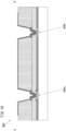
- FIG. 1 schematically explains the configuration of the RTD in the present embodiment.
- FIG. 1 is a schematic cross-sectional view of an RTD 1 according to the present embodiment.
- a lower contact layer (n + -InGaAs) 102 is formed on a semiconductor substrate (InP) 100.
- a compound semiconductor mesa structure (hereinafter referred to as "mesa structure") 120 is formed on the lower contact layer 102.
- the mesa structure 120 has a semiconductor layer 130 including a lower spacer layer (n-InGaAs) 104, a double barrier structure (InAs/InGaAs/InAs) 106, an upper spacer layer (n-InGaAs) 108, and an upper contact layer (n + -InGaAs) 110.
- the compound semiconductor layer 130 includes a heterojunction having a double barrier structure as a multiple barrier structure.
- An upper electrode 112 is arranged above the mesa structure 120 so as to contact the upper surface of the semiconductor layer 130, that is, the upper surface of the upper contact layer 110.
- a lower electrode 116 is arranged so as to be in contact with the lower contact layer 102.
- the entire RTD 1 is covered with a passivation film (dielectric film) 114 so that the upper electrode 112 and the lower electrode 116 are exposed.
- the passivation film 114 is a dielectric film.
- the passivation film 114 preferably comprises any of silicon nitride, silicon oxide, or aluminum oxide.
- the passivation film 114 covers an area ranging from at least the first region 200 to at least a part of the upper electrode 112.
- the first region 200 includes crystal defects, which can be caused by, for example, dry etching.
- the first region 200 can be a region including a crystal, a region including a crystal defect, a region including an amorphous material, a region including both a crystal and a crystal defect, a region including both a crystal and an amorphous material, a region including both a crystal defect and an amorphous material, or a region including a crystal, an amorphous material, and a crystal defect. Details of the first region 200 will be described hereinbelow.
- the passivation film 114 may be arranged in the order of the semiconductor substrate 100, the lower contact layer 102, and the passivation film 114 to cover the lower contact layer 102. Also, in the present embodiment, part of the electrode 118 can function as the upper electrode 112. The electrode 118 extends from above the mesa structure 120 to above the passivation film 114.
- FIG. 2 is an enlarged view of the portion surrounded by circle A in FIG. 1 , and schematically shows the configuration of the outer edge portion of the mesa structure 120 of the RTD 1 in the present embodiment.
- the first region 200 including crystal defects caused by dry etching is generated in the outer edge portion of the semiconductor layer 130 of the mesa structure 120 formed by the dry etching method.
- the first region 200 including crystal defects caused by dry etching is also generated in the outer edge portion of the double barrier structure 106. Therefore, in the first region 200 including crystal defects caused by dry etching, an energy level called a resonance level is not formed, and a current is more likely to flow than in a first region not including crystal defects (a region in which a resonance level is formed).
- the upper electrode 112 and the first region 200 including crystal defects caused by dry etching are arranged apart from each other. Therefore, no current flows through the first region 200 including crystal defects caused by dry etching, and the current flows through the double barrier structure 106 having no crystal defects. As a result, the resonant tunneling effect can be stably obtained with the RTD 1.
- the mesa structure 120 is formed by dry etching as a mesa structure with a mesa diameter of 1 ⁇ m and a mesa height of 0.15 ⁇ m in the RTD 1.
- the first region 200 including crystal defects caused by dry etching is formed within a region having a thickness of 20 nm from the outer edge of the mesa structure 120 toward the center.
- the arrangement be such that the difference between the outer diameter of the electrode 112 and the outer diameter of the upper portion of the mesa structure 120 is 20 nm or more. That is, as shown in FIG. 2 , in a cross section parallel to the thickness direction of the substrate 100 (vertical direction on the paper surface), the outer edge of the upper surface of the mesa structure 120 is arranged at a predetermined distance (distance d in the figure) in a direction perpendicular to the thickness direction of the substrate 100 (in the horizontal direction of the paper surface) from the outer edge of the electrode 112.
- the predetermined distance is 20 nm or more.
- FIG. 3 shows a graph of the voltage-current characteristic of the RTD 1 when the electrode 112 and the first region 200 formed in the mesa structure 120 and including crystal defects caused by dry etching are arranged apart from each other.
- FIG. 3 also shows a graph of the voltage-current characteristic of the RTD 1 when the electrode 112 and the first region 200 formed in the mesa structure 120 and including crystal defects caused by dry etching are not arranged apart from each other.
- a characteristic curve 300 shows the voltage-current characteristic of the RTD 1 in which the electrode 112 and the first region 200 formed in the mesa structure 120 and including crystal defects caused by dry etching are arranged apart from each other.
- a characteristic curve 302 shows the voltage-current characteristics of the RTD 1 in a case where it is assumed that the electrode 112 and the first region 200 formed in the mesa structure 120 and including crystal defects caused by dry etching are not arranged apart from each other.
- the characteristic curve 300 exhibits negative resistance characteristics due to the resonant tunneling effect.
- the characteristic curve 302 shows a so-called short-circuit characteristic in which the resonant tunneling effect is not demonstrated, the current increases as the voltage rises, and the current flows through the first region including crystal defects.
- a characteristic curve 304 shows the voltage-current characteristic of the RTD 1 related to the case where it is assumed that the electrode 112 and the first region 200 formed in the mesa structure 120 and including crystal defects caused by dry etching are not arranged apart from each other, this case being different from that of the characteristic curve 302.
- the current abruptly increases at a certain voltage value (in the case shown in the figure, a voltage value between 0.4 V and 0.5 V), and where a voltage is applied to the RTD 1, a short-circuit characteristic similar to the characteristic curve 302 is shown.
- a case is assumed in which the electrode 112 and the first region 200 including crystal defects caused by dry etching and occurring in the mesa structure 120 and not arranged apart from each other.
- the RTD 1 that operates stably can be obtained by arranging the upper electrode 112 and the first region 200 formed in the semiconductor layer 130 of the mesa structure 120 and including crystal defects caused by dry etching apart from each other.
- FIGS. 4A to 4E schematically illustrate methods for manufacturing the mesa structure 120 of the RTD 1 according to the present embodiment.
- layers are sequentially formed on an n-type InP substrate 100.
- the layers formed are an n + -type InGaAs lower contact layer 102, an undoped InGaAs spacer layer 104, and an undoped AlAs/InGaAs/AlAs double barrier structure 106.
- a non-doped InGaAs spacer layer 108 and an n + -type InGaAs upper contact layer 110 are formed on the double barrier structure 106.
- Each layer is formed by epitaxial growth by a molecular beam epitaxy (MBE) method.
- MBE molecular beam epitaxy
- Each layer may also be formed by epitaxial growth by a metal organic chemical vapor deposition (MOCVD) method or the like. Thereafter, an upper electrode 112 made of a tungsten layer, which is an ohmic electrode material, is formed by sputtering. Subsequently, a silicon oxide layer 400, which serves as a mask during dry etching, is deposited using a plasma enhanced chemical vapor deposition (PECVD) method.
- PECVD plasma enhanced chemical vapor deposition
- a resist pattern 402 is formed using photolithography, and then the silicon oxide layer 400 is processed by dry etching using a fluorine-based gas. Subsequently, the resist pattern 402 is removed (not shown).
- the upper electrode 112 is processed by a dry etching method using a fluorine-based gas.
- the upper contact layer 110, the upper spacer layer 108, the double barrier structure 106, the lower spacer layer 104, and the lower contact layer 102 are processed by dry etching using a chlorine-based gas.
- side etching occurs on the sidewalls of the processed tungsten layer 412.
- side etching occurs on the side wall of the processed tungsten layer 412 as a result of setting the dry etching condition to promote a chemical reaction between chlorine-based radicals based on the chlorine-based gas and tungsten.
- the upper electrode 112 and the center (central axis AX) of the mesa structure 120 are substantially aligned as shown in FIG. 4F. Furthermore, the distance between the outer edge portion of the electrode 112 and the outer edge portion of the mesa structure 120 is 20 nm or more. Thus, the mesa structure 120 is formed in which the upper electrode 112 and the first region 200 containing crystal defects caused by dry etching are set apart from each other.
- FIG. 5 schematically shows the positional relationship between the upper electrode 112 and the semiconductor layer 130 when viewed from the top of the substrate 100 of the RTD 1.
- components other than the substrate 100, the semiconductor layer 130, and the upper electrode 112 are omitted.
- the centers (central axis AX) of the electrode 112 and the semiconductor layer 130 are substantially aligned when viewed from the top of the substrate 100.
- a mesa structure in which the outer edge of the electrode 112 and the outer edge of the semiconductor layer 130 are set apart from each other can be formed.
- a high current density of the order of 10 5 A/cm 2 to 10 6 A/cm 2 can be stably applied to the mesa structure 120.
- a silicon nitride layer is deposited as a passivation film (dielectric layer) 114, and then the lower contact layer 102 is exposed.
- the lower electrode 116 is formed using photolithography and dry etching. After that, an opening is formed in the passivation film 114 above the mesa structure 120 using lithography and dry etching to expose the upper electrode 112 made of the tungsten layer.
- a second Au/Ti electrode (electrode 118 in FIG. 1 ), which serves as a wiring electrode or pad electrode connected to the upper electrode 112, is formed by lithography, electron beam deposition, and lift-off.
- the steps and method for fabricating the RTD described herein are merely an example, and other steps and methods may be employed as long as the above configuration is obtained.
- the InGaAs/InAs-based RTD formed on the InP substrate has been described in the present embodiment, this configuration is not limiting.
- the above configuration and effect can be obtained with a GaAs/AlGaAs-based RTD formed on a GaAs substrate, a GaN/AlGaN-based RTD formed on a GaN substrate or a Si substrate, and a Si/SiGe-based RTD formed on a Si substrate.
- tungsten is used as the upper electrode 112, but this feature is not limiting.
- the above configuration and effect can be obtained with molybdenum and tantalum.
- the RTD is not short-circuited, and it is possible to provide an RTD capable of stably demonstrating a negative resistance characteristic.
- FIG. 6 shows a cross-sectional schematic diagram of an RTD 1 in which two mesa structures 120 are arranged.
- the upper electrode 112 and the first region 200 including crystal defects caused by dry etching are set apart from each other in the same manner as in Embodiment 1.
- the current does not flow through the first region 200, which includes crystal defects caused by dry etching and in which the current is likely to flow, and the current flows through the region including the double barrier structure 106 without crystal defects.
- the RTD 1 of the present embodiment also can stably exhibit the resonant tunneling effect as in Embodiment 1.
- the RTD 1 can be manufactured according to the manufacturing method described in Embodiment 1.
- An oscillator can be configured by connecting the RTD 1 described in Embodiment 1 to an external resonator. Therefore, in Embodiment 3, a resonant tunneling diode (RTD ) terahertz oscillator is described in which one RTD and a patch antenna (microstrip antenna) as an external resonator are connected and integrated to configure a small-sized solid-state element structure.
- RTD tunneling diode
- FIG. 7 is a schematic perspective view illustrating the configuration of the RTD terahertz oscillator according to the present embodiment
- FIG. 8 is a schematic cross-sectional view thereof, which is a cross-sectional view taken along line A-A' in FIG. 8 .
- the configuration of an RTD terahertz oscillator 600 will be described hereinbelow with reference to FIG. 7 .
- the RTD terahertz oscillator 600 has a resonator 602 for generating a terahertz wave and a bias circuit 604 as main components.
- the resonator 602 also includes an RTD 606 and a patch antenna 608.
- the resonator 602 is configured of the semiconductor substrate 100, the lower contact layer 102, a semiconductor layer 700, the first upper electrode 112, the first dielectric layer 114, the lower electrode 116, a second dielectric layer 702, the second upper electrode 118, a third dielectric layer 704, and the patch antenna 608.
- the semiconductor layer 700 includes the lower spacer layer 104, the double barrier structure 106, the upper spacer layer 108, and the upper contact layer 110 shown in FIG. 1 .
- the arrangement of these layers constituting the semiconductor layer 700 is the same as that shown in FIG. 2 .
- the patch antenna 608 corresponds to the third upper electrode.
- the RTD 606 comprises the lower contact layer 102, the semiconductor layer 700, the first upper electrode 112, the first dielectric layer 114, the lower electrode 116, and the second upper electrode 118.
- the mesa structure of the RTD 606 is configured of the semiconductor layer 700 and the first upper electrode 112, and in this mesa structure, the outer edge of the first region 200 including crystal defects caused by dry etching in the semiconductor layer 700 and the outer edge of the upper electrode 112 are arranged at a predetermined distance from each other, in the same manner as in FIG. 2 .
- the RTD terahertz oscillator 600 has a gain in the terahertz wave frequency band.
- the resonator 602 is configured such that the two conductors of the lower electrode 116 and the third upper electrode 608 sandwich the second dielectric layer 702 and the third dielectric layer 704.
- Such a configuration is known as a microstrip type resonator. Therefore, in the present embodiment, a case where the patch antenna 608, which is a typical microstrip resonator, is used will be described.
- the lower electrode 116 is formed on the lower contact layer 102 formed on the semiconductor substrate 100. Further, the semiconductor layer 700 formed on the lower contact layer 102 is electrically connected through the first upper electrode 112, the second upper electrode 118 and the third upper electrode (patch antenna) 608. From the viewpoint of suppressing loss, that is, increasing output and suppressing parasitic oscillation, it is preferable that low-resistance ohmic connection be realized for the lower electrode 116, which is connected to the lower contact layer 102, and the first upper electrode 112, which is connected to the semiconductor layer 700 (upper contact layer 110). In Embodiment 1, it has been assumed that the n + -type InGaAs lower contact layer and the n + -type InGaAs upper contact layer are used.
- the lower electrode 102 and the upper electrode 112 comprise Au (gold) and Ti (titanium), Au and Pd (palladium) and Ti, Au and Pt (platinum) and Ti, W (tungsten), Mo (molybdenum), or Ta (tantalum).
- the RTD 1 is formed by using the upper electrode 112 configured as described above and using the manufacturing method described in Embodiment 1 for the mesa structure.
- the mesa structure 120 can be formed such that the first region including crystal defects caused by dry etching in the semiconductor layer 700 and the upper electrode 112 are set apart from each other.
- the mesa structure 120 of the RTD 606 have a cylindrical structure with a diameter of about 0.5 ⁇ m to 5 ⁇ m.
- three dielectrics are used from the following viewpoints.
- the first dielectric layer 114 and the second dielectric layer 702 are preferably formed using an inorganic dielectric material such as silicon nitride, silicon oxide, or aluminum oxide from the viewpoint of insulation, barrier properties (electrode metal diffusion prevention), and submicron processability.
- an inorganic dielectric material such as silicon nitride, silicon oxide, or aluminum oxide from the viewpoint of insulation, barrier properties (electrode metal diffusion prevention), and submicron processability.
- the third dielectric layer 704 preferably has a thick configuration. However, where the third dielectric layer 704 is too thick, multimode resonance may occur, so the thickness is preferably ⁇ /10 ( ⁇ : effective wavelength of 0-order mode terahertz wave) or less. Further, from the viewpoint of impedance matching with the space (atmosphere), a material with a small dielectric constant is preferable. From the above viewpoint, the third dielectric layer 704 is preferably made of a material having a lower dielectric constant than the material of the second dielectric layer, and is preferably an organic dielectric material as BCB (benzocyclobutene) or a polyimide which are materials having high processability in a semiconductor processing process.
- BCB benzocyclobutene
- the length (width) of the patch antenna 608 in the AA' direction (resonance direction) shown in FIGS. 7 and 8 is set such as to obtain a ⁇ /2 resonator ( ⁇ : effective wavelength of 0-order mode terahertz wave).
- the patch antenna 608 is preferably a 170 ⁇ m square (when the effective wavelength is 340 ⁇ m).
- the RTD 606 is preferably arranged at a position shifted by 34 ⁇ m (when the effective wavelength is 340 ⁇ m) in the resonance direction (AA' direction) from the center of gravity (center) of the patch antenna 608 when viewed from the top of the substrate 100.
- the patch antenna 608 is connected to the RTD 606 through the second upper electrode 118, but the patch antenna 608 and the RTD 606 may be directly connected, rather than through the second upper electrode 118.
- the second upper electrode be formed on the second dielectric 702 made of an inorganic material, and then the third dielectric 704 made of an organic material be formed.
- the patch antenna (third upper electrode) 608 is thus configured.
- the RTD 606 is supplied with power via the patch antenna (third upper electrode) 608, but this feature is not limiting, and a power supply line may be formed on the second dielectric layer 702.
- the patch antenna is used as an antenna, but such feature is not limiting, and a slot antenna, a throttle ring antenna, a tapered slot antenna, a ring antenna, or the like may be configured.
- FIG. 9 is a schematic perspective view illustrating the configuration of the RTD terahertz oscillator according to the present embodiment
- FIG. 10 is a schematic cross-sectional view thereof, which is a cross-sectional view taken along line A-A' in FIG. 9 .
- the number of RTDs 606 is increased, as in the present embodiment, the current flowing through the resonator 602 can be increased, and the output of the oscillator can be increased.
- the configuration of the RTD terahertz oscillator 800 having a plurality of RTDs 606 in the present embodiment is basically the same as in Embodiment 3, but the positional relationship between the RTDs 606 and the patch antenna 608 is different from that in Embodiment 3.
- the patch antenna 608 is assumed to be a 170 ⁇ m square (when the effective wavelength is 340 ⁇ m).
- the oscillator according to the present embodiment has a plurality of oscillators according to Embodiment 3, and the plurality of oscillators are coupled to operate in synchronization with each other.
- the patch antenna is used as an antenna, but such feature is not limiting, and a slot antenna, a throttle ring antenna, a tapered slot antenna, a ring antenna, or the like may be configured.
- the RTDs can oscillate with mutual injection synchronization.
- the RTDs described in the above embodiments can be adopted in, for example, a detection system. Accordingly, the detection system according to the present embodiment will be described with reference to FIG. 11 .
- the detection system may be a system capable of capturing images, for example a camera system.
- a camera system will be described as an example.
- FIG. 11 is a schematic diagram for explaining the configuration of a camera system 2300 using terahertz waves.
- the camera system 2300 has an oscillation device 2301, a detection device 2302 and a processing unit 2303.
- the RTD described in each embodiment can be used as an oscillation element.
- the detection device 2302 has a receiving element that receives the high-frequency terahertz waves transmitted from the oscillation device 2301. In this way, the detection device 2302 can detect electromagnetic waves transmitted from an antenna device, and may be, for example, an antenna device using other semiconductor elements such as a Schottky barrier diode.
- the terahertz wave transmitted from the oscillation device 2301 is reflected by an object 2305 and detected by the detection device 2302.
- the processing unit 2303 has a processing circuit that processes the signal detected by the detection device 2302. Image data generated by the processing unit 2303 are output from an output unit 2304. With such a configuration, the camera system 2300 can acquire terahertz images.
- the oscillation device 2301 or the detection device 2302 may be provided with an optical section having a lens through which terahertz waves can pass.
- the optical section includes at least one material transparent to terahertz waves, such as polyethylene, Teflon (registered trademark), high-resistance silicon, and a polyolefin resin, and may be composed of multiple layers.
- the camera system described in the present embodiment is merely an example, and may be in other forms.
- the information acquired by the system is not limited to image information, and the detection system may detect signals.
- a resonant tunneling diode includes a substrate, and a mesa structure including a compound semiconductor layer including a heterojunction comprising a multi-barrier structure disposed on the substrate, and an electrode disposed on the upper surface of the compound semiconductor layer.
- An outer edge portion of the compound semiconductor layer is a first region including crystal defects, and the first region and the electrode are set apart from each other.
Landscapes
- Light Receiving Elements (AREA)
- Variable-Direction Aerials And Aerial Arrays (AREA)
Abstract
Description
- The technique of the present disclosure relates to a resonant tunneling diode, an oscillator, and a detection system.
- Terahertz oscillators in which a resonant tunneling diode (RTDs) and an antenna are integrated are being developed for imaging systems using terahertz waves and large-capacity wireless communication systems.
- For example,
Japanese Patent Application Publication No. 2020-57739 - In view of the above, the technique of the present disclosure provides a resonant tunneling diode that operates stably without short-circuiting in the characteristics of the resonant tunneling diode when a current is applied.
- According to an aspect of the present disclosure, it is provided a resonant tunneling diode as specified in
claim 1. - According to an aspect of the present disclosure, it is provided an oscillator as specified in claim 10.
- According to an aspect of the present disclosure, it is provided an oscillator, as specified in claim 11.
- According to an aspect of the present disclosure, it is provided a detection system as specified in claim 12.
- Further features of the present invention will become apparent from the following description of exemplary embodiments with reference to the attached drawings.
-
-
FIG. 1 schematically illustrates the configuration of an RTD according toEmbodiment 1; -
FIG. 2 schematically explains the configuration of an RTD mesa structure side wall according toEmbodiment 1; -
FIG. 3 explains the characteristics of the RTD according toEmbodiment 1; -
FIGS. 4A to 4E schematically explain methods of manufacturing the RTD mesa structure according toEmbodiment 1; -
FIG. 5 schematically explains the configuration of the RTD according toEmbodiment 1; -
FIG. 6 schematically illustrates the configuration of an RTD according to Embodiment 2 in which two mesa structures are arranged; -
FIG. 7 is a schematic perspective view illustrating the configuration of an RTD terahertz oscillator according to Embodiment 3; -
FIG. 8 is a schematic cross-sectional view for explaining the configuration of the RTD terahertz oscillator according to Embodiment 3; -
FIG. 9 is a schematic perspective view illustrating the configuration of the RTD terahertz oscillator according toEmbodiment 4; -
FIG. 10 is a schematic cross-sectional view for explaining the configuration of the RTD terahertz oscillator according toEmbodiment 4; and -
FIG. 11 schematically explains the configuration of the detection system according to Embodiment 5. - In order to realize an RTD terahertz oscillator, it is necessary to apply a high current density of the order of 105 A/cm2 to 106 A/cm2 to the RTD. In order to achieve this high current density, it is necessary to process a compound semiconductor epitaxial wafer to form a mesa structure having a multiple barrier structure and a diameter of about 0.5 µm to 5 µm.
- The multiple barrier structure can be exemplified by a double barrier structure in which a quantum well layer with a small bandgap is sandwiched between barrier layers with a large bandgap. A mesa structure of this size is typically fabricated using a dry etching method.
- The inventors of the present application finds the following points after examination. Firstly, when a compound semiconductor epitaxial layer (compound semiconductor single crystal layer) is processed by a dry etching method, the surface region (a region of several tens of nanometers) of the semiconductor crystal layer left by etching is considerably damaged. This region could have more crystal defects than an undamaged semiconductor crystal layer.
- Secondly, a region including many crystal defects could be formed in the outer edge portion of the mesa structure with a diameter of about 0.5 µm to 5 µm, which is formed by dry etching to realize an RTD terahertz oscillator. For this reason, a problem arising when a current is injected into a region including many crystal defects is that the barrier layers and quantum well layers of the multiple barrier structure collapse, the RTD does not exhibit a negative resistance characteristic resulting from the resonant tunneling effect, and current short-circuiting occurs. For example, a high current density of the order of 105 A/cm2 to 106 A/cm2 is applied to the mesa having a diameter of about 0.5 µm to 5 µm, the current short-circuiting could occurs.
- Preferred embodiments of the technique of the present disclosure will be described below with reference to the drawings. Each drawing is only described for the purpose of explaining the structure or configuration, and the dimensions of each member shown in the drawing do not necessarily reflect the actual dimensions. In addition, in each figure, the same reference numerals are given to the same members or the same constituent elements, and hereinafter, descriptions of overlapping contents will be omitted. For example, in the following embodiments, a resonant tunneling diode is shown as an example of a semiconductor device to which the present invention can be applied, but the present invention can also be applied to light-emitting devices such as surface emitting lasers and light-emitting diodes.
- According to the technique of the present disclosure, when arranging an electrode in contact with a compound semiconductor mesa structure on the mesa structure, a structure is configured in which, by contrast with the structure of the conventional example, a first region including a crystal defect formed in the mesa structure and the electrode are arranged apart from each other. In other words, a configuration is employed in which the outer diameter of the electrode placed in contact with the compound semiconductor mesa structure is smaller than the outer diameter of the upper portion of the compound semiconductor mesa structure. Embodiments of the technique of the present disclosure will be described below.
- In
Embodiment 1, a single resonant tunneling diode (RTD) will be described.FIG. 1 schematically explains the configuration of the RTD in the present embodiment. -
FIG. 1 is a schematic cross-sectional view of anRTD 1 according to the present embodiment. As shown in the figure, a lower contact layer (n+-InGaAs) 102 is formed on a semiconductor substrate (InP) 100. A compound semiconductor mesa structure (hereinafter referred to as "mesa structure") 120 is formed on thelower contact layer 102. Themesa structure 120 has asemiconductor layer 130 including a lower spacer layer (n-InGaAs) 104, a double barrier structure (InAs/InGaAs/InAs) 106, an upper spacer layer (n-InGaAs) 108, and an upper contact layer (n+-InGaAs) 110. Thus, the compound semiconductor layer (hereinafter referred to as "semiconductor layer") 130 includes a heterojunction having a double barrier structure as a multiple barrier structure. Anupper electrode 112 is arranged above themesa structure 120 so as to contact the upper surface of thesemiconductor layer 130, that is, the upper surface of theupper contact layer 110. Further, alower electrode 116 is arranged so as to be in contact with thelower contact layer 102. Furthermore, theentire RTD 1 is covered with a passivation film (dielectric film) 114 so that theupper electrode 112 and thelower electrode 116 are exposed. Thepassivation film 114 is a dielectric film. For example, thepassivation film 114 preferably comprises any of silicon nitride, silicon oxide, or aluminum oxide. Thepassivation film 114 covers an area ranging from at least thefirst region 200 to at least a part of theupper electrode 112. Thefirst region 200 includes crystal defects, which can be caused by, for example, dry etching. For example, thefirst region 200 can be a region including a crystal, a region including a crystal defect, a region including an amorphous material, a region including both a crystal and a crystal defect, a region including both a crystal and an amorphous material, a region including both a crystal defect and an amorphous material, or a region including a crystal, an amorphous material, and a crystal defect. Details of thefirst region 200 will be described hereinbelow. Also, thepassivation film 114 may be arranged in the order of thesemiconductor substrate 100, thelower contact layer 102, and thepassivation film 114 to cover thelower contact layer 102. Also, in the present embodiment, part of theelectrode 118 can function as theupper electrode 112. Theelectrode 118 extends from above themesa structure 120 to above thepassivation film 114. -
FIG. 2 is an enlarged view of the portion surrounded by circle A inFIG. 1 , and schematically shows the configuration of the outer edge portion of themesa structure 120 of theRTD 1 in the present embodiment. As shown inFIG. 2 , thefirst region 200 including crystal defects caused by dry etching is generated in the outer edge portion of thesemiconductor layer 130 of themesa structure 120 formed by the dry etching method. Thefirst region 200 including crystal defects caused by dry etching is also generated in the outer edge portion of thedouble barrier structure 106. Therefore, in thefirst region 200 including crystal defects caused by dry etching, an energy level called a resonance level is not formed, and a current is more likely to flow than in a first region not including crystal defects (a region in which a resonance level is formed). However, as shown inFIG. 2 , theupper electrode 112 and thefirst region 200 including crystal defects caused by dry etching are arranged apart from each other. Therefore, no current flows through thefirst region 200 including crystal defects caused by dry etching, and the current flows through thedouble barrier structure 106 having no crystal defects. As a result, the resonant tunneling effect can be stably obtained with theRTD 1. - For example, a case is assumed in which the
mesa structure 120 is formed by dry etching as a mesa structure with a mesa diameter of 1 µm and a mesa height of 0.15 µm in theRTD 1. In this case, it can be considered that thefirst region 200 including crystal defects caused by dry etching is formed within a region having a thickness of 20 nm from the outer edge of themesa structure 120 toward the center. - Therefore, in order to prevent current from flowing through the
first region 200 including crystal defects caused by dry etching, it is preferable that the arrangement be such that the difference between the outer diameter of theelectrode 112 and the outer diameter of the upper portion of themesa structure 120 is 20 nm or more. That is, as shown inFIG. 2 , in a cross section parallel to the thickness direction of the substrate 100 (vertical direction on the paper surface), the outer edge of the upper surface of themesa structure 120 is arranged at a predetermined distance (distance d in the figure) in a direction perpendicular to the thickness direction of the substrate 100 (in the horizontal direction of the paper surface) from the outer edge of theelectrode 112. Here, the predetermined distance is 20 nm or more. -
FIG. 3 shows a graph of the voltage-current characteristic of theRTD 1 when theelectrode 112 and thefirst region 200 formed in themesa structure 120 and including crystal defects caused by dry etching are arranged apart from each other.FIG. 3 also shows a graph of the voltage-current characteristic of theRTD 1 when theelectrode 112 and thefirst region 200 formed in themesa structure 120 and including crystal defects caused by dry etching are not arranged apart from each other. InFIG. 3 , acharacteristic curve 300 shows the voltage-current characteristic of theRTD 1 in which theelectrode 112 and thefirst region 200 formed in themesa structure 120 and including crystal defects caused by dry etching are arranged apart from each other. Acharacteristic curve 302 shows the voltage-current characteristics of theRTD 1 in a case where it is assumed that theelectrode 112 and thefirst region 200 formed in themesa structure 120 and including crystal defects caused by dry etching are not arranged apart from each other. Thus, thecharacteristic curve 300 exhibits negative resistance characteristics due to the resonant tunneling effect. Meanwhile, thecharacteristic curve 302 shows a so-called short-circuit characteristic in which the resonant tunneling effect is not demonstrated, the current increases as the voltage rises, and the current flows through the first region including crystal defects. - Furthermore, a characteristic curve 304 shows the voltage-current characteristic of the
RTD 1 related to the case where it is assumed that theelectrode 112 and thefirst region 200 formed in themesa structure 120 and including crystal defects caused by dry etching are not arranged apart from each other, this case being different from that of thecharacteristic curve 302. In the characteristic curve 304, the current abruptly increases at a certain voltage value (in the case shown in the figure, a voltage value between 0.4 V and 0.5 V), and where a voltage is applied to theRTD 1, a short-circuit characteristic similar to thecharacteristic curve 302 is shown. A case is assumed in which theelectrode 112 and thefirst region 200 including crystal defects caused by dry etching and occurring in themesa structure 120 and not arranged apart from each other. In this case, an unstable operation occurs, such as theRTD 1 not exhibiting the resonant tunneling effect, or theRTD 1 not exhibiting the resonant tunneling effect when driven continuously. Therefore, with theRTD 1 of the present embodiment, theRTD 1 that operates stably can be obtained by arranging theupper electrode 112 and thefirst region 200 formed in thesemiconductor layer 130 of themesa structure 120 and including crystal defects caused by dry etching apart from each other. -
FIGS. 4A to 4E schematically illustrate methods for manufacturing themesa structure 120 of theRTD 1 according to the present embodiment. As shown inFIG. 4A , first, layers are sequentially formed on an n-type InP substrate 100. The layers formed are an n+-type InGaAslower contact layer 102, an undopedInGaAs spacer layer 104, and an undoped AlAs/InGaAs/AlAsdouble barrier structure 106. Furthermore, a non-dopedInGaAs spacer layer 108 and an n+-type InGaAsupper contact layer 110 are formed on thedouble barrier structure 106. Each layer is formed by epitaxial growth by a molecular beam epitaxy (MBE) method. Each layer may also be formed by epitaxial growth by a metal organic chemical vapor deposition (MOCVD) method or the like. Thereafter, anupper electrode 112 made of a tungsten layer, which is an ohmic electrode material, is formed by sputtering. Subsequently, asilicon oxide layer 400, which serves as a mask during dry etching, is deposited using a plasma enhanced chemical vapor deposition (PECVD) method. - Next, as shown in
FIG. 4B , a resistpattern 402 is formed using photolithography, and then thesilicon oxide layer 400 is processed by dry etching using a fluorine-based gas. Subsequently, the resistpattern 402 is removed (not shown). - Next, as shown in
FIG. 4C , using a processedsilicon oxide layer 404 as a mask, theupper electrode 112 is processed by a dry etching method using a fluorine-based gas. - Next, as shown in
FIG. 4D , using the processedsilicon oxide layer 404 as a mask, theupper contact layer 110, theupper spacer layer 108, thedouble barrier structure 106, thelower spacer layer 104, and thelower contact layer 102 are processed by dry etching using a chlorine-based gas. At this time, by adjusting the dry etching conditions, side etching occurs on the sidewalls of the processedtungsten layer 412. Specifically, side etching occurs on the side wall of the processedtungsten layer 412 as a result of setting the dry etching condition to promote a chemical reaction between chlorine-based radicals based on the chlorine-based gas and tungsten. - Next, where the processed
silicon oxide layer 404 is removed as shown inFIG. 4E , theupper electrode 112 and the center (central axis AX) of themesa structure 120 are substantially aligned as shown in FIG. 4F. Furthermore, the distance between the outer edge portion of theelectrode 112 and the outer edge portion of themesa structure 120 is 20 nm or more. Thus, themesa structure 120 is formed in which theupper electrode 112 and thefirst region 200 containing crystal defects caused by dry etching are set apart from each other. - By continuously performing the step explained in
FIG. 4C and the step explained inFIG. 4D and using the same processedsilicon oxide layer 404, the centers of theupper electrode 112 and thesemiconductor layer 130 can be substantially aligned with each other when viewed from the top of thesubstrate 100.FIG. 5 schematically shows the positional relationship between theupper electrode 112 and thesemiconductor layer 130 when viewed from the top of thesubstrate 100 of theRTD 1. InFIG. 5 , components other than thesubstrate 100, thesemiconductor layer 130, and theupper electrode 112 are omitted. As shown inFIG. 5 , the centers (central axis AX) of theelectrode 112 and thesemiconductor layer 130 are substantially aligned when viewed from the top of thesubstrate 100. By adopting such a configuration in which the central axis of theupper electrode 112 and the center of thesemiconductor layer 130 are substantially aligned, a mesa structure in which the outer edge of theelectrode 112 and the outer edge of thesemiconductor layer 130 are set apart from each other can be formed. As a result, in theRTD 1 of the present embodiment, a high current density of the order of 105 A/cm2 to 106 A/cm2 can be stably applied to themesa structure 120. - Also, although not shown in
FIGS. 4A to 4E , as a step after forming themesa structure 120, a silicon nitride layer is deposited as a passivation film (dielectric layer) 114, and then thelower contact layer 102 is exposed. Subsequently, after forming a tungsten layer, thelower electrode 116 is formed using photolithography and dry etching. After that, an opening is formed in thepassivation film 114 above themesa structure 120 using lithography and dry etching to expose theupper electrode 112 made of the tungsten layer. After that, a second Au/Ti electrode (electrode 118 inFIG. 1 ), which serves as a wiring electrode or pad electrode connected to theupper electrode 112, is formed by lithography, electron beam deposition, and lift-off. - Through the above steps, it is possible to form the
RTD 1 shown inFIG. 1 . The steps and method for fabricating the RTD described herein are merely an example, and other steps and methods may be employed as long as the above configuration is obtained. In addition, although the InGaAs/InAs-based RTD formed on the InP substrate has been described in the present embodiment, this configuration is not limiting. For example, the above configuration and effect can be obtained with a GaAs/AlGaAs-based RTD formed on a GaAs substrate, a GaN/AlGaN-based RTD formed on a GaN substrate or a Si substrate, and a Si/SiGe-based RTD formed on a Si substrate. Further, in the explanation of the present embodiment, tungsten is used as theupper electrode 112, but this feature is not limiting. For example, the above configuration and effect can be obtained with molybdenum and tantalum. - Therefore, according to the present embodiment, even if a high current density of the order of 105 A/cm2 to 106 A/cm2 is applied to the mesa having a diameter of about 0.5 µm to 5 µm, the RTD is not short-circuited, and it is possible to provide an RTD capable of stably demonstrating a negative resistance characteristic.
- Next, the
RTD 1 according to Embodiment 2 will be described. In the following explanation, descriptions of the same configurations and processes as those ofEmbodiment 1 are omitted. - The configuration of the
RTD 1 in which asingle mesa structure 120 is provided on thesubstrate 100 has been described inEmbodiment 1, but anRTD 1 having an RTD array configuration in which a plurality ofmesa structures 120 is arranged on thesubstrate 100 can also be manufactured.FIG. 6 shows a cross-sectional schematic diagram of anRTD 1 in which twomesa structures 120 are arranged. As shown inFIG. 6 , in eachmesa structure 120 in the array configuration as well, theupper electrode 112 and thefirst region 200 including crystal defects caused by dry etching are set apart from each other in the same manner as inEmbodiment 1. Therefore, the current does not flow through thefirst region 200, which includes crystal defects caused by dry etching and in which the current is likely to flow, and the current flows through the region including thedouble barrier structure 106 without crystal defects. As a result, theRTD 1 of the present embodiment also can stably exhibit the resonant tunneling effect as inEmbodiment 1. TheRTD 1 can be manufactured according to the manufacturing method described inEmbodiment 1. - An oscillator can be configured by connecting the
RTD 1 described inEmbodiment 1 to an external resonator. Therefore, in Embodiment 3, a resonant tunneling diode (RTD ) terahertz oscillator is described in which one RTD and a patch antenna (microstrip antenna) as an external resonator are connected and integrated to configure a small-sized solid-state element structure. -
FIG. 7 is a schematic perspective view illustrating the configuration of the RTD terahertz oscillator according to the present embodiment, andFIG. 8 is a schematic cross-sectional view thereof, which is a cross-sectional view taken along line A-A' inFIG. 8 . - The configuration of an
RTD terahertz oscillator 600 will be described hereinbelow with reference toFIG. 7 . TheRTD terahertz oscillator 600 has aresonator 602 for generating a terahertz wave and abias circuit 604 as main components. Theresonator 602 also includes anRTD 606 and apatch antenna 608. - Next, the
resonator 602 will be explained usingFIG. 8 . Theresonator 602 is configured of thesemiconductor substrate 100, thelower contact layer 102, asemiconductor layer 700, the firstupper electrode 112, thefirst dielectric layer 114, thelower electrode 116, asecond dielectric layer 702, the secondupper electrode 118, a thirddielectric layer 704, and thepatch antenna 608. Thesemiconductor layer 700 includes thelower spacer layer 104, thedouble barrier structure 106, theupper spacer layer 108, and theupper contact layer 110 shown inFIG. 1 . The arrangement of these layers constituting thesemiconductor layer 700 is the same as that shown inFIG. 2 . Also, thepatch antenna 608 corresponds to the third upper electrode. - Further, the
RTD 606 comprises thelower contact layer 102, thesemiconductor layer 700, the firstupper electrode 112, thefirst dielectric layer 114, thelower electrode 116, and the secondupper electrode 118. The mesa structure of theRTD 606 is configured of thesemiconductor layer 700 and the firstupper electrode 112, and in this mesa structure, the outer edge of thefirst region 200 including crystal defects caused by dry etching in thesemiconductor layer 700 and the outer edge of theupper electrode 112 are arranged at a predetermined distance from each other, in the same manner as inFIG. 2 . As a result of employing the above configuration in theRTD 606 according to the present embodiment, theRTD terahertz oscillator 600 has a gain in the terahertz wave frequency band. - Further, the
resonator 602 is configured such that the two conductors of thelower electrode 116 and the thirdupper electrode 608 sandwich thesecond dielectric layer 702 and the thirddielectric layer 704. Such a configuration is known as a microstrip type resonator. Therefore, in the present embodiment, a case where thepatch antenna 608, which is a typical microstrip resonator, is used will be described. - The
lower electrode 116 is formed on thelower contact layer 102 formed on thesemiconductor substrate 100. Further, thesemiconductor layer 700 formed on thelower contact layer 102 is electrically connected through the firstupper electrode 112, the secondupper electrode 118 and the third upper electrode (patch antenna) 608. From the viewpoint of suppressing loss, that is, increasing output and suppressing parasitic oscillation, it is preferable that low-resistance ohmic connection be realized for thelower electrode 116, which is connected to thelower contact layer 102, and the firstupper electrode 112, which is connected to the semiconductor layer 700 (upper contact layer 110). InEmbodiment 1, it has been assumed that the n+-type InGaAs lower contact layer and the n+-type InGaAs upper contact layer are used. Therefore, preferably, thelower electrode 102 and theupper electrode 112 comprise Au (gold) and Ti (titanium), Au and Pd (palladium) and Ti, Au and Pt (platinum) and Ti, W (tungsten), Mo (molybdenum), or Ta (tantalum). TheRTD 1 is formed by using theupper electrode 112 configured as described above and using the manufacturing method described inEmbodiment 1 for the mesa structure. As a result, themesa structure 120 can be formed such that the first region including crystal defects caused by dry etching in thesemiconductor layer 700 and theupper electrode 112 are set apart from each other. In order to obtain an oscillator in the terahertz band, it is preferable that themesa structure 120 of theRTD 606 have a cylindrical structure with a diameter of about 0.5 µm to 5 µm. - In the present embodiment, three dielectrics are used from the following viewpoints.
- The
first dielectric layer 114 and thesecond dielectric layer 702 are preferably formed using an inorganic dielectric material such as silicon nitride, silicon oxide, or aluminum oxide from the viewpoint of insulation, barrier properties (electrode metal diffusion prevention), and submicron processability. By using such materials for thefirst dielectric layer 114 and thesecond dielectric 702, miniaturization and high current density of theRTD 606 can be achieved. As a result, in theRTD 606, the output and frequency of theRTD terahertz resonator 600 can be increased. The reason why the first dielectric and the second dielectric are separated is to form thelower electrode 116 on thelower contact layer 102. - From the viewpoint of radiation efficiency of the
patch antenna 608, the thirddielectric layer 704 preferably has a thick configuration. However, where the thirddielectric layer 704 is too thick, multimode resonance may occur, so the thickness is preferably λ/10 (λ: effective wavelength of 0-order mode terahertz wave) or less. Further, from the viewpoint of impedance matching with the space (atmosphere), a material with a small dielectric constant is preferable. From the above viewpoint, the thirddielectric layer 704 is preferably made of a material having a lower dielectric constant than the material of the second dielectric layer, and is preferably an organic dielectric material as BCB (benzocyclobutene) or a polyimide which are materials having high processability in a semiconductor processing process. - Further, in the
patch antenna 608, the length (width) of thepatch antenna 608 in the AA' direction (resonance direction) shown inFIGS. 7 and8 is set such as to obtain a λ/2 resonator (λ: effective wavelength of 0-order mode terahertz wave). - For example, in the case of an oscillator with a frequency of 0.45 terahertz, the
patch antenna 608 is preferably a 170 µm square (when the effective wavelength is 340 µm). In addition, from the viewpoint of suppressing multimode oscillation, theRTD 606 is preferably arranged at a position shifted by 34 µm (when the effective wavelength is 340 µm) in the resonance direction (AA' direction) from the center of gravity (center) of thepatch antenna 608 when viewed from the top of thesubstrate 100. - In the present embodiment, the
patch antenna 608 is connected to theRTD 606 through the secondupper electrode 118, but thepatch antenna 608 and theRTD 606 may be directly connected, rather than through the secondupper electrode 118. However, from the viewpoint of processing stability or power supply stability to theRTD 606, it is preferable that the second upper electrode be formed on thesecond dielectric 702 made of an inorganic material, and then thethird dielectric 704 made of an organic material be formed. The patch antenna (third upper electrode) 608 is thus configured. - In the present embodiment, the
RTD 606 is supplied with power via the patch antenna (third upper electrode) 608, but this feature is not limiting, and a power supply line may be formed on thesecond dielectric layer 702. In addition, in the present embodiment, the patch antenna is used as an antenna, but such feature is not limiting, and a slot antenna, a throttle ring antenna, a tapered slot antenna, a ring antenna, or the like may be configured. - By adopting the above configuration, it is possible to obtain an RTD that can stably demonstrate a negative resistance characteristic without short-circuiting in the characteristics of the resonant tunneling diode even when a high current density of the order of 105 A/cm2 to 106 A/cm2 is applied to a mesa with a diameter of about 0.5 µm to 5 µm. Therefore, in the present embodiment, it is also possible to provide a small-sized single-solid-state RTD terahertz oscillator that operates stably.
- In Embodiment 3, the
RTD terahertz oscillator 600 having oneRTD 606 has been described, but an oscillator can also be configured by connecting a plurality of RTDs described in Embodiment 2 to an external resonator. Accordingly, inEmbodiment 4, anRTD terahertz oscillator 800 including twoRTDs 606 will be described with reference toFIGS. 9 and10 .FIG. 9 is a schematic perspective view illustrating the configuration of the RTD terahertz oscillator according to the present embodiment, andFIG. 10 is a schematic cross-sectional view thereof, which is a cross-sectional view taken along line A-A' inFIG. 9 . Where the number ofRTDs 606 is increased, as in the present embodiment, the current flowing through theresonator 602 can be increased, and the output of the oscillator can be increased. - The configuration of the
RTD terahertz oscillator 800 having a plurality ofRTDs 606 in the present embodiment is basically the same as in Embodiment 3, but the positional relationship between the RTDs 606 and thepatch antenna 608 is different from that in Embodiment 3. Specifically, for example, in the case of an oscillator with a frequency of 0.45 terahertz, thepatch antenna 608 is assumed to be a 170 µm square (when the effective wavelength is 340 µm). In this case, from the viewpoint of radiation efficiency and suppression of multimode oscillation, it is preferable to arrange twoRTDs substrate 100. In this case, the distance between the twoRTDs - In the present embodiment, the patch antenna is used as an antenna, but such feature is not limiting, and a slot antenna, a throttle ring antenna, a tapered slot antenna, a ring antenna, or the like may be configured.
- By adopting the above configuration, it is possible to obtain an RTD that can stably demonstrate a negative resistance characteristic without short-circuiting in the characteristics of the resonant tunneling diode even when a high current density of the order of 105 A/cm2 to 106 A/cm2 is applied to a mesa with a diameter of about 0.5 µm to 5 µm. Therefore, in the present embodiment, it is also possible to provide a small-sized and high-output RTD terahertz oscillator that operates stably and has a single solid-state element structure.
- Further, by configuring an array resonator in which the
resonators 602 shown inFIG. 8 are arranged in an array (for example, 6 × 6 = 36), it is possible to realize an RTD array terahertz oscillator having a higher output. By coupling a plurality of RTD terahertz resonators constituting an array resonator via a microstrip line, the RTDs can oscillate with mutual injection synchronization. - The RTDs described in the above embodiments can be adopted in, for example, a detection system. Accordingly, the detection system according to the present embodiment will be described with reference to
FIG. 11 . The detection system may be a system capable of capturing images, for example a camera system. In the present embodiment, a camera system will be described as an example.FIG. 11 is a schematic diagram for explaining the configuration of acamera system 2300 using terahertz waves. - The
camera system 2300 has anoscillation device 2301, adetection device 2302 and aprocessing unit 2303. In theoscillation device 2301, the RTD described in each embodiment can be used as an oscillation element. Thedetection device 2302 has a receiving element that receives the high-frequency terahertz waves transmitted from theoscillation device 2301. In this way, thedetection device 2302 can detect electromagnetic waves transmitted from an antenna device, and may be, for example, an antenna device using other semiconductor elements such as a Schottky barrier diode. The terahertz wave transmitted from theoscillation device 2301 is reflected by anobject 2305 and detected by thedetection device 2302. Theprocessing unit 2303 has a processing circuit that processes the signal detected by thedetection device 2302. Image data generated by theprocessing unit 2303 are output from anoutput unit 2304. With such a configuration, thecamera system 2300 can acquire terahertz images. - The
oscillation device 2301 or thedetection device 2302 may be provided with an optical section having a lens through which terahertz waves can pass. The optical section includes at least one material transparent to terahertz waves, such as polyethylene, Teflon (registered trademark), high-resistance silicon, and a polyolefin resin, and may be composed of multiple layers. - The camera system described in the present embodiment is merely an example, and may be in other forms. In particular, the information acquired by the system is not limited to image information, and the detection system may detect signals.
- According to the technique of the present disclosure, it is possible to provide a resonant tunneling diode that can stably operate without short-circuiting in the characteristics of the resonant tunneling diode during current application.
- While the present invention has been described with reference to exemplary embodiments, it is to be understood that the invention is not limited to the disclosed exemplary embodiments. The scope of the following claims is to be accorded the broadest interpretation so as to encompass all such modifications and equivalent structures and functions.
- A resonant tunneling diode includes a substrate, and a mesa structure including a compound semiconductor layer including a heterojunction comprising a multi-barrier structure disposed on the substrate, and an electrode disposed on the upper surface of the compound semiconductor layer. An outer edge portion of the compound semiconductor layer is a first region including crystal defects, and the first region and the electrode are set apart from each other.
Claims (12)
- A resonant tunneling diode comprising:a substrate; anda mesa structure including a compound semiconductor layer including a heterojunction comprising a multi-barrier structure disposed on the substrate, and an electrode disposed on the upper surface of the compound semiconductor layer, whereinan outer edge portion of the compound semiconductor layer is a first region including crystal defects, andthe first region and the electrode are set apart from each other.
- The resonant tunneling diode according to claim 1, wherein
in a cross section parallel to a thickness direction of the substrate, the outer edge of the upper surface of the compound semiconductor layer is separated from the outer edge of the electrode by a predetermined distance in a direction perpendicular to the thickness direction of the substrate. - The resonant tunneling diode of claim 2, wherein the predetermined distance is 20 nm or more.
- The resonant tunneling diode of any one of claims 1 to 3, wherein a center of the electrode and a center of the compound semiconductor layer are substantially aligned in a top view of the substrate.
- The resonant tunneling diode of any one of claims 1 to 4, further comprising a dielectric film covering an area ranging at least from the first region to the electrode.
- The resonant tunneling diode of claim 5, wherein the dielectric film includes silicon nitride, silicon oxide, or aluminum oxide.
- The resonant tunneling diode of any one of claims 1 to 6, wherein the electrode comprises gold and titanium, gold and palladium and titanium, gold and platinum and titanium, tungsten, molybdenum, or tantalum.
- The resonant tunneling diode of any one of claims 1 to 7, wherein the first region including crystal defects includes crystal defects caused by dry etching.
- The resonant tunneling diode of any one of claims 1 to 7, wherein the first region is a region including a crystal, an amorphous material, or both a crystal and an amorphous material.
- An oscillator, comprising:one or a plurality of resonant tunneling diodes according to any one of claims 1 to 9, whereinone or the plurality of resonant tunneling diodes are connected to and integrated with an antenna to form a single solid-state element structure.
- An oscillator, comprising:a plurality of oscillators according to claim 10, whereinthe plurality of oscillators are coupled and operate in synchronization with each other.
- A detection system comprising:the resonant tunneling diode according to any one of claims 1 to 9 as an oscillation element;a receiving element that receives a high frequency from the oscillation element; anda processing circuit that processes a signal from the receiving element.
Applications Claiming Priority (1)
| Application Number | Priority Date | Filing Date | Title |
|---|---|---|---|
| JP2022012278A JP7840704B2 (en) | 2022-01-28 | 2022-01-28 | Resonant tunneling diode, oscillator, detection system, and method for manufacturing a resonant tunneling diode |
Publications (1)
| Publication Number | Publication Date |
|---|---|
| EP4220731A1 true EP4220731A1 (en) | 2023-08-02 |
Family
ID=85132725
Family Applications (1)
| Application Number | Title | Priority Date | Filing Date |
|---|---|---|---|
| EP23153384.5A Pending EP4220731A1 (en) | 2022-01-28 | 2023-01-26 | Resonant tunneling diode, oscillator and detection system |
Country Status (4)
| Country | Link |
|---|---|
| US (1) | US20230246112A1 (en) |
| EP (1) | EP4220731A1 (en) |
| JP (1) | JP7840704B2 (en) |
| CN (1) | CN116525649A (en) |
Families Citing this family (3)
| Publication number | Priority date | Publication date | Assignee | Title |
|---|---|---|---|---|
| US20240120425A1 (en) * | 2022-10-06 | 2024-04-11 | Canon Kabushiki Kaisha | Semiconductor element and terahertz wave system |
| WO2025204759A1 (en) * | 2024-03-28 | 2025-10-02 | ソニーグループ株式会社 | Resonant tunnel diode element and electronic apparatus |
| WO2025204757A1 (en) * | 2024-03-28 | 2025-10-02 | ソニーグループ株式会社 | Resonant tunnel diode element and electronic apparatus |
Citations (2)
| Publication number | Priority date | Publication date | Assignee | Title |
|---|---|---|---|---|
| US20160218201A1 (en) * | 2015-01-22 | 2016-07-28 | Fujitsu Limited | Compound semiconductor device and method for manufacturing the same |
| US20200111929A1 (en) * | 2018-10-04 | 2020-04-09 | Canon Kabushiki Kaisha | Semiconductor element for oscillating or detecting terahertz wave and manufacturing method of semiconductor element |
Family Cites Families (2)
| Publication number | Priority date | Publication date | Assignee | Title |
|---|---|---|---|---|
| JP6280310B2 (en) | 2012-06-06 | 2018-02-14 | キヤノン株式会社 | Oscillator |
| JP6623863B2 (en) | 2016-03-14 | 2019-12-25 | 富士通株式会社 | Semiconductor device and semiconductor circuit |
-
2022
- 2022-01-28 JP JP2022012278A patent/JP7840704B2/en active Active
-
2023
- 2023-01-19 US US18/156,508 patent/US20230246112A1/en active Pending
- 2023-01-26 EP EP23153384.5A patent/EP4220731A1/en active Pending
- 2023-01-28 CN CN202310087308.3A patent/CN116525649A/en active Pending
Patent Citations (3)
| Publication number | Priority date | Publication date | Assignee | Title |
|---|---|---|---|---|
| US20160218201A1 (en) * | 2015-01-22 | 2016-07-28 | Fujitsu Limited | Compound semiconductor device and method for manufacturing the same |
| US20200111929A1 (en) * | 2018-10-04 | 2020-04-09 | Canon Kabushiki Kaisha | Semiconductor element for oscillating or detecting terahertz wave and manufacturing method of semiconductor element |
| JP2020057739A (en) | 2018-10-04 | 2020-04-09 | キヤノン株式会社 | Semiconductor device and method of manufacturing semiconductor device |
Non-Patent Citations (1)
| Title |
|---|
| ZAINAL N ET AL: "Current-voltage characteristics of zinc-blende (cubic) Al0.3Ga0.7N/GaN double barrier resonant tunneling diodes", APPLIED PHYSICS LETTERS, AMERICAN INSTITUTE OF PHYSICS, 2 HUNTINGTON QUADRANGLE, MELVILLE, NY 11747, vol. 97, no. 11, 13 September 2010 (2010-09-13), pages 112102 - 112102, XP012136878, ISSN: 0003-6951, DOI: 10.1063/1.3488819 * |
Also Published As
| Publication number | Publication date |
|---|---|
| US20230246112A1 (en) | 2023-08-03 |
| JP2023110685A (en) | 2023-08-09 |
| CN116525649A (en) | 2023-08-01 |
| JP7840704B2 (en) | 2026-04-06 |
Similar Documents
| Publication | Publication Date | Title |
|---|---|---|
| EP4220731A1 (en) | Resonant tunneling diode, oscillator and detection system | |
| JP7686731B2 (en) | element | |
| US11011663B2 (en) | Semiconductor element for oscillating or detecting terahertz wave and manufacturing method of semiconductor element | |
| US8779866B2 (en) | Oscillator | |
| JP7589300B2 (en) | element | |
| EP2412092B1 (en) | Oscillator | |
| JP6280310B2 (en) | Oscillator | |
| US7570216B2 (en) | Antenna device | |
| JP7076937B2 (en) | Semiconductor element | |
| US12261380B2 (en) | Semiconductor element | |
| JP5590879B2 (en) | Generating element and semiconductor element | |
| US7838890B2 (en) | Optical device and method for manufacturing optical device | |
| US20220077655A1 (en) | Surface-emitting semiconductor laser | |
| US12355147B2 (en) | Element, and terahertz camera system using element | |
| US20240120425A1 (en) | Semiconductor element and terahertz wave system | |
| JP7780383B2 (en) | Antenna device, communication device, and imaging system | |
| JP6623863B2 (en) | Semiconductor device and semiconductor circuit | |
| CN113678266A (en) | Semiconductor light receiving element | |
| JP2024055763A (en) | Semiconductor device and terahertz wave system | |
| JP2026015198A (en) | Antenna device | |
| JPH04263482A (en) | Planar type semiconductor laser and planar type laser type optical function element | |
| JP2022070824A (en) | Element, and terahertz camera system using element |
Legal Events
| Date | Code | Title | Description |
|---|---|---|---|
| PUAI | Public reference made under article 153(3) epc to a published international application that has entered the european phase |
Free format text: ORIGINAL CODE: 0009012 |
|
| STAA | Information on the status of an ep patent application or granted ep patent |
Free format text: STATUS: THE APPLICATION HAS BEEN PUBLISHED |
|
| AK | Designated contracting states |
Kind code of ref document: A1 Designated state(s): AL AT BE BG CH CY CZ DE DK EE ES FI FR GB GR HR HU IE IS IT LI LT LU LV MC ME MK MT NL NO PL PT RO RS SE SI SK SM TR |
|
| STAA | Information on the status of an ep patent application or granted ep patent |
Free format text: STATUS: REQUEST FOR EXAMINATION WAS MADE |
|
| 17P | Request for examination filed |
Effective date: 20240202 |
|
| RBV | Designated contracting states (corrected) |
Designated state(s): AL AT BE BG CH CY CZ DE DK EE ES FI FR GB GR HR HU IE IS IT LI LT LU LV MC ME MK MT NL NO PL PT RO RS SE SI SK SM TR |