EP4220686B1 - Method for depositing a strain relaxed graded buffer layer of silicon germanium on a surface of a substrate - Google Patents
Method for depositing a strain relaxed graded buffer layer of silicon germanium on a surface of a substrate Download PDFInfo
- Publication number
- EP4220686B1 EP4220686B1 EP22154292.1A EP22154292A EP4220686B1 EP 4220686 B1 EP4220686 B1 EP 4220686B1 EP 22154292 A EP22154292 A EP 22154292A EP 4220686 B1 EP4220686 B1 EP 4220686B1
- Authority
- EP
- European Patent Office
- Prior art keywords
- buffer layer
- stage
- germanium
- less
- substrate
- Prior art date
- Legal status (The legal status is an assumption and is not a legal conclusion. Google has not performed a legal analysis and makes no representation as to the accuracy of the status listed.)
- Active
Links
Images


Classifications
-
- C—CHEMISTRY; METALLURGY
- C23—COATING METALLIC MATERIAL; COATING MATERIAL WITH METALLIC MATERIAL; CHEMICAL SURFACE TREATMENT; DIFFUSION TREATMENT OF METALLIC MATERIAL; COATING BY VACUUM EVAPORATION, BY SPUTTERING, BY ION IMPLANTATION OR BY CHEMICAL VAPOUR DEPOSITION, IN GENERAL; INHIBITING CORROSION OF METALLIC MATERIAL OR INCRUSTATION IN GENERAL
- C23C—COATING METALLIC MATERIAL; COATING MATERIAL WITH METALLIC MATERIAL; SURFACE TREATMENT OF METALLIC MATERIAL BY DIFFUSION INTO THE SURFACE, BY CHEMICAL CONVERSION OR SUBSTITUTION; COATING BY VACUUM EVAPORATION, BY SPUTTERING, BY ION IMPLANTATION OR BY CHEMICAL VAPOUR DEPOSITION, IN GENERAL
- C23C16/00—Chemical coating by decomposition of gaseous compounds, without leaving reaction products of surface material in the coating, i.e. chemical vapour deposition [CVD] processes
- C23C16/06—Chemical coating by decomposition of gaseous compounds, without leaving reaction products of surface material in the coating, i.e. chemical vapour deposition [CVD] processes characterised by the deposition of metallic material
- C23C16/08—Chemical coating by decomposition of gaseous compounds, without leaving reaction products of surface material in the coating, i.e. chemical vapour deposition [CVD] processes characterised by the deposition of metallic material from metal halides
- C23C16/14—Deposition of only one other metal element
-
- H—ELECTRICITY
- H10—SEMICONDUCTOR DEVICES; ELECTRIC SOLID-STATE DEVICES NOT OTHERWISE PROVIDED FOR
- H10P—GENERIC PROCESSES OR APPARATUS FOR THE MANUFACTURE OR TREATMENT OF DEVICES COVERED BY CLASS H10
- H10P14/00—Formation of materials, e.g. in the shape of layers or pillars
- H10P14/20—Formation of materials, e.g. in the shape of layers or pillars of semiconductor materials
- H10P14/32—Formation of materials, e.g. in the shape of layers or pillars of semiconductor materials characterised by intermediate layers between substrates and deposited layers
- H10P14/3202—Materials thereof
- H10P14/3204—Materials thereof being Group IVA semiconducting materials
- H10P14/3211—Silicon, silicon germanium or germanium
-
- H—ELECTRICITY
- H10—SEMICONDUCTOR DEVICES; ELECTRIC SOLID-STATE DEVICES NOT OTHERWISE PROVIDED FOR
- H10P—GENERIC PROCESSES OR APPARATUS FOR THE MANUFACTURE OR TREATMENT OF DEVICES COVERED BY CLASS H10
- H10P14/00—Formation of materials, e.g. in the shape of layers or pillars
- H10P14/20—Formation of materials, e.g. in the shape of layers or pillars of semiconductor materials
- H10P14/24—Formation of materials, e.g. in the shape of layers or pillars of semiconductor materials using chemical vapour deposition [CVD]
-
- H—ELECTRICITY
- H10—SEMICONDUCTOR DEVICES; ELECTRIC SOLID-STATE DEVICES NOT OTHERWISE PROVIDED FOR
- H10P—GENERIC PROCESSES OR APPARATUS FOR THE MANUFACTURE OR TREATMENT OF DEVICES COVERED BY CLASS H10
- H10P14/00—Formation of materials, e.g. in the shape of layers or pillars
- H10P14/20—Formation of materials, e.g. in the shape of layers or pillars of semiconductor materials
- H10P14/29—Formation of materials, e.g. in the shape of layers or pillars of semiconductor materials characterised by the substrates
- H10P14/2901—Materials
- H10P14/2902—Materials being Group IVA materials
- H10P14/2905—Silicon, silicon germanium or germanium
-
- H—ELECTRICITY
- H10—SEMICONDUCTOR DEVICES; ELECTRIC SOLID-STATE DEVICES NOT OTHERWISE PROVIDED FOR
- H10P—GENERIC PROCESSES OR APPARATUS FOR THE MANUFACTURE OR TREATMENT OF DEVICES COVERED BY CLASS H10
- H10P14/00—Formation of materials, e.g. in the shape of layers or pillars
- H10P14/20—Formation of materials, e.g. in the shape of layers or pillars of semiconductor materials
- H10P14/32—Formation of materials, e.g. in the shape of layers or pillars of semiconductor materials characterised by intermediate layers between substrates and deposited layers
- H10P14/3242—Structure
- H10P14/3244—Layer structure
- H10P14/3248—Layer structure consisting of two layers
-
- H—ELECTRICITY
- H10—SEMICONDUCTOR DEVICES; ELECTRIC SOLID-STATE DEVICES NOT OTHERWISE PROVIDED FOR
- H10P—GENERIC PROCESSES OR APPARATUS FOR THE MANUFACTURE OR TREATMENT OF DEVICES COVERED BY CLASS H10
- H10P14/00—Formation of materials, e.g. in the shape of layers or pillars
- H10P14/20—Formation of materials, e.g. in the shape of layers or pillars of semiconductor materials
- H10P14/32—Formation of materials, e.g. in the shape of layers or pillars of semiconductor materials characterised by intermediate layers between substrates and deposited layers
- H10P14/3242—Structure
- H10P14/3244—Layer structure
- H10P14/3254—Graded layers
-
- H—ELECTRICITY
- H10—SEMICONDUCTOR DEVICES; ELECTRIC SOLID-STATE DEVICES NOT OTHERWISE PROVIDED FOR
- H10P—GENERIC PROCESSES OR APPARATUS FOR THE MANUFACTURE OR TREATMENT OF DEVICES COVERED BY CLASS H10
- H10P14/00—Formation of materials, e.g. in the shape of layers or pillars
- H10P14/20—Formation of materials, e.g. in the shape of layers or pillars of semiconductor materials
- H10P14/34—Deposited materials, e.g. layers
- H10P14/3402—Deposited materials, e.g. layers characterised by the chemical composition
- H10P14/3404—Deposited materials, e.g. layers characterised by the chemical composition being Group IVA materials
- H10P14/3411—Silicon, silicon germanium or germanium
-
- C—CHEMISTRY; METALLURGY
- C30—CRYSTAL GROWTH
- C30B—SINGLE-CRYSTAL GROWTH; UNIDIRECTIONAL SOLIDIFICATION OF EUTECTIC MATERIAL OR UNIDIRECTIONAL DEMIXING OF EUTECTOID MATERIAL; REFINING BY ZONE-MELTING OF MATERIAL; PRODUCTION OF A HOMOGENEOUS POLYCRYSTALLINE MATERIAL WITH DEFINED STRUCTURE; SINGLE CRYSTALS OR HOMOGENEOUS POLYCRYSTALLINE MATERIAL WITH DEFINED STRUCTURE; AFTER-TREATMENT OF SINGLE CRYSTALS OR A HOMOGENEOUS POLYCRYSTALLINE MATERIAL WITH DEFINED STRUCTURE; APPARATUS THEREFOR
- C30B29/00—Single crystals or homogeneous polycrystalline material with defined structure characterised by the material or by their shape
- C30B29/02—Elements
- C30B29/06—Silicon
-
- C—CHEMISTRY; METALLURGY
- C30—CRYSTAL GROWTH
- C30B—SINGLE-CRYSTAL GROWTH; UNIDIRECTIONAL SOLIDIFICATION OF EUTECTIC MATERIAL OR UNIDIRECTIONAL DEMIXING OF EUTECTOID MATERIAL; REFINING BY ZONE-MELTING OF MATERIAL; PRODUCTION OF A HOMOGENEOUS POLYCRYSTALLINE MATERIAL WITH DEFINED STRUCTURE; SINGLE CRYSTALS OR HOMOGENEOUS POLYCRYSTALLINE MATERIAL WITH DEFINED STRUCTURE; AFTER-TREATMENT OF SINGLE CRYSTALS OR A HOMOGENEOUS POLYCRYSTALLINE MATERIAL WITH DEFINED STRUCTURE; APPARATUS THEREFOR
- C30B33/00—After-treatment of single crystals or homogeneous polycrystalline material with defined structure
Definitions
- the balance of the two mechanisms (i) and (ii) is of differing importance in different phases of the buffer layer growth.
- In the early stage of the buffer layer growth no dislocations are present within the buffer layer, new loops have to be nucleated to relax the buffer layer, thus (i) is the dominating mechanism.
- (ii) is the dominating mechanism to receive a low TDD.
- the SiGe buffer layer is grown by using a CVD method (chemical vapor deposition) with GeCl 4 and SiH 2 Cl 2 as precursor gases and at a deposition temperature that is not less than 800 °C.
- CVD method chemical vapor deposition
- the growth rate influence on TDD in a first stage of buffer growth (nucleation phase) has been examined in a first set of experiments.
- the sample configuration used in the first set of experiments is depicted in Fig. 1 .
- a graded SiGe buffer layer 2 to a final concentration of 8% Ge was grown on a silicon single crystal wafer 1 ( Fig. 1 ).
- the growth rate was varied from 0.05 ⁇ m/min to 0.8 ⁇ m/min and a grading rate of 4% Ge/ ⁇ m has been used.
- the resulting TDD has been measured after defect selective etching. As shown in Fig. 2 , which displays the TDD over the growth rate GR, the TDD decreases with increasing growth rate to a minimum at 0.46 ⁇ m/min.
- the growth rate influence in second stage of buffer growth has been examined in a second set of experiments.
- the sample configuration used in the second set of experiments is depicted in Fig. 3 .
- a second graded buffer layer 3 was grown to a final concentration of 16% Ge.
- a grading rate of 4% Ge/ ⁇ m has been used.
- the growth rate of the second layer 2 has been varied from 0.05 ⁇ m/min to 0.95 ⁇ m/min. From 0.05 ⁇ m/min to 0.23 ⁇ m/min the TDD increases, at higher growth rates the TDD stays constant. As shown in Fig. 4 , the lowest TDD is realized at lower growth rates.
- a full strain relaxed graded buffer layer up to a germanium content of 25% Ge has been deposited on a silicon single crystal wafer in accordance with the claimed invention (example).
- the growth rate was 0.46 ⁇ m / min in accordance with the results of the first set of experiments and in order to generate a low base TDD within the base layer.
- the growth rate was 0.05 ⁇ m / min in accordance with the results of the second set of experiments.
- the overall grading rate was 2.1 % Ge / ⁇ m. As shown in Fig.
Landscapes
- Chemical & Material Sciences (AREA)
- General Chemical & Material Sciences (AREA)
- Chemical Kinetics & Catalysis (AREA)
- Engineering & Computer Science (AREA)
- Materials Engineering (AREA)
- Mechanical Engineering (AREA)
- Metallurgy (AREA)
- Organic Chemistry (AREA)
- Recrystallisation Techniques (AREA)
- Crystals, And After-Treatments Of Crystals (AREA)
- Chemical Vapour Deposition (AREA)
Description
- The invention is directed to a method for depositing a strain relaxed graded buffer layer of silicon germanium on a surface of a substrate, the surface consisting of silicon and the buffer layer having an increasing content of germanium up to a final content.
- Silicon germanium or briefly SiGe is a semiconductor comprising both silicon and germanium according to the formula Si1-xGex, wherein 0 < x < 1. Accordingly, a germanium content of 25 % Ge is represented by the formula Si0.75Ge0.25.
- Due to lattice mismatch between silicon and silicon germanium, a heteroepitaxial Si1-xGex buffer layer grows strained on a Si substrate up to a critical thickness, where the strain energy becomes high enough, that it is favorable to form misfit dislocations (and their respective threading dislocation segment, that penetrate the surface of the layer) that relax the epitaxial layer and reduce strain. Relaxed SiGe buffer layers may be used to deposit strained silicon thereon for manufacturing electronic devices having improved properties. The quality of relaxed SiGe buffer layers is largely determined by the Threading Dislocation Density (TDD).
-
WO 2004 084 268 A2 andUS 2007 0 077 734 A1 , each discloses a method for depositing an epitaxial germanium-containing layer on a silicon single crystal structure. -
US 2015 0 318 355 A1 discloses the manufacturing of a strain-relieved buffer comprising a first and a second SiGe layer, wherein a TDD of the second SiGe layer is less than 1 × 10³ / cm2. - Further prior art is known from
WO 01/22482 - The object of the invention is the provision of a method for depositing a strain relaxed graded buffer layer of silicon germanium on a surface of a substrate that is comparatively easy to perform and that provides access to a TDD which is comparatively low.
- Provided is a method for depositing a strain relaxed graded buffer layer of silicon germanium on a surface of a substrate, the surface consisting of silicon and the buffer layer having an increasing content of germanium up to a final content, the method comprising
- conducting GeCl4 and SiH2Cl2 during a first and a second stage over the surface of the substrate at a deposition temperature of not less than 800 °C;
- growing the buffer layer with a grade rate that is less than 10 % Ge / µm; and growing the buffer layer with a growth rate that is not less than 0.1 µm / min during the first stage and that is less than 0.1 µm / min during the second stage.
- The following considerations and findings help to understand the invention. Relaxation by misfit dislocations can be achieved by two mechanisms, that influence the final TDD in a different way:
- (i) nucleation and glide of new dislocation loops; each new loop generates 2 threading dislocations, which increase the final TDD.
- (ii) glide and elongation of existing dislocation loops; pre-existing loops glide and relax the buffer layer, the TDD is not increased.
- A SiGe buffer layer with low TDD has a low number of half-loops that glided far within the buffer layer forming long misfit dislocation segments, whereas a buffer layer with high TDD has a high number of half-loops that have only short misfit dislocation segments. The final TDD thus is a result of the balance between (i) and (ii), namely how many half-loops are generated and how long those are able to glide unhindered.
- The balance of the two mechanisms (i) and (ii) is of differing importance in different phases of the buffer layer growth. In the early stage of the buffer layer growth no dislocations are present within the buffer layer, new loops have to be nucleated to relax the buffer layer, thus (i) is the dominating mechanism. During continued grading it is preferred that (ii) is the dominating mechanism to receive a low TDD.
- Accordingly, the growth conditions employed during the two phases of buffer growth have to be optimized individually, which is the core of this invention. Different growth rates are used in different stages of buffer layer growth to generate a low final TDD of the relaxed buffer layer.
- During a first stage of the deposition of the SiGe buffer layer the growth rate that is not less than 0.1 µm / min, whereas the growth rate is less than 0.1 µm / min during a second stage. Preferably, the growth rate is not less than 0.3 µm / min and not more than 0.6 µm / min during the first stage and not less than 0.01 µm / min and not more than 0.095 µm/ min during the second stage.
- The grade rate in terms of increase of content of germanium per thickness of the buffer layer is less than 10 % Ge / µm during both, the first and the second stage of the deposition process.
- The higher growth rate during the first stage ensures optimum conditions in the nucleation phase of the relaxation process, which results in a low base TDD. This TDD is kept low during continued grading by employing a very low growth rate and grading rate in the second stage.
- Preferably, the first stage ends not later than when about 1/3 of the final content of Ge has been reached. The second stage ends when the final content of Ge has been reached.
- According to an embodiment of the invention, the germanium final content is not less than 2% Ge and not more than 90% Ge. According to a preferred embodiment, the final content is 25 % Ge and the first stage ends when a content of 8 % Ge has been reached.
- The SiGe buffer layer is grown by using a CVD method (chemical vapor deposition) with GeCl4 and SiH2Cl2 as precursor gases and at a deposition temperature that is not less than 800 °C.
- Preferably, the SiGe buffer layer is deposited on the surface of a silicon single crystal wafer or a SOI wafer (silicon on insulator).
- The invention is further explained by referring to figures and examples.
-
-
Fig. 1 schematically depicts the sample configuration used in a first set of experiments. -
Fig. 2 depicts the results of the first set of experiments. -
Fig. 3 schematically depicts the sample configuration used in a second set of experiments. -
Fig. 4 depicts the results of the second set of experiments. -
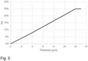
Fig. 5 depicts the results of an example. -
- 1
- substrate
- 2
- first silicon germanium buffer layer grown with a first growth rate
- 3
- second silicon germanium buffer layer grown with a second growth rate
- The growth rate influence on TDD in a first stage of buffer growth (nucleation phase) has been examined in a first set of experiments. The sample configuration used in the first set of experiments is depicted in
Fig. 1 . - A graded
SiGe buffer layer 2 to a final concentration of 8% Ge was grown on a silicon single crystal wafer 1 (Fig. 1 ). The growth rate was varied from 0.05 µm/min to 0.8 µm/min and a grading rate of 4% Ge/µm has been used. The resulting TDD has been measured after defect selective etching. As shown inFig. 2 , which displays the TDD over the growth rate GR, the TDD decreases with increasing growth rate to a minimum at 0.46 µm/min. - The growth rate influence in second stage of buffer growth (grading phase) has been examined in a second set of experiments. The sample configuration used in the second set of experiments is depicted in
Fig. 3 . - On top of a first
SiGe buffer layer 2 with a Ge-concentration of 8%, a second gradedbuffer layer 3 was grown to a final concentration of 16% Ge. A grading rate of 4% Ge/µm has been used. The growth rate of thesecond layer 2 has been varied from 0.05 µm/min to 0.95 µm/min. From 0.05 µm/min to 0.23 µm/min the TDD increases, at higher growth rates the TDD stays constant. As shown inFig. 4 , the lowest TDD is realized at lower growth rates. - A full strain relaxed graded buffer layer up to a germanium content of 25% Ge has been deposited on a silicon single crystal wafer in accordance with the claimed invention (example). During the first stage of the deposition process, i.e. from the beginning of the process until a germanium content of 8 % Ge has been reached, the growth rate was 0.46 µm / min in accordance with the results of the first set of experiments and in order to generate a low base TDD within the base layer. For further grading up to the final content of 25% Ge the growth rate was 0.05 µm / min in accordance with the results of the second set of experiments. The overall grading rate was 2.1 % Ge / µm. As shown in
Fig. 5 which depicts the content of germanium in the grown buffer layer over the thickness of the grown buffer layer, the final TDD achieved was 4 × 10⁴ / cm2. The dotted line inFig. 5 represents the first stage, the solid line the second stage of the deposition process. - The sets of experiments and the example have been performed in a commercial epitaxial reactor of type EPSILON 3200 manufactured by ASM at a deposition temperature of 1050 °C and with GeCl4 and SiH2Cl2 as precursor gases.
Claims (5)
- A method for depositing a strain relaxed graded buffer layer of silicon germanium on a surface of a substrate, the surface consisting of silicon and the buffer layer having an increasing content of germanium up to a final content, the method comprisingconducting GeCl4 and SiH2Cl2 during a first and a second stage over the surface of the substrate at a deposition temperature of not less than 800 °C;growing the buffer layer with a grade rate that is less than 10 % Ge / µm; andgrowing the buffer layer with a growth rate that is not less than 0.1 µm / min during the first stage and that is less than 0.1 µm / min during the second stage.
- The method as claimed in claim 1, wherein the first stage ends not later than when 1/3 of the final content of germanium has been reached
- The method as claimed in claim 1 or claim 2, wherein the final content of germanium is not less than 2 % Ge and not more than 90 % Ge.
- The method as claimed in one of claims 1 to 3, wherein the buffer layer is deposited by chemical vapor deposition.
- The method as claimed in one of claims 1 to 4, wherein the buffer layer is grown on a silicon single crystal wafer or on a SOI wafer.
Priority Applications (7)
| Application Number | Priority Date | Filing Date | Title |
|---|---|---|---|
| EP22154292.1A EP4220686B1 (en) | 2022-01-31 | 2022-01-31 | Method for depositing a strain relaxed graded buffer layer of silicon germanium on a surface of a substrate |
| KR1020247028941A KR102871173B1 (en) | 2022-01-31 | 2022-12-14 | Method for depositing a strain-relief graded buffer layer of silicon germanium on the surface of a substrate |
| US18/833,949 US20250101576A1 (en) | 2022-01-31 | 2022-12-14 | Method for depositing a strain relaxed graded buffer layer of silicon germanium on a surface of a substrate |
| JP2024543959A JP7693955B2 (en) | 2022-01-31 | 2022-12-14 | Method for depositing a strain-relieved graded buffer layer of silicon germanium on a surface of a substrate - Patents.com |
| CN202280090452.6A CN118633141A (en) | 2022-01-31 | 2022-12-14 | Method for depositing a strain-relaxed graded buffer layer of silicon germanium on a surface of a substrate |
| PCT/EP2022/085871 WO2023143804A1 (en) | 2022-01-31 | 2022-12-14 | Method for depositing a strain relaxed graded buffer layer of silicon germanium on a surface of a substrate |
| TW112102157A TWI890021B (en) | 2022-01-31 | 2023-01-18 | Method for depositing a strain relaxed graded buffer layer of silicon germanium on a surface of a substrate |
Applications Claiming Priority (1)
| Application Number | Priority Date | Filing Date | Title |
|---|---|---|---|
| EP22154292.1A EP4220686B1 (en) | 2022-01-31 | 2022-01-31 | Method for depositing a strain relaxed graded buffer layer of silicon germanium on a surface of a substrate |
Publications (2)
| Publication Number | Publication Date |
|---|---|
| EP4220686A1 EP4220686A1 (en) | 2023-08-02 |
| EP4220686B1 true EP4220686B1 (en) | 2024-07-10 |
Family
ID=80119675
Family Applications (1)
| Application Number | Title | Priority Date | Filing Date |
|---|---|---|---|
| EP22154292.1A Active EP4220686B1 (en) | 2022-01-31 | 2022-01-31 | Method for depositing a strain relaxed graded buffer layer of silicon germanium on a surface of a substrate |
Country Status (7)
| Country | Link |
|---|---|
| US (1) | US20250101576A1 (en) |
| EP (1) | EP4220686B1 (en) |
| JP (1) | JP7693955B2 (en) |
| KR (1) | KR102871173B1 (en) |
| CN (1) | CN118633141A (en) |
| TW (1) | TWI890021B (en) |
| WO (1) | WO2023143804A1 (en) |
Family Cites Families (14)
| Publication number | Priority date | Publication date | Assignee | Title |
|---|---|---|---|---|
| DE69827824T3 (en) | 1997-06-24 | 2009-09-03 | Massachusetts Institute Of Technology, Cambridge | CONTROL OF SEVENING DENSITY THROUGH THE USE OF GRADIENT LAYERS AND BY PLANARIZATION |
| US7041170B2 (en) * | 1999-09-20 | 2006-05-09 | Amberwave Systems Corporation | Method of producing high quality relaxed silicon germanium layers |
| EP1214735A1 (en) | 1999-09-20 | 2002-06-19 | Amberwave Systems Corporation | Method of producing relaxed silicon germanium layers |
| US6649492B2 (en) | 2002-02-11 | 2003-11-18 | International Business Machines Corporation | Strained Si based layer made by UHV-CVD, and devices therein |
| WO2003079415A2 (en) * | 2002-03-14 | 2003-09-25 | Amberwave Systems Corporation | Methods for fabricating strained layers on semiconductor substrates |
| EP1588406B1 (en) | 2003-01-27 | 2019-07-10 | Taiwan Semiconductor Manufacturing Company, Ltd. | Semiconductor structures with structural homogeneity |
| TWI336102B (en) | 2003-03-13 | 2011-01-11 | Asm Inc | Epitaxial semiconductor deposition methods and structures |
| DE102005000826A1 (en) * | 2005-01-05 | 2006-07-20 | Siltronic Ag | Semiconductor wafer with silicon-germanium layer and method for its production |
| US7902046B2 (en) | 2005-09-19 | 2011-03-08 | The Board Of Trustees Of The Leland Stanford Junior University | Thin buffer layers for SiGe growth on mismatched substrates |
| JP2007194336A (en) | 2006-01-18 | 2007-08-02 | Sumco Corp | Manufacturing method of semiconductor wafer |
| EP2104135B1 (en) * | 2008-03-20 | 2013-06-12 | Siltronic AG | A semiconductor wafer with a heteroepitaxial layer and a method for producing the wafer |
| US9343303B2 (en) * | 2014-03-20 | 2016-05-17 | Samsung Electronics Co., Ltd. | Methods of forming low-defect strain-relaxed layers on lattice-mismatched substrates and related semiconductor structures and devices |
| US9691860B2 (en) | 2014-05-02 | 2017-06-27 | Samsung Electronics Co., Ltd. | Methods of forming defect-free SRB onto lattice-mismatched substrates and defect-free fins on insulators |
| FR3061803B1 (en) * | 2017-01-11 | 2019-08-16 | Soitec | FRONT-SIDE TYPE IMAGE SENSOR SUBSTRATE AND METHOD OF MANUFACTURING SUCH A SUBSTRATE |
-
2022
- 2022-01-31 EP EP22154292.1A patent/EP4220686B1/en active Active
- 2022-12-14 CN CN202280090452.6A patent/CN118633141A/en active Pending
- 2022-12-14 JP JP2024543959A patent/JP7693955B2/en active Active
- 2022-12-14 KR KR1020247028941A patent/KR102871173B1/en active Active
- 2022-12-14 WO PCT/EP2022/085871 patent/WO2023143804A1/en not_active Ceased
- 2022-12-14 US US18/833,949 patent/US20250101576A1/en active Pending
-
2023
- 2023-01-18 TW TW112102157A patent/TWI890021B/en active
Also Published As
| Publication number | Publication date |
|---|---|
| KR20240140956A (en) | 2024-09-24 |
| WO2023143804A1 (en) | 2023-08-03 |
| TWI890021B (en) | 2025-07-11 |
| TW202332814A (en) | 2023-08-16 |
| KR102871173B1 (en) | 2025-10-14 |
| US20250101576A1 (en) | 2025-03-27 |
| EP4220686A1 (en) | 2023-08-02 |
| JP7693955B2 (en) | 2025-06-17 |
| JP2025503787A (en) | 2025-02-04 |
| CN118633141A (en) | 2024-09-10 |
Similar Documents
| Publication | Publication Date | Title |
|---|---|---|
| JP4850960B2 (en) | Epitaxial silicon carbide single crystal substrate manufacturing method | |
| US7666799B2 (en) | Epitaxial growth of relaxed silicon germanium layers | |
| KR101037636B1 (en) | Semiconductor wafers with heteroepitaxial layers and methods of manufacturing semiconductor wafers | |
| EP2016205B1 (en) | SEMICONDUCTOR STRAIN RELAXED SiGe BUFFER STRUCTURES | |
| Atzmon et al. | Chemical vapor deposition of heteroepitaxial Si1− x− y Ge x C y films on (100) Si substrates | |
| KR101971597B1 (en) | Wafer and method of fabrication thin film | |
| EP2064729A2 (en) | Thick nitride semiconductor structures with interlayer structures and methods of fabricating thick nitride semiconductor structures | |
| WO2001022482A9 (en) | Method of producing relaxed silicon germanium layers | |
| US20100019278A1 (en) | Multilayer Structure Comprising A Substrate and A Layer Of Silicon and Germanium Deposited Heteroepitaxially Thereon, and A Process For Producing It | |
| Kissinger et al. | Stepwise equilibrated graded Ge x Si1− x buffer with very low threading dislocation density on Si (001) | |
| JP2023045163A (en) | Method for manufacturing heteroepitaxial wafer | |
| CA1337170C (en) | Method for forming crystalline deposited film | |
| EP4220686A1 (en) | Method for depositing a strain relaxed graded buffer layer of silicon germanium on a surface of a substrate | |
| JP4158607B2 (en) | Manufacturing method of semiconductor substrate | |
| JP7218832B1 (en) | Manufacturing method of heteroepitaxial wafer | |
| JP2006319310A (en) | Laminated layer structure and method for forming the same | |
| US8115195B2 (en) | Semiconductor wafer with a heteroepitaxial layer and a method for producing the wafer | |
| JP2004349522A (en) | Semiconductor substrate manufacturing method | |
| WO2023058355A1 (en) | Method for forming heteroepitaxial film |
Legal Events
| Date | Code | Title | Description |
|---|---|---|---|
| PUAI | Public reference made under article 153(3) epc to a published international application that has entered the european phase |
Free format text: ORIGINAL CODE: 0009012 |
|
| STAA | Information on the status of an ep patent application or granted ep patent |
Free format text: STATUS: THE APPLICATION HAS BEEN PUBLISHED |
|
| AK | Designated contracting states |
Kind code of ref document: A1 Designated state(s): AL AT BE BG CH CY CZ DE DK EE ES FI FR GB GR HR HU IE IS IT LI LT LU LV MC MK MT NL NO PL PT RO RS SE SI SK SM TR |
|
| STAA | Information on the status of an ep patent application or granted ep patent |
Free format text: STATUS: REQUEST FOR EXAMINATION WAS MADE |
|
| 17P | Request for examination filed |
Effective date: 20230915 |
|
| RBV | Designated contracting states (corrected) |
Designated state(s): AL AT BE BG CH CY CZ DE DK EE ES FI FR GB GR HR HU IE IS IT LI LT LU LV MC MK MT NL NO PL PT RO RS SE SI SK SM TR |
|
| GRAP | Despatch of communication of intention to grant a patent |
Free format text: ORIGINAL CODE: EPIDOSNIGR1 |
|
| STAA | Information on the status of an ep patent application or granted ep patent |
Free format text: STATUS: GRANT OF PATENT IS INTENDED |
|
| RIC1 | Information provided on ipc code assigned before grant |
Ipc: H01L 21/20 20060101AFI20240201BHEP |
|
| INTG | Intention to grant announced |
Effective date: 20240220 |
|
| GRAS | Grant fee paid |
Free format text: ORIGINAL CODE: EPIDOSNIGR3 |
|
| GRAA | (expected) grant |
Free format text: ORIGINAL CODE: 0009210 |
|
| STAA | Information on the status of an ep patent application or granted ep patent |
Free format text: STATUS: THE PATENT HAS BEEN GRANTED |
|
| AK | Designated contracting states |
Kind code of ref document: B1 Designated state(s): AL AT BE BG CH CY CZ DE DK EE ES FI FR GB GR HR HU IE IS IT LI LT LU LV MC MK MT NL NO PL PT RO RS SE SI SK SM TR |
|
| REG | Reference to a national code |
Ref country code: CH Ref legal event code: EP |
|
| REG | Reference to a national code |
Ref country code: DE Ref legal event code: R096 Ref document number: 602022004380 Country of ref document: DE |
|
| REG | Reference to a national code |
Ref country code: LT Ref legal event code: MG9D |
|
| REG | Reference to a national code |
Ref country code: NL Ref legal event code: MP Effective date: 20240710 |
|
| PG25 | Lapsed in a contracting state [announced via postgrant information from national office to epo] |
Ref country code: PT Free format text: LAPSE BECAUSE OF FAILURE TO SUBMIT A TRANSLATION OF THE DESCRIPTION OR TO PAY THE FEE WITHIN THE PRESCRIBED TIME-LIMIT Effective date: 20241111 |
|
| REG | Reference to a national code |
Ref country code: AT Ref legal event code: MK05 Ref document number: 1702814 Country of ref document: AT Kind code of ref document: T Effective date: 20240710 |
|
| PG25 | Lapsed in a contracting state [announced via postgrant information from national office to epo] |
Ref country code: NL Free format text: LAPSE BECAUSE OF FAILURE TO SUBMIT A TRANSLATION OF THE DESCRIPTION OR TO PAY THE FEE WITHIN THE PRESCRIBED TIME-LIMIT Effective date: 20240710 |
|
| PG25 | Lapsed in a contracting state [announced via postgrant information from national office to epo] |
Ref country code: PT Free format text: LAPSE BECAUSE OF FAILURE TO SUBMIT A TRANSLATION OF THE DESCRIPTION OR TO PAY THE FEE WITHIN THE PRESCRIBED TIME-LIMIT Effective date: 20241111 Ref country code: NL Free format text: LAPSE BECAUSE OF FAILURE TO SUBMIT A TRANSLATION OF THE DESCRIPTION OR TO PAY THE FEE WITHIN THE PRESCRIBED TIME-LIMIT Effective date: 20240710 |
|
| PG25 | Lapsed in a contracting state [announced via postgrant information from national office to epo] |
Ref country code: NO Free format text: LAPSE BECAUSE OF FAILURE TO SUBMIT A TRANSLATION OF THE DESCRIPTION OR TO PAY THE FEE WITHIN THE PRESCRIBED TIME-LIMIT Effective date: 20241010 |
|
| PG25 | Lapsed in a contracting state [announced via postgrant information from national office to epo] |
Ref country code: GR Free format text: LAPSE BECAUSE OF FAILURE TO SUBMIT A TRANSLATION OF THE DESCRIPTION OR TO PAY THE FEE WITHIN THE PRESCRIBED TIME-LIMIT Effective date: 20241011 Ref country code: FI Free format text: LAPSE BECAUSE OF FAILURE TO SUBMIT A TRANSLATION OF THE DESCRIPTION OR TO PAY THE FEE WITHIN THE PRESCRIBED TIME-LIMIT Effective date: 20240710 Ref country code: PL Free format text: LAPSE BECAUSE OF FAILURE TO SUBMIT A TRANSLATION OF THE DESCRIPTION OR TO PAY THE FEE WITHIN THE PRESCRIBED TIME-LIMIT Effective date: 20240710 |
|
| PG25 | Lapsed in a contracting state [announced via postgrant information from national office to epo] |
Ref country code: BG Free format text: LAPSE BECAUSE OF FAILURE TO SUBMIT A TRANSLATION OF THE DESCRIPTION OR TO PAY THE FEE WITHIN THE PRESCRIBED TIME-LIMIT Effective date: 20240710 |
|
| PG25 | Lapsed in a contracting state [announced via postgrant information from national office to epo] |
Ref country code: LV Free format text: LAPSE BECAUSE OF FAILURE TO SUBMIT A TRANSLATION OF THE DESCRIPTION OR TO PAY THE FEE WITHIN THE PRESCRIBED TIME-LIMIT Effective date: 20240710 |
|
| PG25 | Lapsed in a contracting state [announced via postgrant information from national office to epo] |
Ref country code: AT Free format text: LAPSE BECAUSE OF FAILURE TO SUBMIT A TRANSLATION OF THE DESCRIPTION OR TO PAY THE FEE WITHIN THE PRESCRIBED TIME-LIMIT Effective date: 20240710 Ref country code: IS Free format text: LAPSE BECAUSE OF FAILURE TO SUBMIT A TRANSLATION OF THE DESCRIPTION OR TO PAY THE FEE WITHIN THE PRESCRIBED TIME-LIMIT Effective date: 20241110 |
|
| PG25 | Lapsed in a contracting state [announced via postgrant information from national office to epo] |
Ref country code: HR Free format text: LAPSE BECAUSE OF FAILURE TO SUBMIT A TRANSLATION OF THE DESCRIPTION OR TO PAY THE FEE WITHIN THE PRESCRIBED TIME-LIMIT Effective date: 20240710 |
|
| PG25 | Lapsed in a contracting state [announced via postgrant information from national office to epo] |
Ref country code: ES Free format text: LAPSE BECAUSE OF FAILURE TO SUBMIT A TRANSLATION OF THE DESCRIPTION OR TO PAY THE FEE WITHIN THE PRESCRIBED TIME-LIMIT Effective date: 20240710 Ref country code: RS Free format text: LAPSE BECAUSE OF FAILURE TO SUBMIT A TRANSLATION OF THE DESCRIPTION OR TO PAY THE FEE WITHIN THE PRESCRIBED TIME-LIMIT Effective date: 20241010 |
|
| PG25 | Lapsed in a contracting state [announced via postgrant information from national office to epo] |
Ref country code: RS Free format text: LAPSE BECAUSE OF FAILURE TO SUBMIT A TRANSLATION OF THE DESCRIPTION OR TO PAY THE FEE WITHIN THE PRESCRIBED TIME-LIMIT Effective date: 20241010 Ref country code: PL Free format text: LAPSE BECAUSE OF FAILURE TO SUBMIT A TRANSLATION OF THE DESCRIPTION OR TO PAY THE FEE WITHIN THE PRESCRIBED TIME-LIMIT Effective date: 20240710 Ref country code: NO Free format text: LAPSE BECAUSE OF FAILURE TO SUBMIT A TRANSLATION OF THE DESCRIPTION OR TO PAY THE FEE WITHIN THE PRESCRIBED TIME-LIMIT Effective date: 20241010 Ref country code: LV Free format text: LAPSE BECAUSE OF FAILURE TO SUBMIT A TRANSLATION OF THE DESCRIPTION OR TO PAY THE FEE WITHIN THE PRESCRIBED TIME-LIMIT Effective date: 20240710 Ref country code: IS Free format text: LAPSE BECAUSE OF FAILURE TO SUBMIT A TRANSLATION OF THE DESCRIPTION OR TO PAY THE FEE WITHIN THE PRESCRIBED TIME-LIMIT Effective date: 20241110 Ref country code: HR Free format text: LAPSE BECAUSE OF FAILURE TO SUBMIT A TRANSLATION OF THE DESCRIPTION OR TO PAY THE FEE WITHIN THE PRESCRIBED TIME-LIMIT Effective date: 20240710 Ref country code: GR Free format text: LAPSE BECAUSE OF FAILURE TO SUBMIT A TRANSLATION OF THE DESCRIPTION OR TO PAY THE FEE WITHIN THE PRESCRIBED TIME-LIMIT Effective date: 20241011 Ref country code: FI Free format text: LAPSE BECAUSE OF FAILURE TO SUBMIT A TRANSLATION OF THE DESCRIPTION OR TO PAY THE FEE WITHIN THE PRESCRIBED TIME-LIMIT Effective date: 20240710 Ref country code: ES Free format text: LAPSE BECAUSE OF FAILURE TO SUBMIT A TRANSLATION OF THE DESCRIPTION OR TO PAY THE FEE WITHIN THE PRESCRIBED TIME-LIMIT Effective date: 20240710 Ref country code: BG Free format text: LAPSE BECAUSE OF FAILURE TO SUBMIT A TRANSLATION OF THE DESCRIPTION OR TO PAY THE FEE WITHIN THE PRESCRIBED TIME-LIMIT Effective date: 20240710 Ref country code: AT Free format text: LAPSE BECAUSE OF FAILURE TO SUBMIT A TRANSLATION OF THE DESCRIPTION OR TO PAY THE FEE WITHIN THE PRESCRIBED TIME-LIMIT Effective date: 20240710 |
|
| REG | Reference to a national code |
Ref country code: DE Ref legal event code: R097 Ref document number: 602022004380 Country of ref document: DE |
|
| PG25 | Lapsed in a contracting state [announced via postgrant information from national office to epo] |
Ref country code: RO Free format text: LAPSE BECAUSE OF FAILURE TO SUBMIT A TRANSLATION OF THE DESCRIPTION OR TO PAY THE FEE WITHIN THE PRESCRIBED TIME-LIMIT Effective date: 20240710 Ref country code: DK Free format text: LAPSE BECAUSE OF FAILURE TO SUBMIT A TRANSLATION OF THE DESCRIPTION OR TO PAY THE FEE WITHIN THE PRESCRIBED TIME-LIMIT Effective date: 20240710 Ref country code: SM Free format text: LAPSE BECAUSE OF FAILURE TO SUBMIT A TRANSLATION OF THE DESCRIPTION OR TO PAY THE FEE WITHIN THE PRESCRIBED TIME-LIMIT Effective date: 20240710 |
|
| PG25 | Lapsed in a contracting state [announced via postgrant information from national office to epo] |
Ref country code: EE Free format text: LAPSE BECAUSE OF FAILURE TO SUBMIT A TRANSLATION OF THE DESCRIPTION OR TO PAY THE FEE WITHIN THE PRESCRIBED TIME-LIMIT Effective date: 20240710 |
|
| PG25 | Lapsed in a contracting state [announced via postgrant information from national office to epo] |
Ref country code: CZ Free format text: LAPSE BECAUSE OF FAILURE TO SUBMIT A TRANSLATION OF THE DESCRIPTION OR TO PAY THE FEE WITHIN THE PRESCRIBED TIME-LIMIT Effective date: 20240710 |
|
| PG25 | Lapsed in a contracting state [announced via postgrant information from national office to epo] |
Ref country code: SK Free format text: LAPSE BECAUSE OF FAILURE TO SUBMIT A TRANSLATION OF THE DESCRIPTION OR TO PAY THE FEE WITHIN THE PRESCRIBED TIME-LIMIT Effective date: 20240710 |
|
| PLBE | No opposition filed within time limit |
Free format text: ORIGINAL CODE: 0009261 |
|
| STAA | Information on the status of an ep patent application or granted ep patent |
Free format text: STATUS: NO OPPOSITION FILED WITHIN TIME LIMIT |
|
| 26N | No opposition filed |
Effective date: 20250411 |
|
| REG | Reference to a national code |
Ref country code: CH Ref legal event code: PL |
|
| PG25 | Lapsed in a contracting state [announced via postgrant information from national office to epo] |
Ref country code: SE Free format text: LAPSE BECAUSE OF FAILURE TO SUBMIT A TRANSLATION OF THE DESCRIPTION OR TO PAY THE FEE WITHIN THE PRESCRIBED TIME-LIMIT Effective date: 20240710 |
|
| PG25 | Lapsed in a contracting state [announced via postgrant information from national office to epo] |
Ref country code: LU Free format text: LAPSE BECAUSE OF NON-PAYMENT OF DUE FEES Effective date: 20250131 Ref country code: MC Free format text: LAPSE BECAUSE OF FAILURE TO SUBMIT A TRANSLATION OF THE DESCRIPTION OR TO PAY THE FEE WITHIN THE PRESCRIBED TIME-LIMIT Effective date: 20240710 |
|
| PG25 | Lapsed in a contracting state [announced via postgrant information from national office to epo] |
Ref country code: BE Free format text: LAPSE BECAUSE OF NON-PAYMENT OF DUE FEES Effective date: 20250131 |
|
| PG25 | Lapsed in a contracting state [announced via postgrant information from national office to epo] |
Ref country code: CH Free format text: LAPSE BECAUSE OF NON-PAYMENT OF DUE FEES Effective date: 20250131 |
|
| REG | Reference to a national code |
Ref country code: BE Ref legal event code: MM Effective date: 20250131 |
|
| REG | Reference to a national code |
Ref country code: DE Ref legal event code: R079 Ref document number: 602022004380 Country of ref document: DE Free format text: PREVIOUS MAIN CLASS: H01L0021200000 Ipc: H10P0014200000 |
|
| PGFP | Annual fee paid to national office [announced via postgrant information from national office to epo] |
Ref country code: IE Payment date: 20260120 Year of fee payment: 5 Ref country code: DE Payment date: 20260127 Year of fee payment: 5 |
|
| PGFP | Annual fee paid to national office [announced via postgrant information from national office to epo] |
Ref country code: IT Payment date: 20260123 Year of fee payment: 5 |
|
| PGFP | Annual fee paid to national office [announced via postgrant information from national office to epo] |
Ref country code: FR Payment date: 20260126 Year of fee payment: 5 |