EP4216271A1 - Semiconductor package including a chip-substrate composite semiconductor device - Google Patents
Semiconductor package including a chip-substrate composite semiconductor device Download PDFInfo
- Publication number
- EP4216271A1 EP4216271A1 EP22152677.5A EP22152677A EP4216271A1 EP 4216271 A1 EP4216271 A1 EP 4216271A1 EP 22152677 A EP22152677 A EP 22152677A EP 4216271 A1 EP4216271 A1 EP 4216271A1
- Authority
- EP
- European Patent Office
- Prior art keywords
- high voltage
- inorganic substrate
- dielectric inorganic
- semiconductor package
- metal
- Prior art date
- Legal status (The legal status is an assumption and is not a legal conclusion. Google has not performed a legal analysis and makes no representation as to the accuracy of the status listed.)
- Pending
Links
Images




Classifications
-
- H—ELECTRICITY
- H10—SEMICONDUCTOR DEVICES; ELECTRIC SOLID-STATE DEVICES NOT OTHERWISE PROVIDED FOR
- H10W—GENERIC PACKAGES, INTERCONNECTIONS, CONNECTORS OR OTHER CONSTRUCTIONAL DETAILS OF DEVICES COVERED BY CLASS H10
- H10W70/00—Package substrates; Interposers; Redistribution layers [RDL]
- H10W70/40—Leadframes
-
- H—ELECTRICITY
- H10—SEMICONDUCTOR DEVICES; ELECTRIC SOLID-STATE DEVICES NOT OTHERWISE PROVIDED FOR
- H10W—GENERIC PACKAGES, INTERCONNECTIONS, CONNECTORS OR OTHER CONSTRUCTIONAL DETAILS OF DEVICES COVERED BY CLASS H10
- H10W70/00—Package substrates; Interposers; Redistribution layers [RDL]
- H10W70/40—Leadframes
- H10W70/481—Leadframes for devices being provided for in groups H10D8/00 - H10D48/00
-
- H—ELECTRICITY
- H10—SEMICONDUCTOR DEVICES; ELECTRIC SOLID-STATE DEVICES NOT OTHERWISE PROVIDED FOR
- H10W—GENERIC PACKAGES, INTERCONNECTIONS, CONNECTORS OR OTHER CONSTRUCTIONAL DETAILS OF DEVICES COVERED BY CLASS H10
- H10W70/00—Package substrates; Interposers; Redistribution layers [RDL]
- H10W70/60—Insulating or insulated package substrates; Interposers; Redistribution layers
- H10W70/67—Insulating or insulated package substrates; Interposers; Redistribution layers characterised by their insulating layers or insulating parts
- H10W70/68—Shapes or dispositions thereof
- H10W70/6875—Shapes or dispositions thereof being on a metallic substrate, e.g. insulated metal substrates [IMS]
-
- H—ELECTRICITY
- H05—ELECTRIC TECHNIQUES NOT OTHERWISE PROVIDED FOR
- H05K—PRINTED CIRCUITS; CASINGS OR CONSTRUCTIONAL DETAILS OF ELECTRIC APPARATUS; MANUFACTURE OF ASSEMBLAGES OF ELECTRICAL COMPONENTS
- H05K1/00—Printed circuits
- H05K1/18—Printed circuits structurally associated with non-printed electric components
-
- H—ELECTRICITY
- H05—ELECTRIC TECHNIQUES NOT OTHERWISE PROVIDED FOR
- H05K—PRINTED CIRCUITS; CASINGS OR CONSTRUCTIONAL DETAILS OF ELECTRIC APPARATUS; MANUFACTURE OF ASSEMBLAGES OF ELECTRICAL COMPONENTS
- H05K1/00—Printed circuits
- H05K1/18—Printed circuits structurally associated with non-printed electric components
- H05K1/182—Printed circuits structurally associated with non-printed electric components associated with components mounted in printed circuit boards [PCB], e.g. insert-mounted components [IMC]
- H05K1/185—Printed circuits structurally associated with non-printed electric components associated with components mounted in printed circuit boards [PCB], e.g. insert-mounted components [IMC] associated with components encapsulated in the insulating substrate of the PCBs; associated with components incorporated in internal layers of multilayer circuit boards
-
- H—ELECTRICITY
- H10—SEMICONDUCTOR DEVICES; ELECTRIC SOLID-STATE DEVICES NOT OTHERWISE PROVIDED FOR
- H10W—GENERIC PACKAGES, INTERCONNECTIONS, CONNECTORS OR OTHER CONSTRUCTIONAL DETAILS OF DEVICES COVERED BY CLASS H10
- H10W20/00—Interconnections in chips, wafers or substrates
- H10W20/01—Manufacture or treatment
- H10W20/071—Manufacture or treatment of dielectric parts thereof
- H10W20/081—Manufacture or treatment of dielectric parts thereof by forming openings in the dielectric parts
-
- H—ELECTRICITY
- H10—SEMICONDUCTOR DEVICES; ELECTRIC SOLID-STATE DEVICES NOT OTHERWISE PROVIDED FOR
- H10W—GENERIC PACKAGES, INTERCONNECTIONS, CONNECTORS OR OTHER CONSTRUCTIONAL DETAILS OF DEVICES COVERED BY CLASS H10
- H10W20/00—Interconnections in chips, wafers or substrates
- H10W20/40—Interconnections external to wafers or substrates, e.g. back-end-of-line [BEOL] metallisations or vias connecting to gate electrodes
- H10W20/41—Interconnections external to wafers or substrates, e.g. back-end-of-line [BEOL] metallisations or vias connecting to gate electrodes characterised by their conductive parts
- H10W20/43—Layouts of interconnections
-
- H—ELECTRICITY
- H10—SEMICONDUCTOR DEVICES; ELECTRIC SOLID-STATE DEVICES NOT OTHERWISE PROVIDED FOR
- H10W—GENERIC PACKAGES, INTERCONNECTIONS, CONNECTORS OR OTHER CONSTRUCTIONAL DETAILS OF DEVICES COVERED BY CLASS H10
- H10W20/00—Interconnections in chips, wafers or substrates
- H10W20/40—Interconnections external to wafers or substrates, e.g. back-end-of-line [BEOL] metallisations or vias connecting to gate electrodes
- H10W20/482—Interconnections external to wafers or substrates, e.g. back-end-of-line [BEOL] metallisations or vias connecting to gate electrodes for individual devices provided for in groups H10D8/00 - H10D48/00, e.g. for power transistors
- H10W20/484—Interconnections having extended contours, e.g. pads having mesh shape or interconnections comprising connected parallel stripes
-
- H—ELECTRICITY
- H10—SEMICONDUCTOR DEVICES; ELECTRIC SOLID-STATE DEVICES NOT OTHERWISE PROVIDED FOR
- H10W—GENERIC PACKAGES, INTERCONNECTIONS, CONNECTORS OR OTHER CONSTRUCTIONAL DETAILS OF DEVICES COVERED BY CLASS H10
- H10W70/00—Package substrates; Interposers; Redistribution layers [RDL]
- H10W70/01—Manufacture or treatment
- H10W70/05—Manufacture or treatment of insulating or insulated package substrates, or of interposers, or of redistribution layers
-
- H—ELECTRICITY
- H10—SEMICONDUCTOR DEVICES; ELECTRIC SOLID-STATE DEVICES NOT OTHERWISE PROVIDED FOR
- H10W—GENERIC PACKAGES, INTERCONNECTIONS, CONNECTORS OR OTHER CONSTRUCTIONAL DETAILS OF DEVICES COVERED BY CLASS H10
- H10W70/00—Package substrates; Interposers; Redistribution layers [RDL]
- H10W70/01—Manufacture or treatment
- H10W70/05—Manufacture or treatment of insulating or insulated package substrates, or of interposers, or of redistribution layers
- H10W70/095—Manufacture or treatment of insulating or insulated package substrates, or of interposers, or of redistribution layers of vias therein
-
- H—ELECTRICITY
- H10—SEMICONDUCTOR DEVICES; ELECTRIC SOLID-STATE DEVICES NOT OTHERWISE PROVIDED FOR
- H10W—GENERIC PACKAGES, INTERCONNECTIONS, CONNECTORS OR OTHER CONSTRUCTIONAL DETAILS OF DEVICES COVERED BY CLASS H10
- H10W70/00—Package substrates; Interposers; Redistribution layers [RDL]
- H10W70/40—Leadframes
- H10W70/421—Shapes or dispositions
-
- H—ELECTRICITY
- H10—SEMICONDUCTOR DEVICES; ELECTRIC SOLID-STATE DEVICES NOT OTHERWISE PROVIDED FOR
- H10W—GENERIC PACKAGES, INTERCONNECTIONS, CONNECTORS OR OTHER CONSTRUCTIONAL DETAILS OF DEVICES COVERED BY CLASS H10
- H10W70/00—Package substrates; Interposers; Redistribution layers [RDL]
- H10W70/40—Leadframes
- H10W70/479—Leadframes on or in insulating or insulated package substrates, interposers, or redistribution layers
-
- H—ELECTRICITY
- H10—SEMICONDUCTOR DEVICES; ELECTRIC SOLID-STATE DEVICES NOT OTHERWISE PROVIDED FOR
- H10W—GENERIC PACKAGES, INTERCONNECTIONS, CONNECTORS OR OTHER CONSTRUCTIONAL DETAILS OF DEVICES COVERED BY CLASS H10
- H10W70/00—Package substrates; Interposers; Redistribution layers [RDL]
- H10W70/60—Insulating or insulated package substrates; Interposers; Redistribution layers
- H10W70/62—Insulating or insulated package substrates; Interposers; Redistribution layers characterised by their interconnections
- H10W70/63—Vias, e.g. via plugs
- H10W70/635—Through-vias
-
- H—ELECTRICITY
- H10—SEMICONDUCTOR DEVICES; ELECTRIC SOLID-STATE DEVICES NOT OTHERWISE PROVIDED FOR
- H10W—GENERIC PACKAGES, INTERCONNECTIONS, CONNECTORS OR OTHER CONSTRUCTIONAL DETAILS OF DEVICES COVERED BY CLASS H10
- H10W70/00—Package substrates; Interposers; Redistribution layers [RDL]
- H10W70/60—Insulating or insulated package substrates; Interposers; Redistribution layers
- H10W70/62—Insulating or insulated package substrates; Interposers; Redistribution layers characterised by their interconnections
- H10W70/65—Shapes or dispositions of interconnections
-
- H—ELECTRICITY
- H10—SEMICONDUCTOR DEVICES; ELECTRIC SOLID-STATE DEVICES NOT OTHERWISE PROVIDED FOR
- H10W—GENERIC PACKAGES, INTERCONNECTIONS, CONNECTORS OR OTHER CONSTRUCTIONAL DETAILS OF DEVICES COVERED BY CLASS H10
- H10W70/00—Package substrates; Interposers; Redistribution layers [RDL]
- H10W70/60—Insulating or insulated package substrates; Interposers; Redistribution layers
- H10W70/67—Insulating or insulated package substrates; Interposers; Redistribution layers characterised by their insulating layers or insulating parts
- H10W70/68—Shapes or dispositions thereof
- H10W70/685—Shapes or dispositions thereof comprising multiple insulating layers
-
- H—ELECTRICITY
- H10—SEMICONDUCTOR DEVICES; ELECTRIC SOLID-STATE DEVICES NOT OTHERWISE PROVIDED FOR
- H10W—GENERIC PACKAGES, INTERCONNECTIONS, CONNECTORS OR OTHER CONSTRUCTIONAL DETAILS OF DEVICES COVERED BY CLASS H10
- H10W70/00—Package substrates; Interposers; Redistribution layers [RDL]
- H10W70/60—Insulating or insulated package substrates; Interposers; Redistribution layers
- H10W70/67—Insulating or insulated package substrates; Interposers; Redistribution layers characterised by their insulating layers or insulating parts
- H10W70/69—Insulating materials thereof
- H10W70/692—Ceramics or glasses
-
- H—ELECTRICITY
- H10—SEMICONDUCTOR DEVICES; ELECTRIC SOLID-STATE DEVICES NOT OTHERWISE PROVIDED FOR
- H10W—GENERIC PACKAGES, INTERCONNECTIONS, CONNECTORS OR OTHER CONSTRUCTIONAL DETAILS OF DEVICES COVERED BY CLASS H10
- H10W72/00—Interconnections or connectors in packages
-
- H—ELECTRICITY
- H10—SEMICONDUCTOR DEVICES; ELECTRIC SOLID-STATE DEVICES NOT OTHERWISE PROVIDED FOR
- H10W—GENERIC PACKAGES, INTERCONNECTIONS, CONNECTORS OR OTHER CONSTRUCTIONAL DETAILS OF DEVICES COVERED BY CLASS H10
- H10W72/00—Interconnections or connectors in packages
- H10W72/30—Die-attach connectors
- H10W72/351—Materials of die-attach connectors
- H10W72/353—Materials of die-attach connectors not comprising solid metals or solid metalloids, e.g. ceramics
-
- H—ELECTRICITY
- H10—SEMICONDUCTOR DEVICES; ELECTRIC SOLID-STATE DEVICES NOT OTHERWISE PROVIDED FOR
- H10W—GENERIC PACKAGES, INTERCONNECTIONS, CONNECTORS OR OTHER CONSTRUCTIONAL DETAILS OF DEVICES COVERED BY CLASS H10
- H10W74/00—Encapsulations, e.g. protective coatings
- H10W74/10—Encapsulations, e.g. protective coatings characterised by their shape or disposition
- H10W74/111—Encapsulations, e.g. protective coatings characterised by their shape or disposition the semiconductor body being completely enclosed
- H10W74/129—Encapsulations, e.g. protective coatings characterised by their shape or disposition the semiconductor body being completely enclosed forming a chip-scale package [CSP]
-
- H—ELECTRICITY
- H10—SEMICONDUCTOR DEVICES; ELECTRIC SOLID-STATE DEVICES NOT OTHERWISE PROVIDED FOR
- H10W—GENERIC PACKAGES, INTERCONNECTIONS, CONNECTORS OR OTHER CONSTRUCTIONAL DETAILS OF DEVICES COVERED BY CLASS H10
- H10W90/00—Package configurations
- H10W90/811—Multiple chips on leadframes
-
- H—ELECTRICITY
- H10—SEMICONDUCTOR DEVICES; ELECTRIC SOLID-STATE DEVICES NOT OTHERWISE PROVIDED FOR
- H10W—GENERIC PACKAGES, INTERCONNECTIONS, CONNECTORS OR OTHER CONSTRUCTIONAL DETAILS OF DEVICES COVERED BY CLASS H10
- H10W70/00—Package substrates; Interposers; Redistribution layers [RDL]
- H10W70/099—Connecting interconnections to insulating or insulated package substrates, interposers or redistribution layers
-
- H—ELECTRICITY
- H10—SEMICONDUCTOR DEVICES; ELECTRIC SOLID-STATE DEVICES NOT OTHERWISE PROVIDED FOR
- H10W—GENERIC PACKAGES, INTERCONNECTIONS, CONNECTORS OR OTHER CONSTRUCTIONAL DETAILS OF DEVICES COVERED BY CLASS H10
- H10W70/00—Package substrates; Interposers; Redistribution layers [RDL]
- H10W70/60—Insulating or insulated package substrates; Interposers; Redistribution layers
-
- H—ELECTRICITY
- H10—SEMICONDUCTOR DEVICES; ELECTRIC SOLID-STATE DEVICES NOT OTHERWISE PROVIDED FOR
- H10W—GENERIC PACKAGES, INTERCONNECTIONS, CONNECTORS OR OTHER CONSTRUCTIONAL DETAILS OF DEVICES COVERED BY CLASS H10
- H10W70/00—Package substrates; Interposers; Redistribution layers [RDL]
- H10W70/60—Insulating or insulated package substrates; Interposers; Redistribution layers
- H10W70/62—Insulating or insulated package substrates; Interposers; Redistribution layers characterised by their interconnections
- H10W70/65—Shapes or dispositions of interconnections
- H10W70/652—Cross-sectional shapes
- H10W70/6528—Cross-sectional shapes of the portions that connect to chips, wafers or package parts
-
- H—ELECTRICITY
- H10—SEMICONDUCTOR DEVICES; ELECTRIC SOLID-STATE DEVICES NOT OTHERWISE PROVIDED FOR
- H10W—GENERIC PACKAGES, INTERCONNECTIONS, CONNECTORS OR OTHER CONSTRUCTIONAL DETAILS OF DEVICES COVERED BY CLASS H10
- H10W72/00—Interconnections or connectors in packages
- H10W72/01—Manufacture or treatment
- H10W72/0198—Manufacture or treatment batch processes
-
- H—ELECTRICITY
- H10—SEMICONDUCTOR DEVICES; ELECTRIC SOLID-STATE DEVICES NOT OTHERWISE PROVIDED FOR
- H10W—GENERIC PACKAGES, INTERCONNECTIONS, CONNECTORS OR OTHER CONSTRUCTIONAL DETAILS OF DEVICES COVERED BY CLASS H10
- H10W72/00—Interconnections or connectors in packages
- H10W72/071—Connecting or disconnecting
- H10W72/073—Connecting or disconnecting of die-attach connectors
-
- H—ELECTRICITY
- H10—SEMICONDUCTOR DEVICES; ELECTRIC SOLID-STATE DEVICES NOT OTHERWISE PROVIDED FOR
- H10W—GENERIC PACKAGES, INTERCONNECTIONS, CONNECTORS OR OTHER CONSTRUCTIONAL DETAILS OF DEVICES COVERED BY CLASS H10
- H10W72/00—Interconnections or connectors in packages
- H10W72/071—Connecting or disconnecting
- H10W72/073—Connecting or disconnecting of die-attach connectors
- H10W72/07331—Connecting techniques
-
- H—ELECTRICITY
- H10—SEMICONDUCTOR DEVICES; ELECTRIC SOLID-STATE DEVICES NOT OTHERWISE PROVIDED FOR
- H10W—GENERIC PACKAGES, INTERCONNECTIONS, CONNECTORS OR OTHER CONSTRUCTIONAL DETAILS OF DEVICES COVERED BY CLASS H10
- H10W72/00—Interconnections or connectors in packages
- H10W72/30—Die-attach connectors
-
- H—ELECTRICITY
- H10—SEMICONDUCTOR DEVICES; ELECTRIC SOLID-STATE DEVICES NOT OTHERWISE PROVIDED FOR
- H10W—GENERIC PACKAGES, INTERCONNECTIONS, CONNECTORS OR OTHER CONSTRUCTIONAL DETAILS OF DEVICES COVERED BY CLASS H10
- H10W72/00—Interconnections or connectors in packages
- H10W72/30—Die-attach connectors
- H10W72/321—Structures or relative sizes of die-attach connectors
- H10W72/327—Multiple die-attach connectors having different sizes
-
- H—ELECTRICITY
- H10—SEMICONDUCTOR DEVICES; ELECTRIC SOLID-STATE DEVICES NOT OTHERWISE PROVIDED FOR
- H10W—GENERIC PACKAGES, INTERCONNECTIONS, CONNECTORS OR OTHER CONSTRUCTIONAL DETAILS OF DEVICES COVERED BY CLASS H10
- H10W72/00—Interconnections or connectors in packages
- H10W72/851—Dispositions of multiple connectors or interconnections
- H10W72/874—On different surfaces
-
- H—ELECTRICITY
- H10—SEMICONDUCTOR DEVICES; ELECTRIC SOLID-STATE DEVICES NOT OTHERWISE PROVIDED FOR
- H10W—GENERIC PACKAGES, INTERCONNECTIONS, CONNECTORS OR OTHER CONSTRUCTIONAL DETAILS OF DEVICES COVERED BY CLASS H10
- H10W72/00—Interconnections or connectors in packages
- H10W72/90—Bond pads, in general
- H10W72/921—Structures or relative sizes of bond pads
- H10W72/926—Multiple bond pads having different sizes
-
- H—ELECTRICITY
- H10—SEMICONDUCTOR DEVICES; ELECTRIC SOLID-STATE DEVICES NOT OTHERWISE PROVIDED FOR
- H10W—GENERIC PACKAGES, INTERCONNECTIONS, CONNECTORS OR OTHER CONSTRUCTIONAL DETAILS OF DEVICES COVERED BY CLASS H10
- H10W72/00—Interconnections or connectors in packages
- H10W72/90—Bond pads, in general
- H10W72/941—Dispositions of bond pads
- H10W72/9413—Dispositions of bond pads on encapsulations
-
- H—ELECTRICITY
- H10—SEMICONDUCTOR DEVICES; ELECTRIC SOLID-STATE DEVICES NOT OTHERWISE PROVIDED FOR
- H10W—GENERIC PACKAGES, INTERCONNECTIONS, CONNECTORS OR OTHER CONSTRUCTIONAL DETAILS OF DEVICES COVERED BY CLASS H10
- H10W72/00—Interconnections or connectors in packages
- H10W72/90—Bond pads, in general
- H10W72/941—Dispositions of bond pads
- H10W72/944—Dispositions of multiple bond pads
-
- H—ELECTRICITY
- H10—SEMICONDUCTOR DEVICES; ELECTRIC SOLID-STATE DEVICES NOT OTHERWISE PROVIDED FOR
- H10W—GENERIC PACKAGES, INTERCONNECTIONS, CONNECTORS OR OTHER CONSTRUCTIONAL DETAILS OF DEVICES COVERED BY CLASS H10
- H10W80/00—Direct bonding of chips, wafers or substrates
- H10W80/301—Bonding techniques, e.g. hybrid bonding
- H10W80/312—Bonding techniques, e.g. hybrid bonding characterised by the direct bonding of electrically conductive pads
-
- H—ELECTRICITY
- H10—SEMICONDUCTOR DEVICES; ELECTRIC SOLID-STATE DEVICES NOT OTHERWISE PROVIDED FOR
- H10W—GENERIC PACKAGES, INTERCONNECTIONS, CONNECTORS OR OTHER CONSTRUCTIONAL DETAILS OF DEVICES COVERED BY CLASS H10
- H10W90/00—Package configurations
- H10W90/701—Package configurations characterised by the relative positions of pads or connectors relative to package parts
- H10W90/731—Package configurations characterised by the relative positions of pads or connectors relative to package parts of die-attach connectors
- H10W90/734—Package configurations characterised by the relative positions of pads or connectors relative to package parts of die-attach connectors between a chip and a stacked insulating package substrate, interposer or RDL
-
- H—ELECTRICITY
- H10—SEMICONDUCTOR DEVICES; ELECTRIC SOLID-STATE DEVICES NOT OTHERWISE PROVIDED FOR
- H10W—GENERIC PACKAGES, INTERCONNECTIONS, CONNECTORS OR OTHER CONSTRUCTIONAL DETAILS OF DEVICES COVERED BY CLASS H10
- H10W90/00—Package configurations
- H10W90/701—Package configurations characterised by the relative positions of pads or connectors relative to package parts
- H10W90/731—Package configurations characterised by the relative positions of pads or connectors relative to package parts of die-attach connectors
- H10W90/736—Package configurations characterised by the relative positions of pads or connectors relative to package parts of die-attach connectors between a chip and a stacked lead frame, conducting package substrate or heat sink
-
- H—ELECTRICITY
- H10—SEMICONDUCTOR DEVICES; ELECTRIC SOLID-STATE DEVICES NOT OTHERWISE PROVIDED FOR
- H10W—GENERIC PACKAGES, INTERCONNECTIONS, CONNECTORS OR OTHER CONSTRUCTIONAL DETAILS OF DEVICES COVERED BY CLASS H10
- H10W90/00—Package configurations
- H10W90/701—Package configurations characterised by the relative positions of pads or connectors relative to package parts
- H10W90/791—Package configurations characterised by the relative positions of pads or connectors relative to package parts of direct-bonded pads
- H10W90/794—Package configurations characterised by the relative positions of pads or connectors relative to package parts of direct-bonded pads between a chip and a stacked insulating package substrate, interposer or RDL
Definitions
- This disclosure relates generally to the field of semiconductor devices, and in particular to the field of packaging semiconductor chips.
- a cost and device performance sensitive area in the manufacture of a semiconductor device is packaging the semiconductor chip.
- Packaging involves, inter alia, forming an electrical interconnect from chip electrodes (die pads) to package terminals.
- the interconnect technology should provide for high electrical and thermal performance and reliability of the semiconductor device.
- HV high voltage
- packaging of high voltage (HV) semiconductor chips involves a number of specific problems.
- the high-voltage edge of the chip is very sensitive, and any change in the vicinity of the high-voltage edge may adversely affect the edge termination of the chip.
- a low-voltage terminal element e.g., source terminal element or gate terminal element
- a high voltage semiconductor package comprises a semiconductor device.
- the semiconductor device comprises a high voltage semiconductor transistor chip comprising a front side and a backside.
- a low voltage load electrode and a control electrode are disposed on the front side of the semiconductor transistor chip.
- a high voltage load electrode is disposed on the backside of the semiconductor transistor chip.
- the semiconductor package further comprises a dielectric inorganic substrate.
- the dielectric inorganic substrate comprises a pattern of first metal structures running through the dielectric inorganic substrate, wherein the pattern of first metal structures is connected to the low voltage load electrode, and at least one second metal structure running through the dielectric inorganic substrate, wherein the second metal structure is connected to the control electrode.
- the front side of the semiconductor transistor chip is attached to the dielectric inorganic substrate by a wafer bond connection, and the dielectric inorganic substrate has a thickness of at least 50 ⁇ m.
- the terms “electrically connected” or “connected” or similar terms are not meant to mean that the elements are directly contacted together; intervening elements may be provided between the “electrically connected” or “connected” elements, respectively.
- the above-mentioned and similar terms may, optionally, also have the specific meaning that the elements are directly contacted together, i.e. that no intervening elements are provided between the “electrically connected” or “connected” elements, respectively.
- the words “over” or “beneath” with regard to a part, element or material layer formed or located “over” or “beneath” a surface may be used herein to mean that the part, element or material layer be located (e.g. placed, formed, arranged, deposited, etc.) “directly on” or “directly under”, e.g. in direct contact with, the implied surface.
- the word “over” or “beneath” used with regard to a part, element or material layer formed or located “over” or “beneath” a surface may, however, either be used herein to mean that the part, element or material layer be located (e.g. placed, formed, arranged, deposited, etc.) "indirectly on” or “indirectly under” the implied surface, with one or more additional parts, elements or layers being arranged between the implied surface and the part, element or material layer.
- Figure 1 illustrates a schematic cross-sectional view of an exemplary semiconductor device 100.
- the semiconductor device 100 includes a semiconductor transistor chip 110.
- the semiconductor transistor chip 110 is a high voltage semiconductor transistor chip that operates at a supply voltage (e.g. drain voltage) equal to or higher than, e.g., 100 V, 200 V, 300 V, 400 V, 500 V, 600 V, 700 V, 800 V, 900 V, or 1000 V.
- the semiconductor transistor chip 110 may operate at a supply voltage in a range between 300 V and 800 V.
- the semiconductor transistor chip 110 may be a vertical transistor device.
- the semiconductor transistor chip 110 has a front side 110A and a backside 110B.
- a low voltage load electrode 120 and a control electrode 130 are disposed on the front side 110A of the semiconductor transistor chip 110, and a high voltage load electrode 140 is disposed on the backside 110B of the semiconductor transistor chip 110.
- the semiconductor transistor chip 110 may, e.g., be made of any semiconductor material, e.g. Si, SiC, SiGe, GaAs, GaN, AlGaN, InGaAs, InAlAs, etc. In particular, high voltage Si or SiC transistor chips 110 are considered herein.
- a dielectric inorganic substrate 150 is attached to the front side 110A of the semiconductor transistor chip 110. More specifically, the front side 110A of the semiconductor transistor chip 110 is attached to a top surface 150A of the dielectric inorganic substrate 150 by a wafer bond connection 180. The front side 110A of the semiconductor transistor chip 110 may be completely covered by the dielectric inorganic substrate 150.
- the dielectric inorganic substrate 150 may be a glass substrate and the wafer bond connection 180 may, e.g., be a glass frit connection.
- the dielectric inorganic substrate 150 comprises a pattern of first metal structures 160.
- the first metal structures 160 may be accommodated in recesses of the dielectric inorganic substrate 150.
- the first metal structures 160 run through the dielectric inorganic substrate 150, wherein the pattern of first metal structures 160 is connected to the low voltage load electrode 120.
- the dielectric inorganic substrate 150 further comprises at least one second metal structure 170 running through the dielectric inorganic substrate 150.
- the second metal structure 170 is connected to the control electrode 130.
- the first and second metal structures 160, 170 may be formed of plated metal pillars. To this end, before wafer bonding, recesses or through holes are formed in the dielectric inorganic substrate 150 and the first and second metal structures 160, 170 may be formed in the recesses or through holes of the dielectric inorganic substrate 150 by metal plating.
- the dielectric inorganic substrate 150 may be a glass substrate or a semiconductor substrate. If the metal structures 160 are required to be electrically insulated from each other, glass or an intrinsic semiconductor substrate material or a semiconductor substrate having recesses with insulated side walls could be used. Recesses with insulated side walls may, e.g., be formed by applying an insulating layer (e.g. a silicon oxide layer or a silicon nitride layer) to the side walls of the recesses in which the first and second metal structures 160, 170 are accommodated.
- an insulating layer e.g. a silicon oxide layer or a silicon nitride layer
- the semiconductor device 100 may be referred to as a composite chip or substrate-semiconductor hetero-structure.
- Such composite chip may be diced out of a composite wafer which may comprise a semiconductor wafer and a dielectric inorganic substrate wafer bonded together by a wafer bond connection.
- Such composite chips offer a number of advantages, especially for the packaging of high voltage transistor chips.
- the dielectric inorganic substrate 150 may be used as an "adapter" that can be appropriately structured and metallized to make the composite chip directly solderable to a leadframe or application board or another terminal structure of a given geometry.
- the first metal structures 160 may end in a substrate metallization 120M representing the low voltage load electrode 120 of the semiconductor device (composite chip) 100 and extending on a bottom surface 150B of the dielectric inorganic substrate 150.
- the one or more second metal structures 170 may end in a substrate metallization 130M which represents the control electrode 130 of the semiconductor device (composite chip) 100.
- the substrate metallizations 120M and 130M are spaced apart (by the dielectric inorganic substrate 150) from the semiconductor transistor chip 110, constrains in terms of their geometries are substantially relaxed. For this and for other reasons, the geometries of the (low voltage) substrate metallizations 120M, 130M may be changed with regard to the geometries of the low voltage load electrode 120 and the control electrode 130, respectively.
- the dielectric inorganic substrate 150 may be useful as a "chip electrode layout adaptor" between the semiconductor transistor chip 110 and a terminal geometry provided internal (e.g. by a leadframe) or external (e.g. by an application board) of a high voltage semiconductor package which includes the semiconductor device 100.
- a terminal geometry provided internal (e.g. by a leadframe) or external (e.g. by an application board) of a high voltage semiconductor package which includes the semiconductor device 100.
- This allows direct bonding of the "adapted" chip front side electrodes (namely the substrate metallizations 120M, 130M) to a terminal structure (e.g. leadframe) without requiring changes in chip processing when the terminal structure geometry (e.g. leadframe design) is modified.
- chip electrode layout adaptor may be useful if already available chip types are to be packaged in a package using a given terminal structure (e.g. leadframe) geometry.
- the implementation of the dielectric inorganic substrate 150 allows to process very thin semiconductor wafers when being supported by the dielectric inorganic substrate wafer. Therefore, high voltage semiconductor transistor chips 110 with advanced electrical and thermal properties may be used.
- the voltage fluctuations at the front side 110A of the semiconductor transistor chip 110 are, e.g., between 0.1 - 3 V at the low voltage load electrode and, e.g., between 0 - 20 V at the control electrode
- the voltage fluctuations at the backside 100B and the edge of the semiconductor transistor chip 110 are between 0 V and e.g. 300 to 800 V or even 1000 V with a frequency of several 100 kHz.
- the relatively large spacing between the front side 110A of the semiconductor transistor chip 110 and low voltage connecting elements or terminals (e.g. leadframe or application board or conductor traces of a laminate) extending across the edge of the semiconductor transistor chip 110 allow the field lines to escape laterally between the low voltage connecting elements and the chip edge.
- the dielectric inorganic substrate 150 acts as an "extension" to allow field lines to exit laterally between low voltage terminal elements and the chip edge.
- the dielectric inorganic substrate 150 may have a thickness TS which may be equal to or greater than or less than 50 ⁇ m or 100 ⁇ m or 200 ⁇ m or 300 ⁇ m or 400 ⁇ m. While for SiC or other high bandgap semiconductor materials, a thickness TS of 50 ⁇ m may, e.g., be sufficient, Si semiconductor transistor chips 110 advantageously may use a dielectric inorganic substrate 150 of a thickness TS of equal to or greater than 100 ⁇ m.
- the bottom surface 150B of the dielectric inorganic substrate 150 may be (highly) planar.
- the bottom surface 150B of the dielectric inorganic substrate 150 may be parallel with the backside 110B of the semiconductor transistor chip 110.
- the first metal structures 160 may be arranged in a densely packed array in the dielectric inorganic substrate 150. Differently put, the dielectric inorganic substrate 150 may form a matrix for the pattern or array of first metal structures 160.
- the percentage in volume of metal within the pattern or array of the first metal structures 160 in the dielectric inorganic substrate 150 may be high, e.g. equal to or greater than, e.g., 40% or 50% or 60% or 70% or 80%.
- the pattern of first metal structures 160 may, e.g., be a regular array.
- a pitch of the pattern of first metal structures 160 may, e.g., be equal to or greater than or less than 15 ⁇ m or 17.5 ⁇ m or 20 ⁇ m or 22.5 ⁇ m or 25 ⁇ m or 27.5 ⁇ m or 30 ⁇ m.
- a distance between adjacent first metal structures 160 may, e.g., be equal to or greater than or less than 50 ⁇ m or 30 ⁇ m or 10 ⁇ m or 5 ⁇ m or 4 ⁇ m or 3 ⁇ m or 2 ⁇ m.
- each first metal structure 160 may, e.g., be equal to or greater than or less than 12.5 ⁇ m or 15 ⁇ m or 17.5 ⁇ m or 20 ⁇ m or 22.5 ⁇ m or 25 ⁇ m or 27.5 ⁇ m.
- a a ratio of a distance between adjacent first metal structures 160 and a lateral dimension (e.g. diameter) of a first metal structure 160 may be equal to or less than 5 or 3 or 2 or 1.
- the dielectric inorganic substrate 150 may, e.g., have a polygonal, in particular rectangular shape.
- the semiconductor device 110 may have advanced heat dissipation properties.
- Heat dissipation in semiconductor devices 100 relies, inter alia, on the electrical interconnect between the semiconductor transistor chip 110 and a terminal structure (e.g. leadframe or application board or conductor traces of a laminate, etc.) on which the semiconductor chip 110 is mounted.
- this electrical interconnect includes or is composed of the pattern of first metal structures 160 in the dielectric inorganic substrate 150.
- the pattern of first metal structures 160 can be optimized in terms of thermal conductivity and/or heat capacity. The more densely the first metal structures 160 are packed in the dielectric inorganic substrate 150, the better the heat conductivity and the thermal capacity of the dielectric inorganic substrate 150. Further, enhancing the thickness TS of the dielectric inorganic structure 150 increases the thermal capacity thereof, because more metal is held available in the dielectric inorganic structure 150 for transient heat absorption.
- the second metal structures 170 may be implemented the same way as described above for the first metal structures 160, and reiteration is avoided for the sake of brevity. However, as the second metal structure(s) 170 connect(s) to a low current control electrode, it is also possible that only a single second metal structure (i.e. a single metal pillar connecting between the control electrode 130 and the substrate metallization 130M of the control electrode) is sufficient.
- the first metal structures 160 may, e.g., have a polygonal (square, hexagonal, etc.) or rounded cross-section.
- a square cross-sectional shape is exemplarily shown in Figure 2B
- Figure 2A illustrates for example a rounded cross-sectional shape.
- a hexagonal cross-sectional shape may be beneficial as it provides for a particular high area packing density of metal in the dielectric inorganic structure 150.
- Each first metal structure 160 may be linear and/or have an axially symmetric cross-sectional shape. Furthermore, each first metal structure 160 may, e.g., have a substantially constant cross-sectional shape along its extension through the dielectric inorganic substrate 150. Variable-cross sectional shapes along the longitudinal extension such as, e.g., tapering shapes or bulges or thickenings are also possible.
- the pattern does not need to be designed as a regular array. Rather, the pattern may be composed of a plurality of different patterns or (e.g. regular) arrays. Such different patterns (e.g. sub-patterns) or arrays (e.g. sub-arrays) may distinguish from each other e.g. in terms of pitch and/or cross-sectional shape of the first metal structures 160.
- FIG. 3 illustrates an example of a leadframe package 300.
- the leadframe package 300 includes a leadframe 310 having a first leadframe pad 310_1 and a second leadframe pad 310_2.
- a semiconductor device 100 as described above, is bonded to the leadframe 310. More specifically, the pattern of first metal structures 160 is bonded to the first leadframe pad 310_1 and the at least one second metal structure 170 is bonded to the second leadframe pad 310 2.
- the leadframe package 300 relies on a low voltage electrode-down approach.
- the low voltage load electrode 120 is exemplified by the source electrode of the semiconductor transistor chip 110 and the control electrode 130 is exemplified by the gate electrode of the semiconductor transistor chip 110.
- the low voltage electrode-down approach is referred to as a source-down approach in the following.
- the source-down approach of the leadframe package 300 solves another problem of high voltage applications.
- the heat sink is always coupled to the drain (here the backside high voltage load electrode 140).
- the heat sink must be constantly charged or discharged or, if the heat sink is capacitively coupled to the drain 140, losses occur due to the capacitive coupling.
- EMI electro magnetic interference
- the semiconductor transistor chip 110 has its source connected to the lead frame 310 via the dielectric inorganic substrate extension 150, and thus also to the heat sink.
- the source is always at a low potential, i.e. does not constantly fluctuate between zero and high voltage.
- the leadframe package 300 may include a package body formed of a molded encapsulation material (not shown). Further, the leadframe package 300 may include an electrically conductive element 340 bonded to the high voltage load electrode (e.g. drain electrode) 140.
- the electrically conductive element 340 may, e.g., be a clip or a ribbon or a plurality of bond wires which connect to a high voltage terminal (not shown) of the high voltage leadframe package 300.
- the leadframe 310 can have a variety of different geometries (e.g., see Figure 4 for a specific example) that can be easily modified due to the geometric adaptability provided by the dielectric inorganic substrate 150.
- Figure 5 illustrates an exemplary position of the dielectric inorganic substrate 150 over the leadframe 310 in a top view representation.
- the outline of the low voltage load electrode 120 e.g. source electrode
- the outline of the control electrode 130 is indicated by dashed line 530. It is apparent that the dielectric inorganic substrate 150 allows to use a leadframe geometry which could not be used if the leadframe 310 would be directly soldered to the semiconductor transistor chip 110.
- first leadframe pad 310_1 represents the thermal pad of the leadframe 310
- the source-down approach of Figures 3 to 5 allows to contact the low voltage load electrode 120 via the first metal structures 160 with high thermal conductivity to a heat sink (namely the first leadframe pad 310_1) without charging/discharging or capacitive losses and improved EMI behavior.
- the semiconductor device 100 may be directly mounted (e.g. soldered) to an application board 610. More specifically, the low voltage load electrode substrate metallization 120M and the control electrode substrate metallization 130M may be electrically and mechanically fixed by a bond material 620 (e.g. solder, conductive adhesive, sinter material, ...) to conductor traces (not shown) provided on the application board 610.
- a bond material 620 e.g. solder, conductive adhesive, sinter material, Certainly
- the semiconductor device 100 may be packaged by using e.g. an electrically conductive element 340 (not shown in Figure 6 ) and/or a molded encapsulant. Reference is made to the above description to avoid reiteration.
- Figure 7 illustrates an example of a laminate embedded chip package 700.
- the laminate embedded chip package 700 includes a laminate structure 710 for semiconductor device embedding.
- the semiconductor device 100 is embedded in the laminate structure 710.
- the laminate structure 710 may, e.g., be a printed circuit board (PCB).
- a PCB may include conductive layers 720, 730 spaced apart by a laminate layer 750.
- the laminate layer 750 provides for electrical insulation and mechanical support of the conductive layers 720, 730.
- the conductive layers 720, 730 may be structured (see conductive layer 730) or unstructured.
- Dielectric composite materials containing a matrix (e.g. of epoxy or polyester) and a reinforcement structure (e.g. glass fibers or other filler materials such as, e.g., ceramics) may be used as a laminate structure 710.
- the laminate structure 710 may, e.g., be a FR-4 PCB.
- the laminate embedded chip package 700 may be formed by a variety of laminate and chip embedding processes.
- the laminate structure 710 may be formed by a PCB, which is recessed, and the semiconductor device 100 is then placed into the recess.
- the semiconductor device 100 (composite chip) on a base carrier represented in Figure 7 by the conductive layer 720.
- This base carrier may be a metal plate or a leadframe.
- the semiconductor device 100 may be bonded to this base carrier by known techniques such as using printable conductive pastes or soldering.
- the laminate layer 750 may be vacuum laminated on the base carrier.
- the semiconductor device 100 bonded to a leadframe e.g. a structured or unstructured metal plate of a thickness of, e.g., equal to or greater than 150 ⁇ m
- a lamination process for packaging is subjected to a lamination process for packaging.
- via contacts (not shown) to the base carrier 720 and to the substrate metallizations 120M, 130M may be formed to electrically connect the semiconductor device 100 to external terminals.
- Figure 8 illustrates an example of a further laminate embedded chip package 800.
- the laminate structure 710 is a core laminate structure of the embedded chip package 800.
- the laminate embedded chip package 800 further comprises a bottom laminate structure 810_1 extending below the core laminate structure 710 and the semiconductor device 100.
- the laminate embedded chip package 800 may be provided with a top laminate structure 810_2 extending above the core laminate structure 710 and the semiconductor device 100.
- conductive layers 820 and/or 830 may be provided on the bottom laminate structure 810_1 and/or the top laminate structure 810_2.
- These conductive layers 820, 830 may be structured or unstructured and may be electrically connected by vias (not shown) extending through the bottom laminate structure 810_1 and/or the top laminate structure 810_2 to the conductive layers 720 or 730, respectively, in order to electrically connect the semiconductor device 100 to external circuitry.
- the structured conductive layer 730 forms electrical contacts to the semiconductor device 100 which are disconnected from each other and embedded in dielectric material (laminate layer 750 and top laminate structure 810_2).
- the semiconductor device 100 can be pre-bonded to a (structured or unstructured) leadframe (instead of conductive layer 720) and then accommodated in the laminate embedded chip package 800 by combined semiconductor device 100 and leadframe lamination.
- the (structured or unstructured) leadframe or the conductive layer 720 and/or the conductive layer 730 may have a thickness of, e.g., equal to or greater than 150 ⁇ m.
- Laminate embedded chip packages 700, 800 also make use of the spacer functionality of the dielectric inorganic substrate 150.
- the dielectric inorganic substrate 150 guarantees for a sufficient spacing between the chip edge and the conductive layer 730 extending across the chip edge. Without the dielectric inorganic substrate 150 this spacing would need to be provided by other means, e.g. by a relatively thick laminate spacing layer applied instead of the dielectric inorganic substrate 150.
- a relatively thick laminate spacing layer cause difficulties in the embedding process. It is much more convenient in view of process and device reliability to use the semiconductor transistor chip 110 with the pre-mounted dielectric inorganic substrate spacer as an object to be laminated.
- the "composite chip" approach applied to chip embedding in laminate chip packages makes the manufacturing process of such HV packages much easier and more reliable.
- the dielectric inorganic substrate 150 may comprise or be composed of a plurality of stacked dielectric inorganic substrate layers 150_1, 150_2, 150_3. Each dielectric inorganic substrate layer 150_1, 150_2, 150_3 may be constructed the same way as described for the dielectric inorganic substrate 150. Implementing the dielectric inorganic substrate 150 by a multi-layer structure, as shown in Figure 9 , may facilitate the process of manufacturing thick dielectric inorganic substrates 150, since recess formation and metal plating can be carried out more conveniently with thinner structures, namely the layers 150_1, 150_2 and 150_3.
- each of these processes need only to be carried out on a dielectric inorganic substrate layer 150_1, 150_2, 150_3 of a thickness of, e.g.,50 ⁇ m or 100 ⁇ m.
- the dielectric inorganic substrate layers 150_1, 150_2, 150_3 including the first and second metal structures 160, 170 may be pre-fabricated and then aligned and bonded together to form the dielectric inorganic substrate 150. As noted before, layer bonding may be done on wafer-level e.g. by using a glass frit connection between adjacent dielectric inorganic substrate layers 150_1, 150_2 and 150_3.
- this technique of stacking a plurality of dielectric inorganic substrate layers 150_1, 150_2, 150_3 allows to form third metal structures 960 which do not extend through the dielectric inorganic substrate 150 but end in the dielectric inorganic substrate 150 at a dielectric inorganic substrate layer 150_1, 150_2 adjacent to the dielectric inorganic substrate layer 150_2, 150_3 which is provided with the third metal structure 960.
- Such third metal structures 960 can be used as field plates (e.g. source field plates) which allow to appropriately effect the electrical field above the semiconductor transistor chip 110. Due to the layer-by-layer arrangement of the dielectric inorganic substrate 150, no blind holes need to be fabricated to realize such third metal structures 960 terminating in the dielectric inorganic substrate 150.
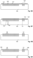
- Figures 10A-10L illustrate exemplary stages of a process of manufacturing a semiconductor device 100 in accordance with the disclosure.
- a dielectric inorganic substrate wafer 1050 is provided.
- the dielectric inorganic substrate wafer 1050 may, e.g., have a thickness of 300 to 1100 ⁇ m, in particular 400 to 700 ⁇ m.
- the dielectric inorganic substrate wafer 1050 may, e.g., be a glass wafer or a semiconductor wafer.
- Figures 1000A-L illustrate only a portion of the dielectric inorganic substrate wafer 1050 which comprises, e.g., one semiconductor chip 110, see Figure 10L .
- Figure 10B illustrates the formation of recesses 1020 in a top surface 1050A of the dielectric inorganic substrate wafer 1050.
- the recesses 1020 may be formed by etching.
- the dimensions (lateral dimensions, depths) of the recesses 1020 may correspond to the dimensions described above for the first metal structures 160.
- the dielectric inorganic substrate wafer 1050 may include (per chip) a first pattern PAT1 of recesses 1020 and a second pattern PAT2 of the recesses 1020.
- the area of PAT1 may, e.g., be substantially greater than the area of PAT2.
- the parameters (pitch, distance, shape, ...) of the recesses 1020 in PAT1 and in PAT2 may be different from each other or may be the same.
- only the first pattern PAT1 is formed as a pattern of recesses, while the second pattern PAT2 is replaced by another type of through connection such as, e.g., a single hole serving as a through connection for, e.g., the control electrode 130 of the semiconductor transistor chip 110.
- Some of the recesses 1020 formed in the dielectric inorganic substrate wafer 1050 may have a depth which is smaller than the target thickness of the dielectric inorganic substrate wafer 1050 (i.e. TS of Figure 1 ), while other recesses 1020 have a depth greater than the target thickness of the dielectric inorganic substrate wafer 1050.
- a liner 1012 may optionally be deposited over the top surface 1050A of the dielectric inorganic substrate wafer 1050.
- the liner 1012 may, e.g., be an electrically conductive seed layer.
- a protective layer 1014 may be applied over the top surface of the dielectric inorganic substrate wafer 1050 and, e.g., over the liner 1012.
- the protective layer 1014 may be applied using a self-aligned process. That is, the protective layer 1014 may only be applied over parts of the top surface 1050A of the dielectric inorganic substrate wafer 1050 which are not recessed.
- the protective layer 1014 may, e.g., be applied by a rolling and/or printing process and may, e.g., completely cover the liner 1012 at non-recessed parts of the top surface 1050A of the dielectric inorganic substrate wafer 1050.
- liner 1012 deposition and/or protective layer 1014 deposition as shown in Figures 10C and 10D are optional processes, since metal plating, as described in the following, can also be carried out without liner 1012 and/or protective layer 1014 deposition.
- metal is plated to fill the recesses 1020.
- the first metal structures 160 are formed.
- the first metal structures 160 may completely fill the recesses 1020.
- the second metal structures 170 may be formed.
- the first metal structures 160 may protrude a small distance over the top surface 1050A of the dielectric inorganic substrate wafer 1050.
- Metal plating can be carried out by electro-chemical deposition (ECD).
- ECD electro-chemical deposition
- copper or a copper alloy may be used as a plating metal, but other metals known in the art to be suitable for package interconnects can also be used.
- the same may hold true for the second metal structure(s) 170.
- the protective layer 1014 (if present) and the liner 1012 (if present) are removed by, e.g., etching.
- a bonding material 1080 may be applied on the dielectric inorganic substrate wafer 1050.
- the bonding material 1080 may be applied on areas of the dielectric inorganic substrate wafer 1050 which correspond to inactive areas of a semiconductor wafer 1010 (see Figure 10I ).
- the bonding material 1080 may e.g. comprise or be glass glue (e.g. glass frit) or a resin or any other material suitable to permanently bond the dielectric inorganic substrate wafer 1050 to the semiconductor wafer 1010 (see Figure 10I ).
- the front side of a semiconductor wafer 1010 is combined with the dielectric inorganic substrate wafer 1050 to form a composite wafer 1000.
- the plurality of patterns of first metal structures 160 is placed opposite the plurality of low voltage load electrodes 120 on the semiconductor wafer 1010.
- Figure 10I only shows a partial view of the dielectric inorganic substrate wafer 1050 and the semiconductor wafer 1010 which substantially corresponds to one semiconductor transistor chip 110 in the semiconductor wafer 1010.
- the first pattern PAT1 of first metal structures 160 and the second pattern PAT2 of second metal structures 170 may form sub-patterns corresponding to two electrodes 120, 130 of a single semiconductor transistor chip 110 of the semiconductor wafer 1010.
- the process of combining the semiconductor wafer 1010 and the dielectric inorganic substrate wafer 1050 as shown in Figure 10I may be carried out by using optical alignment through the dielectric inorganic substrate wafer 1050 (e.g. so-called through-glass alignment or through-semiconductor alignment). That is, an optical alignment processes may be carried out by viewing through the dielectric inorganic substrate wafer 1050 to recognize the position of the semiconductor wafer 1010 relative to the position of the dielectric inorganic substrate wafer 1050 so as to combine the semiconductor wafer 1010 and the dielectric inorganic substrate wafer 1050 in proper alignment.
- optical alignment processes may be carried out by viewing through the dielectric inorganic substrate wafer 1050 to recognize the position of the semiconductor wafer 1010 relative to the position of the dielectric inorganic substrate wafer 1050 so as to combine the semiconductor wafer 1010 and the dielectric inorganic substrate wafer 1050 in proper alignment.
- the bonding material 1080 may have also been applied to the semiconductor wafer 1010 rather than to the dielectric inorganic substrate wafer 1050.
- Figure 10J illustrates the process of bonding the semiconductor wafer 1010 to the dielectric inorganic substrate wafer 1050 with the front side 1010A of the semiconductor wafer 1010 facing the dielectric inorganic substrate wafer 1050.
- This process may concurrently connect the plurality of patterns of first metal structures 160 on the dielectric inorganic substrate wafer 1050 to the plurality of low voltage load electrodes 120 on the semiconductor wafer 1010.
- the process may be carried out by applying heat and pressure to the composite wafer 1000.
- the bonding 1080 material fixedly secures the semiconductor wafer 1010 to the dielectric inorganic substrate wafer 1050.
- the first metal structures 160 may be electrically and mechanically fixedly connected to the low voltage load electrodes 120.
- the connections may be solder-free, i.e. no solder material may be used for establishing the electrical, mechanical and thermal connection between the low voltage load electrodes 120 and the first metal structures 160.
- the connection may be created by the formation of an eutectic phase between the metal of the low voltage load electrodes 120 and the metal of the first metal structures 160. The same may hold true for the connection of the second metal structures 170 to the control electrodes 130.
- the dielectric inorganic substrate wafer 1050 may be thinned from a bottom surface 1050B (see Figure 10J ) opposite the top surface 1050A to expose the metal of at least a part or of all of the metal structures 160 in the recesses 1020.
- thinning may, e.g., be carried out in a multi-stage process.
- thinning may comprise grinding the dielectric inorganic substrate wafer 1050 down to a thickness which is only slightly larger than the depth of the recesses 1020.
- grinding may stop at a distance of equal to or less than 20 ⁇ m or 15 ⁇ m or 10 ⁇ m over the bottom of the recesses 1020.
- the first metal structures 160 or at least a part of them may then be exposed by etching the dielectric inorganic substrate wafer 1050 down to the thickness TS (see Figure 1 ). Etching may be carried out by wet or dry chemical etching. Etching may be continued until the first metal structures 160 (or at least some of them) and e.g. also the second metal structures 170 protrude a small distance such as, e.g., a few ⁇ m over the bottom surface of the thinned dielectric inorganic substrate wafer 1050.
- the bottom surface of the thinned dielectric inorganic substrate wafer 1050 may correspond to the bottom surface 150B of the dielectric inorganic substrate 150 as shown in Figure 1 .
- the back-end-of-line (BEOL) processes of chip packaging may be carried out on the composite wafer 1000 shown in Figure 10L .
- the composite wafer 1000 is separated along dicing lines L into composite chips corresponding to semiconductor devices 100. Separating the composite wafer 1000 into composite chips may be carried out by any suitable dicing methods, e.g. mechanical sawing, laser dicing and/or etching.
- the high voltage semiconductor transistor chip 110 and the dielectric inorganic substrate 150 may have aligned cutting edges.
Landscapes
- Engineering & Computer Science (AREA)
- Microelectronics & Electronic Packaging (AREA)
- Physics & Mathematics (AREA)
- Geometry (AREA)
- Semiconductor Integrated Circuits (AREA)
- Chemical & Material Sciences (AREA)
- Ceramic Engineering (AREA)
Abstract
Description
- This disclosure relates generally to the field of semiconductor devices, and in particular to the field of packaging semiconductor chips.
- Semiconductor device manufacturers are constantly striving to increase the performance of their products, while decreasing their cost of manufacture. A cost and device performance sensitive area in the manufacture of a semiconductor device is packaging the semiconductor chip. Packaging involves, inter alia, forming an electrical interconnect from chip electrodes (die pads) to package terminals. The interconnect technology should provide for high electrical and thermal performance and reliability of the semiconductor device.
- Packaging of high voltage (HV) semiconductor chips involves a number of specific problems. For example, the high-voltage edge of the chip is very sensitive, and any change in the vicinity of the high-voltage edge may adversely affect the edge termination of the chip. For example, there must be a relatively large distance between the semiconductor chip edge and a low-voltage terminal element (e.g., source terminal element or gate terminal element) that crosses the chip edge to allow lateral exit of field lines between the chip edge and the low-voltage terminal element.
- Further aspects aim at cost efficient manufacturing processes and customer benefits in view of product versatileness and package mountability.
- According to an aspect of the disclosure a high voltage semiconductor package comprises a semiconductor device. The semiconductor device comprises a high voltage semiconductor transistor chip comprising a front side and a backside. A low voltage load electrode and a control electrode are disposed on the front side of the semiconductor transistor chip. A high voltage load electrode is disposed on the backside of the semiconductor transistor chip. The semiconductor package further comprises a dielectric inorganic substrate. The dielectric inorganic substrate comprises a pattern of first metal structures running through the dielectric inorganic substrate, wherein the pattern of first metal structures is connected to the low voltage load electrode, and at least one second metal structure running through the dielectric inorganic substrate, wherein the second metal structure is connected to the control electrode. The front side of the semiconductor transistor chip is attached to the dielectric inorganic substrate by a wafer bond connection, and the dielectric inorganic substrate has a thickness of at least 50 µm.
- The elements of the drawings are not necessarily to scale relative to each other. Like reference numerals designate corresponding similar parts. The features of the various illustrated embodiments can be combined unless they exclude each other and/or can be selectively omitted if not described to be necessarily required. Embodiments are depicted in the drawings and are exemplarily detailed in the description which follows.
-
Figure 1 is a schematic cross-sectional view of an exemplary semiconductor device comprising a semiconductor chip and a dielectric inorganic substrate in accordance with the disclosure. -
Figure 2A is a cross-sectional view of the dielectric inorganic substrate along line X-X ofFigure 1 . -
Figure 2B is a partial view of a detail D ofFigure 1 and 2A . -
Figure 3 is a schematic cross-sectional view of an exemplary leadframe package including a semiconductor chip and a dielectric inorganic substrate in accordance with the disclosure. -
Figure 4 is a top view of an exemplary leadframe ofFigure 3 . -
Figure 5 is a top view illustrating the cross-sectional view of the dielectric inorganic substrate ofFigure 2A when positioned over the leadframe. -
Figure 6 is a schematic cross-sectional view of an exemplary on-board assembly of a semiconductor chip and a dielectric inorganic substrate in accordance with the disclosure. -
Figure 7 is a schematic cross-sectional view of an example of a laminate embedded chip package including a semiconductor chip and a dielectric inorganic substrate in accordance with the disclosure. -
Figure 8 is a schematic cross-sectional view of an example of a laminate embedded chip package including a semiconductor chip and a dielectric inorganic substrate in accordance with the disclosure. -
Figure 9 is a schematic cross-sectional view of a dielectricinorganic substrate 150 including a plurality of stacked dielectric inorganic substrate layers. -
Figures 10A-10L are schematic cross-sectional views illustrating exemplary stages of manufacturing an exemplary semiconductor device in accordance with the disclosure. - As used in this specification, the terms "electrically connected" or "connected" or similar terms are not meant to mean that the elements are directly contacted together; intervening elements may be provided between the "electrically connected" or "connected" elements, respectively. However, in accordance with the disclosure, the above-mentioned and similar terms may, optionally, also have the specific meaning that the elements are directly contacted together, i.e. that no intervening elements are provided between the "electrically connected" or "connected" elements, respectively.
- Further, the words "over" or "beneath" with regard to a part, element or material layer formed or located "over" or "beneath" a surface may be used herein to mean that the part, element or material layer be located (e.g. placed, formed, arranged, deposited, etc.) "directly on" or "directly under", e.g. in direct contact with, the implied surface. The word "over" or "beneath" used with regard to a part, element or material layer formed or located "over" or "beneath" a surface may, however, either be used herein to mean that the part, element or material layer be located (e.g. placed, formed, arranged, deposited, etc.) "indirectly on" or "indirectly under" the implied surface, with one or more additional parts, elements or layers being arranged between the implied surface and the part, element or material layer.
-
Figure 1 illustrates a schematic cross-sectional view of anexemplary semiconductor device 100. Thesemiconductor device 100 includes asemiconductor transistor chip 110. Thesemiconductor transistor chip 110 is a high voltage semiconductor transistor chip that operates at a supply voltage (e.g. drain voltage) equal to or higher than, e.g., 100 V, 200 V, 300 V, 400 V, 500 V, 600 V, 700 V, 800 V, 900 V, or 1000 V. In particular, thesemiconductor transistor chip 110 may operate at a supply voltage in a range between 300 V and 800 V. - The
semiconductor transistor chip 110 may be a vertical transistor device. Thesemiconductor transistor chip 110 has afront side 110A and abackside 110B. A lowvoltage load electrode 120 and acontrol electrode 130 are disposed on thefront side 110A of thesemiconductor transistor chip 110, and a highvoltage load electrode 140 is disposed on thebackside 110B of thesemiconductor transistor chip 110. - The
semiconductor transistor chip 110 may, e.g., be made of any semiconductor material, e.g. Si, SiC, SiGe, GaAs, GaN, AlGaN, InGaAs, InAlAs, etc. In particular, high voltage Si orSiC transistor chips 110 are considered herein. - A dielectric
inorganic substrate 150 is attached to thefront side 110A of thesemiconductor transistor chip 110. More specifically, thefront side 110A of thesemiconductor transistor chip 110 is attached to atop surface 150A of the dielectricinorganic substrate 150 by awafer bond connection 180. Thefront side 110A of thesemiconductor transistor chip 110 may be completely covered by the dielectricinorganic substrate 150. In particular, the dielectricinorganic substrate 150 may be a glass substrate and thewafer bond connection 180 may, e.g., be a glass frit connection. - The dielectric
inorganic substrate 150 comprises a pattern offirst metal structures 160. Thefirst metal structures 160 may be accommodated in recesses of the dielectricinorganic substrate 150. Thefirst metal structures 160 run through the dielectricinorganic substrate 150, wherein the pattern offirst metal structures 160 is connected to the lowvoltage load electrode 120. - The dielectric
inorganic substrate 150 further comprises at least onesecond metal structure 170 running through the dielectricinorganic substrate 150. Thesecond metal structure 170 is connected to thecontrol electrode 130. - The first and
second metal structures inorganic substrate 150 and the first andsecond metal structures inorganic substrate 150 by metal plating. - The dielectric
inorganic substrate 150 may be a glass substrate or a semiconductor substrate. If themetal structures 160 are required to be electrically insulated from each other, glass or an intrinsic semiconductor substrate material or a semiconductor substrate having recesses with insulated side walls could be used. Recesses with insulated side walls may, e.g., be formed by applying an insulating layer (e.g. a silicon oxide layer or a silicon nitride layer) to the side walls of the recesses in which the first andsecond metal structures - The
semiconductor device 100 may be referred to as a composite chip or substrate-semiconductor hetero-structure. Such composite chip may be diced out of a composite wafer which may comprise a semiconductor wafer and a dielectric inorganic substrate wafer bonded together by a wafer bond connection. - Such composite chips offer a number of advantages, especially for the packaging of high voltage transistor chips.
- First, by integrating the permanent dielectric
inorganic substrate 150 together with thesemiconductor transistor chip 110 in a package, the dielectricinorganic substrate 150 may be used as an "adapter" that can be appropriately structured and metallized to make the composite chip directly solderable to a leadframe or application board or another terminal structure of a given geometry. For example, thefirst metal structures 160 may end in asubstrate metallization 120M representing the lowvoltage load electrode 120 of the semiconductor device (composite chip) 100 and extending on abottom surface 150B of the dielectricinorganic substrate 150. Accordingly, the one or moresecond metal structures 170 may end in asubstrate metallization 130M which represents thecontrol electrode 130 of the semiconductor device (composite chip) 100. As thesubstrate metallizations semiconductor transistor chip 110, constrains in terms of their geometries are substantially relaxed. For this and for other reasons, the geometries of the (low voltage)substrate metallizations voltage load electrode 120 and thecontrol electrode 130, respectively. - In other words, the dielectric
inorganic substrate 150 may be useful as a "chip electrode layout adaptor" between thesemiconductor transistor chip 110 and a terminal geometry provided internal (e.g. by a leadframe) or external (e.g. by an application board) of a high voltage semiconductor package which includes thesemiconductor device 100. This allows direct bonding of the "adapted" chip front side electrodes (namely thesubstrate metallizations - As a second aspect, the implementation of the dielectric
inorganic substrate 150 allows to process very thin semiconductor wafers when being supported by the dielectric inorganic substrate wafer. Therefore, high voltagesemiconductor transistor chips 110 with advanced electrical and thermal properties may be used. - Third, it is to be noted that in the case of high voltage
semiconductor transistor chips 110, there needs to be a relatively large spacing between thefront side 110A of thesemiconductor transistor chip 110 and a low voltage connection element (e.g. low voltage load electrode connection element or control electrode connection element) that extends laterally across the edge of thesemiconductor transistor chip 110. This spacing is required because the chip edge together with thebackside 110B of thesemiconductor transistor chip 110 is at a rapidly changing high voltage potential. For example, while the voltage fluctuations at thefront side 110A of thesemiconductor transistor chip 110 are, e.g., between 0.1 - 3 V at the low voltage load electrode and, e.g., between 0 - 20 V at the control electrode, the voltage fluctuations at the backside 100B and the edge of thesemiconductor transistor chip 110 are between 0 V and e.g. 300 to 800 V or even 1000 V with a frequency of several 100 kHz. The relatively large spacing between thefront side 110A of thesemiconductor transistor chip 110 and low voltage connecting elements or terminals (e.g. leadframe or application board or conductor traces of a laminate) extending across the edge of thesemiconductor transistor chip 110 allow the field lines to escape laterally between the low voltage connecting elements and the chip edge. - This distance is created by providing the dielectric
inorganic substrate 150 with a sufficient thickness TS. Thus, the dielectricinorganic substrate 150 acts as an "extension" to allow field lines to exit laterally between low voltage terminal elements and the chip edge. For example, the dielectricinorganic substrate 150 may have a thickness TS which may be equal to or greater than or less than 50 µm or 100 µm or 200 µm or 300 µm or 400 µm. While for SiC or other high bandgap semiconductor materials, a thickness TS of 50 µm may, e.g., be sufficient, Sisemiconductor transistor chips 110 advantageously may use a dielectricinorganic substrate 150 of a thickness TS of equal to or greater than 100 µm. - The
bottom surface 150B of the dielectricinorganic substrate 150 may be (highly) planar. Thebottom surface 150B of the dielectricinorganic substrate 150 may be parallel with thebackside 110B of thesemiconductor transistor chip 110. - As apparent from
Figures 2A and 2B , thefirst metal structures 160 may be arranged in a densely packed array in the dielectricinorganic substrate 150. Differently put, the dielectricinorganic substrate 150 may form a matrix for the pattern or array offirst metal structures 160. The percentage in volume of metal within the pattern or array of thefirst metal structures 160 in the dielectricinorganic substrate 150 may be high, e.g. equal to or greater than, e.g., 40% or 50% or 60% or 70% or 80%. - The pattern of
first metal structures 160 may, e.g., be a regular array. A pitch of the pattern offirst metal structures 160 may, e.g., be equal to or greater than or less than 15 µm or 17.5 µm or 20 µm or 22.5 µm or 25 µm or 27.5 µm or 30 µm. A distance between adjacentfirst metal structures 160 may, e.g., be equal to or greater than or less than 50 µm or 30 µm or 10 µm or 5 µm or 4 µm or 3 µm or 2 µm. The lateral dimension(s) of eachfirst metal structure 160 may, e.g., be equal to or greater than or less than 12.5 µm or 15 µm or 17.5 µm or 20 µm or 22.5 µm or 25 µm or 27.5 µm. A a ratio of a distance between adjacentfirst metal structures 160 and a lateral dimension (e.g. diameter) of afirst metal structure 160 may be equal to or less than 5 or 3 or 2 or 1. - Referring to
Figure 2A , the dielectricinorganic substrate 150 may, e.g., have a polygonal, in particular rectangular shape. - By virtue of the dielectric
inorganic substrate 150, thesemiconductor device 110 may have advanced heat dissipation properties. Heat dissipation insemiconductor devices 100 relies, inter alia, on the electrical interconnect between thesemiconductor transistor chip 110 and a terminal structure (e.g. leadframe or application board or conductor traces of a laminate, etc.) on which thesemiconductor chip 110 is mounted. Here, this electrical interconnect includes or is composed of the pattern offirst metal structures 160 in the dielectricinorganic substrate 150. The pattern offirst metal structures 160 can be optimized in terms of thermal conductivity and/or heat capacity. The more densely thefirst metal structures 160 are packed in the dielectricinorganic substrate 150, the better the heat conductivity and the thermal capacity of the dielectricinorganic substrate 150. Further, enhancing the thickness TS of the dielectricinorganic structure 150 increases the thermal capacity thereof, because more metal is held available in the dielectricinorganic structure 150 for transient heat absorption. - The
second metal structures 170 may be implemented the same way as described above for thefirst metal structures 160, and reiteration is avoided for the sake of brevity. However, as the second metal structure(s) 170 connect(s) to a low current control electrode, it is also possible that only a single second metal structure (i.e. a single metal pillar connecting between thecontrol electrode 130 and thesubstrate metallization 130M of the control electrode) is sufficient. - Returning to
Figure 2B , thefirst metal structures 160 may, e.g., have a polygonal (square, hexagonal, etc.) or rounded cross-section. A square cross-sectional shape is exemplarily shown inFigure 2B , whileFigure 2A illustrates for example a rounded cross-sectional shape. A hexagonal cross-sectional shape may be beneficial as it provides for a particular high area packing density of metal in the dielectricinorganic structure 150. - Each
first metal structure 160 may be linear and/or have an axially symmetric cross-sectional shape. Furthermore, eachfirst metal structure 160 may, e.g., have a substantially constant cross-sectional shape along its extension through the dielectricinorganic substrate 150. Variable-cross sectional shapes along the longitudinal extension such as, e.g., tapering shapes or bulges or thickenings are also possible. - Moreover, the pattern does not need to be designed as a regular array. Rather, the pattern may be composed of a plurality of different patterns or (e.g. regular) arrays. Such different patterns (e.g. sub-patterns) or arrays (e.g. sub-arrays) may distinguish from each other e.g. in terms of pitch and/or cross-sectional shape of the
first metal structures 160. -
Figure 3 illustrates an example of aleadframe package 300. Theleadframe package 300 includes aleadframe 310 having a first leadframe pad 310_1 and a second leadframe pad 310_2. Asemiconductor device 100, as described above, is bonded to theleadframe 310. More specifically, the pattern offirst metal structures 160 is bonded to the first leadframe pad 310_1 and the at least onesecond metal structure 170 is bonded to thesecond leadframe pad 310 2. - As shown in
Figure 3 , theleadframe package 300 relies on a low voltage electrode-down approach. In the following, without loss of generality, the lowvoltage load electrode 120 is exemplified by the source electrode of thesemiconductor transistor chip 110 and thecontrol electrode 130 is exemplified by the gate electrode of thesemiconductor transistor chip 110. Hence, the low voltage electrode-down approach is referred to as a source-down approach in the following. - The source-down approach of the
leadframe package 300 solves another problem of high voltage applications. Conventionally the heat sink is always coupled to the drain (here the backside high voltage load electrode 140). In this case, the heat sink must be constantly charged or discharged or, if the heat sink is capacitively coupled to thedrain 140, losses occur due to the capacitive coupling. Both these types of losses (charge/discharge losses or capacitive losses) with regard to the heat sink and further high frequency electro magnetic interference (EMI) behavior, which inevitably occurs due the large area of thedrain 140 electrode, are major disadvantages for high voltage leadframe packages. - With the source-down approach of
Figure 3 , these problems are solved. This is because thesemiconductor transistor chip 110 has its source connected to thelead frame 310 via the dielectricinorganic substrate extension 150, and thus also to the heat sink. As mentioned before, the source is always at a low potential, i.e. does not constantly fluctuate between zero and high voltage. - The
leadframe package 300 may include a package body formed of a molded encapsulation material (not shown). Further, theleadframe package 300 may include an electricallyconductive element 340 bonded to the high voltage load electrode (e.g. drain electrode) 140. The electricallyconductive element 340 may, e.g., be a clip or a ribbon or a plurality of bond wires which connect to a high voltage terminal (not shown) of the highvoltage leadframe package 300. - As noted above, the
leadframe 310 can have a variety of different geometries (e.g., seeFigure 4 for a specific example) that can be easily modified due to the geometric adaptability provided by the dielectricinorganic substrate 150. -
Figure 5 illustrates an exemplary position of the dielectricinorganic substrate 150 over theleadframe 310 in a top view representation. The outline of the low voltage load electrode 120 (e.g. source electrode) is indicated by dashedline 520 and the outline of thecontrol electrode 130 is indicated by dashedline 530. It is apparent that the dielectricinorganic substrate 150 allows to use a leadframe geometry which could not be used if theleadframe 310 would be directly soldered to thesemiconductor transistor chip 110. Further, as the first leadframe pad 310_1 represents the thermal pad of theleadframe 310, the source-down approach ofFigures 3 to 5 allows to contact the lowvoltage load electrode 120 via thefirst metal structures 160 with high thermal conductivity to a heat sink (namely the first leadframe pad 310_1) without charging/discharging or capacitive losses and improved EMI behavior. - Referring to
Figure 6 , thesemiconductor device 100 may be directly mounted (e.g. soldered) to anapplication board 610. More specifically, the low voltage loadelectrode substrate metallization 120M and the controlelectrode substrate metallization 130M may be electrically and mechanically fixed by a bond material 620 (e.g. solder, conductive adhesive, sinter material, ...) to conductor traces (not shown) provided on theapplication board 610. - Analogously as described above, the
semiconductor device 100 may be packaged by using e.g. an electrically conductive element 340 (not shown inFigure 6 ) and/or a molded encapsulant. Reference is made to the above description to avoid reiteration. -
Figure 7 illustrates an example of a laminate embeddedchip package 700. The laminate embeddedchip package 700 includes alaminate structure 710 for semiconductor device embedding. Thesemiconductor device 100 is embedded in thelaminate structure 710. - The
laminate structure 710 may, e.g., be a printed circuit board (PCB). A PCB may includeconductive layers laminate layer 750. Thelaminate layer 750 provides for electrical insulation and mechanical support of theconductive layers conductive layers laminate structure 710. Thelaminate structure 710 may, e.g., be a FR-4 PCB. - The laminate embedded
chip package 700 may be formed by a variety of laminate and chip embedding processes. For example, thelaminate structure 710 may be formed by a PCB, which is recessed, and thesemiconductor device 100 is then placed into the recess. - Another possibility is to first place the semiconductor device 100 (composite chip) on a base carrier represented in
Figure 7 by theconductive layer 720. This base carrier may be a metal plate or a leadframe. Thesemiconductor device 100 may be bonded to this base carrier by known techniques such as using printable conductive pastes or soldering. Following the process of bonding thesemiconductor device 100 to the base carrier (e.g. conductive layer 720), thelaminate layer 750 may be vacuum laminated on the base carrier. In other words, thesemiconductor device 100 bonded to a leadframe (e.g. a structured or unstructured metal plate of a thickness of, e.g., equal to or greater than 150 µm) is subjected to a lamination process for packaging. Subsequently to the lamination, via contacts (not shown) to thebase carrier 720 and to thesubstrate metallizations semiconductor device 100 to external terminals. -
Figure 8 illustrates an example of a further laminate embeddedchip package 800. In this example, thelaminate structure 710 is a core laminate structure of the embeddedchip package 800. The laminate embeddedchip package 800 further comprises a bottom laminate structure 810_1 extending below thecore laminate structure 710 and thesemiconductor device 100. Alternatively or in addition, the laminate embeddedchip package 800 may be provided with a top laminate structure 810_2 extending above thecore laminate structure 710 and thesemiconductor device 100. Further,conductive layers 820 and/or 830 may be provided on the bottom laminate structure 810_1 and/or the top laminate structure 810_2. Theseconductive layers conductive layers semiconductor device 100 to external circuitry. Here, e.g. the structuredconductive layer 730 forms electrical contacts to thesemiconductor device 100 which are disconnected from each other and embedded in dielectric material (laminate layer 750 and top laminate structure 810_2). Further, as described above for laminate embeddedchip package 700, also in laminate embeddedchip package 800 thesemiconductor device 100 can be pre-bonded to a (structured or unstructured) leadframe (instead of conductive layer 720) and then accommodated in the laminate embeddedchip package 800 by combinedsemiconductor device 100 and leadframe lamination. The (structured or unstructured) leadframe or theconductive layer 720 and/or theconductive layer 730 may have a thickness of, e.g., equal to or greater than 150 µm. - Laminate embedded
chip packages inorganic substrate 150. The dielectricinorganic substrate 150 guarantees for a sufficient spacing between the chip edge and theconductive layer 730 extending across the chip edge. Without the dielectricinorganic substrate 150 this spacing would need to be provided by other means, e.g. by a relatively thick laminate spacing layer applied instead of the dielectricinorganic substrate 150. However, such thick laminate spacing layers cause difficulties in the embedding process. It is much more convenient in view of process and device reliability to use thesemiconductor transistor chip 110 with the pre-mounted dielectric inorganic substrate spacer as an object to be laminated. Hence, the "composite chip" approach applied to chip embedding in laminate chip packages makes the manufacturing process of such HV packages much easier and more reliable. - Referring to
Figure 9 , the dielectricinorganic substrate 150 may comprise or be composed of a plurality of stacked dielectric inorganic substrate layers 150_1, 150_2, 150_3. Each dielectric inorganic substrate layer 150_1, 150_2, 150_3 may be constructed the same way as described for the dielectricinorganic substrate 150. Implementing the dielectricinorganic substrate 150 by a multi-layer structure, as shown inFigure 9 , may facilitate the process of manufacturing thick dielectricinorganic substrates 150, since recess formation and metal plating can be carried out more conveniently with thinner structures, namely the layers 150_1, 150_2 and 150_3. For instance, if a thickness TS of 300 µm is desired, each of these processes need only to be carried out on a dielectric inorganic substrate layer 150_1, 150_2, 150_3 of a thickness of, e.g.,50 µm or 100 µm. - The dielectric inorganic substrate layers 150_1, 150_2, 150_3 including the first and
second metal structures inorganic substrate 150. As noted before, layer bonding may be done on wafer-level e.g. by using a glass frit connection between adjacent dielectric inorganic substrate layers 150_1, 150_2 and 150_3. - Further, this technique of stacking a plurality of dielectric inorganic substrate layers 150_1, 150_2, 150_3 allows to form
third metal structures 960 which do not extend through the dielectricinorganic substrate 150 but end in the dielectricinorganic substrate 150 at a dielectric inorganic substrate layer 150_1, 150_2 adjacent to the dielectric inorganic substrate layer 150_2, 150_3 which is provided with thethird metal structure 960. Suchthird metal structures 960 can be used as field plates (e.g. source field plates) which allow to appropriately effect the electrical field above thesemiconductor transistor chip 110. Due to the layer-by-layer arrangement of the dielectricinorganic substrate 150, no blind holes need to be fabricated to realize suchthird metal structures 960 terminating in the dielectricinorganic substrate 150. -
Figures 10A-10L illustrate exemplary stages of a process of manufacturing asemiconductor device 100 in accordance with the disclosure. - Referring to
Figure 10A , a dielectricinorganic substrate wafer 1050 is provided. The dielectricinorganic substrate wafer 1050 may, e.g., have a thickness of 300 to 1100 µm, in particular 400 to 700 µm. The dielectricinorganic substrate wafer 1050 may, e.g., be a glass wafer or a semiconductor wafer. Figures 1000A-L illustrate only a portion of the dielectricinorganic substrate wafer 1050 which comprises, e.g., onesemiconductor chip 110, seeFigure 10L . -
Figure 10B illustrates the formation ofrecesses 1020 in atop surface 1050A of the dielectricinorganic substrate wafer 1050. Therecesses 1020 may be formed by etching. The dimensions (lateral dimensions, depths) of therecesses 1020 may correspond to the dimensions described above for thefirst metal structures 160. - According to
Figure 10B , the dielectricinorganic substrate wafer 1050 may include (per chip) a first pattern PAT1 ofrecesses 1020 and a second pattern PAT2 of therecesses 1020. As shown on the right hand side ofFigure 10B which illustrates a top view on a chip portion of the dielectricinorganic substrate wafer 1050, the area of PAT1 may, e.g., be substantially greater than the area of PAT2. Further, as mentioned before, the parameters (pitch, distance, shape, ...) of therecesses 1020 in PAT1 and in PAT2 may be different from each other or may be the same. - In one embodiment, only the first pattern PAT1 is formed as a pattern of recesses, while the second pattern PAT2 is replaced by another type of through connection such as, e.g., a single hole serving as a through connection for, e.g., the
control electrode 130 of thesemiconductor transistor chip 110. - Some of the
recesses 1020 formed in the dielectricinorganic substrate wafer 1050 may have a depth which is smaller than the target thickness of the dielectric inorganic substrate wafer 1050 (i.e. TS ofFigure 1 ), whileother recesses 1020 have a depth greater than the target thickness of the dielectricinorganic substrate wafer 1050. - Referring to
Figure 10C , aliner 1012 may optionally be deposited over thetop surface 1050A of the dielectricinorganic substrate wafer 1050. Theliner 1012 may, e.g., be an electrically conductive seed layer. - Referring to
Figure 10D , aprotective layer 1014 may be applied over the top surface of the dielectricinorganic substrate wafer 1050 and, e.g., over theliner 1012. Theprotective layer 1014 may be applied using a self-aligned process. That is, theprotective layer 1014 may only be applied over parts of thetop surface 1050A of the dielectricinorganic substrate wafer 1050 which are not recessed. Theprotective layer 1014 may, e.g., be applied by a rolling and/or printing process and may, e.g., completely cover theliner 1012 at non-recessed parts of thetop surface 1050A of the dielectricinorganic substrate wafer 1050. - It is to be noted that the processes of
liner 1012 deposition and/orprotective layer 1014 deposition as shown inFigures 10C and 10D are optional processes, since metal plating, as described in the following, can also be carried out withoutliner 1012 and/orprotective layer 1014 deposition. - Referring to
Figure 10F , metal is plated to fill therecesses 1020. As a result, thefirst metal structures 160 are formed. Thefirst metal structures 160 may completely fill therecesses 1020. Further, thesecond metal structures 170 may be formed. - The
first metal structures 160 may protrude a small distance over thetop surface 1050A of the dielectricinorganic substrate wafer 1050. Metal plating can be carried out by electro-chemical deposition (ECD). For instance, copper or a copper alloy may be used as a plating metal, but other metals known in the art to be suitable for package interconnects can also be used. The same may hold true for the second metal structure(s) 170. - Referring to
Figure 10G , the protective layer 1014 (if present) and the liner 1012 (if present) are removed by, e.g., etching. - Referring to
Figure 10H , abonding material 1080 may be applied on the dielectricinorganic substrate wafer 1050. Thebonding material 1080 may be applied on areas of the dielectricinorganic substrate wafer 1050 which correspond to inactive areas of a semiconductor wafer 1010 (seeFigure 10I ). - The
bonding material 1080 may e.g. comprise or be glass glue (e.g. glass frit) or a resin or any other material suitable to permanently bond the dielectricinorganic substrate wafer 1050 to the semiconductor wafer 1010 (seeFigure 10I ). - Referring to
Figure 10I , the front side of asemiconductor wafer 1010 is combined with the dielectricinorganic substrate wafer 1050 to form acomposite wafer 1000. During this process the plurality of patterns offirst metal structures 160 is placed opposite the plurality of lowvoltage load electrodes 120 on thesemiconductor wafer 1010. Again, it is to be noted thatFigure 10I only shows a partial view of the dielectricinorganic substrate wafer 1050 and thesemiconductor wafer 1010 which substantially corresponds to onesemiconductor transistor chip 110 in thesemiconductor wafer 1010. Hence, the first pattern PAT1 offirst metal structures 160 and the second pattern PAT2 ofsecond metal structures 170 may form sub-patterns corresponding to twoelectrodes semiconductor transistor chip 110 of thesemiconductor wafer 1010. - The process of combining the
semiconductor wafer 1010 and the dielectricinorganic substrate wafer 1050 as shown inFigure 10I may be carried out by using optical alignment through the dielectric inorganic substrate wafer 1050 (e.g. so-called through-glass alignment or through-semiconductor alignment). That is, an optical alignment processes may be carried out by viewing through the dielectricinorganic substrate wafer 1050 to recognize the position of thesemiconductor wafer 1010 relative to the position of the dielectricinorganic substrate wafer 1050 so as to combine thesemiconductor wafer 1010 and the dielectricinorganic substrate wafer 1050 in proper alignment. - The
bonding material 1080 may have also been applied to thesemiconductor wafer 1010 rather than to the dielectricinorganic substrate wafer 1050. -
Figure 10J illustrates the process of bonding thesemiconductor wafer 1010 to the dielectricinorganic substrate wafer 1050 with thefront side 1010A of thesemiconductor wafer 1010 facing the dielectricinorganic substrate wafer 1050. This process may concurrently connect the plurality of patterns offirst metal structures 160 on the dielectricinorganic substrate wafer 1050 to the plurality of lowvoltage load electrodes 120 on thesemiconductor wafer 1010. The process may be carried out by applying heat and pressure to thecomposite wafer 1000. - By virtue of this process the
bonding 1080 material fixedly secures thesemiconductor wafer 1010 to the dielectricinorganic substrate wafer 1050. Further, by this or another process, thefirst metal structures 160 may be electrically and mechanically fixedly connected to the lowvoltage load electrodes 120. The connections may be solder-free, i.e. no solder material may be used for establishing the electrical, mechanical and thermal connection between the lowvoltage load electrodes 120 and thefirst metal structures 160. By way of example, the connection may be created by the formation of an eutectic phase between the metal of the lowvoltage load electrodes 120 and the metal of thefirst metal structures 160. The same may hold true for the connection of thesecond metal structures 170 to thecontrol electrodes 130. - Referring to
Figures 10K and10L , the dielectricinorganic substrate wafer 1050 may be thinned from abottom surface 1050B (seeFigure 10J ) opposite thetop surface 1050A to expose the metal of at least a part or of all of themetal structures 160 in therecesses 1020. - More specifically, thinning may, e.g., be carried out in a multi-stage process. For instance, as shown in
Figure 10K , thinning may comprise grinding the dielectricinorganic substrate wafer 1050 down to a thickness which is only slightly larger than the depth of therecesses 1020. For instance, grinding may stop at a distance of equal to or less than 20 µm or 15 µm or 10 µm over the bottom of therecesses 1020. - The
first metal structures 160 or at least a part of them may then be exposed by etching the dielectricinorganic substrate wafer 1050 down to the thickness TS (seeFigure 1 ). Etching may be carried out by wet or dry chemical etching. Etching may be continued until the first metal structures 160 (or at least some of them) and e.g. also thesecond metal structures 170 protrude a small distance such as, e.g., a few µm over the bottom surface of the thinned dielectricinorganic substrate wafer 1050. The bottom surface of the thinned dielectricinorganic substrate wafer 1050 may correspond to thebottom surface 150B of the dielectricinorganic substrate 150 as shown inFigure 1 . - In the following, the back-end-of-line (BEOL) processes of chip packaging may be carried out on the
composite wafer 1000 shown inFigure 10L . In this context, thecomposite wafer 1000 is separated along dicing lines L into composite chips corresponding tosemiconductor devices 100. Separating thecomposite wafer 1000 into composite chips may be carried out by any suitable dicing methods, e.g. mechanical sawing, laser dicing and/or etching. As a result, the high voltagesemiconductor transistor chip 110 and the dielectricinorganic substrate 150 may have aligned cutting edges. - The following examples pertain to further aspects of the disclosure:
- Example 1 is a high voltage semiconductor package, comprising a semiconductor device comprising a high voltage semiconductor transistor chip comprising a front side and a backside, wherein a low voltage load electrode and a control electrode are disposed on the front side of the semiconductor transistor chip and a high voltage load electrode is disposed on the backside of the semiconductor transistor chip; a dielectric inorganic substrate comprising a pattern of first metal structures running through the dielectric inorganic substrate, wherein the pattern of first metal structures is connected to the low voltage load electrode; and at least one second metal structure running through the dielectric inorganic substrate, wherein the second metal structure is connected to the control electrode; wherein the front side of the semiconductor transistor chip is attached to the dielectric inorganic substrate by a wafer bond connection, and the dielectric inorganic substrate has a thickness of at least 50 µm.
- In Example 2, the subject matter of Example 1 can optionally include wherein a leadframe comprising a first leadframe pad and a second leadframe pad; and the semiconductor device, wherein the dielectric inorganic substrate is bonded to the leadframe, wherein the pattern of first metal structures is bonded to the first leadframe pad and the at least one second metal structure is bonded to the second leadframe pad.
- In Example 3, the subject matter of Example 2 can optionally include wherein the first leadframe pad forms a low voltage terminal, in particular source terminal, of the high voltage semiconductor package and the second leadframe pad forms a control terminal, in particular gate terminal, of the high voltage semiconductor package.
- In Example 4, the subject matter of Example 2 or 3 can optionally include an electrically conductive element bonded to the high voltage load electrode of the semiconductor transistor chip and connecting to a high voltage terminal of the high voltage semiconductor package.
- In Example 5, the subject matter of Example 1 can optionally include wherein a laminate structure for semiconductor device embedding, wherein the semiconductor device is embedded in the laminate structure.
- In Example 6, the subject matter of Example 5 can optionally include wherein the laminate structure is a printed circuit board.
- In Example 7, the subject matter of Example 5 or 6 can optionally include wherein the laminate structure is a core laminate structure, the high voltage semiconductor package further comprising a bottom laminate structure extending below the core laminate structure and the semiconductor device; and/or a top laminate structure extending above the core laminate structure and the semiconductor device.
- In Example 8, the subject matter of any of the preceding Examples can optionally include wherein the dielectric inorganic substrate is a glass substrate.
- In Example 9, the subject matter of Example 8 can optionally include wherein the wafer bond connection is a glass frit connection.
- In Example 10, the subject matter of any of the preceding Examples can optionally include wherein the first metal structures are connected to the low voltage load electrode by a metal-to-metal wafer bond connection, and/or the second metal structure is connected to the control electrode by a metal-to-metal wafer bond connection.
- In Example 11, the subject matter of any of the preceding Examples can optionally include wherein the dielectric inorganic substrate comprises a plurality of stacked dielectric inorganic substrate layers.
- In Example 12, the subject matter of any of the preceding Examples can optionally include wherein the first metal structures are plated metal pillars.
- In Example 13, the subject matter of any of the preceding Examples can optionally include wherein the pattern is a regular array.
- In Example 14, the subject matter of any of the preceding Examples can optionally include wherein a ratio of a distance between adjacent first metal structures and a lateral dimension (e.g. diameter) of a first metal structure is equal to or less than 5 or 3 or 2 or 1.
- In Example 15, the subject matter of any of the preceding Examples can optionally include wherein the front side of the semiconductor transistor chip is completely covered by the dielectric inorganic substrate.
- Although specific embodiments have been illustrated and described herein, it will be appreciated by those of ordinary skill in the art that a variety of alternate and/or equivalent implementations may be substituted for the specific embodiments shown and described without departing from the scope of the present invention. This application is intended to cover any adaptations or variations of the specific embodiments discussed herein. Therefore, it is intended that this invention be limited only by the claims and the equivalents thereof.
Claims (15)
- A high voltage semiconductor package, comprising:a semiconductor device comprisinga high voltage semiconductor transistor chip comprising a front side and a backside, wherein a low voltage load electrode and a control electrode are disposed on the front side of the semiconductor transistor chip and a high voltage load electrode is disposed on the backside of the semiconductor transistor chip;a dielectric inorganic substrate comprisinga pattern of first metal structures running through the dielectric inorganic substrate, wherein the pattern of first metal structures is connected to the low voltage load electrode; andat least one second metal structure running through the dielectric inorganic substrate, wherein the second metal structure is connected to the control electrode; whereinthe front side of the semiconductor transistor chip is attached to the dielectric inorganic substrate by a wafer bond connection, andthe dielectric inorganic substrate has a thickness of at least 50 µm.
- The high voltage semiconductor package of claim 1, further comprising:a leadframe comprising a first leadframe pad and a second leadframe pad; andthe semiconductor device, wherein the dielectric inorganic substrate is bonded to the leadframe, wherein the pattern of first metal structures is bonded to the first leadframe pad and the at least one second metal structure is bonded to the second leadframe pad.
- The high voltage semiconductor package of claim 2, wherein the first leadframe pad forms a low voltage terminal, in particular source terminal, of the high voltage semiconductor package and the second leadframe pad forms a control terminal, in particular gate terminal, of the high voltage semiconductor package.
- The high voltage semiconductor package of claim 2 or 3, further comprising:
an electrically conductive element bonded to the high voltage load electrode of the semiconductor transistor chip and connecting to a high voltage terminal of the high voltage semiconductor package. - The high voltage semiconductor package of claim 1, further comprising:
a laminate structure for semiconductor device embedding, wherein the semiconductor device is embedded in the laminate structure. - The high voltage semiconductor package of claim 5, wherein the laminate structure is a printed circuit board.
- The high voltage semiconductor package of claim 5 or 6, wherein the laminate structure is a core laminate structure, the high voltage semiconductor package further comprising:a bottom laminate structure extending below the core laminate structure and the semiconductor device; and/ora top laminate structure extending above the core laminate structure and the semiconductor device.
- The high voltage semiconductor package of any of the preceding claims, wherein the dielectric inorganic substrate is a glass substrate.
- The high voltage semiconductor package of claim 8, wherein the wafer bond connection is a glass frit connection.
- The high voltage semiconductor package of any of the preceding claims, wherein the first metal structures are connected to the low voltage load electrode by a metal-to-metal wafer bond connection, and/or the second metal structure is connected to the control electrode by a metal-to-metal wafer bond connection.
- The high voltage semiconductor package of any of the preceding claims, wherein the dielectric inorganic substrate comprises a plurality of stacked dielectric inorganic substrate layers.
- The high voltage semiconductor package of any of the preceding claims, wherein the first metal structures are plated metal pillars.
- The high voltage semiconductor package of any of the preceding claims, wherein the pattern is a regular array.
- The high voltage semiconductor package of any of the preceding claims, wherein a ratio of a distance between adjacent first metal structures and a lateral dimension of a first metal structure is equal to or less than 5 or 3 or 2 or 1.
- The high voltage semiconductor package of any of the preceding claims, wherein the front side of the semiconductor transistor chip is completely covered by the dielectric inorganic substrate.
Priority Applications (5)
| Application Number | Priority Date | Filing Date | Title |
|---|---|---|---|
| EP22152677.5A EP4216271A1 (en) | 2022-01-21 | 2022-01-21 | Semiconductor package including a chip-substrate composite semiconductor device |
| CN202310079223.0A CN116487356A (en) | 2022-01-21 | 2023-01-18 | Semiconductor package including chip-substrate compound semiconductor device |
| KR1020230007977A KR20230113491A (en) | 2022-01-21 | 2023-01-19 | Semiconductor package including a chip-substrate composite semiconductor device |
| US18/099,290 US12424501B2 (en) | 2022-01-21 | 2023-01-20 | Semiconductor package including a chip-substrate composite semiconductor device |
| US19/329,014 US20260011613A1 (en) | 2022-01-21 | 2025-09-15 | Semiconductor package including a high voltage semiconductor transistor chip and a dielectric inorganic substrate |
Applications Claiming Priority (1)
| Application Number | Priority Date | Filing Date | Title |
|---|---|---|---|
| EP22152677.5A EP4216271A1 (en) | 2022-01-21 | 2022-01-21 | Semiconductor package including a chip-substrate composite semiconductor device |
Publications (1)
| Publication Number | Publication Date |
|---|---|
| EP4216271A1 true EP4216271A1 (en) | 2023-07-26 |
Family
ID=80123071
Family Applications (1)
| Application Number | Title | Priority Date | Filing Date |
|---|---|---|---|
| EP22152677.5A Pending EP4216271A1 (en) | 2022-01-21 | 2022-01-21 | Semiconductor package including a chip-substrate composite semiconductor device |
Country Status (4)
| Country | Link |
|---|---|
| US (2) | US12424501B2 (en) |
| EP (1) | EP4216271A1 (en) |
| KR (1) | KR20230113491A (en) |
| CN (1) | CN116487356A (en) |
Cited By (1)
| Publication number | Priority date | Publication date | Assignee | Title |
|---|---|---|---|---|
| US20230238294A1 (en) * | 2022-01-21 | 2023-07-27 | Infineon Technologies Austria Ag | Semiconductor package including a chip-substrate composite semiconductor device |
Families Citing this family (1)
| Publication number | Priority date | Publication date | Assignee | Title |
|---|---|---|---|---|
| EP3944290B1 (en) * | 2020-07-21 | 2026-02-11 | Infineon Technologies Austria AG | Chip-substrate composite semiconductor device |
Citations (6)
| Publication number | Priority date | Publication date | Assignee | Title |
|---|---|---|---|---|
| US20110241214A1 (en) * | 2010-03-30 | 2011-10-06 | Tao Feng | Virtually Substrate-less Composite Power Semiconductor Device and Method |
| US20130228905A1 (en) * | 2010-07-15 | 2013-09-05 | Infineon Technologies Austria Ag | Method for manufacturing semiconductor devices having a glass substrate |
| US20150255380A1 (en) * | 2014-03-05 | 2015-09-10 | Delta Electronics Int'l (Singapore) Pte Ltd | Package structure |
| EP2399288B1 (en) * | 2009-02-20 | 2018-08-15 | National Semiconductor Corporation | Integrated circuit micro-module |
| US20180269146A1 (en) * | 2017-03-14 | 2018-09-20 | Infineon Technologies Austria Ag | Die Embedding |
| CN113937086A (en) * | 2020-07-14 | 2022-01-14 | Gan系统公司 | Embedded die package for power semiconductor device |
Family Cites Families (11)
| Publication number | Priority date | Publication date | Assignee | Title |
|---|---|---|---|---|
| JP4761904B2 (en) * | 2005-09-27 | 2011-08-31 | 京セラ株式会社 | Multilayer capacitor |
| US8689437B2 (en) * | 2009-06-24 | 2014-04-08 | International Business Machines Corporation | Method for forming integrated circuit assembly |
| DE102017128241B3 (en) * | 2017-11-29 | 2019-02-07 | Infineon Technologies Austria Ag | Layout for a pinhole trench MOSFET and method of processing the same |
| EP3944290B1 (en) * | 2020-07-21 | 2026-02-11 | Infineon Technologies Austria AG | Chip-substrate composite semiconductor device |
| DE102020120139B4 (en) * | 2020-07-30 | 2022-12-29 | Infineon Technologies Ag | A SEMICONDUCTOR DEVICE PACKAGE WITH SIDE PANELS CONNECTED TO CONTACT PADS OF A SEMICONDUCTOR AND A METHOD FOR ITS MANUFACTURE |
| KR102896851B1 (en) * | 2020-11-12 | 2025-12-04 | 삼성전자주식회사 | Semiconductor device package and method of fabricating the same |
| EP4216268A1 (en) * | 2022-01-21 | 2023-07-26 | Infineon Technologies Austria AG | Chip-substrate composite semiconductor device |
| EP4216271A1 (en) * | 2022-01-21 | 2023-07-26 | Infineon Technologies Austria AG | Semiconductor package including a chip-substrate composite semiconductor device |
| US20240304690A1 (en) * | 2023-03-10 | 2024-09-12 | The Research Foundation For The State University Of New York | Field effect transistor |
| WO2024246222A1 (en) * | 2023-05-31 | 2024-12-05 | Analog Devices International Unlimited Company | Pn junction-based arcing structures for electrical overstress detection and protection |
| DE102023209535B4 (en) * | 2023-09-28 | 2025-08-21 | Infineon Technologies Austria Ag | Lateral high-voltage semiconductor device and method for forming a lateral high-voltage semiconductor device |
-
2022
- 2022-01-21 EP EP22152677.5A patent/EP4216271A1/en active Pending
-
2023
- 2023-01-18 CN CN202310079223.0A patent/CN116487356A/en active Pending
- 2023-01-19 KR KR1020230007977A patent/KR20230113491A/en active Pending
- 2023-01-20 US US18/099,290 patent/US12424501B2/en active Active
-
2025
- 2025-09-15 US US19/329,014 patent/US20260011613A1/en active Pending
Patent Citations (6)
| Publication number | Priority date | Publication date | Assignee | Title |
|---|---|---|---|---|
| EP2399288B1 (en) * | 2009-02-20 | 2018-08-15 | National Semiconductor Corporation | Integrated circuit micro-module |
| US20110241214A1 (en) * | 2010-03-30 | 2011-10-06 | Tao Feng | Virtually Substrate-less Composite Power Semiconductor Device and Method |
| US20130228905A1 (en) * | 2010-07-15 | 2013-09-05 | Infineon Technologies Austria Ag | Method for manufacturing semiconductor devices having a glass substrate |
| US20150255380A1 (en) * | 2014-03-05 | 2015-09-10 | Delta Electronics Int'l (Singapore) Pte Ltd | Package structure |
| US20180269146A1 (en) * | 2017-03-14 | 2018-09-20 | Infineon Technologies Austria Ag | Die Embedding |
| CN113937086A (en) * | 2020-07-14 | 2022-01-14 | Gan系统公司 | Embedded die package for power semiconductor device |
Cited By (2)
| Publication number | Priority date | Publication date | Assignee | Title |
|---|---|---|---|---|
| US20230238294A1 (en) * | 2022-01-21 | 2023-07-27 | Infineon Technologies Austria Ag | Semiconductor package including a chip-substrate composite semiconductor device |
| US12424501B2 (en) * | 2022-01-21 | 2025-09-23 | Infineon Technologies Austria Ag | Semiconductor package including a chip-substrate composite semiconductor device |
Also Published As
| Publication number | Publication date |
|---|---|
| US20260011613A1 (en) | 2026-01-08 |
| US12424501B2 (en) | 2025-09-23 |
| KR20230113491A (en) | 2023-07-31 |
| CN116487356A (en) | 2023-07-25 |
| US20230238294A1 (en) | 2023-07-27 |
Similar Documents
| Publication | Publication Date | Title |
|---|---|---|
| US6005778A (en) | Chip stacking and capacitor mounting arrangement including spacers | |
| US20260011613A1 (en) | Semiconductor package including a high voltage semiconductor transistor chip and a dielectric inorganic substrate | |
| CN102280478B (en) | Stackable power MOSFET, power MOSFET stack, and process of manufacture | |
| CN101110401B (en) | Semiconductor device and semiconductor package structure | |
| KR101845150B1 (en) | Semiconductor package and method for manufacturing the same | |
| US9691682B2 (en) | Optoelectronic semiconductor component having an electrically insulating element | |
| TW200828523A (en) | Multi-component package with both top and bottom side connection pads for three-dimensional packaging | |
| JP2011524647A (en) | Edge stacking at wafer level | |
| JP2009099697A (en) | Semiconductor device and manufacturing method thereof | |
| US11183483B2 (en) | Multichip module and electronic device | |
| CN104851812A (en) | Semiconductor element and manufacturing method thereof | |
| US12463116B2 (en) | Method for fabricating a semiconductor device including an embedded semiconductor die | |
| KR20160039752A (en) | Semiconductor package and method of manufacturing the same | |
| US20040124513A1 (en) | High-density multichip module package | |
| US20250329545A1 (en) | Chip-substrate composite semiconductor device | |
| US9165792B2 (en) | Integrated circuit, a chip package and a method for manufacturing an integrated circuit | |
| KR100594716B1 (en) | Cap wafer having a cavity, a semiconductor chip using the same, and a method of manufacturing the same | |
| EP4216268A1 (en) | Chip-substrate composite semiconductor device | |
| US7605475B2 (en) | Semiconductor device | |
| US20230230949A1 (en) | Semiconductor package with exposed electrical contacts | |
| CN114551402A (en) | Semiconductor package including electrical redistribution layers of different thicknesses and method of manufacturing the same | |
| US20040089930A1 (en) | Simplified stacked chip assemblies | |
| US20250079307A1 (en) | Semiconductor packaging substrate with interconnect units bounded by dielectric frame | |
| US20060170087A1 (en) | Semiconductor device | |
| CN119419196A (en) | Packaging structure and forming method thereof |
Legal Events
| Date | Code | Title | Description |
|---|---|---|---|
| PUAI | Public reference made under article 153(3) epc to a published international application that has entered the european phase |
Free format text: ORIGINAL CODE: 0009012 |
|
| STAA | Information on the status of an ep patent application or granted ep patent |
Free format text: STATUS: THE APPLICATION HAS BEEN PUBLISHED |
|
| AK | Designated contracting states |
Kind code of ref document: A1 Designated state(s): AL AT BE BG CH CY CZ DE DK EE ES FI FR GB GR HR HU IE IS IT LI LT LU LV MC MK MT NL NO PL PT RO RS SE SI SK SM TR |
|
| STAA | Information on the status of an ep patent application or granted ep patent |
Free format text: STATUS: REQUEST FOR EXAMINATION WAS MADE |
|
| 17P | Request for examination filed |
Effective date: 20240123 |
|
| RBV | Designated contracting states (corrected) |
Designated state(s): AL AT BE BG CH CY CZ DE DK EE ES FI FR GB GR HR HU IE IS IT LI LT LU LV MC MK MT NL NO PL PT RO RS SE SI SK SM TR |