EP4215952A1 - Optischer sensor - Google Patents
Optischer sensor Download PDFInfo
- Publication number
- EP4215952A1 EP4215952A1 EP22152805.2A EP22152805A EP4215952A1 EP 4215952 A1 EP4215952 A1 EP 4215952A1 EP 22152805 A EP22152805 A EP 22152805A EP 4215952 A1 EP4215952 A1 EP 4215952A1
- Authority
- EP
- European Patent Office
- Prior art keywords
- circuit board
- printed circuit
- optical sensor
- grooves
- sensor according
- Prior art date
- Legal status (The legal status is an assumption and is not a legal conclusion. Google has not performed a legal analysis and makes no representation as to the accuracy of the status listed.)
- Granted
Links
Images




Classifications
-
- G—PHYSICS
- G01—MEASURING; TESTING
- G01V—GEOPHYSICS; GRAVITATIONAL MEASUREMENTS; DETECTING MASSES OR OBJECTS; TAGS
- G01V8/00—Prospecting or detecting by optical means
- G01V8/10—Detecting, e.g. by using light barriers
-
- G—PHYSICS
- G01—MEASURING; TESTING
- G01V—GEOPHYSICS; GRAVITATIONAL MEASUREMENTS; DETECTING MASSES OR OBJECTS; TAGS
- G01V8/00—Prospecting or detecting by optical means
- G01V8/10—Detecting, e.g. by using light barriers
- G01V8/12—Detecting, e.g. by using light barriers using one transmitter and one receiver
-
- G—PHYSICS
- G01—MEASURING; TESTING
- G01V—GEOPHYSICS; GRAVITATIONAL MEASUREMENTS; DETECTING MASSES OR OBJECTS; TAGS
- G01V8/00—Prospecting or detecting by optical means
- G01V8/10—Detecting, e.g. by using light barriers
- G01V8/12—Detecting, e.g. by using light barriers using one transmitter and one receiver
- G01V8/14—Detecting, e.g. by using light barriers using one transmitter and one receiver using reflectors
-
- G—PHYSICS
- G01—MEASURING; TESTING
- G01V—GEOPHYSICS; GRAVITATIONAL MEASUREMENTS; DETECTING MASSES OR OBJECTS; TAGS
- G01V8/00—Prospecting or detecting by optical means
- G01V8/10—Detecting, e.g. by using light barriers
- G01V8/20—Detecting, e.g. by using light barriers using multiple transmitters or receivers
Definitions
- the invention relates to an optical sensor.
- Such optical sensors are generally used to detect objects in a surveillance area.
- the optical sensor has, as a sensor component, only a transmitter that emits light beams and a receiver that receives light beams.
- the optical sensor can be designed as a light sensor, distance sensor, reflection light barrier and the like, with the transmitter and the receiver being integrated in a common housing in these embodiments.
- the optical sensor can also be designed as a light barrier. In this case, the transmitter and receiver are housed in separate housings.
- the optical sensor can also have multiple transmitters and/or receivers.
- An example of such an optical sensor is a light curtain.
- the light curtain typically includes an array of light beam emitting transmitters in a first housing at one edge of the surveillance area and an array of light beam receiving receivers in a second housing at the opposite edge of the surveillance area.
- the optical sensor has an evaluation unit in which, depending on the received signals of the receiver or receivers Object detection signal is generated.
- This object detection signal can in particular be in the form of a binary switching signal, the switching states of which indicate whether an object is located in the monitored area or not.
- the object detection signal can alternatively be an analogue signal, for example a distance value.
- the sensor components and the electronic components of the optical sensor are arranged on at least one circuit board.
- the or each circuit board is accommodated in or in a housing of the optical sensor.
- the respective circuit board must be stored exactly in a specific target position. This target position must also be maintained in the event of external environmental influences such as vibration or shock loads.
- the printed circuit boards are fixed in the respective housings with fasteners. An example of this is screw connections.
- the invention is based on the object of providing an optical sensor of the type mentioned at the outset, which has a high level of functionality and which can be manufactured efficiently and cost-effectively.
- the invention relates to an optical sensor for detecting objects within a surveillance area, with sensor components and electronic components.
- the sensor and electronic components are arranged in at least one housing, in which at least one circuit board accommodating sensor components and/or electronic components is mounted.
- the circuit board is mounted without play in grooves arranged in the housing with the interposition of an elastic material.
- the optical sensor according to the invention can generally only have one transmitter and one receiver as sensor components, in which case the optical sensor can then be designed as a light barrier, reflection light barrier, light scanner, distance sensor or the like.
- the optical sensor can also have a multiple arrangement of transmitters and/or receivers.
- the optical sensor can be designed as a light curtain.
- the mode of operation of the optical sensor is generally such that the optical sensor has an evaluation unit as an electronic component, in which an object detection signal is generated depending on received signals from the receiver or receivers, which indicates whether an object is present in the monitored area.
- the optical sensor can generally be designed as a safety sensor.
- this has a fail-safe design, which is implemented, for example, by a two-channel evaluation unit.
- the intermediate storage of an elastic material between the edge of the printed circuit board and the or each associated groove according to the invention ensures that the printed circuit board is mounted in a positionally secure and stable manner in the groove or grooves.
- the printed circuit board is mounted in the grooves without play by means of the elastic material, the mounting of the printed circuit board being maintained in its desired position even in the event of external interference, such as shock or vibration loads.
- the elastic material dampens vibrations and shocks.
- Insensitivity to shock and vibration loads is particularly important in the case of optical sensors designed as safety sensors, since they have to meet strict requirements for insensitivity to such loads.
- Another important advantage of the invention is that the printed circuit boards can be fixed in the respective receptacles without tools. This enables the optical sensor to be installed quickly and easily.
- the printed circuit board is mounted in the grooves with the elastic material interposed, there is no abrasion of the printed circuit board that would be present if the printed circuit board were mounted directly in the grooves, particularly when the grooves are made of metallic materials such as aluminum.
- the elastic material insulates the printed circuit board from the housing.
- the elastic material is a plastic.
- a plastic that is mechanically deformable is selected as the elastic material.
- the elastic material is an elastomer.
- the elastic material is particularly advantageously designed in the form of elastic elements mounted in the grooves and/or the printed circuit board.
- the elastic elements form molded parts that are adapted to the contours of the grooves.
- the elastic elements can advantageously be fastened to the printed circuit board or to the grooves by means of clamping, latching or clips.
- the elastic elements can have different geometries and dimensions along the circuit board.
- the elastic elements can be polygonal or circular-cylindrical.
- an elastic element in the form of a rail is fastened to each edge of the printed circuit board that can be inserted into a groove.
- Each rail expediently extends at least approximately over the entire length of the edge of the printed circuit board.
- the outer contours of the rails are adapted to the inner contours of the grooves, which ensures that the printed circuit board is supported in the grooves without play.
- At least one elastic element in the form of a rail element is fastened to each edge of the printed circuit board that can be inserted into a groove.
- the length of the rail element is significantly smaller than the length of the edge of the printed circuit board.
- the rail elements are also adapted to the groove contour.
- the or each rail element is mounted in a recess opening out at the edge of the printed circuit board.
- the rail element is held particularly well on the printed circuit board.
- the rail element can protrude slightly over the edge of the printed circuit board.
- the grooves each run along a straight line, with the straight lines running parallel to one another.
- the grooves arranged opposite each other in one plane ensure a hold on both sides on opposite longitudinal edges of the printed circuit board.
- the edges of the printed circuit board run parallel to one another along a straight line.
- the longitudinal axes of the rails can expediently be adapted to run parallel to the edges of the printed circuit board.
- the longitudinal axes of the rail elements can run parallel to the edges of the printed circuit board.
- the rails or rail elements are slid into the grooves in order to position the circuit board between the grooves.
- frictional forces between the rails or rail elements and the walls of the grooves must be overcome.
- a rail element is arranged in a longitudinal end region of the printed circuit board at its edges, with the longitudinal axes of the rail elements running at an angle to the edges of the printed circuit board.
- the printed circuit board In order to insert the printed circuit board into the area of the grooves, the printed circuit board is inclined so that the longitudinal axes of the rail elements guided in the grooves run parallel to the longitudinal axes of the grooves. To fix the printed circuit board, it is placed in a plane spanned by the grooves aligned, whereby the printed circuit board is secured in position by tilting the rail elements in the grooves.
- the outer contours of the rail elements can be matched to the inner contours of the grooves such that when the longitudinal axes of the rail elements run in the direction of the longitudinal axes of the grooves, the rail elements are guided in the grooves with little play. This means that when the printed circuit board is inserted into the area of the grooves, the rail elements can be guided in the grooves with almost no friction.
- the width of the printed circuit board tapers continuously from its center to the longitudinal ends.
- the printed circuit board thus has two sections which are symmetrical to its center plane and taper conically towards its longitudinal ends.
- the printed circuit board is then inserted into the grooves in a first lateral tilted position of the printed circuit board, in which the edge regions of the printed circuit board are guided in the grooves without rail elements.
- the printed circuit board is then fixed in position in the grooves by tilting the printed circuit board laterally into a second tilted position, in which the rail elements are in engagement with the grooves.
- the rail elements are disengaged from the grooves. Rather, only printed circuit board sections without rail elements are guided in the grooves. This means that the printed circuit board can be inserted into the area of the grooves with almost no frictional forces, since the edges of the printed circuit board are guided in the grooves with play.
- figure 1 1 shows schematically the structure of an exemplary embodiment of the optical sensor according to the invention in the form of a light curtain 1 for detecting objects within a surveillance area.
- the light curtain 1 has a transmitter unit with a housing 2a with a series arrangement of transmitters 4 emitting light beams 3 and transmitter optics 5 forming associated optical elements. Furthermore, the light curtain 1 has a receiver unit with a second housing 2b with a series arrangement of receivers 6 receiving light beams 3, each of which is preceded by an optical element in the form of a receiving optical system 7.
- the housings 2a, 2b are arranged on opposite edges of the monitoring area in such a way that a receiver 6 is arranged opposite a transmitter 4 and forms a transmitter-receiver pair with it, with the light beams 3 of the transmitter 4 forming a beam axis.
- a receiver 6 is arranged opposite a transmitter 4 and forms a transmitter-receiver pair with it, with the light beams 3 of the transmitter 4 forming a beam axis.
- eight beam axes are provided.
- the light curtain 1 can also have a different number of beam axes.
- the light curtain 1 can also be designed as a reflection light curtain 1 .
- all transmitters 4 and receivers 6 are arranged in a housing 2a or 2b, which is arranged at an edge of the surveillance area. At the other end is a reflector. If the monitored area is clear, the light beams 3 from the transmitter 4 are guided back to the respective associated receiver 6 via the reflector.
- the transmitters 4 are controlled by a transmitter controller 8 .
- An evaluation unit 9 is assigned to the receivers 6 .
- the beam axes are activated cyclically one after the other.
- the evaluation unit 9 controls the receivers 6 and evaluates their received signals to generate an object detection signal in the form of a binary switching signal, the switching states of which indicate whether an object is located in the monitored area or not. If the monitoring area is clear, the light beams 3 of the beam axes reach the receiver 6 of the respective beam axis unhindered. At least one beam axis is interrupted in the event of an object intervention.
- the evaluation unit 9 can have a multi-channel structure if the light curtain 1 forms a safety sensor.
- the transmitter 4 and receiver 6 form sensor components of the optical sensor.
- the transmitter control 8 and the evaluation unit 9 form electronic components of the optical sensor.
- the sensor components and electronic components are arranged on the printed circuit board 10, which according to the invention are mounted without play in receptacles in the housing 2a or 2b.
- figure 2 shows a sectional view of the housing 2b, the structure shown there also being present in the housing 2a.
- the printed circuit board 10 which in the present case has a rectangular contour, is accommodated in the housing 2b in such a way that its longitudinal axis coincides with the longitudinal axis of the housing 2b.
- figure 2 shows a circuit board 10 arranged on the receiver 6, which is preceded by a receiving optics 7.
- the receiving optics 7 is located behind a transparent pane 11 which closes off the open front of the housing 2b.
- grooves 12 are provided in the side walls of the housing 2a or 2b. There is a groove 12 in each side wall.
- the identically designed grooves 12 run parallel to one another in a horizontal plane and extend in the direction of the longitudinal axis of the housing 2a or 2b.
- the grooves 12 have a rectangular contour that is constant over the length of the respective groove 12 . This arrangement of the grooves 12 is also given for all other exemplary embodiments.
- the printed circuit board 10 is mounted in the grooves 12 with an elastic material being interposed.
- a play-free, shock and vibration-damping mounting of the printed circuit board 10 is thereby obtained.
- an electrically insulating effect is achieved with the elastic material.
- the elastic material consists of an elastically deformable plastic, in particular an elastomer.
- the elastic material consists of rails 13 which are fixed on the edges by means of clamping, latching or clips.
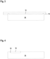
- Such a rail 13 running on an edge of the printed circuit board 10 is in figure 3 shown. How figure 3 shows, the rail 13 extends almost over the entire length of the circuit board 10. The same applies to the in figure 3 opposite rail 13, not shown.
- the longitudinal axes of the rails 13 run parallel to the edges of the printed circuit board 10, which in turn run parallel to the longitudinal axes of the grooves 12.
- the rails 13 have a rectangular Outer contour, which are adapted to the inner contours of the grooves 12, so that by pressing the rails 13 in the grooves 12 a play-free mounting of the circuit board 10 is given.
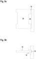
- figure 4 shows a variant of the embodiment of FIG figure 3 .
- a rail element 14 is mounted on the edge of circuit board 10 .
- the length of which is significantly less than the length of the circuit board 10.
- a plurality of rail elements 14 arranged at a distance from one another can be fastened to the edge of the circuit board 10.
- the or each rail element 14 is mounted in a recess 15 of the printed circuit board 10 in such a way that the rail element 14 protrudes slightly over the edge of the printed circuit board 10 so that it can be clamped in the respective groove 12 .
- the longitudinal axis of the or each rail element 14 runs parallel to the edge of the circuit board 10.
- the or each rail element 14 has a rectangular outer contour.
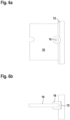
- FIG. 5a, 5b show a variant of the embodiment according to FIG figure 4 .
- the embodiment of Figures 5a, 5b differs from the embodiment according to figure 4 characterized in that the or the rail elements 14 have a wedge-shaped cross section, which causes improved clamping in the groove 12 and thereby an improved damping effect.
- wedge-shaped cross-sections can also be used with the rails 13 according to FIG figure 3 be provided.
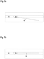
- FIGS. 6a, 6b show an embodiment in which an elastic element made of elastic material is formed by a segment of a cable hose guide 16, which is mounted on the edge of the circuit board 10.
- FIGS. 7a, 7b show a further exemplary embodiment of the mounting according to the invention of the printed circuit board 10 in the grooves 12.
- a rail element 14 is fastened to each edge of the circuit board 10 in the region of a longitudinal end of the circuit board 10, the size and arrangement on the circuit board 10 being identical for both rail elements 14.
- these rail elements 14 are fastened to the printed circuit board 10 in such a way that their longitudinal axes run obliquely, ie inclined to the edge of the printed circuit board 10.
- the widths of the rail elements 14 are slightly smaller than the width of the grooves 12, so that the rail elements 14 are guided in the respective groove 12 with little friction and with some play when the longitudinal axis of the respective rail element 14 coincides with the longitudinal axis of the groove 12.
- Figure 7a shows the insertion of the printed circuit board 10 into the area of the grooves 12.
- the printed circuit board 10 is positioned at an angle such that the longitudinal axes of the rail elements 14 guided in the grooves 12 coincide with the longitudinal axes of the grooves 12. Since the rail elements 14 are guided in the grooves 12 with little friction, the printed circuit board 10 can be easily pushed into the area of the grooves 12 .
- the printed circuit board 10 is tilted so that the printed circuit board sections 17a, 17b lie in the plane of the grooves 12, as shown in FIG Figure 7b shown.
- the rail elements 14 are inclined in the grooves 12 and are clamped in the grooves 12, such as Figure 7b shows. This position can be fixed in that the end of the circuit board 10 facing away from the rail element 14 is fastened to a housing cover.
- FIGS. 8a, 8b and 9a, 9b show a further exemplary embodiment of the mounting according to the invention of the printed circuit board 10 in the grooves 12.
- the printed circuit board 10 does not have a rectangular outer contour. Rather, the printed circuit board 10 has two printed circuit board sections 17a, 17b, which are arranged rotationally symmetrically to a fulcrum in the center of the circuit board 10, the fulcrum lying in the center plane A of the circuit board 10.
- the printed circuit board sections 17a, 17b can be shaped conically towards the longitudinal end of the printed circuit board 10 (not shown).
- a rail element 14 is mounted in a recess 15 on each of the edge segments 18a of the circuit board sections 17a, 17b arranged opposite on the circuit board 10 .
- the printed circuit board 10 is rotated about the pivot point in the plane of the grooves 12, so that only the rail elements 14 are in engagement with the grooves 12 ( figures 8b , 9b ). As a result, the circuit board 10 is fixed in position in the grooves 12 .
Landscapes
- Physics & Mathematics (AREA)
- Life Sciences & Earth Sciences (AREA)
- General Life Sciences & Earth Sciences (AREA)
- General Physics & Mathematics (AREA)
- Geophysics (AREA)
- Mounting Of Printed Circuit Boards And The Like (AREA)
Abstract
Description
- Die Erfindung betrifft einen optischen Sensor.
- Derartige optische Sensoren werden generell zur Erfassung von Objekten in einem Überwachungsbereich eingesetzt.
- In der einfachsten Ausführungsform weist der optische Sensor als Sensorkomponente nur einen Lichtstrahlen emittierenden Sender und einen Lichtstrahlen empfangenden Empfänger auf. Der optische Sensor kann dabei als Lichttaster, Distanzsensor, Reflexionslichtschranke und dergleichen ausgebildet sein, wobei bei diesen Ausführungsformen der Sender und der Empfänger in einem gemeinsamen Gehäuse integriert sind. Weiterhin kann der optische Sensor auch als Lichtschranke ausgebildet sein. In diesem Fall sind der Sender und Empfänger in separaten Gehäusen untergebracht.
- Generell kann der optische Sensor auch mehrere Sender und/oder Empfänger aufweisen. Ein Beispiel für einen derartigen optischen Sensor ist ein Lichtvorhang.
- Der Lichtvorhang umfasst typischerweise in einem ersten Gehäuse an einem Rand des Überwachungsbereichs eine Reihenanordnung von Lichtstrahlen emittierenden Sendern und in einem zweiten Gehäuse an dem gegenüberliegenden Rand des Überwachungsbereichs eine Reihenanordnung von Lichtstrahlen empfangenden Empfängern.
- Der optische Sensor weist als Elektronikkomponente eine Auswerteeinheit auf, in welcher in Abhängigkeit von Empfangssignalen des oder der Empfänger ein Objektfeststellungssignal generiert wird. Dieses Objektfeststellungssignal kann insbesondere als binäres Schaltsignal ausgebildet sein, dessen Schaltzustände angeben, ob sich ein Objekt im Überwachungsbereich befindet oder nicht. Das Objektfeststellungssignal kann alternativ ein analoges Signal, beispielsweise ein Distanzwert sein.
- Die Sensorkomponenten und die Elektronikkomponenten des optischen Sensors sind auf wenigstens einer Leiterplatte angeordnet. Die oder jede Leiterplatte ist in dem oder in einem Gehäuse des optischen Sensors untergebracht.
- Die jeweilige Leiterplatte muss exakt in einer bestimmten Sollposition gelagert werden. Dabei muss diese Sollposition auch bei äußeren Umgebungseinflüssen, wie Schwingungs- oder Schockbelastungen, erhalten bleiben. Um dies zu erreichen, werden die Leiterplatten in den jeweiligen Gehäusen mit Befestigungsmitteln fixiert. Ein Beispiel hierfür sind Schraubverbindungen.
- Diese Befestigungen erfordern den Einsatz von Werkzeugen und sind zudem zeitaufwändig.
- Der Erfindung liegt die Aufgabe zugrunde, einen optischen Sensor der eingangs genannten Art, bereitzustellen, der eine hohe Funktionalität aufweist und der rationell und kostengünstig gefertigt werden kann.
- Zur Lösung dieser Aufgabe sind die Merkmale des Anspruchs 1 vorgesehen. Vorteilhafte Ausführungsformen und zweckmäßige Weiterbildungen der Erfindung sind in den abhängigen Ansprüchen beschrieben.
- Die Erfindung betrifft einen optischer Sensor zur Erfassung von Objekten innerhalb eines Überwachungsbereichs, mit Sensorkomponenten und Elektronikkomponenten. Die Sensor- und Elektronikkomponenten sind in wenigstens einem Gehäuse angeordnet, in welchem wenigstens eine Sensorkomponenten und/oder Elektronikkomponenten aufnehmende Leiterplatte gelagert ist. Die Leiterplatte ist unter Zwischenlagerung eines elastischen Materials in im Gehäuse angeordneten Nuten spielfrei gelagert.
- Der erfindungsgemäße optische Sensor kann als Sensorkomponenten generell nur einen Sender und nur einen Empfänger aufweisen, wobei dann der optische Sensor als Lichtschranke, Reflexionslichtschranke, Lichttaster, Distanzsensor oder dergleichen ausgebildet sein kann. Der optische Sensor kann auch eine Mehrfachanordnung von Sendern und/oder Empfängern aufweisen. Insbesondere kann der optische Sensor als Lichtvorhang ausgebildet sein.
- Die Funktionsweise des optischen Sensors ist generell derart, dass der optische Sensor als Elektronikkomponente eine Auswerteeinheit aufweist, in der abhängig von Empfangssignalen des oder der Empfänger ein Objektfeststellungssignal generiert, welches angibt, ob ein Objekt im Überwachungsbereich vorhanden ist.
- Der optische Sensor kann generell als Sicherheitssensor ausgebildet sein. Für den Einsatz im Bereich der Sicherheitstechnik weist dieser einen fehlersicheren Aufbau auf, was beispielsweise durch eine zweikanalige Auswerteeinheit realisiert wird.
- Durch die erfindungsgemäße Zwischenlagerung eines elastischen Materials zwischen dem Rand der Leiterplatte und der oder jeder zugeordneten Nut wird eine positionssichere stabile Lagerung der Leiterplatte in der oder in den Nuten erhalten. Die Leiterplatte ist mittels des elastischen Materials spielfrei in den Nuten gelagert, wobei die Lagerung der Leiterplatte an ihrer Sollposition auch bei äußeren Störeinflüssen, wie Schock- oder Schwingungsbelastungen erhalten bleibt.
- Dabei ist besonders vorteilhaft, dass das elastische Material eine Schwingungs- und Schockdämpfung bewirkt.
- Dadurch werden auch auf der Leiterplatte gelagerte elektronische Bauteile gegen Schock- und Schwingungsbelastungen geschützt.
- Unempfindlichkeit gegen Schock- und Schwingungsbelastungen ist insbesondere bei als Sicherheitssensor ausgebildeten optischen Sensoren von Bedeutung, da diese strenge Anforderungen an die Unempfindlichkeit gegen derartige Belastungen erfüllen müssen.
- Ein weiterer wesentlicher Vorteil der Erfindung besteht darin, dass die Leiterplatten werkzeuglos in den jeweiligen Aufnahmen fixiert werden können. Dadurch wird eine einfache und schnelle Montage des optischen Sensors ermöglicht.
- Da die Leiterplatte unter Zwischenlagerung des elastischen Materials in den Nuten gelagert ist, entsteht auch kein Abrieb der Leiterplatte, der bei einer direkten Lagerung der Leiterplatte in den Nuten vorhanden wäre, insbesondere dann, wenn die Nuten aus metallischen Werkstoffen wie Aluminium bestehen.
- Weiter ist vorteilhaft, dass das elastische Material eine Isolierung der Leiterplatte gegenüber dem Gehäuse bewirkt.
- Gemäß einer vorteilhaften Ausführungsform ist das elastische Material ein Kunststoff.
- Dabei wird als elastisches Material ein Kunststoff gewählt, der mechanisch verformbar ist. Insbesondere ist das elastische Material ein Elastomer.
- Besonders vorteilhaft ist das elastische Material in Form von in den Nuten und/oder der Leiterplatte gelagerten elastischen Elementen ausgebildet.
- Die elastischen Elemente bilden Formteile, die an die Konturen der Nuten angepasst sind.
- Vorteilhaft sind die elastischen Elemente durch Klemm-, Rast- oder Clips-Mittel an der Leiterplatte oder an den Nuten befestigbar.
- Somit ist eine werkzeuglose Befestigungsmöglichkeit der elastischen Elemente gegeben.
- Die elastischen Elemente können unterschiedliche Geometrien und Ausdehnungen entlang der Leiterplatte aufweisen. Prinzipiell können die elastischen Elemente polygonal oder kreiszylindrisch ausgebildet sein.
- Gemäß einer besonders vorteilhaften Ausgestaltung ist an jedem in eine Nut einführbaren Rand der Leiterplatte ein elastisches Element in Form einer Schiene befestigt.
- Zweckmäßig erstreckt sich jede Schiene zumindest näherungsweise über die gesamte Länge des Randes der Leiterplatte.
- Die Außenkonturen der Schienen sind an die Innenkonturen der Nuten angepasst, wodurch eine spielfreie Lagerung der Leiterplatte in den Nuten gewährleistet ist.
- Gemäß einer weiteren vorteilhaften Ausgestaltung ist an jedem in eine Nut einführbaren Rand der Leiterplatte wenigstens ein elastisches Element in Form eines Schienenelements befestigt.
- Dabei ist die Länge des Schienenelements signifikant kleiner als die Länge des Randes der Leiterplatte.
- Auch die Schienenelemente sind an die Nutenkontur angepasst.
- Gemäß einer konstruktiv vorteilhaften Ausgestaltung ist das oder jedes Schienenelement in einer am Rand der Leiterplatte ausmündenden Aussparung gelagert.
- Damit wird ein besonders guter Halt des Schienenelements an der Leiterplatte gewährleistet. Zudem kann ein geringer Überstand des Schienenelements über den Rand der Leiterplatte realisiert werden.
- Vorteilhaft verlaufen die Nuten jeweils einer Geraden, wobei die Geraden parallel zueinander verlaufen.
- Die gegenüberliegend in einer Ebene angeordneten Nuten sorgen für einen beidseitigen Halt an gegenüberliegenden längsseitigen Rändern der Leiterplatte.
- Gemäß einer vorteilhaften Ausgestaltung verlaufen die Ränder der Leiterplatte parallel zueinander jeweils entlang einer Geraden.
- Zweckmäßig können daran angepasst die Längsachsen der Schienen parallel zu den Rändern der Leiterplatte verlaufen.
- Ebenso können die Längsachsen der Schienenelemente parallel zu den Rändern der Leiterplatte verlaufen.
- Bei diesen Konfigurationen werden die Schienen bzw. Schienenelemente in die Nuten eingeschoben, um die Leiterplatte zwischen den Nuten zu positionieren. Hierzu müssen Reibungskräfte zwischen den Schienen bzw. Schienenelemente und den Wänden der Nuten überwunden werden.
- Gemäß einer alternativen Ausführungsform ist in einem längsseitigen Endbereich der Leiterplatte an deren Rändern jeweils ein Schienenelement angeordnet, wobei die Längsachsen der Schienenelemente geneigt zu den Rändern der Leiterplatte verlaufen.
- Dabei ist zur Einführung der Leiterplatte in den Bereich der Nuten die Leiterplatte schräg gestellt, so dass die Längsachsen der in den Nuten geführten Schienenelemente parallel zu den Längsachsen der Nuten verlaufen. Zur Fixierung der Leiterplatte wird diese in einer von den Nuten aufgespannten Ebene ausgerichtet, wodurch durch Verkanten der Schienenelemente in den Nuten die Leiterplatte lagegesichert ist.
- In diesem Fall können die Außenkonturen der Schienenelemente so auf die Innenkonturen der Nuten abgestimmt sein, dass dann, wenn die Längsachsen der Schienenelemente in Richtung der Längsachsen der Nuten verlaufen, die Schienenelemente mit geringem Spiel in den Nuten geführt sind. Damit können bei Einführen der Leiterplatte in den Bereich der Nuten die Schienenelemente nahezu reibungsfrei in den Nuten geführt sein.
- Erst dann, wenn die Leiterplatte ihre Sollposition relativ zu den Nuten erreicht hat und die Leiterplatte in die Ebene der Nuten gekippt wird, verkanten die Schienenelemente in den Nuten. Durch dieses Verklemmen sind die Schienenelemente in den Nuten und damit auch die Leiterplatten lagegesichert.
- Gemäß einer weiteren alternativen Ausführungsform verjüngt sich die Breite der Leiterplatte von ihrer Mitte zu den längsseitigen Enden hin kontinuierlich.
- Somit weist die Leiterplatte zwei zu deren Mittenebene symmetrische, sich konisch zu deren längsseitigen Enden verjüngende Abschnitte auf.
- In diesem Fall ist an jedem konischen Abschnitt der Leiterplatte ein Schienenelement vorhanden, wobei die beiden Schienenelemente an gegenüberliegenden Rändern der Leiterplatte angeordnet sind.
- Dann erfolgt das Einführen der Leiterlatte in die Nuten in einer ersten seitlichen Kippstellung der Leiterplatte, in welcher die Randbereiche der Leiterplatte ohne Schienenelemente in den Nuten geführt sind.
- Anschließend wird die Leiterplatte dadurch in den Nuten lagefixiert, dass die Leiterplatte seitlich in eine zweite Kippstellung gekippt wird, in welche die Schienenelemente in Eingriff mit den Nuten sind.
- In der ersten Kippstellung sind die Schienenelemente außer Eingriff mit den Nuten. Vielmehr sind nur Leiterplatten-Abschnitte ohne Schienenelemente in den Nuten geführt. Damit kann das Einführen der Leiterplatte in den Bereich der Nuten nahezu ohne Reibungskräfte erfolgen, da die Leiterplatten-Ränder mit Spiel in den Nuten geführt sind.
- Um die Leiterplatte in ihrer Sollposition zu fixieren, muss diese nur von der ersten in die zweite Kippstellung gekippt werden. Dadurch werden die Schienenelemente in Eingriff mit den Nuten gebracht.
- Die Erfindung wird im Folgenden anhand der Zeichnungen erläutert. Es zeigen:
- Figur 1:
- Ausführungsbeispiel des erfindungsgemäßen optischen Sensors in Form eines Lichtvorhangs.
- Figur 2:
- Schnittdarstellung eines Gehäuses des Lichtvorhangs gemäß
Figur 1 mit einer Leiterplatte, die in Nuten des Gehäuses unter Zwischenlagerung eines elektrischen Materials gelagert ist. - Figur 3:
- Ausführungsbeispiel einer aus elektrischem Material bestehenden Schiene an der Leiterplatte.
- Figur 4:
- Ausführungsbeispiel eines aus elektrischem Material bestehenden Schienenelement an der Leiterplatte.
- Figur 5:
- Ausführungsbeispiel eines keilförmigen aus elektrischem Material bestehenden Schienenelement an der Leiterplatte.
- a) Draufsicht
- b) Schnittdarstellung
- Figur 6:
- Ausführungsbeispiel eines aus elektrischem Material bestehenden kreiszylindrischen Elements an der Leiterplatte.
- a) Draufsicht
- b) Schnittdarstellung
- Figur 7:
- Ausführungsbeispiel eines schräg an der Leiterplatte montierten, aus elektrischem Material bestehenden Schienenelement
- a) bei Einführen in eine Nut.
- b) nach Verklemmen in der Nut.
- Figur 8:
- Ausführungsbeispiel einer Leiterplatte mit zwei konischen Abschnitten und zwei an dieser befestigten Schienenelement
- a) bei Einführen der Leiterplatte in Nuten.
- b) nach Verklemmen der Schienenelemente in den Nuten.
- Figur 9a:
- Schnittdarstellung der Anordnung gemäß
Figur 8a . - Figur 9b:
- Schnittdarstellung der Anordnung gemäß
Figur 8b . -
Figur 1 zeigt schematisch den Aufbau eines Ausführungsbeispiels des erfindungsgemäßen optischen Sensors in Form eines Lichtvorhangs 1 zur Erfassung von Objekten innerhalb eines Überwachungsbereichs. - Der Lichtvorhang 1 weist eine Sendereinheit mit einem Gehäuse 2a mit einer Reihenanordnung von Lichtstrahlen 3 emittierenden Sendern 4 und diesen zugeordneten Optikelemente bildenden Sendeoptiken 5 auf. Weiterhin weist der Lichtvorhang 1 eine Empfängereinheit mit einem zweiten Gehäuse 2b mit einer Reihenanordnung von Lichtstrahlen 3 empfangenden Empfängern 6 auf, welchen jeweils ein Optikelement in Form einer Empfangsoptik 7 vorgeordnet ist.
- Die Gehäuse 2a, 2b sind an gegenüberliegenden Rändern des Überwachungsbereichs so angeordnet, dass jeweils ein Empfänger 6 einem Sender 4 gegenüberliegend angeordnet ist und mit diesem ein Sender-Empfänger-Paar bildet, wobei die Lichtstrahlen 3 des Senders 4 eine Strahlachse bilden. Im vorliegenden Fall sind acht Strahlachsen vorgesehen. Natürlich kann der Lichtvorhang 1 auch eine andere Zahl von Strahlachsen aufweisen.
- Alternativ kann der Lichtvorhang 1 auch als Reflexions-Lichtvorhang 1 ausgebildet sein. Dann sind alle Sender 4 und Empfänger 6 in einem Gehäuse 2a oder 2b angeordnet, welche an einem Rand des Überwachungsbereichs angeordnet ist. Am anderen Ende befindet sich ein Reflektor. Bei freiem Überwachungsbereich werden die Lichtstrahlen 3 der Sender 4 über den Reflektor zurück zum jeweils zugeordneten Empfänger 6 geführt.
- Die Sender 4 werden von einer Sendersteuerung 8 gesteuert. Den Empfängern 6 ist eine Auswerteeinheit 9 zugeordnet. Dabei werden die Strahlachsen zyklisch einzeln nacheinander aktiviert. Die Auswerteeinheit 9 steuert die Empfänger 6 an und wertet deren Empfangssignale zur Generierung eines Objektfeststellungssignals in Form eines binären Schaltsignals aus, dessen Schaltzustände angeben, ob sich ein Objekt im Überwachungsbereich befindet oder nicht. Bei freiem Überwachungsbereich gelangen die Lichtstrahlen 3 der Strahlachsen ungehindert zum Empfänger 6 der jeweiligen Strahlachse. Bei einem Objekteingriff wird wenigstens eine Strahlachse unterbrochen. Die Auswerteeinheit 9 kann einen mehrkanaligen Aufbau aufweisen, falls der Lichtvorhang 1 einen Sicherheitssensor bildet.
- Die Sender 4 und Empfänger 6 bilden Sensorkomponenten des optischen Sensors. Die Sendersteuerung 8 und die Auswerteeinheit 9 bilden Elektronikkomponenten des optischen Sensors. Die Sensorkomponenten und Elektronikkomponenten sind auf die Leiterplatte 10 angeordnet, die erfindungsgemäß in Aufnahmen der Gehäuse 2a oder 2b spielfrei gelagert sind.
-
Figur 2 zeigt eine Schnittdarstellung des Gehäuses 2b, wobei der dort gezeigte Aufbau auch im Gehäuse 2a vorhanden ist. - Die Leiterplatte 10, die im vorliegenden Fall eine rechteckige Kontur aufweist, ist so im Gehäuse 2b untergebracht, dass deren Längsachse mit der Längsachse des Gehäuses 2b zusammenfällt.
-
Figur 2 zeigt einen auf der Leiterplatte 10 angeordneten Empfänger 6, dem eine Empfangsoptik 7 vorgeordnet ist. Die Empfangsoptik 7 befindet sich hinter einer transparenten Scheibe 11, die die offene Vorderseite des Gehäuses 2b abschließt. - Als Aufnahme für die Leiterplatte 10 sind in den Seitenwänden des Gehäuses 2a oder 2b Nuten 12 vorgesehen. In jeder Seitenwand befindet sich eine Nut 12. Die identisch ausgebildeten Nuten 12 verlaufen parallel zueinander in einer horizontalen Ebene und erstrecken sich in Richtung der Längsachse des Gehäuses 2a oder 2b. Die Nuten 12 weisen eine rechteckige Kontur auf, die über die Länge der jeweiligen Nut 12 konstant ist. Diese Anordnung der Nuten 12 ist auch für alle weiteren Ausführungsbeispiele gegeben.
- Erfindungsgemäß ist die Leiterplatte 10 unter Zwischenlagerung eines elastischen Materials in den Nuten 12 gelagert. Dadurch wird eine spielfreie, schock- und schwingungsdämpfende Lagerung der Leiterplatte 10 erhalten. Zudem wird mit dem elastischen Material eine elektrisch isolierende Wirkung erzielt. Das elastische Material besteht aus einem elastisch verformbaren Kunststoff, insbesondere einem Elastomer.
- Im vorliegenden Fall besteht das elastische Material aus Schienen 13, die auf den Rändern durch Klemm-, Rast- oder Clips-Mitteln fixiert sind.
- Eine derartige, an einem Rand der Leiterplatte 10 verlaufende Schiene 13 ist in
Figur 3 dargestellt. WieFigur 3 zeigt, erstreckt sich die Schiene 13 nahezu über die gesamte Länge der Leiterplatte 10. Dasselbe gilt für die inFigur 3 nicht dargestellte gegenüberliegende Schiene 13. Die Längsachsen der Schienen 13 verlaufen parallel zu den Rändern der Leiterplatte 10, die wiederum parallel zu den Längsachsen der Nuten 12 verlaufen. Die Schienen 13 weisen eine rechteckige Außenkontur auf, die an die Innenkonturen der Nuten 12 angepasst sind, so dass durch Einpressen der Schienen 13 in die Nuten 12 eine spielfreie Lagerung der Leiterplatte 10 gegeben ist. -
Figur 4 zeigt eine Variante der Ausführungsform derFigur 3 . In diesem Fall ist ein Schienenelement 14 am Rand der Leiterplatte 10 gelagert. Dessen Länge signifikant kleiner ist als die Länge der Leiterplatte 10. Generell können mehrere in Abstand zueinander angeordnete Schienenelemente 14 am Rand der Leiterplatte 10 befestigt sein. WieFigur 4 zeigt, ist das oder jedes Schienenelement 14 in einer Aussparung 15 der Leiterplatte 10 so gelagert, dass das Schienenelement 14 etwas über den Rand der Leiterplatte 10 hervorsteht, so dass es in der jeweiligen Nut 12 festgeklemmt werden kann. Die Längsachse des oder jedes Schienenelements 14 verläuft parallel zum Rand der Leiterplatte 10. Das oder jedes Schienenelement 14 weist eine rechteckige Außenkontur auf. - Die
Figuren 5a, 5b zeigen eine Variante der Ausführungsform gemäßFigur 4 . Die Ausführungsform derFiguren 5a, 5b unterscheidet sich von der Ausführungsform gemäßFigur 4 dadurch, dass das oder die Schienenelemente 14 einen keilförmigen Querschnitt aufweisen, was eine verbesserte Klemmung in der Nut 12 und dadurch eine verbesserte Dämpfungswirkung bewirkt. Keilförmige Querschnitte können natürlich auch bei den Schienen 13 gemäßFigur 3 vorgesehen sein. - Die
Figuren 6a, 6b zeigen ein Ausführungsbeispiel, bei dem ein aus elastischem Material bestehendes elastisches Element von einem Segment einer Kabelschlauchführung 16 gebildet ist, die am Rand der Leiterplatte 10 gelagert ist. - Die
Figuren 7a, 7b zeigen ein weiteres Ausführungsbeispiel der erfindungsgemäßen Lagerung der Leiterplatte 10 in den Nuten 12. - Im Bereich eines längsseitigen Endes der Leiterplatte 10 ist an jedem Rand der Leiterplatte 10 ein Schienenelement 14 befestigt, wobei Größe und Anordnung an der Leiterplatte 10 für beide Schienenelemente 14 identisch sind.
- Wie die
Figur 7a, 7b zeigen sind diese Schienenelemente 14 so an der Leiterplatte 10 befestigt, dass deren Längsachsen schräg, d. h. geneigt zum Rand der Leiterplatte 10 verlaufen. Die Breiten der Schienenelemente 14 sind etwas kleiner als die Breite der Nuten 12, so dass die Schienenelemente 14 reibungsarm und mit etwas Spiel in der jeweiligen Nut 12 geführt sind, wenn die Längsachse des jeweiligen Schienenelements 14 mit der Längsachse der Nut 12 zusammenfällt. -
Figur 7a zeigt das Einführen der Leiterplatte 10 in den Bereich der Nuten 12. Die Leiterplatte 10 ist dabei so schräg gestellt, dass die Längsachsen der in den Nuten 12 geführten Schienenelemente 14 mit den Längsachsen der Nuten 12 zusammenfallen. Da somit die Schienenelemente 14 reibungsarm in den Nuten 12 geführt sind, kann die Leiterplatte 10 leicht in den Bereich der Nuten 12 eingeschoben werden. - Ist die Leiterplatte 10 in ihre Sollposition eingeschoben, wird die Leiterplatte 10 gekippt, so dass die Leiterplattenabschnitte 17a, 17b in der Ebene der Nuten 12 liegen, wie in
Figur 7b dargestellt. Dadurch werden die Schienenelemente 14 in den Nuten 12 schräg gestellt und werden so in den Nuten 12 festgeklemmt, wieFigur 7b zeigt. Diese Position kann dadurch fixiert werden, dass das dem Schienenelement 14 abgewandte Ende der Leiterplatte 10 an einem Gehäusedeckel befestigt wird. - Die
Figuren 8a, 8b und9a, 9b zeigen ein weiteres Ausführungsbeispiel der erfindungsgemäßen Lagerung der Leiterplatte 10 in den Nuten 12. - Bei dieser Ausführungsform weist die Leiterplatte 10 keine rechteckige Außenkontur auf. Vielmehr weist die Leiterplatte 10 zwei Leiterplattenabschnitte 17a, 17b auf, die drehsymmetrisch zu einem Drehpunkt im Zentrum der Leiterplatte 10 angeordnet sind, wobei der Drehpunkt in der Mittelebene A der Leiterplatte 10 liegt.
- Darüber hinaus können die Leiterplattenabschnitte 17a, 17b zum längsseitigen Ende der Leiterplatte 10 hin konisch geformt sein (nicht gezeigt).
- An den gegenüberliegend an der Leiterplatte 10 angeordneten Randsegmenten 18a der Leiterplattenabschnitte 17a, 17b ist jeweils ein Schienenelement 14 in einer Aussparung 15 gelagert.
- Bei Einführen der Leiterplatte 10 in den Bereich der Nuten 12 liegen nur die Randsegmente 18b ohne Schienenelemente 14 in den Nuten 12, wie in den Figuren 8a, 9a dargestellt. Da die Leiterplatte 10 mit Spiel in den Nuten 12 liegt, kann die Leiterplatte 10 reibungsarm in den Bereich der Nuten 12 eingeschoben werden.
- Zum Fixieren der Leiterplatte 10 in den Nuten 12 wird die Leiterplatte 10 in der Ebene der Nuten 12 um den Drehpunkt gedreht, so dass nur die Schienenelemente 14 im Eingriff mit den Nuten 12 sind (
Figuren 8b ,9b ). Dadurch ist die Leiterplatte 10 in den Nuten 12 lagefixiert. -
- (1)
- Lichtvorhang
- (2a)
- Gehäuse
- (2b)
- Gehäuse
- (3)
- Lichtstrahl
- (4)
- Sender
- (5)
- Sendeoptik
- (6)
- Empfänger
- (7)
- Empfangsoptik
- (8)
- Sendersteuerung
- (9)
- Auswerteeinheit
- (10)
- Leiterplatte
- (11)
- Scheibe
- (12)
- Nut
- (13)
- Schiene
- (14)
- Schienenelement
- (15)
- Aussparung
- (16)
- Kabelschlauchführung
- (17a)
- Leiterplattenabschnitt
- (17b)
- Leiterplattenabschnitt
- (18a)
- Randsegment mit Schienenelement
- (18b)
- Randsegment ohne Schienenelement
Claims (24)
- Optischer Sensor zur Erfassung von Objekten innerhalb eines Überwachungsbereichs, mit Sensorkomponenten und Elektronikkomponenten, welche in wenigstens einem Gehäuse 2a oder 2b angeordnet sind, in welchem wenigstens eine Sensorkomponenten und/oder Elektronikkomponenten aufnehmende Leiterplatte (10) gelagert ist, dadurch gekennzeichnet, dass die Leiterplatte (10) unter Zwischenlagerung eines elastischen Materials in im Gehäuse 2a oder 2b angeordneten Nuten (12) spielfrei gelagert ist.
- Optischer Sensor nach Anspruch 1, dadurch gekennzeichnet, dass das elastische Material eine Schwingungs- und Schockdämpfung bewirkt.
- Optischer Sensor nach Anspruch 1, dadurch gekennzeichnet, dass das elastische Material ein Kunststoff ist.
- Optischer Sensor nach einem der Ansprüche 1 bis 3, dadurch gekennzeichnet, dass das elastische Material ein Elastomer ist.
- Optischer Sensor nach einem der Ansprüche 1 bis 4, dadurch gekennzeichnet, dass das elastische Material eine elektrische Isolierung der Leiterplatte (10) gegenüber dem Gehäuse 2a oder 2b bewirkt.
- Optischer Sensor nach einem der Ansprüche 1 bis 5, dadurch gekennzeichnet, dass das elastische Material in Form von in den Nuten (12) und/oder der Leiterplatte (10) gelagerten elastischen Elementen ausgebildet ist.
- Optischer Sensor nach Anspruch 6, dadurch gekennzeichnet, dass die elastischen Elemente durch Klemm-, Rast- oder Clips-Mittel an der Leiterplatte (10) oder an den Nuten (12) befestigbar sind.
- Optischer Sensor nach einem der Ansprüche 6 oder 7, dadurch gekennzeichnet, dass an jedem in eine Nut (12) einführbaren Rand der Leiterplatte (10) ein elastisches Element in Form einer Schiene (13) befestigt ist.
- Optischer Sensor nach Anspruch 8, dadurch gekennzeichnet, dass sich jede Schiene (13) zumindest näherungsweise über die gesamte Länge des Randes der Leiterplatte (10) erstreckt.
- Optischer Sensor nach einem der Ansprüche 6 oder 7, dadurch gekennzeichnet, dass an jedem in eine Nut (12) einführbaren Rand der Leiterplatte (10) wenigstens ein elastisches Element in Form eines Schienenelements (14) befestigt ist.
- Optischer Sensor nach Anspruch 10, dadurch gekennzeichnet, dass die Länge des Schienenelements (14) signifikant kleiner ist als die Länge des Randes der Leiterplatte (10).
- Optischer Sensor nach einem der Ansprüche 10 oder 11, dadurch gekennzeichnet, dass das oder jedes Schienenelement (14) in einer am Rand der Leiterplatte (10) ausmündenden Aussparung (15) gelagert ist.
- Optischer Sensor nach einem der Ansprüche 1 bis 12, dadurch gekennzeichnet, dass die Nuten (12) jeweils einer Geraden verlaufen, wobei die Geraden parallel zueinander verlaufen.
- Optischer Sensor nach einem der Ansprüche 1 bis 13, dadurch gekennzeichnet, dass die Ränder der Leiterplatte (10) parallel zueinander jeweils entlang einer Geraden verlaufen.
- Optischer Sensor nach einem der Ansprüche 8 und 14, dadurch gekennzeichnet, dass die Längsachsen der Schienen (13) parallel zu den Rändern der Leiterplatte (10) verlaufen.
- Optischer Sensor nach einem der Ansprüche 10 und 14, dadurch gekennzeichnet, dass die Längsachsen der Schienenelemente (14) parallel zu den Rändern der Leiterplatte (10) verlaufen.
- Optischer Sensor nach einem der Ansprüche 10 und 14, dadurch gekennzeichnet, dass in einem längsseitigen Endbereich der Leiterplatte (10) an deren Rändern jeweils ein Schienenelement (14) angeordnet ist, wobei die Längsachsen der Schienenelemente (14) geneigt zu den Rändern der Leiterplatte (10) verlaufen.
- Optischer Sensor nach Anspruch 17, dadurch gekennzeichnet, dass zur Einführung der Leiterplatte (10) in den Bereich der Nuten (12) die Leiterplatte (10) schräg gestellt ist, so dass die Längsachsen der in den Nuten (12) geführten Schienenelemente (14) parallel zu den Längsachsen der Nuten (12) verlaufen, und dass zur Fixierung der Leiterplatte (10) diese in einer von den Nuten (12) aufgespannten Ebene ausgerichtet wird, wodurch durch Verkanten der Schienenelemente (14) in den Nuten (12) die Leiterplatte (10) lagegesichert ist.
- Optischer Sensor nach einem der Ansprüche 1 bis 13, dadurch gekennzeichnet, dass sich die Breite der Leiterplatte (10) von ihrer Mitte zu den längsseitigen Enden hin kontinuierlich verjüngt.
- Optischer Sensor nach Anspruch 19, dadurch gekennzeichnet, dass die Leiterplatte (10) zwei in deren mittelsymmetrische, sich konisch zu deren längsseitigen Enden verjüngende Abschnitte aufweist.
- Optischer Sensor nach Anspruch 20, dadurch gekennzeichnet, dass an jedem konischen Abschnitt der Leiterplatte (10) ein Schienenelement (14) vorhanden ist, wobei die beiden Schienenelemente (14) an gegenüberliegenden Rändern der Leiterplatte (10) angeordnet sind.
- Optischer Sensor nach Anspruch 21, dadurch gekennzeichnet, dass Einführen der Leiterplatte (10) in die Nuten (12) in einer ersten seitlichen Kippstellung der Leiterplatte (10) erfolgt, in welcher die Randbereiche der Leiterplatte (10) ohne Schienenelemente (14) in den Nuten (12) geführt sind.
- Optischer Sensor nach Anspruch 22, dadurch gekennzeichnet, dass die Leiterplatte (10) dadurch in den Nuten (12) lagefixiert wird, dass die Leiterplatte (10) seitlich in eine zweite Kippstellung gekippt wird, in welche die Schienenelemente (14) in Eingriff mit den Nuten (12) sind.
- Optischer Sensor nach einem der Ansprüche 1 bis 23, dadurch gekennzeichnet, dass dieser ein Sicherheitssensor ist.
Priority Applications (1)
| Application Number | Priority Date | Filing Date | Title |
|---|---|---|---|
| EP22152805.2A EP4215952B1 (de) | 2022-01-21 | 2022-01-21 | Optischer sensor |
Applications Claiming Priority (1)
| Application Number | Priority Date | Filing Date | Title |
|---|---|---|---|
| EP22152805.2A EP4215952B1 (de) | 2022-01-21 | 2022-01-21 | Optischer sensor |
Publications (2)
| Publication Number | Publication Date |
|---|---|
| EP4215952A1 true EP4215952A1 (de) | 2023-07-26 |
| EP4215952B1 EP4215952B1 (de) | 2024-05-29 |
Family
ID=79927120
Family Applications (1)
| Application Number | Title | Priority Date | Filing Date |
|---|---|---|---|
| EP22152805.2A Active EP4215952B1 (de) | 2022-01-21 | 2022-01-21 | Optischer sensor |
Country Status (1)
| Country | Link |
|---|---|
| EP (1) | EP4215952B1 (de) |
Citations (4)
| Publication number | Priority date | Publication date | Assignee | Title |
|---|---|---|---|---|
| JP2854605B2 (ja) * | 1989-06-26 | 1999-02-03 | 株式会社アイセンス | 光電センサ |
| US20070212061A1 (en) * | 2006-03-10 | 2007-09-13 | Jae Kun Woo | Camera Module and Method of Manufacturing The same |
| US20080204229A1 (en) * | 2004-11-15 | 2008-08-28 | Memco Limited | Safety Sensing System for a Powered Door System |
| CN108649944A (zh) * | 2018-05-28 | 2018-10-12 | 佛山市鑫敏电子科技有限公司 | 一种触摸感应装置 |
-
2022
- 2022-01-21 EP EP22152805.2A patent/EP4215952B1/de active Active
Patent Citations (4)
| Publication number | Priority date | Publication date | Assignee | Title |
|---|---|---|---|---|
| JP2854605B2 (ja) * | 1989-06-26 | 1999-02-03 | 株式会社アイセンス | 光電センサ |
| US20080204229A1 (en) * | 2004-11-15 | 2008-08-28 | Memco Limited | Safety Sensing System for a Powered Door System |
| US20070212061A1 (en) * | 2006-03-10 | 2007-09-13 | Jae Kun Woo | Camera Module and Method of Manufacturing The same |
| CN108649944A (zh) * | 2018-05-28 | 2018-10-12 | 佛山市鑫敏电子科技有限公司 | 一种触摸感应装置 |
Also Published As
| Publication number | Publication date |
|---|---|
| EP4215952B1 (de) | 2024-05-29 |
Similar Documents
| Publication | Publication Date | Title |
|---|---|---|
| EP0456187A1 (de) | Verbindung zwischen einem Träger und einem Plattenelement | |
| EP2090906B1 (de) | Optischer sensor | |
| EP0928504B1 (de) | Kontaktorgan mit doppel-schneidklemmanschluss | |
| EP0838985B1 (de) | Kontaktelement zur elektrischen Kontaktierung von Leiterkarten mit einer vorderen Modulschiene eines Baugruppenträgers | |
| DE3829109A1 (de) | Elektrischer schalter, insbesondere lenstockschalter fuer kratfahrzeuge | |
| EP4215952B1 (de) | Optischer sensor | |
| EP2393097B1 (de) | Schalter mit selbstjustierender Schaltstößelführung | |
| DE4434011C1 (de) | Optoelektronische Vorrichtung | |
| EP0355201B1 (de) | Anzeigeinstrument | |
| EP0148334B1 (de) | Anordnung zur Halterung von Zubehör an einer Leuchtenwand | |
| DE4429984C1 (de) | Elektrisches oder elektronisches Gerät für ein Kraftfahrzeug | |
| EP1653200B1 (de) | Optischer Sensor | |
| DE29620422U1 (de) | Optoelektronischer Sensor mit in einem Gehäusegrundkörper integrierten Haltevorrichtungen | |
| DE20111588U1 (de) | Befestigungsvorrichtung für einen otpischen Sensor | |
| EP0886873B1 (de) | Positionssensor | |
| EP4215935B1 (de) | Optischer sensor | |
| DE4108175C2 (de) | Befestigungsvorrichtung | |
| EP4220239A1 (de) | Optischer sensor | |
| EP4506735B1 (de) | Lichtvorhang | |
| DE10008269C2 (de) | Halterung für ein focussierendes Bauteil sowie Gehäuse für einen Radarsensor | |
| DE102004031082B4 (de) | Befestigungsmittel für einen optischen Sensor | |
| DE29916849U1 (de) | Befestigungsvorrichtung | |
| EP2069843A1 (de) | Stecksystem zum ankoppeln mindestens einer optischen faser | |
| EP1376067A1 (de) | Vorrichtung zur Befestigung eines Sensors in einer Nut | |
| DE29812609U1 (de) | Befestigungssystem |
Legal Events
| Date | Code | Title | Description |
|---|---|---|---|
| PUAI | Public reference made under article 153(3) epc to a published international application that has entered the european phase |
Free format text: ORIGINAL CODE: 0009012 |
|
| STAA | Information on the status of an ep patent application or granted ep patent |
Free format text: STATUS: REQUEST FOR EXAMINATION WAS MADE |
|
| 17P | Request for examination filed |
Effective date: 20220816 |
|
| AK | Designated contracting states |
Kind code of ref document: A1 Designated state(s): AL AT BE BG CH CY CZ DE DK EE ES FI FR GB GR HR HU IE IS IT LI LT LU LV MC MK MT NL NO PL PT RO RS SE SI SK SM TR |
|
| GRAP | Despatch of communication of intention to grant a patent |
Free format text: ORIGINAL CODE: EPIDOSNIGR1 |
|
| STAA | Information on the status of an ep patent application or granted ep patent |
Free format text: STATUS: GRANT OF PATENT IS INTENDED |
|
| RIC1 | Information provided on ipc code assigned before grant |
Ipc: G01V 8/20 20060101ALN20240305BHEP Ipc: G01V 8/14 20060101ALN20240305BHEP Ipc: G01V 8/12 20060101ALN20240305BHEP Ipc: G01V 8/10 20060101AFI20240305BHEP |
|
| GRAS | Grant fee paid |
Free format text: ORIGINAL CODE: EPIDOSNIGR3 |
|
| INTG | Intention to grant announced |
Effective date: 20240402 |
|
| RIC1 | Information provided on ipc code assigned before grant |
Ipc: G01V 8/20 20060101ALN20240315BHEP Ipc: G01V 8/14 20060101ALN20240315BHEP Ipc: G01V 8/12 20060101ALN20240315BHEP Ipc: G01V 8/10 20060101AFI20240315BHEP |
|
| GRAA | (expected) grant |
Free format text: ORIGINAL CODE: 0009210 |
|
| STAA | Information on the status of an ep patent application or granted ep patent |
Free format text: STATUS: THE PATENT HAS BEEN GRANTED |
|
| AK | Designated contracting states |
Kind code of ref document: B1 Designated state(s): AL AT BE BG CH CY CZ DE DK EE ES FI FR GB GR HR HU IE IS IT LI LT LU LV MC MK MT NL NO PL PT RO RS SE SI SK SM TR |
|
| REG | Reference to a national code |
Ref country code: CH Ref legal event code: EP |
|
| REG | Reference to a national code |
Ref country code: IE Ref legal event code: FG4D Free format text: LANGUAGE OF EP DOCUMENT: GERMAN |
|
| REG | Reference to a national code |
Ref country code: DE Ref legal event code: R096 Ref document number: 502022000938 Country of ref document: DE |
|
| P01 | Opt-out of the competence of the unified patent court (upc) registered |
Free format text: CASE NUMBER: APP_35270/2024 Effective date: 20240612 |
|
| REG | Reference to a national code |
Ref country code: LT Ref legal event code: MG9D |
|
| REG | Reference to a national code |
Ref country code: NL Ref legal event code: MP Effective date: 20240529 |
|
| PG25 | Lapsed in a contracting state [announced via postgrant information from national office to epo] |
Ref country code: IS Free format text: LAPSE BECAUSE OF FAILURE TO SUBMIT A TRANSLATION OF THE DESCRIPTION OR TO PAY THE FEE WITHIN THE PRESCRIBED TIME-LIMIT Effective date: 20240929 |
|
| PG25 | Lapsed in a contracting state [announced via postgrant information from national office to epo] |
Ref country code: BG Free format text: LAPSE BECAUSE OF FAILURE TO SUBMIT A TRANSLATION OF THE DESCRIPTION OR TO PAY THE FEE WITHIN THE PRESCRIBED TIME-LIMIT Effective date: 20240529 |
|
| PG25 | Lapsed in a contracting state [announced via postgrant information from national office to epo] |
Ref country code: HR Free format text: LAPSE BECAUSE OF FAILURE TO SUBMIT A TRANSLATION OF THE DESCRIPTION OR TO PAY THE FEE WITHIN THE PRESCRIBED TIME-LIMIT Effective date: 20240529 Ref country code: FI Free format text: LAPSE BECAUSE OF FAILURE TO SUBMIT A TRANSLATION OF THE DESCRIPTION OR TO PAY THE FEE WITHIN THE PRESCRIBED TIME-LIMIT Effective date: 20240529 |
|
| PG25 | Lapsed in a contracting state [announced via postgrant information from national office to epo] |
Ref country code: GR Free format text: LAPSE BECAUSE OF FAILURE TO SUBMIT A TRANSLATION OF THE DESCRIPTION OR TO PAY THE FEE WITHIN THE PRESCRIBED TIME-LIMIT Effective date: 20240830 |
|
| PG25 | Lapsed in a contracting state [announced via postgrant information from national office to epo] |
Ref country code: ES Free format text: LAPSE BECAUSE OF FAILURE TO SUBMIT A TRANSLATION OF THE DESCRIPTION OR TO PAY THE FEE WITHIN THE PRESCRIBED TIME-LIMIT Effective date: 20240529 |
|
| PG25 | Lapsed in a contracting state [announced via postgrant information from national office to epo] |
Ref country code: PL Free format text: LAPSE BECAUSE OF FAILURE TO SUBMIT A TRANSLATION OF THE DESCRIPTION OR TO PAY THE FEE WITHIN THE PRESCRIBED TIME-LIMIT Effective date: 20240529 |
|
| PG25 | Lapsed in a contracting state [announced via postgrant information from national office to epo] |
Ref country code: LV Free format text: LAPSE BECAUSE OF FAILURE TO SUBMIT A TRANSLATION OF THE DESCRIPTION OR TO PAY THE FEE WITHIN THE PRESCRIBED TIME-LIMIT Effective date: 20240529 |
|
| PG25 | Lapsed in a contracting state [announced via postgrant information from national office to epo] |
Ref country code: PL Free format text: LAPSE BECAUSE OF FAILURE TO SUBMIT A TRANSLATION OF THE DESCRIPTION OR TO PAY THE FEE WITHIN THE PRESCRIBED TIME-LIMIT Effective date: 20240529 Ref country code: NO Free format text: LAPSE BECAUSE OF FAILURE TO SUBMIT A TRANSLATION OF THE DESCRIPTION OR TO PAY THE FEE WITHIN THE PRESCRIBED TIME-LIMIT Effective date: 20240829 Ref country code: LV Free format text: LAPSE BECAUSE OF FAILURE TO SUBMIT A TRANSLATION OF THE DESCRIPTION OR TO PAY THE FEE WITHIN THE PRESCRIBED TIME-LIMIT Effective date: 20240529 Ref country code: IS Free format text: LAPSE BECAUSE OF FAILURE TO SUBMIT A TRANSLATION OF THE DESCRIPTION OR TO PAY THE FEE WITHIN THE PRESCRIBED TIME-LIMIT Effective date: 20240929 Ref country code: HR Free format text: LAPSE BECAUSE OF FAILURE TO SUBMIT A TRANSLATION OF THE DESCRIPTION OR TO PAY THE FEE WITHIN THE PRESCRIBED TIME-LIMIT Effective date: 20240529 Ref country code: GR Free format text: LAPSE BECAUSE OF FAILURE TO SUBMIT A TRANSLATION OF THE DESCRIPTION OR TO PAY THE FEE WITHIN THE PRESCRIBED TIME-LIMIT Effective date: 20240830 Ref country code: FI Free format text: LAPSE BECAUSE OF FAILURE TO SUBMIT A TRANSLATION OF THE DESCRIPTION OR TO PAY THE FEE WITHIN THE PRESCRIBED TIME-LIMIT Effective date: 20240529 Ref country code: ES Free format text: LAPSE BECAUSE OF FAILURE TO SUBMIT A TRANSLATION OF THE DESCRIPTION OR TO PAY THE FEE WITHIN THE PRESCRIBED TIME-LIMIT Effective date: 20240529 Ref country code: BG Free format text: LAPSE BECAUSE OF FAILURE TO SUBMIT A TRANSLATION OF THE DESCRIPTION OR TO PAY THE FEE WITHIN THE PRESCRIBED TIME-LIMIT Effective date: 20240529 Ref country code: RS Free format text: LAPSE BECAUSE OF FAILURE TO SUBMIT A TRANSLATION OF THE DESCRIPTION OR TO PAY THE FEE WITHIN THE PRESCRIBED TIME-LIMIT Effective date: 20240829 |
|
| PG25 | Lapsed in a contracting state [announced via postgrant information from national office to epo] |
Ref country code: NL Free format text: LAPSE BECAUSE OF FAILURE TO SUBMIT A TRANSLATION OF THE DESCRIPTION OR TO PAY THE FEE WITHIN THE PRESCRIBED TIME-LIMIT Effective date: 20240529 |
|
| PG25 | Lapsed in a contracting state [announced via postgrant information from national office to epo] |
Ref country code: NL Free format text: LAPSE BECAUSE OF FAILURE TO SUBMIT A TRANSLATION OF THE DESCRIPTION OR TO PAY THE FEE WITHIN THE PRESCRIBED TIME-LIMIT Effective date: 20240529 |
|
| PG25 | Lapsed in a contracting state [announced via postgrant information from national office to epo] |
Ref country code: DK Free format text: LAPSE BECAUSE OF FAILURE TO SUBMIT A TRANSLATION OF THE DESCRIPTION OR TO PAY THE FEE WITHIN THE PRESCRIBED TIME-LIMIT Effective date: 20240529 |
|
| PG25 | Lapsed in a contracting state [announced via postgrant information from national office to epo] |
Ref country code: EE Free format text: LAPSE BECAUSE OF FAILURE TO SUBMIT A TRANSLATION OF THE DESCRIPTION OR TO PAY THE FEE WITHIN THE PRESCRIBED TIME-LIMIT Effective date: 20240529 |
|
| PG25 | Lapsed in a contracting state [announced via postgrant information from national office to epo] |
Ref country code: CZ Free format text: LAPSE BECAUSE OF FAILURE TO SUBMIT A TRANSLATION OF THE DESCRIPTION OR TO PAY THE FEE WITHIN THE PRESCRIBED TIME-LIMIT Effective date: 20240529 |
|
| PG25 | Lapsed in a contracting state [announced via postgrant information from national office to epo] |
Ref country code: SK Free format text: LAPSE BECAUSE OF FAILURE TO SUBMIT A TRANSLATION OF THE DESCRIPTION OR TO PAY THE FEE WITHIN THE PRESCRIBED TIME-LIMIT Effective date: 20240529 Ref country code: RO Free format text: LAPSE BECAUSE OF FAILURE TO SUBMIT A TRANSLATION OF THE DESCRIPTION OR TO PAY THE FEE WITHIN THE PRESCRIBED TIME-LIMIT Effective date: 20240529 |
|
| PG25 | Lapsed in a contracting state [announced via postgrant information from national office to epo] |
Ref country code: SM Free format text: LAPSE BECAUSE OF FAILURE TO SUBMIT A TRANSLATION OF THE DESCRIPTION OR TO PAY THE FEE WITHIN THE PRESCRIBED TIME-LIMIT Effective date: 20240529 |
|
| PG25 | Lapsed in a contracting state [announced via postgrant information from national office to epo] |
Ref country code: SM Free format text: LAPSE BECAUSE OF FAILURE TO SUBMIT A TRANSLATION OF THE DESCRIPTION OR TO PAY THE FEE WITHIN THE PRESCRIBED TIME-LIMIT Effective date: 20240529 Ref country code: SK Free format text: LAPSE BECAUSE OF FAILURE TO SUBMIT A TRANSLATION OF THE DESCRIPTION OR TO PAY THE FEE WITHIN THE PRESCRIBED TIME-LIMIT Effective date: 20240529 Ref country code: RO Free format text: LAPSE BECAUSE OF FAILURE TO SUBMIT A TRANSLATION OF THE DESCRIPTION OR TO PAY THE FEE WITHIN THE PRESCRIBED TIME-LIMIT Effective date: 20240529 Ref country code: EE Free format text: LAPSE BECAUSE OF FAILURE TO SUBMIT A TRANSLATION OF THE DESCRIPTION OR TO PAY THE FEE WITHIN THE PRESCRIBED TIME-LIMIT Effective date: 20240529 Ref country code: DK Free format text: LAPSE BECAUSE OF FAILURE TO SUBMIT A TRANSLATION OF THE DESCRIPTION OR TO PAY THE FEE WITHIN THE PRESCRIBED TIME-LIMIT Effective date: 20240529 Ref country code: CZ Free format text: LAPSE BECAUSE OF FAILURE TO SUBMIT A TRANSLATION OF THE DESCRIPTION OR TO PAY THE FEE WITHIN THE PRESCRIBED TIME-LIMIT Effective date: 20240529 |
|
| PG25 | Lapsed in a contracting state [announced via postgrant information from national office to epo] |
Ref country code: IT Free format text: LAPSE BECAUSE OF FAILURE TO SUBMIT A TRANSLATION OF THE DESCRIPTION OR TO PAY THE FEE WITHIN THE PRESCRIBED TIME-LIMIT Effective date: 20240529 |
|
| REG | Reference to a national code |
Ref country code: DE Ref legal event code: R097 Ref document number: 502022000938 Country of ref document: DE |
|
| PLBE | No opposition filed within time limit |
Free format text: ORIGINAL CODE: 0009261 |
|
| STAA | Information on the status of an ep patent application or granted ep patent |
Free format text: STATUS: NO OPPOSITION FILED WITHIN TIME LIMIT |
|
| PG25 | Lapsed in a contracting state [announced via postgrant information from national office to epo] |
Ref country code: SI Free format text: LAPSE BECAUSE OF FAILURE TO SUBMIT A TRANSLATION OF THE DESCRIPTION OR TO PAY THE FEE WITHIN THE PRESCRIBED TIME-LIMIT Effective date: 20240529 |
|
| 26N | No opposition filed |
Effective date: 20250303 |
|
| REG | Reference to a national code |
Ref country code: CH Ref legal event code: PL |
|
| PG25 | Lapsed in a contracting state [announced via postgrant information from national office to epo] |
Ref country code: SE Free format text: LAPSE BECAUSE OF FAILURE TO SUBMIT A TRANSLATION OF THE DESCRIPTION OR TO PAY THE FEE WITHIN THE PRESCRIBED TIME-LIMIT Effective date: 20240529 |
|
| PG25 | Lapsed in a contracting state [announced via postgrant information from national office to epo] |
Ref country code: LU Free format text: LAPSE BECAUSE OF NON-PAYMENT OF DUE FEES Effective date: 20250121 Ref country code: MC Free format text: LAPSE BECAUSE OF FAILURE TO SUBMIT A TRANSLATION OF THE DESCRIPTION OR TO PAY THE FEE WITHIN THE PRESCRIBED TIME-LIMIT Effective date: 20240529 |
|
| PG25 | Lapsed in a contracting state [announced via postgrant information from national office to epo] |
Ref country code: BE Free format text: LAPSE BECAUSE OF NON-PAYMENT OF DUE FEES Effective date: 20250131 |
|
| PG25 | Lapsed in a contracting state [announced via postgrant information from national office to epo] |
Ref country code: FR Free format text: LAPSE BECAUSE OF NON-PAYMENT OF DUE FEES Effective date: 20250131 |
|
| PG25 | Lapsed in a contracting state [announced via postgrant information from national office to epo] |
Ref country code: CH Free format text: LAPSE BECAUSE OF NON-PAYMENT OF DUE FEES Effective date: 20250131 |
|
| REG | Reference to a national code |
Ref country code: BE Ref legal event code: MM Effective date: 20250131 |
|
| PG25 | Lapsed in a contracting state [announced via postgrant information from national office to epo] |
Ref country code: IE Free format text: LAPSE BECAUSE OF NON-PAYMENT OF DUE FEES Effective date: 20250121 |
|
| PGFP | Annual fee paid to national office [announced via postgrant information from national office to epo] |
Ref country code: DE Payment date: 20260121 Year of fee payment: 5 |
|
| PGFP | Annual fee paid to national office [announced via postgrant information from national office to epo] |
Ref country code: AT Payment date: 20260301 Year of fee payment: 5 |