EP4215508A1 - Substrate and method for producing a substrate - Google Patents
Substrate and method for producing a substrate Download PDFInfo
- Publication number
- EP4215508A1 EP4215508A1 EP22152962.1A EP22152962A EP4215508A1 EP 4215508 A1 EP4215508 A1 EP 4215508A1 EP 22152962 A EP22152962 A EP 22152962A EP 4215508 A1 EP4215508 A1 EP 4215508A1
- Authority
- EP
- European Patent Office
- Prior art keywords
- layer
- dielectric insulation
- metallic
- connection
- metallic layer
- Prior art date
- Legal status (The legal status is an assumption and is not a legal conclusion. Google has not performed a legal analysis and makes no representation as to the accuracy of the status listed.)
- Pending
Links
Images

Classifications
-
- C—CHEMISTRY; METALLURGY
- C04—CEMENTS; CONCRETE; ARTIFICIAL STONE; CERAMICS; REFRACTORIES
- C04B—LIME, MAGNESIA; SLAG; CEMENTS; COMPOSITIONS THEREOF, e.g. MORTARS, CONCRETE OR LIKE BUILDING MATERIALS; ARTIFICIAL STONE; CERAMICS; REFRACTORIES; TREATMENT OF NATURAL STONE
- C04B37/00—Joining burned ceramic articles with other burned ceramic articles or other articles by heating
- C04B37/02—Joining burned ceramic articles with other burned ceramic articles or other articles by heating with metallic articles
- C04B37/023—Joining burned ceramic articles with other burned ceramic articles or other articles by heating with metallic articles characterised by the interlayer used
- C04B37/025—Joining burned ceramic articles with other burned ceramic articles or other articles by heating with metallic articles characterised by the interlayer used consisting of glass or ceramic material
-
- C—CHEMISTRY; METALLURGY
- C04—CEMENTS; CONCRETE; ARTIFICIAL STONE; CERAMICS; REFRACTORIES
- C04B—LIME, MAGNESIA; SLAG; CEMENTS; COMPOSITIONS THEREOF, e.g. MORTARS, CONCRETE OR LIKE BUILDING MATERIALS; ARTIFICIAL STONE; CERAMICS; REFRACTORIES; TREATMENT OF NATURAL STONE
- C04B37/00—Joining burned ceramic articles with other burned ceramic articles or other articles by heating
- C04B37/02—Joining burned ceramic articles with other burned ceramic articles or other articles by heating with metallic articles
- C04B37/023—Joining burned ceramic articles with other burned ceramic articles or other articles by heating with metallic articles characterised by the interlayer used
- C04B37/026—Joining burned ceramic articles with other burned ceramic articles or other articles by heating with metallic articles characterised by the interlayer used consisting of metals or metal salts
-
- C—CHEMISTRY; METALLURGY
- C04—CEMENTS; CONCRETE; ARTIFICIAL STONE; CERAMICS; REFRACTORIES
- C04B—LIME, MAGNESIA; SLAG; CEMENTS; COMPOSITIONS THEREOF, e.g. MORTARS, CONCRETE OR LIKE BUILDING MATERIALS; ARTIFICIAL STONE; CERAMICS; REFRACTORIES; TREATMENT OF NATURAL STONE
- C04B2237/00—Aspects relating to ceramic laminates or to joining of ceramic articles with other articles by heating
- C04B2237/02—Aspects relating to interlayers, e.g. used to join ceramic articles with other articles by heating
- C04B2237/04—Ceramic interlayers
- C04B2237/06—Oxidic interlayers
-
- C—CHEMISTRY; METALLURGY
- C04—CEMENTS; CONCRETE; ARTIFICIAL STONE; CERAMICS; REFRACTORIES
- C04B—LIME, MAGNESIA; SLAG; CEMENTS; COMPOSITIONS THEREOF, e.g. MORTARS, CONCRETE OR LIKE BUILDING MATERIALS; ARTIFICIAL STONE; CERAMICS; REFRACTORIES; TREATMENT OF NATURAL STONE
- C04B2237/00—Aspects relating to ceramic laminates or to joining of ceramic articles with other articles by heating
- C04B2237/02—Aspects relating to interlayers, e.g. used to join ceramic articles with other articles by heating
- C04B2237/10—Glass interlayers, e.g. frit or flux
-
- C—CHEMISTRY; METALLURGY
- C04—CEMENTS; CONCRETE; ARTIFICIAL STONE; CERAMICS; REFRACTORIES
- C04B—LIME, MAGNESIA; SLAG; CEMENTS; COMPOSITIONS THEREOF, e.g. MORTARS, CONCRETE OR LIKE BUILDING MATERIALS; ARTIFICIAL STONE; CERAMICS; REFRACTORIES; TREATMENT OF NATURAL STONE
- C04B2237/00—Aspects relating to ceramic laminates or to joining of ceramic articles with other articles by heating
- C04B2237/02—Aspects relating to interlayers, e.g. used to join ceramic articles with other articles by heating
- C04B2237/12—Metallic interlayers
-
- C—CHEMISTRY; METALLURGY
- C04—CEMENTS; CONCRETE; ARTIFICIAL STONE; CERAMICS; REFRACTORIES
- C04B—LIME, MAGNESIA; SLAG; CEMENTS; COMPOSITIONS THEREOF, e.g. MORTARS, CONCRETE OR LIKE BUILDING MATERIALS; ARTIFICIAL STONE; CERAMICS; REFRACTORIES; TREATMENT OF NATURAL STONE
- C04B2237/00—Aspects relating to ceramic laminates or to joining of ceramic articles with other articles by heating
- C04B2237/30—Composition of layers of ceramic laminates or of ceramic or metallic articles to be joined by heating, e.g. Si substrates
- C04B2237/32—Ceramic
- C04B2237/34—Oxidic
-
- C—CHEMISTRY; METALLURGY
- C04—CEMENTS; CONCRETE; ARTIFICIAL STONE; CERAMICS; REFRACTORIES
- C04B—LIME, MAGNESIA; SLAG; CEMENTS; COMPOSITIONS THEREOF, e.g. MORTARS, CONCRETE OR LIKE BUILDING MATERIALS; ARTIFICIAL STONE; CERAMICS; REFRACTORIES; TREATMENT OF NATURAL STONE
- C04B2237/00—Aspects relating to ceramic laminates or to joining of ceramic articles with other articles by heating
- C04B2237/30—Composition of layers of ceramic laminates or of ceramic or metallic articles to be joined by heating, e.g. Si substrates
- C04B2237/32—Ceramic
- C04B2237/34—Oxidic
- C04B2237/343—Alumina or aluminates
-
- C—CHEMISTRY; METALLURGY
- C04—CEMENTS; CONCRETE; ARTIFICIAL STONE; CERAMICS; REFRACTORIES
- C04B—LIME, MAGNESIA; SLAG; CEMENTS; COMPOSITIONS THEREOF, e.g. MORTARS, CONCRETE OR LIKE BUILDING MATERIALS; ARTIFICIAL STONE; CERAMICS; REFRACTORIES; TREATMENT OF NATURAL STONE
- C04B2237/00—Aspects relating to ceramic laminates or to joining of ceramic articles with other articles by heating
- C04B2237/30—Composition of layers of ceramic laminates or of ceramic or metallic articles to be joined by heating, e.g. Si substrates
- C04B2237/32—Ceramic
- C04B2237/36—Non-oxidic
- C04B2237/365—Silicon carbide
-
- C—CHEMISTRY; METALLURGY
- C04—CEMENTS; CONCRETE; ARTIFICIAL STONE; CERAMICS; REFRACTORIES
- C04B—LIME, MAGNESIA; SLAG; CEMENTS; COMPOSITIONS THEREOF, e.g. MORTARS, CONCRETE OR LIKE BUILDING MATERIALS; ARTIFICIAL STONE; CERAMICS; REFRACTORIES; TREATMENT OF NATURAL STONE
- C04B2237/00—Aspects relating to ceramic laminates or to joining of ceramic articles with other articles by heating
- C04B2237/30—Composition of layers of ceramic laminates or of ceramic or metallic articles to be joined by heating, e.g. Si substrates
- C04B2237/32—Ceramic
- C04B2237/36—Non-oxidic
- C04B2237/366—Aluminium nitride
-
- C—CHEMISTRY; METALLURGY
- C04—CEMENTS; CONCRETE; ARTIFICIAL STONE; CERAMICS; REFRACTORIES
- C04B—LIME, MAGNESIA; SLAG; CEMENTS; COMPOSITIONS THEREOF, e.g. MORTARS, CONCRETE OR LIKE BUILDING MATERIALS; ARTIFICIAL STONE; CERAMICS; REFRACTORIES; TREATMENT OF NATURAL STONE
- C04B2237/00—Aspects relating to ceramic laminates or to joining of ceramic articles with other articles by heating
- C04B2237/30—Composition of layers of ceramic laminates or of ceramic or metallic articles to be joined by heating, e.g. Si substrates
- C04B2237/32—Ceramic
- C04B2237/36—Non-oxidic
- C04B2237/368—Silicon nitride
-
- C—CHEMISTRY; METALLURGY
- C04—CEMENTS; CONCRETE; ARTIFICIAL STONE; CERAMICS; REFRACTORIES
- C04B—LIME, MAGNESIA; SLAG; CEMENTS; COMPOSITIONS THEREOF, e.g. MORTARS, CONCRETE OR LIKE BUILDING MATERIALS; ARTIFICIAL STONE; CERAMICS; REFRACTORIES; TREATMENT OF NATURAL STONE
- C04B2237/00—Aspects relating to ceramic laminates or to joining of ceramic articles with other articles by heating
- C04B2237/30—Composition of layers of ceramic laminates or of ceramic or metallic articles to be joined by heating, e.g. Si substrates
- C04B2237/40—Metallic
- C04B2237/402—Aluminium
-
- C—CHEMISTRY; METALLURGY
- C04—CEMENTS; CONCRETE; ARTIFICIAL STONE; CERAMICS; REFRACTORIES
- C04B—LIME, MAGNESIA; SLAG; CEMENTS; COMPOSITIONS THEREOF, e.g. MORTARS, CONCRETE OR LIKE BUILDING MATERIALS; ARTIFICIAL STONE; CERAMICS; REFRACTORIES; TREATMENT OF NATURAL STONE
- C04B2237/00—Aspects relating to ceramic laminates or to joining of ceramic articles with other articles by heating
- C04B2237/30—Composition of layers of ceramic laminates or of ceramic or metallic articles to be joined by heating, e.g. Si substrates
- C04B2237/40—Metallic
- C04B2237/407—Copper
-
- C—CHEMISTRY; METALLURGY
- C04—CEMENTS; CONCRETE; ARTIFICIAL STONE; CERAMICS; REFRACTORIES
- C04B—LIME, MAGNESIA; SLAG; CEMENTS; COMPOSITIONS THEREOF, e.g. MORTARS, CONCRETE OR LIKE BUILDING MATERIALS; ARTIFICIAL STONE; CERAMICS; REFRACTORIES; TREATMENT OF NATURAL STONE
- C04B2237/00—Aspects relating to ceramic laminates or to joining of ceramic articles with other articles by heating
- C04B2237/50—Processing aspects relating to ceramic laminates or to the joining of ceramic articles with other articles by heating
- C04B2237/82—Two substrates not completely covering each other, e.g. two plates in a staggered position
-
- C—CHEMISTRY; METALLURGY
- C04—CEMENTS; CONCRETE; ARTIFICIAL STONE; CERAMICS; REFRACTORIES
- C04B—LIME, MAGNESIA; SLAG; CEMENTS; COMPOSITIONS THEREOF, e.g. MORTARS, CONCRETE OR LIKE BUILDING MATERIALS; ARTIFICIAL STONE; CERAMICS; REFRACTORIES; TREATMENT OF NATURAL STONE
- C04B2237/00—Aspects relating to ceramic laminates or to joining of ceramic articles with other articles by heating
- C04B2237/50—Processing aspects relating to ceramic laminates or to the joining of ceramic articles with other articles by heating
- C04B2237/88—Joining of two substrates, where a substantial part of the joining material is present outside of the joint, leading to an outside joining of the joint
-
- H—ELECTRICITY
- H10—SEMICONDUCTOR DEVICES; ELECTRIC SOLID-STATE DEVICES NOT OTHERWISE PROVIDED FOR
- H10W—GENERIC PACKAGES, INTERCONNECTIONS, CONNECTORS OR OTHER CONSTRUCTIONAL DETAILS OF DEVICES COVERED BY CLASS H10
- H10W72/00—Interconnections or connectors in packages
- H10W72/50—Bond wires
- H10W72/531—Shapes of wire connectors
- H10W72/5363—Shapes of wire connectors the connected ends being wedge-shaped
-
- H—ELECTRICITY
- H10—SEMICONDUCTOR DEVICES; ELECTRIC SOLID-STATE DEVICES NOT OTHERWISE PROVIDED FOR
- H10W—GENERIC PACKAGES, INTERCONNECTIONS, CONNECTORS OR OTHER CONSTRUCTIONAL DETAILS OF DEVICES COVERED BY CLASS H10
- H10W72/00—Interconnections or connectors in packages
- H10W72/851—Dispositions of multiple connectors or interconnections
- H10W72/874—On different surfaces
- H10W72/884—Die-attach connectors and bond wires
-
- H—ELECTRICITY
- H10—SEMICONDUCTOR DEVICES; ELECTRIC SOLID-STATE DEVICES NOT OTHERWISE PROVIDED FOR
- H10W—GENERIC PACKAGES, INTERCONNECTIONS, CONNECTORS OR OTHER CONSTRUCTIONAL DETAILS OF DEVICES COVERED BY CLASS H10
- H10W90/00—Package configurations
- H10W90/701—Package configurations characterised by the relative positions of pads or connectors relative to package parts
- H10W90/731—Package configurations characterised by the relative positions of pads or connectors relative to package parts of die-attach connectors
- H10W90/734—Package configurations characterised by the relative positions of pads or connectors relative to package parts of die-attach connectors between a chip and a stacked insulating package substrate, interposer or RDL
-
- H—ELECTRICITY
- H10—SEMICONDUCTOR DEVICES; ELECTRIC SOLID-STATE DEVICES NOT OTHERWISE PROVIDED FOR
- H10W—GENERIC PACKAGES, INTERCONNECTIONS, CONNECTORS OR OTHER CONSTRUCTIONAL DETAILS OF DEVICES COVERED BY CLASS H10
- H10W90/00—Package configurations
- H10W90/701—Package configurations characterised by the relative positions of pads or connectors relative to package parts
- H10W90/751—Package configurations characterised by the relative positions of pads or connectors relative to package parts of bond wires
- H10W90/754—Package configurations characterised by the relative positions of pads or connectors relative to package parts of bond wires between a chip and a stacked insulating package substrate, interposer or RDL
Definitions
- the instant disclosure relates to a substrate and a method for producing a substrate, in particular a substrate comprising a ceramic layer with at least one metallization layer attached thereto.
- Power semiconductor module arrangements often include at least one semiconductor substrate arranged in a housing.
- a semiconductor arrangement including a plurality of controllable semiconductor elements e.g., two IGBTs in a half-bridge configuration
- Each substrate usually comprises a substrate layer (e.g., a ceramic layer), a first metallization layer deposited on a first side of the substrate layer and a second metallization layer deposited on a second side of the substrate layer.
- the controllable semiconductor elements are each mounted, for example, on the first metallization layer by means of an electrically conductive connection layer.
- high electric field strengths may be present at the edges of the metallization layers that may cause unwanted breakthroughs.
- edges of the metallization layers may be exposed to high mechanical stress. This may result in damages at the edges of the metallization layers, the substrate layer, and the electrically conductive connection layers, or any other layers of the arrangement, for example, which may negatively affect the function of the power semiconductor module arrangement and significantly reduce its lifetime.
- the function of the power semiconductor module arrangement may further be negatively affected and its lifetime may be reduced due to unwanted corrosion effects or humidity that may be present in the power semiconductor module arrangement, which may damage, e.g., the metallization layers, the substrate layer, and the electrically conductive connection layers, if it comes into direct contact with the respective layers.
- a method includes arranging at least one metallic layer on a dielectric insulation layer, with a connection layer arranged between each of the at least one metallic layer and the dielectric insulation layer, arranging a glass powder or glass paste on the dielectric insulation layer along at least one lateral surface of the connection layer and the at least one metallic layer such that the glass powder or glass paste entirely covers the at least one lateral surface of the connection layer and at least partly covers the respective lateral surface of the metallic layer, and heating and subsequently cooling the dielectric insulation layer, the at least one metallic layer, the at least one connection layer and the glass powder or glass paste such that each connection layer forms a permanent substance-to-substance bond between a respective on of the at least one metallic layer and the dielectric insulation layer, and the glass powder or glass paste melts and subsequently hardens, thereby forming a passivation layer entirely covering the at least one lateral surface of the connection layer and at least partly covering the respective lateral surface of the metallic layer.
- a substrate includes a dielectric insulation layer, at least one metallic layer permanently attached to the dielectric insulation layer by means of a connection layer, and a passivation layer along at least one lateral surface of the connection layer and the at least one metallic layer, wherein the passivation layer entirely covers the at least one lateral surface of the connection layer and at least partly covers the respective lateral surface of the metallic layer.
- An electrical line or electrical connection as described herein may be a single electrically conductive element, or include at least two individual electrically conductive elements connected in series and/or parallel. Electrical lines and electrical connections may include metal and/or semiconductor material, and may be permanently electrically conductive (i.e., non-switchable).
- a semiconductor body as described herein may be made from (doped) semiconductor material and may be a semiconductor chip or be included in a semiconductor chip. A semiconductor body has electrically connecting pads and includes at least one semiconductor element with electrodes.
- the power semiconductor arrangement 100 includes a substrate 10.
- the substrate 10 includes a dielectric insulation layer 11, a (structured) first metallization layer (metallic layer) 111 attached to the dielectric insulation layer 11, and a (structured) second metallization layer (metallic layer) 112 attached to the dielectric insulation layer 11.
- the dielectric insulation layer 11 is disposed between the first and second metallization layers 111, 112.
- the second metallization layer 112, however, is optional and can be omitted.
- the substrate 10 can be a ceramic substrate, that is, a substrate in which the dielectric insulation layer 11 is a ceramic, e.g., a thin ceramic layer.
- the ceramic can consist of or include one of the following materials: aluminum oxide; aluminum nitride; zirconium oxide; silicon nitride; boron nitride; or any other dielectric ceramic.
- the dielectric insulation layer 11 can consist of or include one of the following materials: Al 2 O 3 , AlN, SiC, BeO or Si 3 N 4 .
- the substrate 10 may, e.g., be an Active Metal Brazing (AMB), or a Direct Copper Bonding (DCB) substrate.
- AMB Active Metal Brazing
- DCB Direct Copper Bonding
- the substrate 10 can be arranged in a housing (not specifically illustrated).
- One or more semiconductor bodies 20 can be arranged on the substrate 10.
- Each of the semiconductor bodies 20 arranged on the substrate 10 can include a diode, an IGBT (Insulated-Gate Bipolar Transistor), a MOSFET (Metal-Oxide-Semiconductor Field-Effect Transistor), a JFET (Junction Field-Effect Transistor), a HEMT (High-Electron-Mobility Transistor), or any other suitable controllable semiconductor element.
- IGBT Insulated-Gate Bipolar Transistor
- MOSFET Metal-Oxide-Semiconductor Field-Effect Transistor
- JFET Joint Field-Effect Transistor
- HEMT High-Electron-Mobility Transistor
- the one or more semiconductor bodies 20 can form a semiconductor arrangement on the substrate 10.
- the second metallization layer 112 of the substrate 10 in Figure 1 is a continuous layer.
- the first metallization layer 111 is a structured layer in the example illustrated in Figure 1 .
- "Structured layer” means that the first metallization layer 111 is not a continuous layer, but includes recesses between different sections of the layer. Such recesses are schematically illustrated in Figure 1 .
- the second metallization layer 112 can also be a structured layer or may be omitted altogether, for example.
- the first metallization layer 111 in this example includes three different sections. Different semiconductor bodies 20 can be mounted to the same or to different sections of the first metallization layer 111.
- Different sections of the first metallization layer can have no electrical connection or can be electrically connected to one or more other sections using, e.g., bonding wires 3.
- Electrical connections 3 can also include bonding ribbons, connection plates, connection clips, or conductor rails, for example, to name just a few examples.
- the one or more semiconductor bodies 20 can be electrically and mechanically connected to the substrate 10 by an electrically conductive connection layer 30.
- Such an electrically conductive connection layer can be a solder layer, for example.
- high electric field strengths may be present especially at the edges of the different sections of the first metallization layer 111 which may cause unwanted breakthroughs. This is schematically illustrated by means of the flashes in Figure 1 . Further, the edges of the metallization layers 111, 112 may be exposed to high mechanical stress. The metallization layers 111, 112, therefore, may get damaged especially at their edges which may negatively affect the function of the power semiconductor module arrangement 100 and significantly reduce its lifetime.
- a metallic layer e.g., a metal foil
- a connection layer such as, e.g., a solder layer
- the connection layer melts and the metallic layer is soldered to the dielectric insulation layer.
- a method for producing a Direct Copper Bonding (DCB) substrate generally includes arranging a metallic layer on a dielectric insulation layer, e.g., a ceramic layer.
- a thin oxide layer is arranged between the metallic layer and the dielectric insulation layer.
- a method for producing a substrate 10 is schematically illustrated.
- a dielectric insulation layer 11 e.g., a ceramic layer.
- the dielectric insulation layer 11 can comprise or consist of Al 2 O 3 , AlN, SiC, BeO or Si 3 N 4 , for example. Other materials are also possible.
- Each of the at least one metallic layer 111, 112 can consist of or include one of the following materials: copper; a copper alloy; aluminum; an aluminum alloy; any other metal or alloy that remains solid during the operation of the power semiconductor arrangement.
- a first metallic layer 111 is arranged on one side of the dielectric insulation layer 11, while a second metallic layer 112 is arranged on an opposite side of the dielectric insulation layer 11. It is, however, possible to arrange one or more metallic layers 111, 112 to only one side of the dielectric insulation layer 11. For example, different sections of a metallic layer (see, e.g., first metallization layer 111 of Figure 1 ) may be formed on the same side of the dielectric insulation layer 11.
- connection layer 14 is arranged between each of the at least one metallic layer 111, 112 and the dielectric insulation layer 11.
- connection layer 14 can be a solder layer as is used in conventional methods for producing AMB substrates, for example.
- the connection layer 14 may be applied as a paste or solder preform (platelet), for example.
- the connection layer 14 can also be an oxide layer, for example, as is required for the production of DCB substrates.
- Other kinds of connection layers 14, however, are generally possible which are configured to melt at high temperatures and form a permanent connection between the at least one metallic layer 111, 112 and the dielectric insulation layer 11.
- a glass powder or glass paste 40 is arranged on the dielectric insulation layer 11.
- the glass powder or glass paste 40 may be arranged along at least one lateral surface of the at least one connection layer 14 and the respective lateral surface of the at least one metallic layer 111 such that the glass powder or glass paste 40 entirely covers the at least one lateral surface of the connection layer 14 and at least partly covers the respective lateral surface of the metallic layer 111.
- a lateral surface is a surface which is essentially perpendicular to a top surface of the dielectric insulation layer 11, wherein the top surface of the dielectric insulation layer 11 is a surface on which the first metallic layer 111 is arranged.
- all lateral surfaces of all connection layers arranged on a first side of the dielectric insulation layer 11 are completely covered by the glass powder or glass paste 40, and all lateral surfaces of all metallic layers 111 arranged on the same side of the dielectric insulation layer 11 are partly covered by the glass powder or glass paste 40.
- the glass powder or glass paste 40 may comprise or consist of silicate glass or sapphire glass, for example.
- the arrangement is then heated to temperatures of above the melting point of the material of the connection layer 14 and of the glass powder or glass paste 40.
- the arrangement is heated to temperatures of above 1000°C, which is typically above the melting point of the material of the connection layer 14 and of the glass powder or glass paste 40.
- Other temperatures are possible, depending on the specific melting points of the materials.
- the at least one connection layer 14 melts.
- the glass powder or glass paste 40 melts as well.
- the glass powder or glass paste 40 may have the same or a similar melting point as the material that is used to form the connection layer 14. The temperature, however, may be below the melting point of the at least one metallic layer 111.
- the at least one metallic layer 111 may have a melting point that is higher than the melting point of the connection layer 14 and the glass powder or glass paste 40 such that the metallic layers 111 do not melt during the heating step.
- the glass powder or glass paste 40 arranged along at least one lateral surface of the at least one connection layer 14 prevents the material of the connection layer 14 from blurring or melting away in an uncontrolled way. Further, the at least one metallic layer 111 is prevented by the glass powder or glass paste 40 from unintentionally shifting out of place on the melted connection layer 14.
- the at least one metallic layer 111 is permanently attached to the dielectric insulation layer 11.
- the glass powder or glass paste 40 hardens and forms a passivation layer 42 entirely covering the at least one lateral surface of the connection layer 14 and at least partly covering the respective lateral surface of the metallic layer 111.
- the edges of the metallic layers 111, 112, therefore, may be passivated by forming the passivation layer 42 as has been described above.
- the edges of the metallic layers 111 therefore, are protected by the passivation layer 42 during the subsequent use of the power semiconductor module arrangement.
- some components e.g., metals such as silver
- some components from the connection layer 14 may diffuse into the material of the passivation layer 42 to a certain extent. This may lead to a reduction of the electric fields at the edges of the metallic layers 111 during the use of the power semiconductor module arrangement.
- the glass powder or glass paste 40 and the resulting passivation layer 42 only partly cover the respective lateral surfaces of the metallic layer 111. As is schematically illustrated in Figure 3 , however, it is also possible that the glass powder or glass paste 40 and the resulting passivation layer 42 entirely cover the respective lateral surfaces of the metallic layer 111. As is schematically illustrated in Figure 4 , it is even possible that the glass powder or glass paste 40 and the resulting passivation layer 42 also partly cover a top surface of the metallic layer 111 close to its edges.
- the glass powder or glass paste 40 may prevent the material of the connection layer 14 from blurring or melting away in an uncontrolled way during the heating step. An unintentional blurring may at least be significantly reduced. However, as is schematically illustrated in Figure 5 , it is still possible that the material of the connection layer 14 melts away to a certain degree. However, if this happens, any material pouring out from under the metallic layer 111 is completely covered by the resulting passivation layer 42 (see left side of metallic layer 111 in Figure 5 ). If this happens, cavities may form in other areas below the metallic layer 111 (see right side of metallic layer 111 in Figure 5 ).
- the method is very cost effective. Only one additional step of arranging the glass powder or glass paste 40 on the dielectric insulation layer 11 is required.
Landscapes
- Chemical & Material Sciences (AREA)
- Engineering & Computer Science (AREA)
- Ceramic Engineering (AREA)
- Materials Engineering (AREA)
- Structural Engineering (AREA)
- Organic Chemistry (AREA)
- Insulated Metal Substrates For Printed Circuits (AREA)
Abstract
A method comprises arranging at least one metallic layer on a dielectric insulation layer, with a connection layer arranged between each of the at least one metallic layer and the dielectric insulation layer, arranging a glass powder or glass paste on the dielectric insulation layer along at least one lateral surface of the connection layer and the at least one metallic layer such that the glass powder or glass paste entirely covers the at least one lateral surface of the connection layer and at least partly covers the respective lateral surface of the metallic layer, and heating and subsequently cooling the dielectric insulation layer, the at least one metallic layer, the at least one connection layer and the glass powder or glass paste such that each connection layer forms a permanent substance-to-substance bond between a respective on of the at least one metallic layer and the dielectric insulation layer, and the glass powder or glass paste melts and subsequently hardens, thereby forming a passivation layer entirely covering the at least one lateral surface of the connection layer and at least partly covering the respective lateral surface of the metallic layer.
Description
- The instant disclosure relates to a substrate and a method for producing a substrate, in particular a substrate comprising a ceramic layer with at least one metallization layer attached thereto.
- Power semiconductor module arrangements often include at least one semiconductor substrate arranged in a housing. A semiconductor arrangement including a plurality of controllable semiconductor elements (e.g., two IGBTs in a half-bridge configuration) is arranged on each of the at least one substrate. Each substrate usually comprises a substrate layer (e.g., a ceramic layer), a first metallization layer deposited on a first side of the substrate layer and a second metallization layer deposited on a second side of the substrate layer. The controllable semiconductor elements are each mounted, for example, on the first metallization layer by means of an electrically conductive connection layer. During the use of the power semiconductor module arrangement, high electric field strengths may be present at the edges of the metallization layers that may cause unwanted breakthroughs. Further, the edges of the metallization layers may be exposed to high mechanical stress. This may result in damages at the edges of the metallization layers, the substrate layer, and the electrically conductive connection layers, or any other layers of the arrangement, for example, which may negatively affect the function of the power semiconductor module arrangement and significantly reduce its lifetime. The function of the power semiconductor module arrangement may further be negatively affected and its lifetime may be reduced due to unwanted corrosion effects or humidity that may be present in the power semiconductor module arrangement, which may damage, e.g., the metallization layers, the substrate layer, and the electrically conductive connection layers, if it comes into direct contact with the respective layers.
- There is a need for a substrate and a method for producing a substrate which is less likely to get damaged and has an increased lifetime.
- A method includes arranging at least one metallic layer on a dielectric insulation layer, with a connection layer arranged between each of the at least one metallic layer and the dielectric insulation layer, arranging a glass powder or glass paste on the dielectric insulation layer along at least one lateral surface of the connection layer and the at least one metallic layer such that the glass powder or glass paste entirely covers the at least one lateral surface of the connection layer and at least partly covers the respective lateral surface of the metallic layer, and heating and subsequently cooling the dielectric insulation layer, the at least one metallic layer, the at least one connection layer and the glass powder or glass paste such that each connection layer forms a permanent substance-to-substance bond between a respective on of the at least one metallic layer and the dielectric insulation layer, and the glass powder or glass paste melts and subsequently hardens, thereby forming a passivation layer entirely covering the at least one lateral surface of the connection layer and at least partly covering the respective lateral surface of the metallic layer.
- A substrate includes a dielectric insulation layer, at least one metallic layer permanently attached to the dielectric insulation layer by means of a connection layer, and a passivation layer along at least one lateral surface of the connection layer and the at least one metallic layer, wherein the passivation layer entirely covers the at least one lateral surface of the connection layer and at least partly covers the respective lateral surface of the metallic layer.
- The invention may be better understood with reference to the following drawings and the description. The components in the figures are not necessarily to scale, emphasis instead being placed upon illustrating the principles of the invention. Moreover, in the figures, like referenced numerals designate corresponding parts throughout the different views.
-
-
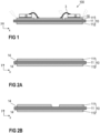
Figure 1 is a cross-sectional view of a power semiconductor module arrangement. -
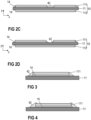
Figure 2 , includingFigures 2A to 2D , schematically illustrates a method for producing a substrate according to one example. -
Figure 3 schematically illustrates a metallization layer on a dielectric insulation layer according to one example. -
Figure 4 schematically illustrates a metallization layer on a dielectric insulation layer according to another example. -
Figure 5 schematically illustrates a metallization layer on a dielectric insulation layer according to an even further example. - In the following detailed description, reference is made to the accompanying drawings. The drawings show specific examples in which the invention may be practiced. It is to be understood that the features and principles described with respect to the various examples may be combined with each other, unless specifically noted otherwise. In the description, as well as in the claims, designations of certain elements as "first element", "second element", "third element" etc. are not to be understood as enumerative. Instead, such designations serve solely to address different "elements". That is, e.g., the existence of a "third element" does not require the existence of a "first element" and a "second element". An electrical line or electrical connection as described herein may be a single electrically conductive element, or include at least two individual electrically conductive elements connected in series and/or parallel. Electrical lines and electrical connections may include metal and/or semiconductor material, and may be permanently electrically conductive (i.e., non-switchable). A semiconductor body as described herein may be made from (doped) semiconductor material and may be a semiconductor chip or be included in a semiconductor chip. A semiconductor body has electrically connecting pads and includes at least one semiconductor element with electrodes.
- Referring to
Figure 1 , a cross-sectional view of apower semiconductor arrangement 100 is illustrated. Thepower semiconductor arrangement 100 includes asubstrate 10. Thesubstrate 10 includes adielectric insulation layer 11, a (structured) first metallization layer (metallic layer) 111 attached to thedielectric insulation layer 11, and a (structured) second metallization layer (metallic layer) 112 attached to thedielectric insulation layer 11. Thedielectric insulation layer 11 is disposed between the first andsecond metallization layers second metallization layer 112, however, is optional and can be omitted. - Each of the first and
second metallization layers substrate 10 can be a ceramic substrate, that is, a substrate in which thedielectric insulation layer 11 is a ceramic, e.g., a thin ceramic layer. The ceramic can consist of or include one of the following materials: aluminum oxide; aluminum nitride; zirconium oxide; silicon nitride; boron nitride; or any other dielectric ceramic. For example, thedielectric insulation layer 11 can consist of or include one of the following materials: Al2O3, AlN, SiC, BeO or Si3N4. For instance, thesubstrate 10 may, e.g., be an Active Metal Brazing (AMB), or a Direct Copper Bonding (DCB) substrate. - The
substrate 10 can be arranged in a housing (not specifically illustrated). One ormore semiconductor bodies 20 can be arranged on thesubstrate 10. Each of thesemiconductor bodies 20 arranged on thesubstrate 10 can include a diode, an IGBT (Insulated-Gate Bipolar Transistor), a MOSFET (Metal-Oxide-Semiconductor Field-Effect Transistor), a JFET (Junction Field-Effect Transistor), a HEMT (High-Electron-Mobility Transistor), or any other suitable controllable semiconductor element. - The one or
more semiconductor bodies 20 can form a semiconductor arrangement on thesubstrate 10. InFigure 1 , only twosemiconductor bodies 20 are exemplarily illustrated. Thesecond metallization layer 112 of thesubstrate 10 inFigure 1 is a continuous layer. Thefirst metallization layer 111 is a structured layer in the example illustrated inFigure 1 . "Structured layer" means that thefirst metallization layer 111 is not a continuous layer, but includes recesses between different sections of the layer. Such recesses are schematically illustrated inFigure 1 . Thesecond metallization layer 112 can also be a structured layer or may be omitted altogether, for example. Thefirst metallization layer 111 in this example includes three different sections.Different semiconductor bodies 20 can be mounted to the same or to different sections of thefirst metallization layer 111. Different sections of the first metallization layer can have no electrical connection or can be electrically connected to one or more other sections using, e.g.,bonding wires 3.Electrical connections 3 can also include bonding ribbons, connection plates, connection clips, or conductor rails, for example, to name just a few examples. The one ormore semiconductor bodies 20 can be electrically and mechanically connected to thesubstrate 10 by an electricallyconductive connection layer 30. Such an electrically conductive connection layer can be a solder layer, for example. - During the use of the power
semiconductor module arrangement 100, high electric field strengths may be present especially at the edges of the different sections of thefirst metallization layer 111 which may cause unwanted breakthroughs. This is schematically illustrated by means of the flashes inFigure 1 . Further, the edges of themetallization layers metallization layers semiconductor module arrangement 100 and significantly reduce its lifetime. - When producing an Active Metal Brazing (AMB) substrate, a metallic layer, e.g., a metal foil, is arranged on a dielectric insulation layer with a connection layer such as, e.g., a solder layer, arranged between the metallic layer and the dielectric insulation layer. When heated, the connection layer melts and the metallic layer is soldered to the dielectric insulation layer.
- A method for producing a Direct Copper Bonding (DCB) substrate generally includes arranging a metallic layer on a dielectric insulation layer, e.g., a ceramic layer. A thin oxide layer is arranged between the metallic layer and the dielectric insulation layer. When the dielectric insulation layer with the metallic layer arranged thereon is heated to above a defined threshold temperature, a metal-oxygen eutectic forms which permanently bonds the metallic layer to the dielectrically insulating layer.
- Now referring to
Figure 2 , a method for producing asubstrate 10 according to one example is schematically illustrated. In a first step, at least onemetallic layer dielectric insulation layer 11, e.g., a ceramic layer. Thedielectric insulation layer 11 can comprise or consist of Al2O3, AlN, SiC, BeO or Si3N4, for example. Other materials are also possible. Each of the at least onemetallic layer Figure 2A , a firstmetallic layer 111 is arranged on one side of thedielectric insulation layer 11, while a secondmetallic layer 112 is arranged on an opposite side of thedielectric insulation layer 11. It is, however, possible to arrange one or moremetallic layers dielectric insulation layer 11. For example, different sections of a metallic layer (see, e.g.,first metallization layer 111 ofFigure 1 ) may be formed on the same side of thedielectric insulation layer 11. It is, however, also possible to arrange a singlemetallic layer 111 on a first side of thedielectric insulation layer 11 and, in an optional step (seeFigure 2B ), form different sections of themetallization layer 111 by structuring the single metallic layer 111 (e.g., by means of an etching process). Aconnection layer 14 is arranged between each of the at least onemetallic layer dielectric insulation layer 11. - The
connection layer 14 can be a solder layer as is used in conventional methods for producing AMB substrates, for example. Theconnection layer 14 may be applied as a paste or solder preform (platelet), for example. Theconnection layer 14 can also be an oxide layer, for example, as is required for the production of DCB substrates. Other kinds of connection layers 14, however, are generally possible which are configured to melt at high temperatures and form a permanent connection between the at least onemetallic layer dielectric insulation layer 11. - Now referring to
Figure 2C , in a subsequent step, a glass powder orglass paste 40 is arranged on thedielectric insulation layer 11. The glass powder orglass paste 40 may be arranged along at least one lateral surface of the at least oneconnection layer 14 and the respective lateral surface of the at least onemetallic layer 111 such that the glass powder orglass paste 40 entirely covers the at least one lateral surface of theconnection layer 14 and at least partly covers the respective lateral surface of themetallic layer 111. A lateral surface is a surface which is essentially perpendicular to a top surface of thedielectric insulation layer 11, wherein the top surface of thedielectric insulation layer 11 is a surface on which the firstmetallic layer 111 is arranged. - In the example illustrated in
Figure 2C , all lateral surfaces of all connection layers arranged on a first side of thedielectric insulation layer 11 are completely covered by the glass powder orglass paste 40, and all lateral surfaces of allmetallic layers 111 arranged on the same side of thedielectric insulation layer 11 are partly covered by the glass powder orglass paste 40. The glass powder orglass paste 40 may comprise or consist of silicate glass or sapphire glass, for example. - Now referring to
Figure 2D , the arrangement is then heated to temperatures of above the melting point of the material of theconnection layer 14 and of the glass powder orglass paste 40. According to one example, the arrangement is heated to temperatures of above 1000°C, which is typically above the melting point of the material of theconnection layer 14 and of the glass powder orglass paste 40. Other temperatures, however, are possible, depending on the specific melting points of the materials. When heated, the at least oneconnection layer 14 melts. At the same time, the glass powder orglass paste 40 melts as well. The glass powder orglass paste 40 may have the same or a similar melting point as the material that is used to form theconnection layer 14. The temperature, however, may be below the melting point of the at least onemetallic layer 111. The at least onemetallic layer 111 may have a melting point that is higher than the melting point of theconnection layer 14 and the glass powder orglass paste 40 such that themetallic layers 111 do not melt during the heating step. When the material of theconnection layer 14 melts during the heating step, the glass powder orglass paste 40 arranged along at least one lateral surface of the at least oneconnection layer 14 prevents the material of theconnection layer 14 from blurring or melting away in an uncontrolled way. Further, the at least onemetallic layer 111 is prevented by the glass powder orglass paste 40 from unintentionally shifting out of place on the meltedconnection layer 14. - When the arrangement is subsequently cooled, the at least one
metallic layer 111 is permanently attached to thedielectric insulation layer 11. The glass powder orglass paste 40 hardens and forms apassivation layer 42 entirely covering the at least one lateral surface of theconnection layer 14 and at least partly covering the respective lateral surface of themetallic layer 111. The edges of themetallic layers passivation layer 42 as has been described above. The edges of themetallic layers 111, therefore, are protected by thepassivation layer 42 during the subsequent use of the power semiconductor module arrangement. During the heating step, some components (e.g., metals such as silver) from theconnection layer 14 may diffuse into the material of thepassivation layer 42 to a certain extent. This may lead to a reduction of the electric fields at the edges of themetallic layers 111 during the use of the power semiconductor module arrangement. - In the example illustrated in
Figure 2 and described above, the glass powder orglass paste 40 and the resultingpassivation layer 42 only partly cover the respective lateral surfaces of themetallic layer 111. As is schematically illustrated inFigure 3 , however, it is also possible that the glass powder orglass paste 40 and the resultingpassivation layer 42 entirely cover the respective lateral surfaces of themetallic layer 111. As is schematically illustrated inFigure 4 , it is even possible that the glass powder orglass paste 40 and the resultingpassivation layer 42 also partly cover a top surface of themetallic layer 111 close to its edges. - As has been mentioned above, the glass powder or
glass paste 40 may prevent the material of theconnection layer 14 from blurring or melting away in an uncontrolled way during the heating step. An unintentional blurring may at least be significantly reduced. However, as is schematically illustrated inFigure 5 , it is still possible that the material of theconnection layer 14 melts away to a certain degree. However, if this happens, any material pouring out from under themetallic layer 111 is completely covered by the resulting passivation layer 42 (see left side ofmetallic layer 111 inFigure 5 ). If this happens, cavities may form in other areas below the metallic layer 111 (see right side ofmetallic layer 111 inFigure 5 ). While such cavities can be problematic in conventional arrangements, in the arrangements disclosed herein such cavities are filled by the glass powder orglass paste 40 during the heating step. That is, the resultingpassivation layer 42 may also partly be arranged in such cavities below themetallic layer 111. In this way, malfunctioning of the arrangement during its use may also be prevented. - As the glass powder or
glass paste 40 may be melted during the same heating step that is performed to attach themetallic layer 111 to the dielectric insulation layer (metallic layer 111 and glass powder orglass paste 40 may be melted simultaneously), the method is very cost effective. Only one additional step of arranging the glass powder orglass paste 40 on thedielectric insulation layer 11 is required.
Claims (14)
- A method comprises:arranging at least one metallic layer (111) on a dielectric insulation layer (11), with a connection layer (14) arranged between each of the at least one metallic layer (111) and the dielectric insulation layer (11);arranging a glass powder or glass paste (40) on the dielectric insulation layer (11) along at least one lateral surface of the connection layer (14) and the at least one metallic layer (111) such that the glass powder or glass paste (40) entirely covers the at least one lateral surface of the connection layer (14) and at least partly covers the respective lateral surface of the metallic layer (111); andheating and subsequently cooling the dielectric insulation layer (11), the at least one metallic layer (111), the at least one connection layer (14) and the glass powder or glass paste (40) such that each connection layer (14) forms a permanent substance-to-substance bond between a respective on of the at least one metallic layer (111) and the dielectric insulation layer (11), and the glass powder or glass paste (40) melts and subsequently hardens, thereby forming a passivation layer (42) entirely covering the at least one lateral surface of the connection layer (14) and at least partly covering the respective lateral surface of the metallic layer (111).
- The method of claim 1, wherein heating the dielectric insulation layer (11), the at least one metallic layer (111), the at least one connection layer (14) and the glass powder or glass paste (40) comprises heating the dielectric insulation layer (11), the at least one metallic layer (111), the at least one connection layer (14) and the glass powder or glass paste (40) to temperatures of above the melting point of the materials of the at least one connection layer (14) and the glass powder or glass paste (40), and below the melting point of the at least one metallic layer (111).
- The method of claim 1 or 2, wherein the glass powder or glass paste (40) is arranged on the dielectric insulation layer (11) such that it entirely covers the respective lateral surfaces of the metallic layer (111).
- The method of claim 3, wherein the glass powder or glass paste (40) is arranged on the dielectric insulation layer (11) such that it further partly covers a top surface of the metallic layer (111).
- The method of any of claims 1 - 4, wherein arranging at least one metallic layer (111) on a dielectric insulation layer (11) comprises arranging a layer comprising or including copper, a copper alloy, aluminum, or an aluminum alloy on the dielectric insulation layer (11).
- The method of any of the preceding claims, wherein arranging at least one metallic layer (111) on a dielectric insulation layer (11) comprises arranging at least one metallic layer (111) on a layer comprising or consisting of Al2O3, AlN, SiC, BeO or Si3N4.
- The method of any of the preceding claims, wherein arranging a glass powder or glass paste (40) on the dielectric insulation layer (11) comprises arranging a silicate glass or sapphire glass powder or paste on the dielectric insulation layer (11).
- A substrate (10) comprising:a dielectric insulation layer (11);at least one metallic layer (111) permanently attached to the dielectric insulation layer (11) by means of a connection layer (14); anda passivation layer (42) along at least one lateral surface of the connection layer (14) and the at least one metallic layer (111), whereinthe passivation layer (42) entirely covers the at least one lateral surface of the connection layer (14) and at least partly covers the respective lateral surface of the metallic layer (111).
- The substrate (10) of claim 8, wherein the dielectric insulation layer comprises or consists of Al2O3, AlN, SiC, BeO or Si3N4.
- The substrate (10) of claim 8 or 9, wherein the at least one metallic layer (111) consist of or includes one of the following materials: copper; a copper alloy; aluminum; and an aluminum alloy.
- The substrate (10) of any of claims 8 - 10, wherein the passivation layer (42) comprises or consists of silicate glass or sapphire glass.
- The substrate (10) of any of claims 8 - 11, wherein the connection layer (14) is a solder layer or an oxide layer.
- The substrate (10) of any of claims 8 - 12, wherein the passivation layer (42) entirely covers the respective lateral surface of the metallic layer (111).
- The substrate (10) of any of claims 8 - 13, wherein the passivation layer (42) further partly covers a top surface of the metallic layer (111).
Priority Applications (1)
| Application Number | Priority Date | Filing Date | Title |
|---|---|---|---|
| EP22152962.1A EP4215508A1 (en) | 2022-01-24 | 2022-01-24 | Substrate and method for producing a substrate |
Applications Claiming Priority (1)
| Application Number | Priority Date | Filing Date | Title |
|---|---|---|---|
| EP22152962.1A EP4215508A1 (en) | 2022-01-24 | 2022-01-24 | Substrate and method for producing a substrate |
Publications (1)
| Publication Number | Publication Date |
|---|---|
| EP4215508A1 true EP4215508A1 (en) | 2023-07-26 |
Family
ID=80780736
Family Applications (1)
| Application Number | Title | Priority Date | Filing Date |
|---|---|---|---|
| EP22152962.1A Pending EP4215508A1 (en) | 2022-01-24 | 2022-01-24 | Substrate and method for producing a substrate |
Country Status (1)
| Country | Link |
|---|---|
| EP (1) | EP4215508A1 (en) |
Cited By (1)
| Publication number | Priority date | Publication date | Assignee | Title |
|---|---|---|---|---|
| EP4614551A1 (en) * | 2024-03-08 | 2025-09-10 | Infineon Technologies AG | Substrate and method for producing a substrate |
Citations (3)
| Publication number | Priority date | Publication date | Assignee | Title |
|---|---|---|---|---|
| US4163656A (en) * | 1972-06-21 | 1979-08-07 | U.S. Philips Corporation | Method of manufacturing a lead-through of a metal element through a ceramic component by means of sealing |
| US20180093927A1 (en) * | 2016-09-30 | 2018-04-05 | Infineon Technologies Ag | Method for Producing a Metal-Ceramic Substrate, and a Metal-Ceramic Substrate |
| EP3457434A1 (en) * | 2017-09-13 | 2019-03-20 | Infineon Technologies AG | Semiconductor substrate for a power semiconductor module arrangement and method for producing the same |
-
2022
- 2022-01-24 EP EP22152962.1A patent/EP4215508A1/en active Pending
Patent Citations (3)
| Publication number | Priority date | Publication date | Assignee | Title |
|---|---|---|---|---|
| US4163656A (en) * | 1972-06-21 | 1979-08-07 | U.S. Philips Corporation | Method of manufacturing a lead-through of a metal element through a ceramic component by means of sealing |
| US20180093927A1 (en) * | 2016-09-30 | 2018-04-05 | Infineon Technologies Ag | Method for Producing a Metal-Ceramic Substrate, and a Metal-Ceramic Substrate |
| EP3457434A1 (en) * | 2017-09-13 | 2019-03-20 | Infineon Technologies AG | Semiconductor substrate for a power semiconductor module arrangement and method for producing the same |
Cited By (1)
| Publication number | Priority date | Publication date | Assignee | Title |
|---|---|---|---|---|
| EP4614551A1 (en) * | 2024-03-08 | 2025-09-10 | Infineon Technologies AG | Substrate and method for producing a substrate |
Similar Documents
| Publication | Publication Date | Title |
|---|---|---|
| US10283432B2 (en) | Molded package with chip carrier comprising brazed electrically conductive layers | |
| CN103035601B (en) | Include the semiconductor devices of Diffusion Welding layer on sintering silver layer | |
| US6731002B2 (en) | High frequency power device with a plastic molded package and direct bonded substrate | |
| US10510640B2 (en) | Semiconductor device and method for manufacturing semiconductor device | |
| CN102593081B (en) | Comprise the semiconductor device of radiator | |
| KR100957078B1 (en) | Electrically Isolated Power Device Package | |
| US7682875B2 (en) | Method for fabricating a module including a sintered joint | |
| EP3276657A1 (en) | Cooler, power semiconductor module arrangement having a cooler, and methods for producing the same | |
| CN104064529B (en) | The method of semiconductor devices, semiconductor module and manufacture semiconductor devices and semiconductor module | |
| US12564094B2 (en) | Power semiconductor module arrangement and method for producing the same | |
| EP3739756A1 (en) | Cascode semiconductor device and method of manufacture | |
| JP5954374B2 (en) | Insulating substrate, manufacturing method thereof, semiconductor module, and semiconductor device | |
| EP4084062A1 (en) | Power semiconductor module arrangement | |
| KR100957079B1 (en) | Power device with plastic casting package and direct bonded substrate | |
| EP3696851A1 (en) | Semiconductor arrangement and method for producing the same | |
| EP3627546A1 (en) | Power semiconductor module arrangement | |
| EP4346341A1 (en) | Method for forming a power semiconductor module arrangement | |
| EP4428914A1 (en) | Power semiconductor module arrangement | |
| EP4601000A1 (en) | Power semiconductor module arrangement and method for producing the same | |
| US20250218887A1 (en) | Semiconductor device and manufacturing method of semiconductor device | |
| EP4439649A1 (en) | Substrate arrangement | |
| EP4576199A1 (en) | Substrate and methods for producing a substrate | |
| EP4607582A1 (en) | Semiconductor module arrangement | |
| EP3951866A1 (en) | Semiconductor substrate arrangement and method for producing the same | |
| EP3457434A1 (en) | Semiconductor substrate for a power semiconductor module arrangement and method for producing the same |
Legal Events
| Date | Code | Title | Description |
|---|---|---|---|
| PUAI | Public reference made under article 153(3) epc to a published international application that has entered the european phase |
Free format text: ORIGINAL CODE: 0009012 |
|
| STAA | Information on the status of an ep patent application or granted ep patent |
Free format text: STATUS: REQUEST FOR EXAMINATION WAS MADE |
|
| 17P | Request for examination filed |
Effective date: 20221212 |
|
| AK | Designated contracting states |
Kind code of ref document: A1 Designated state(s): AL AT BE BG CH CY CZ DE DK EE ES FI FR GB GR HR HU IE IS IT LI LT LU LV MC MK MT NL NO PL PT RO RS SE SI SK SM TR |
|
| STAA | Information on the status of an ep patent application or granted ep patent |
Free format text: STATUS: EXAMINATION IS IN PROGRESS |
|
| 17Q | First examination report despatched |
Effective date: 20251008 |