EP4213392A1 - Elimination of probability of bit errors in successive approximation register (sar) analog-to-digital converter (adc) logic - Google Patents
Elimination of probability of bit errors in successive approximation register (sar) analog-to-digital converter (adc) logic Download PDFInfo
- Publication number
- EP4213392A1 EP4213392A1 EP22209314.8A EP22209314A EP4213392A1 EP 4213392 A1 EP4213392 A1 EP 4213392A1 EP 22209314 A EP22209314 A EP 22209314A EP 4213392 A1 EP4213392 A1 EP 4213392A1
- Authority
- EP
- European Patent Office
- Prior art keywords
- output
- comparator
- circuitry
- logic circuitry
- digital
- Prior art date
- Legal status (The legal status is an assumption and is not a legal conclusion. Google has not performed a legal analysis and makes no representation as to the accuracy of the status listed.)
- Pending
Links
Images



Classifications
-
- H—ELECTRICITY
- H03—ELECTRONIC CIRCUITRY
- H03M—CODING; DECODING; CODE CONVERSION IN GENERAL
- H03M1/00—Analogue/digital conversion; Digital/analogue conversion
- H03M1/10—Calibration or testing
- H03M1/1009—Calibration
-
- H—ELECTRICITY
- H03—ELECTRONIC CIRCUITRY
- H03M—CODING; DECODING; CODE CONVERSION IN GENERAL
- H03M1/00—Analogue/digital conversion; Digital/analogue conversion
- H03M1/06—Continuously compensating for, or preventing, undesired influence of physical parameters
- H03M1/0617—Continuously compensating for, or preventing, undesired influence of physical parameters characterised by the use of methods or means not specific to a particular type of detrimental influence
- H03M1/0624—Continuously compensating for, or preventing, undesired influence of physical parameters characterised by the use of methods or means not specific to a particular type of detrimental influence by synchronisation
-
- H—ELECTRICITY
- H03—ELECTRONIC CIRCUITRY
- H03M—CODING; DECODING; CODE CONVERSION IN GENERAL
- H03M1/00—Analogue/digital conversion; Digital/analogue conversion
- H03M1/06—Continuously compensating for, or preventing, undesired influence of physical parameters
- H03M1/08—Continuously compensating for, or preventing, undesired influence of physical parameters of noise
- H03M1/0836—Continuously compensating for, or preventing, undesired influence of physical parameters of noise of phase error, e.g. jitter
-
- H—ELECTRICITY
- H03—ELECTRONIC CIRCUITRY
- H03M—CODING; DECODING; CODE CONVERSION IN GENERAL
- H03M1/00—Analogue/digital conversion; Digital/analogue conversion
- H03M1/06—Continuously compensating for, or preventing, undesired influence of physical parameters
- H03M1/08—Continuously compensating for, or preventing, undesired influence of physical parameters of noise
- H03M1/0863—Continuously compensating for, or preventing, undesired influence of physical parameters of noise of switching transients, e.g. glitches
- H03M1/0872—Continuously compensating for, or preventing, undesired influence of physical parameters of noise of switching transients, e.g. glitches by disabling changes in the output during the transitions, e.g. by holding or latching
-
- H—ELECTRICITY
- H03—ELECTRONIC CIRCUITRY
- H03M—CODING; DECODING; CODE CONVERSION IN GENERAL
- H03M1/00—Analogue/digital conversion; Digital/analogue conversion
- H03M1/10—Calibration or testing
- H03M1/1071—Measuring or testing
-
- H—ELECTRICITY
- H03—ELECTRONIC CIRCUITRY
- H03M—CODING; DECODING; CODE CONVERSION IN GENERAL
- H03M1/00—Analogue/digital conversion; Digital/analogue conversion
- H03M1/12—Analogue/digital converters
- H03M1/124—Sampling or signal conditioning arrangements specially adapted for A/D converters
- H03M1/1245—Details of sampling arrangements or methods
- H03M1/125—Asynchronous, i.e. free-running operation within each conversion cycle
-
- H—ELECTRICITY
- H03—ELECTRONIC CIRCUITRY
- H03M—CODING; DECODING; CODE CONVERSION IN GENERAL
- H03M1/00—Analogue/digital conversion; Digital/analogue conversion
- H03M1/12—Analogue/digital converters
- H03M1/34—Analogue value compared with reference values
- H03M1/38—Analogue value compared with reference values sequentially only, e.g. successive approximation type
- H03M1/46—Analogue value compared with reference values sequentially only, e.g. successive approximation type with digital/analogue converter for supplying reference values to converter
- H03M1/462—Details of the control circuitry, e.g. of the successive approximation register
-
- H—ELECTRICITY
- H03—ELECTRONIC CIRCUITRY
- H03M—CODING; DECODING; CODE CONVERSION IN GENERAL
- H03M1/00—Analogue/digital conversion; Digital/analogue conversion
- H03M1/12—Analogue/digital converters
- H03M1/34—Analogue value compared with reference values
- H03M1/38—Analogue value compared with reference values sequentially only, e.g. successive approximation type
- H03M1/46—Analogue value compared with reference values sequentially only, e.g. successive approximation type with digital/analogue converter for supplying reference values to converter
- H03M1/466—Analogue value compared with reference values sequentially only, e.g. successive approximation type with digital/analogue converter for supplying reference values to converter using switched capacitors
-
- H—ELECTRICITY
- H03—ELECTRONIC CIRCUITRY
- H03M—CODING; DECODING; CODE CONVERSION IN GENERAL
- H03M1/00—Analogue/digital conversion; Digital/analogue conversion
- H03M1/12—Analogue/digital converters
- H03M1/34—Analogue value compared with reference values
- H03M1/38—Analogue value compared with reference values sequentially only, e.g. successive approximation type
- H03M1/46—Analogue value compared with reference values sequentially only, e.g. successive approximation type with digital/analogue converter for supplying reference values to converter
- H03M1/466—Analogue value compared with reference values sequentially only, e.g. successive approximation type with digital/analogue converter for supplying reference values to converter using switched capacitors
- H03M1/468—Analogue value compared with reference values sequentially only, e.g. successive approximation type with digital/analogue converter for supplying reference values to converter using switched capacitors in which the input S/H circuit is merged with the feedback DAC array
Definitions
- the present disclosure generally relates to electronics, and, more specifically, to successive approximation register (SAR) analog-to-digital converters (ADCs).
- SAR successive approximation register
- ADCs analog-to-digital converters
- an analog input signal is converted to a digital output signal (e.g., for further digital signal processing).
- a digital output signal e.g., for further digital signal processing.
- electronics are provided with one or more sensors to make measurements, and these sensors can generate an analog signal.
- the analog signal can then be provided to an analog-to-digital converter (ADC) circuit as input to generate a digital output signal for further processing.
- ADC analog-to-digital converter
- an antenna in a wireless communication device receiver or a base station receiver, an antenna can generate an analog signal based on the electromagnetic waves carrying information/signals in the air.
- the analog signal generated by the antenna can then be provided as input to an ADC to generate a digital output signal for further processing.
- a SAR ADC may implement a binary search algorithm to convert an analog input voltage into a digital code (e.g., an N-bit value). To perform the binary search, the SAR ADC may perform successive comparisons of an analog input voltage to a series of analog test voltages (e.g., digitally-controlled test voltages) and using the result from each comparison to generate a digital code to represent a magnitude of the analog input voltage.
- a series of analog test voltages e.g., digitally-controlled test voltages
- the SAR ADC may include sample-and-hold (S/H) circuitry to acquire a sample of the analog input voltage and hold the sampled analog input voltage to a constant value for the successive comparisons, a digital-to-analog-converter (DAC) to generate the analog test voltages, a comparator to compare the sampled analog input voltage to each of the analog test voltages, and SAR logic circuitry (e.g., digital circuitry) to control the generation of the digital code based on each of the comparison results.
- S/H sample-and-hold
- DAC digital-to-analog-converter
- comparator to compare the sampled analog input voltage to each of the analog test voltages
- SAR logic circuitry e.g., digital circuitry
- the SAR logic circuitry may take the output of the comparator, record a bit value (for the N-bit value) according to the output of the comparator, and using the recorded value to update the DAC for a next iteration of the binary search (or bit trial).
- the comparator may generate two outputs, one for a positive result and another one for a negative result while the SAR logic circuitry may generate the same number of outputs as the conversion resolution (e.g., N bits).
- the SAR logic circuitry may utilize a shift register to window the comparator's outputs to the correct SAR logic circuitry output (e.g., setting a value for a bit within the N-bit value).
- a forbidden (or illegal) state may exist in the SAR logic circuitry in which the same SAR logic output (a bit within the N-bit value) cannot be written to twice as it would cause not only the bit being overwritten to be erroneous but all subsequent bits to be erroneous.
- a bit error in the SAR logic circuitry due to the forbidden state may also be referred to as a probabilistic error.
- the forbidden state may be triggered when the SAR ADC is pushed to operate at a high speed (e.g., with a sampling rate of hundreds of megahertz (MHz)). For instance, when the SAR ADC is clocked at a high speed, the edges of the clock signals and/or the windowing signal (e.g., shift register output) in the SAR logic circuitry can become rounded (e.g., a slow-roll off transition from a logic high to a logic low, or vice versa).
- the edge rate of the shift register output can be improved using additional circuitry. However, this may only reduce the probability of the forbidden state from occurring and does not eliminate the occurrences of the forbidden state.
- the additional circuitry can increase cost, power, and/or area for the SAR ADC.
- the SAR logic circuitry may utilize flops in the main signal path of the SAR logic circuitry to better gate various circuit decisions.
- flops may have a large propagation delay, and thus may limit the speed at which the SAR logic circuitry can operate. Accordingly, technique improvements for SAR logic circuitry can be beneficial.
- the present disclosure describes mechanisms for providing a high-speed SAR ADC in a manner that can eliminate the probability of SAR logic circuitry from writing a logical value to the same conversion result twice, for example, by logically gating the SAR ADC's comparator outputs using opposite polarity information. That is, the positive output of the comparator may be gated by a digital result associated with a negative output of the comparator, and the negative output of the comparator may be gated by a digital result associated with a positive output of the comparator in a feedback manner.
- One aspect of the present disclosure provides a SAR ADC including a DAC, a comparator, and SAR logic circuitry.
- the DAC may generate a first DAC output voltage based on a digital output code (e.g., a test value) associated with an analog input voltage (e.g., a sample analog input voltage).
- the comparator may compare the first DAC output voltage to the analog input voltage to generate a comparison result including a positive output and a negative output.
- the SAR logic circuitry may include first logic circuitry and second logic circuitry downstream of the first logic circuitry.
- the first logic circuitry may gate at least one of the first positive output or the first negative output of the comparator to the second logic circuitry based at least in part on a digital feedback.
- the digital feedback may include information associated with at least one of an opposite polarity of the first positive output or the first negative output.
- the second logic circuitry may include latching circuitry and/or reset circuitry, and the digital feedback may correspond to an output downstream of the reset circuitry.
- the first positive output and the first negative output from the comparator may be associated with a current bit trail, and the digital feedback may be associated with a previous bit trial.
- the digital feedback may include an output of the second logic circuitry, where the output is responsive to at least one of a second positive output or a second negative output of the comparator.
- the DAC may generate a second DAC output voltage based on a previous digital output code (e.g., a previous test value) associated with the analog input voltage, and the comparator may compare the second DAC output voltage to the analog input voltage to generate a comparison result including the second positive output and the second negative output.
- the first logic circuitry may gate the first positive output of the comparator to the second logic circuitry based on the first positive output having a logic one value and the digital feedback indicating the output responsive to the second negative output of the comparator also has a logic one value. In some aspects, as part of the gating, the first logic circuitry may gate the first negative output of the comparator to the second logic circuitry based on the first negative output having a logic one value and the digital feedback indicating the output responsive to the second positive output of the comparator also has a logic one value.
- the SAR logic circuitry may include a shift register that generates output clock pulses, for example, to track the bit position within the digital output code for each bit trial.
- the occurrences of the forbidden state may be caused by a shift register output clock pulse for a previous bit trial partially overlaps with a shift register output clock pulse for a current bit trial and remains active when the comparator outputs a comparison result for the current bit trial.
- the gating of the comparator output (e.g., the positive output and the negative output) to the second logic circuitry may be based on a detection of a shift register output clock pulse associated with the previous bit trial remaining active after the comparator generated the first positive output and the first negative output for the current bit trial.
- the first logic circuitry may include a NOT-AND (NAND) gate with three inputs.
- the NAND gate may include a first input to receive the first positive output of the comparator, a second input to receive the digital feedback, and a third input to receive a shift register output clock pulse.
- the SAR logic circuitry may further include asynchronous clock generation circuitry to generate a first comparator clock pulse for the previous bit trial and generate a second comparator clock pulse for the current bit trial, where the second comparator clock pulse may be generated in response to a completion of the previous bit trial.
- the systems, schemes, and mechanisms described herein advantageously enable a SAR ADC to operate at a high speed (e.g., about 100 MHz, 160 MHz, 200 MHz, 220 MHz or more) without the probability of entering a forbidden state. Further, adding the digital feedback circuitry may not increase the SAR logic circuitry complexity, power, area, and/or cost significantly. Accordingly, the disclosed embodiments can provide an efficient and effective solution to eliminate the forbidden state from the SAR logic circuitry.
- the disclosed SAR ADC may be suitable for use in a wide variety of applications such as audio, wireless communications, instrumentations, energy, health and diagnostic, etc.
- FIG. 1 is a block diagram illustrating an SAR ADC 100.
- the SAR ADC 100 may be used for a broad range of applications, such as audio, communications, energy, healthcare, instrumentation and measurement, motor and power control, industrial automation, and/or aerospace/defense, to convert analog signals to digital values, which can be used for further digital processing.
- the SAR ADC 100 may include a switched capacitor DAC 110, a comparator 120, and SAR logic circuitry 130.
- the switched capacitor DAC 110 may include S/H circuitry 112, a signal summer 114, and a DAC 116.
- the SAR ADC 100 may receive an analog input voltage 102 shown as Vin and generate a digital representation (e.g., a digital output code 104 shown as Dout) of the analog input voltage 102 using a binary search algorithm.
- the SAR ADC 100 may be single-ended or differential. That is, the analog input voltage 102 can be a single-ended voltage (with respect to a ground potential) or a differential voltage. Accordingly, the components of the SAR ADC 100 can be single-ended or differential.
- the operations of the SAR ADC 100 may include a sampling phase followed by a conversion phase.
- the S/H circuitry 112 may acquire or capture a sample of the analog input voltage 102 and hold the sampled voltage 113 (e.g., a constant value) during the following conversion phase.
- the SAR ADC 100 may perform conversion one bit at a time by performing a binary search.
- the SAR ADC 100 may perform N number of bit trials to generate an N-bit digital output code 104 (e.g., represented by ⁇ b N-1 , ..., bo>).
- the SAR logic circuitry 130 may begin with setting an N-bit value (e.g., stored in a register) to a midscale.
- the DAC 116 may receive the N-bit value and output a first test voltage 117 (e.g., of a series of test voltages 117) according to the N-bit value.
- the DAC 116 may be provided with a reference voltage V REF , and the first test voltage 117 may correspond to V REF /2 based on the N-bit value having the MSB set to 1 and all other bits set to 0.
- the comparator 120 may compare the sampled voltage 113 to the first test voltage 117 to determine whether the sampled voltage is greater than, or less than the first test voltage 117, for example, by subtracting the first test voltage 117 from the sampled input voltage 113 using the signal summer 114 as shown.
- the comparator 120 may have a positive or non-inverting input terminal and a negative or inverting terminal, where the positive input terminal may be coupled to the output of the S/H circuitry 112 and the negative input terminal may be coupled to the output of the DAC 116. That is, the signal summer 114 may be implemented as part of the comparator 120.
- the comparator 120 may output a logic high (e.g., a comparison result 122), and the SAR logic circuitry 130 may maintain the logic 1 for the MSB of the N-bit. If, however, the sampled voltage 113 is less than the first test voltage 117, the comparator 120 may output a logic low (e.g., a comparison result 122), and the SAR logic circuitry 130 may clear the MBS of the N-bit value to a logic 0.
- the SAR logic circuitry 130 may move on to perform a next bit trial to determine a bit value for the next bit (e.g., b N-2 ) in the N-bit value in a similar way as for the MSB. For instance, the SAR logic circuitry 130 may set the next bit in the N-bit value to a 1, the DAC 116 may generate a second test voltage 117 (e.g., of a series of test voltages 117) based on the updated N-bit value, the comparator 120 may compare the sampled voltage 113 to the second test voltage 117, and the SAR logic circuitry 130 may update the N-bit value according to the comparison result 122 for the second test voltage 117.
- the SAR logic circuitry 130 may set the next bit in the N-bit value to a 1
- the DAC 116 may generate a second test voltage 117 (e.g., of a series of test voltages 117) based on the updated N-bit value
- the comparator 120 may compare the sampled voltage 113 to the
- the bit trial process may continue for each subsequent bit of the N-bit value down to the LSB (e.g., b 0 ). Once the last bit trial for the LSB is completed, the SAR logic circuitry 130 may output the N-bit value as the digital output code 104.
- the DAC 116 may include an array of switched capacitors (e.g., binary-weighted capacitors) connected in parallel, where a first end of each of the capacitors may be selectively coupled to the analog input terminal (where Vin is received), V REF , or GND, and a second, opposite end of each of the capacitors may be coupled to a common terminal.
- the first end may be coupled to three switches, each coupled to a different one of the analog input terminal, V REF , or a ground potential (e.g., GND).
- the analog input voltage 102 may be applied to charge the capacitors, for example, the first end of each of the capacitors may be selectively coupled to the analog input terminal of the SAR ADC 100 to receive the analog input voltage 102 and the second end of each of the capacitors may be selectively coupled to the common terminal.
- the capacitors may be charged to a voltage substantially equal to the analog input voltage 102.
- connections of the capacitors are switched, for example, the first end of each of the capacitors may be selectively coupled to V REF or GND, and the second end may remain coupled to the common terminal.
- the connections or switches may be controlled using a digital code (e.g., the N-bit value stored in the register) from the SAR logic circuitry 130.
- the DAC 116 may generate a test voltage 117 at the common terminal.
- the test voltage 117 at the common terminal may be input to the comparator 120 for comparison against the sampled voltage 113.
- the SAR logic circuitry 130 may set the respective bit of the N-bit value based on the output of the comparator 120, and control the switches or connections of the capacitors by selectively coupling the first end of the capacitor to V ref or GND according to the respective bit value.
- the SAR ADC 100 may receive an external ADC clock signal 101 that drives the operations of the S/H circuitry 112.
- the external ADC clock signal 101 may be configured in a variety of ways. In some examples, the external ADC clock signal 101 may control the sampling period and the conversion period of the SAR ADC 100 and the rate at which the SAR ADC 100 samples the analog input voltage signal 102.
- the external ADC clock signal 101 may also be provided to the SAR logic circuitry 130.
- the SAR logic circuitry 130 may begin an initial bit trial (e.g., the bit trial for MSB, b N-1 ) based on the ADC clock signal 101, but may generate an asynchronous clock signal 132 (shown as CLKC) internally to latch the output signal of the comparator 120.
- the asynchronous clock signal 132 may be referred to as a comparator output clock signal. The generation and operations of the comparator output clock signal 132 and the operations of the SAR logic circuitry 130 are discussed more fully below with reference to FIG. 2 .
- FIG. 2 is a schematic block diagram illustrating an exemplary SAR ADC portion 200, according to some embodiments of the present disclosure.
- the SAR ADC portion 200 may correspond to a portion of the SAR ADC 100 of FIG. 1 and may provide a more detailed view of the SAR logic circuitry 130.
- the SAR logic circuitry 130 may include a shift register 210, asynchronous clock generation circuitry 260, NAND gates 220 and 222 (each with two inputs), latching circuitries 230 and 240, and buffer gates 250 and 252.
- NAND gates 220 and 222 each with two inputs
- latching circuitries 230 and 240 latching circuitries 230 and 240
- buffer gates 250 and 252 buffer gates
- the SAR logic circuitry 130 is illustrated with circuitries (e.g., the NAND gates 220 and 222, the latching circuitries 230 and 240, and the buffer gates 250 and 252) for generating one bit.
- the SAR logic circuitry 130 can include similar circuitries (e.g., the NAND gates 220 and 222, the latching circuitries 230 and 240, and the buffer gates 250 and 252) for each bit. That is, to provide an ADC resolution of N bits, the SAR logic circuitry 130 may include N number of the circuitry including the NAND gates 220 and 222, the latching circuitries 230 and 240, and the buffer gates 250 and 252 arranged as shown. Further, the SAR logic circuitry 130 can include any suitable number of latching stages, buffering stages, and/or inverting stages, connected to each of the comparator outputs 202 and 204.
- the SAR logic circuitry 130 may perform N number of bit trials, one for each bit.
- the SAR logic circuitry 130 may track the bit position within the N-bit value for each bit trial using the shift register 210.
- the shift register 210 may correlate or associate a certain comparison to a corresponding bit position within the N-bit value.
- the shift register 210 may output a series of clock pulses 212, one for each bit trial.
- the clock signal pulses 212 may be shown as CLKS ⁇ N-1:0>, where CLKS ⁇ N-1> may represent the clock pulse for the MSB bit trial and CLKS ⁇ 0> may represent the clock pulse for the LSB bit trial.
- the shift register 210 may be implemented using any suitable gates and logic circuitry and may be clocked or driven by the comparator output clock signal 132. For instance, the shift register 210 may output the clock pulse 212 sequentially from CLKS ⁇ N-1> to CLKS ⁇ 0>, each triggered by an assertion (e.g., a rising edge) of the comparator output clock signal 132. In some examples, the shift register 210 may be implemented using a sequence of flops connected in series and clocked by the comparator output clock signal 132. For instance, the shift register 210 may include N number of flops connected in series, and each flop may be sequentially triggered to generate a shift register output clock pulse 212 by a corresponding clock pulse of the comparator output clock signal 132.
- the comparator 120 may compare a DAC output voltage V DAC (e.g., a test voltage 117 output by the DAC 116) to a sampled analog input voltage (e.g., the analog input voltage 102) and generate a comparison result. More specifically, the comparator 120 may output a positive output 202 represented by C op (e.g., at a positive output terminal shown by the "+” symbol) and a negative output 204 represented by C on (e.g., at a negative output terminal shown by the "-” symbol). Each of the positive output 202 and the negative output 204 may be a logic high or a logic low.
- a logic high for the positive output 202 may indicate a bit value of 1 for the respective bit
- a logic high for the negative output 204 may indicate a bit value of 0 for the respective bit. Because a bit value can only be 1 or 0, one of the positive output 202 or the negative output 204 may have a logic high, and the other one of the positive output 202 or the negative output 204 may have a logic low under normal operations. That is, the positive output 202 and the negative output 204 may be complementary of each other when the comparator 120 converges to a decision.
- the comparator 120 may latch the comparison result to the output terminals according to the comparator output clock signal 132.
- the comparator 120 may perform a comparison upon detecting an assertion (e.g., a rising edge) of a clock pulse in the comparator output clock signal 132, for example, by responding to a difference between the sampled voltage and the DAC output voltage V DAC , and may output the comparison result.
- the positive output 202 of the comparator 120 and a respective shift register output clock pulse 212 may be coupled to the inputs of the NAND gate 220.
- the NAND gate 220 may operate as a latch, gating the positive output 202 to the latching circuitry 230 based on the respective shift register output clock pulse 212.
- the NAND gate 220 may generating an output 221 represented by set p ⁇ k> for the k th bit (e.g., within set p ⁇ N-1:0>) when the respective shift register output clock pulse 212 is asserted (a logic high).
- the negative output 204 of the comparator 120 and the respective shift register output clock pulse 212 may be coupled to the inputs of the NAND gate 222.
- the NAND gate 222 may gate the negative output 204 to the latching circuitry 240 based on the respective shift register output clock pulse 212, for example, by generating an output 223 represented by set n ⁇ k> for the k th bit (e.g., within set n ⁇ N-1:0>) when the respective shift register output clock pulse 212 is asserted.
- the NAND gates 220 and 222 may output set p ⁇ k> and set n ⁇ k>, respectively, for the k th bit upon a completion of the comparison (by the comparator 120) for the k th bit and an assertion of the respective shift register output clock pulse 212. Accordingly, the shift register output clock pulse 212 may operate to window the outputs 202 and 204 of the comparator 120 for a particular bit trial.
- the latching circuitry 230 may be coupled to the output of the NAND gate 220.
- the latching circuitry 230 may receive the output 221 set p ⁇ k> from the NAND gate 220 and lock or retain the bit value of set p ⁇ k> until a reset is applied to the latching circuitry 230.
- the latching circuitry 240 may be coupled to the output of the NAND gate 222.
- the latching circuitry 240 may receive the output 223 set n ⁇ k> from the NAND gate 222 and lock or retain the bit value of set n ⁇ k> until a reset is applied to the latching circuitry 240.
- the latching circuitry 230 is implemented using a set-reset (SR) flip-flop or including a pair of cross-coupled 2-input NAND gates 232 and 234.
- the latching circuitry 240 is implemented as an SR flip-flop including a pair of cross-coupled 2-input NAND gates 242 and 244.
- the buffer gate 250 may be coupled to the output of the latching circuitry 230.
- the buffer gate 250 may receive the latched output 235 (corresponding to set p ⁇ k>) and pass the output 235 (e.g., with a delay) to the output 251 represented by dpb ⁇ k> for the k th bit (e.g., within dpb ⁇ N-1,0>).
- the buffer gate 252 may be coupled to the output of the latching circuitry 240.
- the buffer gate 252 may receive the latched output 245 (corresponding to set n ⁇ k>) and pass the output 245 (e.g., with a delay) to the output 253 represented by dnb ⁇ k> for the k th bit (e.g., within dnb ⁇ N-1,0>).
- set p ⁇ k> may be a logic low when the positive output 202 C op ⁇ k> is a logic high and CLKS ⁇ k> is asserted (a logic high). Conversely, set p ⁇ k> may be a logic high when the positive output 202 C op ⁇ k> is a logic low and CLKS ⁇ k> is asserted. Similarly, based on the NAND gate 222 operations, set n ⁇ k> may be a logic low when the negative output 204 C on ⁇ k> is a logic high and CLKS ⁇ k> is asserted.
- set n ⁇ k> may be a logic high when the negative output 204 C on ⁇ k> is a logic low and CLKS ⁇ k> is asserted.
- the SR flip-flop with the NAND gates 232 and 234 may retain its value when set p ⁇ k> is low until a reset (e.g., assertion of Q rstb ) is applied to the SR flip-flop (meaning that the SR flip-flop is active low).
- the SR flip-flop with the NAND gates 242 and 244 may retain its value when set p ⁇ k> is low until a reset (e.g., assertion of Q rstb ) is applied to the SR flip-flop.
- dpb ⁇ k> may be a logic high when set p ⁇ k> is a logic low
- dnb ⁇ k> may be a logic high when set n ⁇ k> is a logic low.
- dpb ⁇ k> may be a logic high when C op ⁇ k> is a logic high
- dnb ⁇ k> may be a logic high when C on ⁇ k> is a logic high.
- the SAR logic circuitry 130 may update the k th bit in the N-bit value (e.g., the test value) and configure the capacitors in the DAC 116, for example, by selectively switching a capacitor corresponding to the k th bit to VREF or GND, according to the output 251 and/or 253.
- the SAR logic circuitry 130 may update the k th bit in the N-bit value (e.g., the test value) and configure the capacitors in the DAC 116 by selectively switching a capacitor corresponding to the k th bit to +VREF or - VREF (e.g., depending on the DAC design) according to the output 251 and/or 253.
- the comparator output clock signal 132 can be generated internally at the SAR logic circuitry 130.
- the asynchronous clock generation circuitry 260 may be coupled to the output terminals of the comparator 120.
- the asynchronous clock generation circuitry 260 may receive the outputs 202 and 204 and may generate the comparator output clock signal 132 based at least in part on the outputs 202 and 204.
- the comparator 120 may be reset, for example, the positive output 202 and the negative output 204 may each be cleared to a logic low.
- each of the latching circuitry 230 and the latching circuitry 240 may be reset, for example, by asserting Q rstb at each of the respective SR flip-flops. After the reset, the asynchronous clock generation circuitry 260 may assert a clock pulse for the comparator output clock signal 132 to begin a new comparison or bit trial.
- the assertion of the comparator output clock pulse may trigger a new comparison output at the comparator 120.
- the asynchronous clock generation circuitry 260 may monitor the positive output 202 and the negative output 204 of the comparator 120 to determine when the comparator 120 has completed the comparison and converge to a decision. Because both the positive output 202 and the negative output 204 were cleared to a logic low at reset, the asynchronous clock generation circuitry 260 can detect that the comparator 120 has converged to a decision when the positive output 202 transition to a logic high or when the negative output 204 transition to a logic high.
- the asynchronous clock generation circuitry 260 may de-assert the comparator output clock pulse. After the comparator output clock pulse is de-asserted, the SAR logic circuitry 130 may reset the comparator 120 outputs 202 and 204 and the latching circuitries 230 and 240 as discussed above.
- the asynchronous clock generation circuitry 260 may assert another clock pulse for the comparator output clock signal 132 to trigger a next bit trial.
- the SAR logic circuitry 130 may further include clock edge detection and delay circuitries to control the duration of the reset period and the assertion of the reset signals Q rstb .
- the timing relationships among the signals (e.g., the comparator output clock signal 132, the shift register output 212, and the outputs 202 and 204 of the comparator 120) in the SAR logic circuitry 130 are discussed more fully below with reference to FIG. 3 .
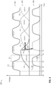
- FIG. 3 is a timing diagram 300 illustrating a probabilistic error in a SAR ADC (e.g., at the SAR logic circuitry 130), according to some embodiments of the present disclosure.
- the x-axes may represent timing in some constant units
- the y-axes may represent voltages in some constant units.
- the graph 302 illustrates an exemplary curve 310 corresponding to a comparator output clock signal 132 of FIG. 1 and/or FIG. 2 .
- the comparator output clock signal 132 may include a series of clock pulses shown as CLKC ⁇ 10> to CLKC ⁇ 7>, for example, for testing bit 10 to bit 7, respectively, within the N-bit value (e.g., a test value) discussed above with reference to FIGS. 1 and 2 .
- N is 11, and thus bit 10 is the MSB.
- the graph 304 illustrates exemplary curves 320, 322, 324, and 326 corresponding to the shift register output clock pulses 212.
- the curves 320 (shown by the solid line), 322 (shown by the dashed line), 324 (shown by the dotted line), and 326 (shown by the dashed-dotted line) may correspond to CLKS ⁇ 10>, CLKS ⁇ 9>, CLKS ⁇ 8>, and CLKS ⁇ 7>, respectively.
- the graph 306 illustrates exemplary curves 330 (shown by the solid line) and 332 (shown by the dashed line) corresponding to the comparator 120's positive output 202 C op and negative output 204 C on , respectively.
- both C op and C on are logic low, for example, after the SAR logic circuitry 130 is reset where bit 10 of the test value is set to 1 and all other bits of the test value are set to 0, and the switches for the capacitors in the DAC 116 are configured according to the test value.
- the asynchronous clock generation circuitry 260 may assert CLKC ⁇ 10>.
- the comparator 120 may compare a sampled input voltage 113 to a first DAC output voltage (e.g., generated by the DAC 116 with bit 10 set to 1 and all other bits set to 0). After a certain delay, at time T2, the comparator 120 may output a comparison result for bit 10.
- C op transitions to a logic high and C on remains a logic low indicating that the sampled input voltage 113 is greater than the first DAC output voltage.
- the shift register 210 is also clocked by the comparator output clock signal 132.
- the shift register output clock pulse CLKS ⁇ 10> for bit 10 may transition to a logic high (e.g., at about time T1) after a certain delay from the assertion of CLKC ⁇ 10>.
- CLKS ⁇ 10> is a logic high
- the NAND gate 220 may output set p (e.g., a logic 0 corresponding to C op being a logic high for bit 10) and the NAND gate 222 may output set n (e.g., a logic 1 corresponding to C on being a logic low for bit 10).
- the outputs set p and set n may be passed downstream to the latching circuitries 230 and 240, respectively, and so forth.
- the buffer gate 250 may output a logic high for dpb ⁇ 10> and the buffer gate 252 may output a low for dnb ⁇ 10>.
- the switches for the capacitors in the DAC 116 are configured according to the test value (dpb ⁇ 10> or dnb ⁇ 10>).
- the first end of the capacitor which may be referred to as CAP b10 corresponding to bit 10, may be coupled to V REF based on dpb ⁇ 10> being a logic 1 and dnb ⁇ 10> being a logic 0.
- the asynchronous clock generation circuitry 260 may de-assert CLKC ⁇ 10>. After a certain delay from the de-assertion of CLKC ⁇ 10>, the SAR logic circuitry 130 may reset C op and C on to a logic low. At time T4, after a reset period (e.g., a delay 301), the asynchronous clock generation circuitry 260 may assert CLKC ⁇ 9> for a next bit trial. The comparison for bit 9 may be performed in a similar way as for bit 10.
- the comparator 120 may compare a sampled input voltage 113 to a second DAC output voltage (e.g., generated by the DAC 116 with bit 10 remains as 1 and bit 9 updated to 1). After a certain delay, at time T5, the comparator 120 may output a comparison result for bit 9. In the illustrated example, C on transitions to a logic high and C op remains a logic low indicating that the sampled input voltage 113 is lower than the first DAC output voltage. Similar to the shift register output clock pulse CLKS ⁇ 10>, based on the assertion of CLKC ⁇ 9> at time T4, the shift register output clock pulse CLKS ⁇ 9> for bit 9 may be clocked out (e.g., at about time T5).
- edges of the comparator output clock pulses CLKC ⁇ 10> to CLKC ⁇ 7> and the shift register output clock pulses CLKS ⁇ 10> to CLKS ⁇ 7> are rounded instead of having a sharp transition from a logic low to a logic high at a rising edge or a sharp transition from a logic high to a logic low at the falling edge.
- the rounding of the clock edges can be problematic.
- the shift register output clock pulse CLKS ⁇ 10> partially overlaps with the CLKS ⁇ 9>.
- the NAND gates 220 and 222 may output set p and set n , respectively, based on the comparison result (C op and C on ) for bit 9, but may write those outputs set p and set n again for bit 10 instead of for bit 9. This may cause not only an error for bit 10, but all subsequent bits may be erroneous.
- This error may be referred to as a probabilistic error since the occurrence of such an error is probabilistic (as show by the arrow 309) depending on the amount of overlap between CLKS ⁇ 10> and CLKS ⁇ 9> in time and the amount of time that takes the comparator 120 to complete a comparison for bit 9. More specifically, such an error may occur when the SAR logic circuitry 130 in a state (the forbidden state) in which the shift register output clock pulse 212 for the previous bit trial remains active after the comparison for the current bit trial is completed and the comparison result for the current bit trial is opposite of the comparison result for the previous bit trial.
- the forbidden state can cause a catastrophic failure in the SAR ADC because the switches for the capacitors in the DAC 116 are controlled by the test value.
- the first end of the capacitor CAP b10 corresponding to bit 10 may be switched to connect to V REF based on the comparison result for bit 10. That is, a first switch coupling the first end of the capacitor CAP b10 to V REF may be closed.
- the SAR logic circuitry 130 may close a second switch that couples the first end of the capacitor CAP b10 to couple to GND.
- the capacitor CAP b10 may be shorted in opposite directions, and in some instances, this can cause the SAR ADC to enter an irrecoverable erroneous state.
- the present application provides techniques and circuitries for detecting and eliminating such probabilistic errors in SAR ADC control logic.
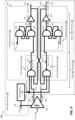
- FIG. 4 is a schematic block diagram illustrating an exemplary SAR ADC portion 400 that implements probabilistic error detection and elimination, according to some embodiments of the present disclosure.
- the SAR ADC portion 400 may correspond to a portion of the SAR ADC 100 of FIG. 1 , where the SAR logic circuitry 430 may replace the SAR logic circuitry 130 shown in FIG. 1 and/or FIG. 2 .
- the SAR ADC portion 400 shares many elements with the SAR ADC portion 200 of FIG. 2 ; for brevity, a discussion of these elements is not repeated, and these elements may take the form of any of the embodiments disclosed herein.
- the SAR logic circuitry 430 may include a shift register 210, a first digital path 401, and a second digital path 403.
- the first digital path 401 may be coupled to the positive output terminal (shown by the symbol "+") of the comparator 120 and the output of the shift register 210.
- the second digital path 403 may be coupled to the negative output terminal (shown by the symbol "-") of the comparator 120 and the output of the shift register 210.
- the SAR logic circuitry 430 may further include first logic circuitry 410 and second logic circuitry 420 downstream of the first logic circuitry 410.
- the first logic circuitry 410 may include first gating circuitry 412 in the first digital path 401 and second gating circuitry 414 in the second digital path 403.
- the second logic circuitry 420 may include latching circuitry 230 and buffer gate 250 in the first digital path 401 and latching circuitry 240 and buffer gate 252 in the second digital path 403.
- the SAR logic circuitry 430 is illustrated with circuitries (e.g., the first gating circuitry 412 and the second gating circuitry 414, the latching circuitries 230 and 240, and the buffer gates 250 and 252) for generating one bit.
- the SAR logic circuitry 430 can include similar circuitries (e.g., the first logic circuitry 410 and the second logic circuitry 420) for each bit. That is, to provide an ADC resolution of N bits, the SAR logic circuitry 430 may include N number of the circuitries (e.g., the first logic circuitry 410 and the second logic circuitry 420) arranged as shown.
- the SAR logic circuitry 430 may include asynchronous clock generation circuitry similar to the asynchronous clock generation circuitry 260 coupled to the outputs 202 and 204 of the comparator 120 and may generate the comparator output clock signal 132 CLKC and the shift register output clock pulses 212 CLKS as discussed above with reference to FIG. 2 . Further still, the SAR logic circuitry 430 can include any suitable number of latching stages, buffering stages, and/or inverting stages in the first digital path 401 downstream of the first gating circuitry 412 and/or in the second digital path 403 downstream of the second gating circuitry 414.
- the first gating circuitry 412 and the second gating circuitry 414 may detect and eliminate the probabilistic errors discussed above with reference to FIGS. 2 and 3 .
- the first gating circuitry 412 may be coupled to the positive output terminal of the comparator 120, the output of the shift register 210, and the output of the second logic circuitry 420 to receive the positive output 202, a shift register output clock pulse 212, and a digital feedback 402, respectively.
- the digital feedback 402 may include information associated with an opposite polarity of the positive output 202. As shown, the digital feedback 402 may correspond to the output of the buffer gate 252 on the second digital path 403 (coupled to the negative output terminal of the comparator 120).
- the second gating circuitry 414 may be coupled to the negative output terminal of the comparator 120, the output of the shift register 210, and the output of the second logic circuitry 420 to receive the negative output 204, the shift register output clock pulse 212, and a digital feedback 404, respectively.
- the digital feedback 404 may include information associated with an opposite polarity of the negative output 204. As shown, the digital feedback 404 may correspond to the output of the buffer gate 250 on the first digital path 401 (coupled to the positive output terminal of the comparator 120).
- the digital feedback 402 may be taken from any node subsequent to reset circuitry (e.g., the latching circuitry 240 with the reset Q rstb ) on the second digital path 403, and the digital feedback 404 may be taken from any node subsequent to reset circuitry (e.g., the latching circuitry 230 with the reset Q rstb ) on the first digital path 401.
- reset circuitry e.g., the latching circuitry 240 with the reset Q rstb
- the digital feedback 404 may be taken from any node subsequent to reset circuitry (e.g., the latching circuitry 230 with the reset Q rstb ) on the first digital path 401.
- a probabilistic error (or a forbidden state) may occur when the shift register output clock pulse 212 (e.g., CLKS ⁇ 10>) for the previous bit trial remains active after the comparison for the current bit trial is completed and the comparison result for the current bit trial is opposite of the comparison result for the previous bit trial.
- the first gating circuitry 412 may utilize the digital feedback 402 to detect whether the forbidden state has occurred and gate the positive output 202 to the second logic circuitry 420 upon detecting the forbidden state.
- the second gating circuitry 414 may utilize the digital feedback 404 to detect whether the forbidden state has occurred and gate the negative output 204 to the second logic circuitry 420 upon detecting the forbidden state.
- the shift register output clock pulse 212 e.g., CLKS ⁇ 10>
- the first gating circuitry 412 may be implemented using a 3-input NAND gate 413, for example, having a first input to receive a positive output 202, a second input to receive a shift register output clock pulse 212, and a third input to receive information (e.g., the digital feedback 402) associated with an opposite polarity of the positive output 202.
- the second gating circuitry 414 may be implemented using a 3-input NAND gate 415, for example, having a first input to receive a negative output 204, a second input coupled to receive the shift register output clock pulse 212, and a third input to receive information (e.g., the digital feedback 404) associated with an opposite polarity of the negative output 204.
- the addition of the digital feedback 402 as an input to the NAND gate 413 can prevent the SAR logic circuitry 430 from writing to a certain bit in the N-bit value (for a certain bit trial) twice.
- the addition of the digital feedback 404 as an input to the NAND gate 415 can prevent the second gating circuitry 414 from writing to a certain bit in the N-bit value (for a certain bit trial) twice.
- the SAR logic circuitry 430 had already written a comparison result to the downstream second logic circuitry 420 for a certain bit trial, the SAR logic circuitry 430 may not write another comparison result to the downstream second logic circuitry 420.
- the 3-input NAND gate 413 e.g., the first gating circuitry 412
- the 3-input NAND gate 415 e.g., the second gating circuitry 414
- the 3-input NAND gate 413 and the 3-input NAND gate 415 can detect and eliminate the probabilistic error or the forbidden state in the first digital path 401 and the second digital path 403, respectively.
- FIG. 4 illustrates the first gating circuitry 412 implemented using the 3-input NAND gate 413 and the second gating circuitry 414 implemented using the 3-input NAND gate 415
- the first gating circuitry 412 and the second gating circuitry 414 may be implemented using any suitable logics and gates.
- the first logic circuitry 410 may receive a first positive output 202 and a first negative output 204 for a current bit trial (e.g., for b k ).
- the first logic circuitry 410 may gate the first positive output 202 to the second logic circuitry based on an output of the second logic circuitry 420 responsive to a second negative output 204 for a previous bit trial (e.g., for b k-1 ).
- the first logic circuitry 410 may gate the first negative output 204 to the second logic circuitry based on an output of the second logic circuitry 420 responsive to a second positive output 202 for a previous bit trial (e.g., for b k-1 ).
- FIG. 5 is discussed in relation to FIGS. 2 and 4 to illustrate the benefits of utilizing the digital feedbacks 402 and 404 in the SAR logic circuitry 430.
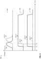
- FIG. 5 is a timing diagram 500 illustrating SAR ADC control signals and bit signals with and without probabilistic error detection and elimination, according to some embodiments of the present disclosure.
- the x-axes may represent timing in some constant units
- the y-axes may represent voltages in some constant units.
- the graph 502 illustrates exemplary curves 510 and 512 corresponding to the shift register output clock pulses 212.
- the curves 510 (shown by the solid line) and 512 (shown by the dashed line) may correspond to CLKS ⁇ 10> for bit 10 (e.g., b 10 ) and CLKS ⁇ 9> for bit 9 (e.g., bg), respectively, of a 11-bit test value (e.g., [b 10 , ..., b 0 ]) for bit trials in the SAR logic circuitry 130 of FIGS. 1 and 2 and/or the SAR logic circuitry 430 of FIG. 4 , respectively.
- a 11-bit test value e.g., [b 10 , ..., b 0 ]
- the graph 504 illustrates exemplary curves 520 (shown by the solid line) and 522 (shown by the dashed line) corresponding to the output 251 dpb ⁇ 10> (for bit 10 responsive to the comparator 120's positive output 202 C op ) and the output 253 dnb ⁇ 10> (for bit 10 responsive to the comparator 120's negative output 204 C on ), respectively, generated by the SAR logic circuitry 130 of FIG. 2 .
- the graph 506 illustrates exemplary curves 530 (shown by the solid line) and 532 (shown by the dashed line) corresponding to the output 251 dpb ⁇ 10> (for bit 10 responsive to the comparator 120's positive output 202 C op ) and the output 253 dnb ⁇ 10> (for bit 10 responsive to the comparator 120's negative output 204 C on ), respectively, generated by the SAR logic circuitry 430 of FIG. 4 .
- the comparator output clock signal 132 is not shown.
- the shift register 210 may be clocked by the comparator output clock signal 132 to generate the shift register output clock pulses CLK ⁇ 10> and CLK ⁇ 9> and the comparator 120 may be clocked by the comparator output clock signal 132 to generate C op and C on as discussed above with reference to FIGS. 2-4 .
- both C op and C on are logic low, for example, after the SAR logic circuitry 130 is reset where bit 10 of the test value is set to 1 and all other bits of the test value are set to 0, and the switches for the capacitors in the DAC 116 are configured according to the test value.
- the comparator 120 may complete comparing a sampled input voltage (e.g., an analog input voltage 102 sampled by the S/H circuitry 112) to a first DAC output voltage (e.g., generated by the DAC 116 with bit 10 set to 1 and all other bits set to 0) and may generate a comparison result for bit 10. As an example, the comparator 120 may determine that the sampled input voltage is greater than the first DAC output voltage.
- a sampled input voltage e.g., an analog input voltage 102 sampled by the S/H circuitry 112
- a first DAC output voltage e.g., generated by the DAC 116 with bit 10 set to 1 and all other bits set to 0
- the SAR logic circuitry 130 may output a logic high for dpb ⁇ 10> and a logic low for dnb ⁇ 10> as shown by the graph 504, where the curve 520 for dpb ⁇ 10> transitions to a logic high and the curve 522 for dnb ⁇ 10> remains a logic low.
- the SAR logic circuitry 430 may output a logic high for dpb ⁇ 10> and a logic low for dnb ⁇ 10> as shown by the graph 506, where the curve 530 for dpb ⁇ 10> transitions to a logic high and the curve 532 for dnb ⁇ 10> remains a logic low.
- the SAR logic circuitry 430 may keep the logic 1 for bit 10 in the test value based on the comparison result and set bit 9 to a 1 for a next bit trial for bit 9.
- the comparator 120 may complete comparing the sampled input voltage to a second DAC output voltage (e.g., generated by the DAC 116 with bit 10 remains as 1 and bit 9 updated to 1) and may generate a comparison result for bit 9.
- the comparator 120 may determine that the sampled input voltage is smaller than the second DAC output voltage.
- CLKS ⁇ 10> remains active (e.g., at time T2 due to the rounding or slowing of the clock edges) after the comparison result for bit 9 is ready.
- the SAR logic circuitry 130 may incorrectly write the comparison result for bit 9 to the output 253 (e.g., dnb ⁇ 10>) again for bit 10 based on CLKS ⁇ 10> being asserted as shown by the graph 504, where the curve 522 for dnb ⁇ 10> transitions to a logic high at time T2.
- having the same bit written twice with a logic 1 value can cause not only bit 10 to be in error, but all subsequent bits to be erroneous as well.
- the SAR logic circuitry 430 may not write the comparison result for bit 9 to the output 253 (e.g., dnb ⁇ 10>) again for bit 10 even though CLKS ⁇ 10> remains asserted when the comparison result for bit 9 is ready as shown by the graph 504, where the curve 532 for dnb ⁇ 10> remains a logic low at time T2.
- gating the comparator 120's positive output 202 C op and negative output 204 C on to a next downstream logic circuitry e.g., the second logic circuitry 420
- respective opposite polarity information e.g., the digital feedback 402 for the positive output 202 and the digital feedback 404 for the negative output 204 can advantageously detect and eliminate the probabilistic error or the forbidden state.
- FIG. 6 is a schematic block diagram illustrating an exemplary SAR ADC portion 600 that implements probabilistic error detection and elimination, according to some embodiments of the present disclosure.
- the SAR ADC portion 600 may correspond to a portion of the SAR ADC 100 of FIG. 1 , where the SAR logic circuitry 630 may replace the SAR logic circuitry 130 shown in FIG. 1 and/or FIG. 2 to provide probabilistic error detection and elimination.
- the SAR ADC portion 600 shares many elements with the SAR ADC portion 400 of FIG. 4 ; for brevity, a discussion of these elements is not repeated, and these elements may take the form of any of the embodiments disclosed herein.
- the SAR ADC portion 600 may include SAR logic circuitry 630 coupled to the comparator 120 in the same way as the SAR logic circuitry 430 of FIG. 4 .
- the SAR logic circuitry 630 may have similar internal components and connections as the SAR logic circuitry 430, but the latching circuitries 230 and 240 are implemented using D flip-flops instead of SR flip-flops as in FIG. 4 .
- the latching circuitry 230 is implemented using a D flip-flop 632 including an input shown by "D" (which may be referred to as a D input), a clock input shown by the triangle symbol, and an output shown by "Q" (which may be referred to as a Q output).
- the D input of the D flip-flop 632 is connected to a logic 1 or logic high (shown as HI), the clock input of the D flip-flop 632 is coupled to the output 416 of the first gating circuitry 412 and the Q output 635 is coupled to the buffer gate 250.
- the latching circuitry 240 is implemented using a D flip-flop 642 including a D input connected to a logic high, a clock input coupled to the output 417 of the second gating circuitry 414, and a Q output 645 coupled to the buffer 252.
- the latching circuitry 230 and the latching circuitry 240 may be implemented using any suitable gates and logic circuitry (e.g., transistors) configured to latch or clock an input of the circuitry to the output of the circuitry.
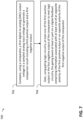
- FIG. 7 is a flow diagram illustrating an exemplary method 700 for performing for SAR ADC operations, according to some embodiments of the present disclosure.
- the method 700 can be implemented by a SAR ADC (e.g., the SAR ADC 100, the SAR ADC portion 200, 400, and/or 600).
- the method 700 may utilize similar mechanisms as discussed above with reference to FIGS. 1-6 .
- the operations of the method 700 may be illustrated with reference to particular embodiments of the SAR ADC disclosed herein, the method 700 may be performed using any suitable hardware components and/or software components. Operations are illustrated once each and in a particular order in FIG. 7 , but the operations may be performed in parallel, reordered, and/or repeated as desired.
- a first DAC output voltage may be compared to a sampled analog input voltage using a comparator (e.g., the comparator 120) to generate a comparison result including a first positive output and a first negative output.
- a comparator e.g., the comparator 120
- the first DAC output voltage, the sampled analog input voltage, the first positive output, and the first negative output may correspond to the DAC output voltage 117, the sampled analog input voltage 113, the positive output 202, and the negative output 204, respectively.
- the first DAC output voltage may be generated using a switched capacitor DAC (e.g., the switched capacitor DAC 116) based on a digital output code.
- At 704 at least one of the first positive output or the first negative output of the comparator may be gated to next logic circuitry using gating logic circuitry (e.g., the gating circuitries 412 and/or 414).
- the gating may be based at least in part on a digital feedback (e.g., the digital feedback 402 or 404) including information associated with at least one of an opposite polarity of the first positive output or an opposite polarity of the first negative output.
- the digital feedback may include an output of the next logic circuitry, where the output may be responsive to at least one of a second positive output or a second negative output of the comparator.
- the first positive output and the first negative output may be a comparison result for a current bit trial (e.g., for bit k), and the second positive output and the second negative output may be for a previous bit trial (e.g., for bit k-1).
- the gating at 704 may include gating the first positive output (e.g., C op ⁇ k>) of the comparator to the next logic circuitry further based on the output (e.g., dnb ⁇ k-1>) responsive to the second negative output (e.g., C on ⁇ k-1>) of the comparator having a logic one value and the first positive output of the comparator having a logic one value.
- the first positive output e.g., C op ⁇ k>
- the next logic circuitry further based on the output (e.g., dnb ⁇ k-1>) responsive to the second negative output (e.g., C on ⁇ k-1>) of the comparator having a logic one value and the first positive output of the comparator having a logic one value.
- the gating may include gating the first negative output (e.g., C on ⁇ k>) of the comparator to the next logic circuitry further based on the output (e.g., dpb ⁇ k-1>) responsive to the second positive output (e.g., C op ⁇ k-1>) of the comparator having a logic one value and the first negative output of the comparator having a logic one value.
- the first negative output e.g., C on ⁇ k>
- the next logic circuitry further based on the output (e.g., dpb ⁇ k-1>) responsive to the second positive output (e.g., C op ⁇ k-1>) of the comparator having a logic one value and the first negative output of the comparator having a logic one value.
- the gating at 704 may be further based on a detection of a shift register output clock pulse (e.g., the shift register output clock pulse 212 CLKS ⁇ k-1>) associated with the previous bit trial (e.g., for bit k-1) remaining active after the comparator generated the first positive output and the first negative output (for the current bit trial for bit k), for example, as shown in the graph 304 of FIG. 3 and/or the graph 502 of FIG. 5 .
- the method 700 may further include comparing a second DAC output voltage to the sampled analog input voltage to generate the second positive output and the second negative output and transmitting the second positive output and the second negative output to the next logic circuitry during the shift register output clock pulse.
- the comparing the second DAC output voltage to the sampled analog input voltage (for the previous bit trial) may be triggered in response to a first comparator clock pulse (e.g., the comparator output clock 132 CLKC ⁇ k-1>).
- the shift register output clock pulse may be triggered also in response to the same first comparator clock pulse.
- the comparing the first DAC output voltage to the sampled analog input voltage (for the current bit trial) may be triggered in response to a second comparator clock pulse (e.g., the comparator output clock 132 CLKC ⁇ k>) after the first clock pulse.
- the method 700 may further include resetting the comparator and the next logic circuitry after the previous bit trial.
- Example 1 include a method for performing successive approximation registers (SAR) analog-to-digital conversion.
- the method includes comparing, using a comparator, a first digital-to-analog (DAC) output voltage to a sampled analog input voltage to generate a comparison result including a first positive output and a first negative output; and gating, using gating logic circuitry, at least one of the first positive output or the first negative output of the comparator to next logic circuitry, the gating based at least in part on a digital feedback including information associated with at least one of an opposite polarity of the first positive output or an opposite polarity of the first negative output.
- SAR successive approximation registers
- Example 2 the subject matter of Example 1 can optionally include where the digital feedback includes an output of the next logic circuitry, the output responsive to at least one of a second positive output or a second negative output of the comparator.
- Example 3 the subject matter of any of Examples 1-2 can optionally include where the gating includes gating the first positive output of the comparator to the next logic circuitry further based on the output responsive to the second negative output of the comparator having a logic one value and the first positive output of the comparator having a logic one value.
- Example 4 the subject matter of any of Examples 1-3 can optionally include where the gating includes gating the first negative output of the comparator to the next logic circuitry further based on the output responsive to the second positive output of the comparator having a logic one value and the first negative output of the comparator having a logic one value.
- Example 5 the subject matter of any of Examples 1-4 can optionally include where the first positive output and the first negative output of the comparator are associated with a current bit trial; and the at least one of the second positive output or the second negative output of the comparator are associated with a previous bit trial.
- Example 6 the subject matter of any of Examples 1-5 can optionally include where the gating is further based on a detection of a shift register output clock pulse associated with the previous bit trial remaining active after the comparator generated the first positive output and the first negative output.
- Example 7 The method any of Examples 1-6 can optionally include comparing a second DAC output voltage to the sampled analog input voltage to generate the second positive output and the second negative output for the previous bit trial; and transmitting, during the shift register output clock pulse, the second positive output and the second negative output to the next logic circuitry.
- Example 8 the subject matter of any of Examples 1-7 can optionally include where the comparing the second DAC output voltage to the sampled analog input voltage is triggered in response to a first comparator clock pulse; the shift register output clock pulse is triggered in response to the first comparator clock pulse; and the comparing the first DAC output voltage to the sampled analog input voltage is triggered in response to a second comparator clock pulse after the first comparator clock pulse.
- Example 9 the subject matter of any of Examples 1-8 can optionally include resetting the comparator and the next logic circuitry after the previous bit trial.
- Example 10 the subject matter of any of Examples 1-9 can optionally include generating, using a switched capacitor digital-to-analog converter (DAC), the first DAC output voltage based on a digital output code.
- DAC switched capacitor digital-to-analog converter
- Example 11 includes a successive approximation registers (SAR) analog-to-digital converter (ADC) including a digital-to-analog converter (DAC) to generate a first DAC output voltage based on a digital output code associated with an analog input voltage; a comparator to compare the first DAC output voltage to the analog input voltage to generate a comparison result including a first positive output and first negative output; and SAR logic circuitry including first logic circuitry to gate, based at least in part on a digital feedback, at least one of the first positive output or the first negative output of the comparator to second logic circuitry, the digital feedback including information associated with at least one of an opposite polarity of the a first positive output or an opposite polarity of the first negative output; and the second logic circuitry downstream of the first logic circuitry.
- SAR successive approximation registers
- ADC analog-to-digital converter
- DAC digital-to-analog converter
- Example 12 the subject matter of Example 11 can optionally include where the digital feedback includes an output of the second logic circuitry, the output responsive to at least one of a second positive output or a second negative output of the comparator.
- Example 13 the subject matter of any of Examples 11-12 can optionally include where the first positive output and the first negative output of the comparator are associated with a current bit trial; and the at least one of a second positive output or a second negative output of the comparator is associated with a previous bit trial.
- Example 14 the subject matter of any of Examples 11-13 can optionally include where the first logic circuitry further gates the at least one of the first positive output or the first negative output of the comparator to the second logic circuitry based on a detection of a shift register output clock pulse associated with the previous bit trial remaining active after the comparator generated the first positive output and the first negative output.
- Example 15 the subject matter of any of Examples 11-14 can optionally include where the comparator further compares a second DAC output voltage to the analog input voltage to generate the second positive output and the second negative output for the previous bit trial; and the first logic circuitry further transmits, during the shift register output clock pulse, the second positive output and the second negative output to the second logic circuitry.
- Example 16 the subject matter of any of Examples 11-15 can optionally include where the comparator compares the second DAC output voltage to the analog input voltage responsive to a first comparator clock pulse associated with the previous bit trial; the comparator compares the first DAC output voltage to the analog input voltage responsive to a second comparator clock pulse associated with the current bit trial; and the SAR logic circuitry further includes a shift register to generate the shift register output clock pulse responsive to the first comparator clock pulse.
- Example 17 the subject matter of any of Examples 11-16 can optionally include asynchronous clock generation circuitry to generate the first comparator clock pulse for the previous bit trial; and generate, responsive to a completion of the previous bit trial, the second comparator clock pulse for the current bit trial.
- Example 18 the subject matter of any of Examples 11-17 can optionally include where the first logic circuitry includes NOT-AND (NAND) circuitry to receive the first positive output or the first negative output of the comparator, the digital feedback, and a shift register output clock pulse.
- the first logic circuitry includes NOT-AND (NAND) circuitry to receive the first positive output or the first negative output of the comparator, the digital feedback, and a shift register output clock pulse.
- NAND NOT-AND
- Example 19 the subject matter of any of Examples 11-18 can optionally include where the second logic circuitry includes reset circuitry, and where the digital feedback corresponds to an output downstream of the reset circuitry.
- Example 20 the subject matter of any of Examples 11-19 can optionally include where the DAC includes a switched capacitor DAC.
- Example 21 includes a successive approximation registers (SAR) analog-to-digital converter (ADC) including an analog input to receive an analog input voltage; sample-and-hold circuitry coupled to the analog input; a digital-to-analog converter (DAC); a comparator coupled to an output of the sample-and-hold circuitry and an output of the DAC; and SAR logic circuitry including a shift register; a first digital path including first detection circuitry to receive one of a positive output or a negative output of the comparator, an output of the shift register, and a first digital feedback associated with a second digital path; and the second digital path including second detection circuitry to receive the other one of the positive output or the negative output of the comparator, the output of the shift register, and a second digital feedback associated with the first digital path.
- SAR successive approximation registers
- ADC analog-to-digital converter
- ADC analog-to-digital converter
- ADC analog-to-digital converter
- ADC analog-to-digital converter
- Example 22 the subject matter of Example 21 can optionally include where the first digital path further includes latching circuitry coupled to an output of the first detection circuitry, and where the second digital feedback corresponds to an output downstream of the latching circuitry.
- Example 23 the subject matter of any of Examples 21-22 can optionally include where the first detection circuitry gates the one of the positive output or the negative output of the comparator to the latching circuitry responsive to the first digital feedback.
- Example 24 The SAR ADC any of Examples 21-23 can optionally include where the first detection circuitry includes a NOT-AND (NAND) gate having a first input to receive the one of the positive output or the negative output of the comparator; a second input to receive the output of the shift register; and a third input to receive the first digital feedback.
- NAND NOT-AND
- Example 25 the subject matter of any of Examples 21-24 can optionally include further including asynchronous clock generation circuitry to provide a comparator clock pulse to the comparator and the shift register.
- Example 26 the subject matter of any of Examples 21-25 can optionally include where the DAC includes a switched capacitor DAC.
- the features discussed herein can be applicable to automotive systems, safety-critical industrial applications, medical systems, scientific instrumentation, wireless and wired communications, radio, radar, industrial process control, audio and video equipment, current sensing, instrumentation (which can be highly precise), and other digital-processing-based systems.
- components of a system such as comparator, DAC, S/H circuitry, shift register, NAND gates, SR flip flops, buffer gates, and/or other components can readily be replaced, substituted, or otherwise modified in order to accommodate particular circuitry needs.
- components of a system such as comparator, DAC, S/H circuitry, shift register, NAND gates, SR flip flops, buffer gates, and/or other components can readily be replaced, substituted, or otherwise modified in order to accommodate particular circuitry needs.
- complementary electronic devices, hardware, software, etc. offer an equally viable option for implementing the teachings of the present disclosure related to SAR ADCs, in various communication systems.
- Parts of various systems for implementing SAR ADCs as proposed herein can include electronic circuitry to perform the functions described herein.
- one or more parts of the system can be provided by a processor specially configured for carrying out the functions described herein.
- the processor may include one or more application specific components, or may include programmable logic gates which are configured to carry out the functions describe herein.
- the circuitry can operate in analog domain, digital domain, or in a mixed-signal domain.
- the processor may be configured to carrying out the functions described herein by executing one or more instructions stored on a non-transitory computer-readable storage medium.
- any number of electrical circuits of the present figures may be implemented on a board of an associated electronic device.
- the board can be a general circuit board that can hold various components of the internal electronic system of the electronic device and, further, provide connectors for other peripherals. More specifically, the board can provide the electrical connections by which the other components of the system can communicate electrically.
- Any suitable processors (inclusive of DSPs, microprocessors, supporting chipsets, etc.), computer-readable non-transitory memory elements, etc. can be suitably coupled to the board based on particular configuration needs, processing demands, computer designs, etc.
- Other components such as external storage, additional sensors, controllers for audio/video display, and peripheral devices may be attached to the board as plug-in cards, via cables, or integrated into the board itself.
- the functionalities described herein may be implemented in emulation form as software or firmware running within one or more configurable (e.g., programmable) elements arranged in a structure that supports these functions.
- the software or firmware providing the emulation may be provided on non-transitory computer-readable storage medium comprising instructions to allow a processor to carry out those functionalities.
- the electrical circuits of the present figures may be implemented as stand-alone modules (e.g., a device with associated components and circuitry configured to perform a specific application or function) or implemented as plug-in modules into application specific hardware of electronic devices.
- SOC system on chip
- An SOC represents an IC that integrates components of a computer or other electronic system into a single chip. It may contain digital, analog, mixed-signal, and often RF functions: all of which may be provided on a single chip substrate.
- Other embodiments may include a multi-chip-module (MCM), with a plurality of separate ICs located within a single electronic package and configured to interact closely with each other through the electronic package.
- MCM multi-chip-module
- references to various features e.g., elements, structures, modules, components, steps, operations, characteristics, etc.
- references to various features e.g., elements, structures, modules, components, steps, operations, characteristics, etc.
- references to various features are intended to mean that any such features are included in one or more embodiments of the present disclosure, but may or may not necessarily be combined in the same embodiments.
- the term “connected” means a direct electrical connection between the things that are connected, without any intermediary devices/components
- the term “coupled” means either a direct electrical connection between the things that are connected, or an indirect connection through one or more passive or active intermediary devices/components
- the term “circuit” means one or more passive and/or active components that are arranged to cooperate with one another to provide a desired function.
- the terms “substantially,” “approximately,” “about,” etc. may be used to generally refer to being within +/- 20% of a target value, e.g., within +/- 10% of a target value, based on the context of a particular value as described herein or as known in the art.
Landscapes
- Engineering & Computer Science (AREA)
- Theoretical Computer Science (AREA)
- Power Engineering (AREA)
- Analogue/Digital Conversion (AREA)
Abstract
Description
- The present disclosure generally relates to electronics, and, more specifically, to successive approximation register (SAR) analog-to-digital converters (ADCs).
- In many electronics applications, an analog input signal is converted to a digital output signal (e.g., for further digital signal processing). For instance, in precision measurement systems, electronics are provided with one or more sensors to make measurements, and these sensors can generate an analog signal. The analog signal can then be provided to an analog-to-digital converter (ADC) circuit as input to generate a digital output signal for further processing. In another instance, in a wireless communication device receiver or a base station receiver, an antenna can generate an analog signal based on the electromagnetic waves carrying information/signals in the air. The analog signal generated by the antenna can then be provided as input to an ADC to generate a digital output signal for further processing.
- To provide a more complete understanding of the present disclosure and features and advantages thereof, reference is made to the following description, taken in conjunction with the accompanying figures, wherein like reference numerals represent like parts, in which:
-
FIG. 1 is a schematic block diagram illustrating an exemplary successive approximation register (SAR) analog-to-digital converter (ADC); -
FIG. 2 is a schematic block diagram illustrating an exemplary SAR ADC portion, according to some embodiments of the present disclosure; -
FIG. 3 is a timing diagram illustrating a probabilistic error in a SAR ADC, according to some embodiments of the present disclosure; -
FIG. 4 is a schematic block diagram illustrating an exemplary SAR ADC portion that implements probabilistic error detection and elimination, according to some embodiments of the present disclosure; -
FIG. 5 is a timing diagram illustrating SAR ADC control signals and bit signals without probabilistic error detection and elimination, according to some embodiments of the present disclosure; -
FIG. 6 is a schematic block diagram illustrating an exemplary SAR ADC portion that implements probabilistic error detection and elimination, according to some embodiments of the present disclosure; and -
FIG. 7 is a flow diagram illustrating an exemplary method for performing SAR ADC operations, according to some embodiments of the present disclosure. - The systems, methods, and devices of this disclosure each have several innovative embodiments, no single one of which is solely responsible for all of the desirable attributes disclosed herein. Details of one or more implementations of the subject matter described in this specification are set forth in the description below and the accompanying drawings.
- There are various types of ADC architectures, such as successive approximation (SAR) ADC, sigma-delta ADC, pipelined ADC, and flash ADC. Of the various types of ADC architectures, the SAR ADC has long been favored in many applications requiring high speed, low power consumption, and suitably high conversion resolution. A SAR ADC may implement a binary search algorithm to convert an analog input voltage into a digital code (e.g., an N-bit value). To perform the binary search, the SAR ADC may perform successive comparisons of an analog input voltage to a series of analog test voltages (e.g., digitally-controlled test voltages) and using the result from each comparison to generate a digital code to represent a magnitude of the analog input voltage. Each comparison may be associated with a different bit within the N-bit digital code value. To that end, the SAR ADC may include sample-and-hold (S/H) circuitry to acquire a sample of the analog input voltage and hold the sampled analog input voltage to a constant value for the successive comparisons, a digital-to-analog-converter (DAC) to generate the analog test voltages, a comparator to compare the sampled analog input voltage to each of the analog test voltages, and SAR logic circuitry (e.g., digital circuitry) to control the generation of the digital code based on each of the comparison results.
- To generate the digital code, the SAR logic circuitry may take the output of the comparator, record a bit value (for the N-bit value) according to the output of the comparator, and using the recorded value to update the DAC for a next iteration of the binary search (or bit trial). In some examples, for each comparison, the comparator may generate two outputs, one for a positive result and another one for a negative result while the SAR logic circuitry may generate the same number of outputs as the conversion resolution (e.g., N bits). To track which one of the comparator's outputs belongs to which bit of the N-bit value, the SAR logic circuitry may utilize a shift register to window the comparator's outputs to the correct SAR logic circuitry output (e.g., setting a value for a bit within the N-bit value). A forbidden (or illegal) state may exist in the SAR logic circuitry in which the same SAR logic output (a bit within the N-bit value) cannot be written to twice as it would cause not only the bit being overwritten to be erroneous but all subsequent bits to be erroneous. As used herein, a bit error in the SAR logic circuitry due to the forbidden state may also be referred to as a probabilistic error.
- The forbidden state may be triggered when the SAR ADC is pushed to operate at a high speed (e.g., with a sampling rate of hundreds of megahertz (MHz)). For instance, when the SAR ADC is clocked at a high speed, the edges of the clock signals and/or the windowing signal (e.g., shift register output) in the SAR logic circuitry can become rounded (e.g., a slow-roll off transition from a logic high to a logic low, or vice versa). There are various techniques that may be used to minimize the occurrences of the forbidden state. For example, the edge rate of the shift register output can be improved using additional circuitry. However, this may only reduce the probability of the forbidden state from occurring and does not eliminate the occurrences of the forbidden state. Further, the additional circuitry can increase cost, power, and/or area for the SAR ADC. In another example, the SAR logic circuitry may utilize flops in the main signal path of the SAR logic circuitry to better gate various circuit decisions. However, flops may have a large propagation delay, and thus may limit the speed at which the SAR logic circuitry can operate. Accordingly, technique improvements for SAR logic circuitry can be beneficial.
- The present disclosure describes mechanisms for providing a high-speed SAR ADC in a manner that can eliminate the probability of SAR logic circuitry from writing a logical value to the same conversion result twice, for example, by logically gating the SAR ADC's comparator outputs using opposite polarity information. That is, the positive output of the comparator may be gated by a digital result associated with a negative output of the comparator, and the negative output of the comparator may be gated by a digital result associated with a positive output of the comparator in a feedback manner. One aspect of the present disclosure provides a SAR ADC including a DAC, a comparator, and SAR logic circuitry. The DAC may generate a first DAC output voltage based on a digital output code (e.g., a test value) associated with an analog input voltage (e.g., a sample analog input voltage). The comparator may compare the first DAC output voltage to the analog input voltage to generate a comparison result including a positive output and a negative output. The SAR logic circuitry may include first logic circuitry and second logic circuitry downstream of the first logic circuitry. The first logic circuitry may gate at least one of the first positive output or the first negative output of the comparator to the second logic circuitry based at least in part on a digital feedback. The digital feedback may include information associated with at least one of an opposite polarity of the first positive output or the first negative output. In some aspects, the second logic circuitry may include latching circuitry and/or reset circuitry, and the digital feedback may correspond to an output downstream of the reset circuitry.
- The first positive output and the first negative output from the comparator may be associated with a current bit trail, and the digital feedback may be associated with a previous bit trial. For instance, the digital feedback may include an output of the second logic circuitry, where the output is responsive to at least one of a second positive output or a second negative output of the comparator. In this regard, for the previous bit trial, the DAC may generate a second DAC output voltage based on a previous digital output code (e.g., a previous test value) associated with the analog input voltage, and the comparator may compare the second DAC output voltage to the analog input voltage to generate a comparison result including the second positive output and the second negative output. In some aspects, as part of the gating, the first logic circuitry may gate the first positive output of the comparator to the second logic circuitry based on the first positive output having a logic one value and the digital feedback indicating the output responsive to the second negative output of the comparator also has a logic one value. In some aspects, as part of the gating, the first logic circuitry may gate the first negative output of the comparator to the second logic circuitry based on the first negative output having a logic one value and the digital feedback indicating the output responsive to the second positive output of the comparator also has a logic one value.
- In some aspects, the SAR logic circuitry may include a shift register that generates output clock pulses, for example, to track the bit position within the digital output code for each bit trial. The occurrences of the forbidden state may be caused by a shift register output clock pulse for a previous bit trial partially overlaps with a shift register output clock pulse for a current bit trial and remains active when the comparator outputs a comparison result for the current bit trial. Accordingly, in some aspects, the gating of the comparator output (e.g., the positive output and the negative output) to the second logic circuitry may be based on a detection of a shift register output clock pulse associated with the previous bit trial remaining active after the comparator generated the first positive output and the first negative output for the current bit trial.
- In some aspects, the first logic circuitry (e.g., the gating circuitry) may include a NOT-AND (NAND) gate with three inputs. For instance, the NAND gate may include a first input to receive the first positive output of the comparator, a second input to receive the digital feedback, and a third input to receive a shift register output clock pulse.
- In some aspects, the SAR logic circuitry may further include asynchronous clock generation circuitry to generate a first comparator clock pulse for the previous bit trial and generate a second comparator clock pulse for the current bit trial, where the second comparator clock pulse may be generated in response to a completion of the previous bit trial.
- The systems, schemes, and mechanisms described herein advantageously enable a SAR ADC to operate at a high speed (e.g., about 100 MHz, 160 MHz, 200 MHz, 220 MHz or more) without the probability of entering a forbidden state. Further, adding the digital feedback circuitry may not increase the SAR logic circuitry complexity, power, area, and/or cost significantly. Accordingly, the disclosed embodiments can provide an efficient and effective solution to eliminate the forbidden state from the SAR logic circuitry. The disclosed SAR ADC may be suitable for use in a wide variety of applications such as audio, wireless communications, instrumentations, energy, health and diagnostic, etc.
-
FIG. 1 is a block diagram illustrating anSAR ADC 100. TheSAR ADC 100 may be used for a broad range of applications, such as audio, communications, energy, healthcare, instrumentation and measurement, motor and power control, industrial automation, and/or aerospace/defense, to convert analog signals to digital values, which can be used for further digital processing. As shown, theSAR ADC 100 may include a switchedcapacitor DAC 110, acomparator 120, andSAR logic circuitry 130. The switchedcapacitor DAC 110 may include S/H circuitry 112, asignal summer 114, and aDAC 116. At a high level, theSAR ADC 100 may receive ananalog input voltage 102 shown as Vin and generate a digital representation (e.g., adigital output code 104 shown as Dout) of theanalog input voltage 102 using a binary search algorithm. TheSAR ADC 100 may be single-ended or differential. That is, theanalog input voltage 102 can be a single-ended voltage (with respect to a ground potential) or a differential voltage. Accordingly, the components of theSAR ADC 100 can be single-ended or differential. - The operations of the
SAR ADC 100 may include a sampling phase followed by a conversion phase. During the sampling phase, the S/H circuitry 112 may acquire or capture a sample of theanalog input voltage 102 and hold the sampled voltage 113 (e.g., a constant value) during the following conversion phase. During the conversion phase, theSAR ADC 100 may perform conversion one bit at a time by performing a binary search. As such, theSAR ADC 100 may perform N number of bit trials to generate an N-bit digital output code 104 (e.g., represented by<bN-1, ..., bo>). To that end, theSAR logic circuitry 130 may begin with setting an N-bit value (e.g., stored in a register) to a midscale. That is, the MSB (e.g., bN-1) of the N-bit value is set to 1 while all other bits of the N-bit value are set to 0. TheDAC 116 may receive the N-bit value and output a first test voltage 117 (e.g., of a series of test voltages 117) according to the N-bit value. As an example, theDAC 116 may be provided with a reference voltage VREF, and thefirst test voltage 117 may correspond to VREF/2 based on the N-bit value having the MSB set to 1 and all other bits set to 0. - The
comparator 120 may compare the sampledvoltage 113 to thefirst test voltage 117 to determine whether the sampled voltage is greater than, or less than thefirst test voltage 117, for example, by subtracting thefirst test voltage 117 from the sampledinput voltage 113 using thesignal summer 114 as shown. In practice, thecomparator 120 may have a positive or non-inverting input terminal and a negative or inverting terminal, where the positive input terminal may be coupled to the output of the S/H circuitry 112 and the negative input terminal may be coupled to the output of theDAC 116. That is, thesignal summer 114 may be implemented as part of thecomparator 120. For the comparison, if the sampledvoltage 113 is greater than thefirst test voltage 117, thecomparator 120 may output a logic high (e.g., a comparison result 122), and theSAR logic circuitry 130 may maintain thelogic 1 for the MSB of the N-bit. If, however, the sampledvoltage 113 is less than thefirst test voltage 117, thecomparator 120 may output a logic low (e.g., a comparison result 122), and theSAR logic circuitry 130 may clear the MBS of the N-bit value to alogic 0. - Subsequently, the
SAR logic circuitry 130 may move on to perform a next bit trial to determine a bit value for the next bit (e.g., bN-2) in the N-bit value in a similar way as for the MSB. For instance, theSAR logic circuitry 130 may set the next bit in the N-bit value to a 1, theDAC 116 may generate a second test voltage 117 (e.g., of a series of test voltages 117) based on the updated N-bit value, thecomparator 120 may compare the sampledvoltage 113 to thesecond test voltage 117, and theSAR logic circuitry 130 may update the N-bit value according to thecomparison result 122 for thesecond test voltage 117. The bit trial process may continue for each subsequent bit of the N-bit value down to the LSB (e.g., b0). Once the last bit trial for the LSB is completed, theSAR logic circuitry 130 may output the N-bit value as thedigital output code 104. - In some aspects, the
DAC 116 may include an array of switched capacitors (e.g., binary-weighted capacitors) connected in parallel, where a first end of each of the capacitors may be selectively coupled to the analog input terminal (where Vin is received), VREF, or GND, and a second, opposite end of each of the capacitors may be coupled to a common terminal. For instance, the first end may be coupled to three switches, each coupled to a different one of the analog input terminal, VREF, or a ground potential (e.g., GND). During the sampling phase, theanalog input voltage 102 may be applied to charge the capacitors, for example, the first end of each of the capacitors may be selectively coupled to the analog input terminal of theSAR ADC 100 to receive theanalog input voltage 102 and the second end of each of the capacitors may be selectively coupled to the common terminal. The capacitors may be charged to a voltage substantially equal to theanalog input voltage 102. After sampling, connections of the capacitors are switched, for example, the first end of each of the capacitors may be selectively coupled to VREF or GND, and the second end may remain coupled to the common terminal. The connections or switches may be controlled using a digital code (e.g., the N-bit value stored in the register) from theSAR logic circuitry 130. Based on the settings or states (open/close) of the switches, theDAC 116 may generate atest voltage 117 at the common terminal. Thetest voltage 117 at the common terminal may be input to thecomparator 120 for comparison against the sampledvoltage 113. In other words, after each bit trial, theSAR logic circuitry 130 may set the respective bit of the N-bit value based on the output of thecomparator 120, and control the switches or connections of the capacitors by selectively coupling the first end of the capacitor to Vref or GND according to the respective bit value. - As further shown in
FIG. 1 , theSAR ADC 100 may receive an externalADC clock signal 101 that drives the operations of the S/H circuitry 112. The externalADC clock signal 101 may be configured in a variety of ways. In some examples, the externalADC clock signal 101 may control the sampling period and the conversion period of theSAR ADC 100 and the rate at which theSAR ADC 100 samples the analoginput voltage signal 102. The externalADC clock signal 101 may also be provided to theSAR logic circuitry 130. In some instances, theSAR logic circuitry 130 may begin an initial bit trial (e.g., the bit trial for MSB, bN-1) based on theADC clock signal 101, but may generate an asynchronous clock signal 132 (shown as CLKC) internally to latch the output signal of thecomparator 120. As such, theasynchronous clock signal 132 may be referred to as a comparator output clock signal. The generation and operations of the comparatoroutput clock signal 132 and the operations of theSAR logic circuitry 130 are discussed more fully below with reference toFIG. 2 . -
FIG. 2 is a schematic block diagram illustrating an exemplarySAR ADC portion 200, according to some embodiments of the present disclosure. TheSAR ADC portion 200 may correspond to a portion of theSAR ADC 100 ofFIG. 1 and may provide a more detailed view of theSAR logic circuitry 130. As shown inFIG. 2 , theSAR logic circuitry 130 may include ashift register 210, asynchronous clock generation circuitry 260,NAND gates 220 and 222 (each with two inputs), latchingcircuitries buffer gates FIG. 2 , theSAR logic circuitry 130 is illustrated with circuitries (e.g., theNAND gates circuitries buffer gates 250 and 252) for generating one bit. However, theSAR logic circuitry 130 can include similar circuitries (e.g., theNAND gates circuitries buffer gates 250 and 252) for each bit. That is, to provide an ADC resolution of N bits, theSAR logic circuitry 130 may include N number of the circuitry including theNAND gates circuitries buffer gates SAR logic circuitry 130 can include any suitable number of latching stages, buffering stages, and/or inverting stages, connected to each of the comparator outputs 202 and 204. - As explained above, to generate an N-bit
digital output code 104, theSAR logic circuitry 130 may perform N number of bit trials, one for each bit. TheSAR logic circuitry 130 may track the bit position within the N-bit value for each bit trial using theshift register 210. Stated differently, theshift register 210 may correlate or associate a certain comparison to a corresponding bit position within the N-bit value. For instance, theshift register 210 may output a series ofclock pulses 212, one for each bit trial. Theclock signal pulses 212 may be shown as CLKS<N-1:0>, where CLKS<N-1> may represent the clock pulse for the MSB bit trial and CLKS<0> may represent the clock pulse for the LSB bit trial. - The
shift register 210 may be implemented using any suitable gates and logic circuitry and may be clocked or driven by the comparatoroutput clock signal 132. For instance, theshift register 210 may output theclock pulse 212 sequentially from CLKS<N-1> to CLKS<0>, each triggered by an assertion (e.g., a rising edge) of the comparatoroutput clock signal 132. In some examples, theshift register 210 may be implemented using a sequence of flops connected in series and clocked by the comparatoroutput clock signal 132. For instance, theshift register 210 may include N number of flops connected in series, and each flop may be sequentially triggered to generate a shift registeroutput clock pulse 212 by a corresponding clock pulse of the comparatoroutput clock signal 132. - For each bit trial (for a kth within the N-bit value), the
comparator 120 may compare a DAC output voltage VDAC (e.g., atest voltage 117 output by the DAC 116) to a sampled analog input voltage (e.g., the analog input voltage 102) and generate a comparison result. More specifically, thecomparator 120 may output apositive output 202 represented by Cop (e.g., at a positive output terminal shown by the "+" symbol) and anegative output 204 represented by Con (e.g., at a negative output terminal shown by the "-" symbol). Each of thepositive output 202 and thenegative output 204 may be a logic high or a logic low. For instance, a logic high for thepositive output 202 may indicate a bit value of 1 for the respective bit, and a logic high for thenegative output 204 may indicate a bit value of 0 for the respective bit. Because a bit value can only be 1 or 0, one of thepositive output 202 or thenegative output 204 may have a logic high, and the other one of thepositive output 202 or thenegative output 204 may have a logic low under normal operations. That is, thepositive output 202 and thenegative output 204 may be complementary of each other when thecomparator 120 converges to a decision. If both thepositive output 202 and thenegative output 204 are logic high or both thepositive output 202 and thenegative output 204 are logic low, it indicates that thecomparator 120 cannot converge to a decision and the comparison result is erroneous. Thecomparator 120 may latch the comparison result to the output terminals according to the comparatoroutput clock signal 132. In this regard, thecomparator 120 may perform a comparison upon detecting an assertion (e.g., a rising edge) of a clock pulse in the comparatoroutput clock signal 132, for example, by responding to a difference between the sampled voltage and the DAC output voltage VDAC, and may output the comparison result. - As further shown in
FIG. 2 , thepositive output 202 of thecomparator 120 and a respective shift register output clock pulse 212 (e.g., CLKS<k>) may be coupled to the inputs of theNAND gate 220. TheNAND gate 220 may operate as a latch, gating thepositive output 202 to the latchingcircuitry 230 based on the respective shift registeroutput clock pulse 212. For example, theNAND gate 220 may generating anoutput 221 represented by setp<k> for the kth bit (e.g., within setp<N-1:0>) when the respective shift registeroutput clock pulse 212 is asserted (a logic high). In a similar way, thenegative output 204 of thecomparator 120 and the respective shift register output clock pulse 212 (e.g., CLKS<k>) may be coupled to the inputs of theNAND gate 222. TheNAND gate 222 may gate thenegative output 204 to the latchingcircuitry 240 based on the respective shift registeroutput clock pulse 212, for example, by generating anoutput 223 represented by setn<k> for the kth bit (e.g., within setn<N-1:0>) when the respective shift registeroutput clock pulse 212 is asserted. Phrased differently, theNAND gates output clock pulse 212. Accordingly, the shift registeroutput clock pulse 212 may operate to window theoutputs comparator 120 for a particular bit trial. - The latching
circuitry 230 may be coupled to the output of theNAND gate 220. The latchingcircuitry 230 may receive theoutput 221 setp<k> from theNAND gate 220 and lock or retain the bit value of setp<k> until a reset is applied to the latchingcircuitry 230. Similarly, the latchingcircuitry 240 may be coupled to the output of theNAND gate 222. The latchingcircuitry 240 may receive theoutput 223 setn<k> from theNAND gate 222 and lock or retain the bit value of setn<k> until a reset is applied to the latchingcircuitry 240. In the illustrated example of theFIG. 2 , the latchingcircuitry 230 is implemented using a set-reset (SR) flip-flop or including a pair of cross-coupled 2-input NAND gates circuitry 240 is implemented as an SR flip-flop including a pair of cross-coupled 2-input NAND gates - The
buffer gate 250 may be coupled to the output of the latchingcircuitry 230. Thebuffer gate 250 may receive the latched output 235 (corresponding to setp<k>) and pass the output 235 (e.g., with a delay) to theoutput 251 represented by dpb<k> for the kth bit (e.g., within dpb<N-1,0>). Similarly, thebuffer gate 252 may be coupled to the output of the latchingcircuitry 240. Thebuffer gate 252 may receive the latched output 245 (corresponding to setn<k>) and pass the output 245 (e.g., with a delay) to theoutput 253 represented by dnb<k> for the kth bit (e.g., within dnb<N-1,0>). - Based on the
NAND gate 220 operations, setp<k> may be a logic low when the positive output 202 Cop<k> is a logic high and CLKS<k> is asserted (a logic high). Conversely, setp<k> may be a logic high when the positive output 202 Cop<k> is a logic low and CLKS<k> is asserted. Similarly, based on theNAND gate 222 operations, setn<k> may be a logic low when the negative output 204 Con<k> is a logic high and CLKS<k> is asserted. Conversely, setn<k> may be a logic high when the negative output 204 Con<k> is a logic low and CLKS<k> is asserted. The SR flip-flop with theNAND gates NAND gates SAR logic circuitry 130 may update the kth bit in the N-bit value (e.g., the test value) and configure the capacitors in theDAC 116, for example, by selectively switching a capacitor corresponding to the kth bit to VREF or GND, according to theoutput 251 and/or 253. In other examples, theSAR logic circuitry 130 may update the kth bit in the N-bit value (e.g., the test value) and configure the capacitors in theDAC 116 by selectively switching a capacitor corresponding to the kth bit to +VREF or - VREF (e.g., depending on the DAC design) according to theoutput 251 and/or 253. - As explained above, the comparator
output clock signal 132 can be generated internally at theSAR logic circuitry 130. As further shown inFIG. 2 , the asynchronous clock generation circuitry 260 may be coupled to the output terminals of thecomparator 120. The asynchronous clock generation circuitry 260 may receive theoutputs output clock signal 132 based at least in part on theoutputs comparator 120 may be reset, for example, thepositive output 202 and thenegative output 204 may each be cleared to a logic low. Additionally, each of the latchingcircuitry 230 and the latchingcircuitry 240 may be reset, for example, by asserting Qrstb at each of the respective SR flip-flops. After the reset, the asynchronous clock generation circuitry 260 may assert a clock pulse for the comparatoroutput clock signal 132 to begin a new comparison or bit trial. - The assertion of the comparator output clock pulse (a rising edge) may trigger a new comparison output at the
comparator 120. The asynchronous clock generation circuitry 260 may monitor thepositive output 202 and thenegative output 204 of thecomparator 120 to determine when thecomparator 120 has completed the comparison and converge to a decision. Because both thepositive output 202 and thenegative output 204 were cleared to a logic low at reset, the asynchronous clock generation circuitry 260 can detect that thecomparator 120 has converged to a decision when thepositive output 202 transition to a logic high or when thenegative output 204 transition to a logic high. Upon detecting a transition at thepositive output 202 or thenegative output 204 of thecomparator 120, the asynchronous clock generation circuitry 260 may de-assert the comparator output clock pulse. After the comparator output clock pulse is de-asserted, theSAR logic circuitry 130 may reset thecomparator 120outputs circuitries - After a certain reset period, the asynchronous clock generation circuitry 260 may assert another clock pulse for the comparator
output clock signal 132 to trigger a next bit trial. In some instances, theSAR logic circuitry 130 may further include clock edge detection and delay circuitries to control the duration of the reset period and the assertion of the reset signals Qrstb. The timing relationships among the signals (e.g., the comparatoroutput clock signal 132, theshift register output 212, and theoutputs SAR logic circuitry 130 are discussed more fully below with reference toFIG. 3 . - As discussed above, as the speed for SAR ADC increases, the edges of the clock signals may become rounded or too slow, causing errors in the conversion.
FIG. 3 is a timing diagram 300 illustrating a probabilistic error in a SAR ADC (e.g., at the SAR logic circuitry 130), according to some embodiments of the present disclosure. InFIG. 3 , the x-axes may represent timing in some constant units, and the y-axes may represent voltages in some constant units. Thegraph 302 illustrates anexemplary curve 310 corresponding to a comparatoroutput clock signal 132 ofFIG. 1 and/orFIG. 2 . The comparatoroutput clock signal 132 may include a series of clock pulses shown as CLKC<10> to CLKC<7>, for example, for testingbit 10 tobit 7, respectively, within the N-bit value (e.g., a test value) discussed above with reference toFIGS. 1 and2 . As an example, N is 11, and thus bit 10 is the MSB. Thegraph 304 illustratesexemplary curves output clock pulses 212. For example, the curves 320 (shown by the solid line), 322 (shown by the dashed line), 324 (shown by the dotted line), and 326 (shown by the dashed-dotted line) may correspond to CLKS<10>, CLKS<9>, CLKS<8>, and CLKS<7>, respectively. Thegraph 306 illustrates exemplary curves 330 (shown by the solid line) and 332 (shown by the dashed line) corresponding to thecomparator 120's positive output 202 Cop and negative output 204 Con, respectively. - As shown, at time T0, both Cop and Con are logic low, for example, after the
SAR logic circuitry 130 is reset wherebit 10 of the test value is set to 1 and all other bits of the test value are set to 0, and the switches for the capacitors in theDAC 116 are configured according to the test value. At time T1, the asynchronous clock generation circuitry 260 may assert CLKC<10>. Upon assertion of CLKC<10>, thecomparator 120 may compare a sampledinput voltage 113 to a first DAC output voltage (e.g., generated by theDAC 116 withbit 10 set to 1 and all other bits set to 0). After a certain delay, at time T2, thecomparator 120 may output a comparison result forbit 10. In the illustrated example ofFIG. 3 , Cop transitions to a logic high and Con remains a logic low indicating that the sampledinput voltage 113 is greater than the first DAC output voltage. - As explained above, the
shift register 210 is also clocked by the comparatoroutput clock signal 132. As shown in thegraph 304, the shift register output clock pulse CLKS<10> forbit 10 may transition to a logic high (e.g., at about time T1) after a certain delay from the assertion of CLKC<10>. When CLKS<10> is a logic high, theNAND gate 220 may output setp (e.g., alogic 0 corresponding to Cop being a logic high for bit 10) and theNAND gate 222 may output setn (e.g., alogic 1 corresponding to Con being a logic low for bit 10). Subsequently, the outputs setp and setn may be passed downstream to the latchingcircuitries buffer gate 250 may output a logic high for dpb<10> and thebuffer gate 252 may output a low for dnb<10>. Additionally, the switches for the capacitors in theDAC 116 are configured according to the test value (dpb<10> or dnb<10>). For example, the first end of the capacitor, which may be referred to as CAPb10 corresponding to bit 10, may be coupled to VREF based on dpb<10> being alogic 1 and dnb<10> being alogic 0. - At time T3, upon detecting the
comparator 120 has completed the comparison forbit 10, the asynchronous clock generation circuitry 260 may de-assert CLKC<10>. After a certain delay from the de-assertion of CLKC<10>, theSAR logic circuitry 130 may reset Cop and Con to a logic low. At time T4, after a reset period (e.g., a delay 301), the asynchronous clock generation circuitry 260 may assert CLKC<9> for a next bit trial. The comparison forbit 9 may be performed in a similar way as forbit 10. Upon assertion of CLKC<10>, thecomparator 120 may compare a sampledinput voltage 113 to a second DAC output voltage (e.g., generated by theDAC 116 withbit 10 remains as 1 andbit 9 updated to 1). After a certain delay, at time T5, thecomparator 120 may output a comparison result forbit 9. In the illustrated example, Con transitions to a logic high and Cop remains a logic low indicating that the sampledinput voltage 113 is lower than the first DAC output voltage. Similar to the shift register output clock pulse CLKS<10>, based on the assertion of CLKC<9> at time T4, the shift register output clock pulse CLKS<9> forbit 9 may be clocked out (e.g., at about time T5). - As can be seen, the edges of the comparator output clock pulses CLKC<10> to CLKC<7> and the shift register output clock pulses CLKS<10> to CLKS<7> are rounded instead of having a sharp transition from a logic low to a logic high at a rising edge or a sharp transition from a logic high to a logic low at the falling edge. The rounding of the clock edges can be problematic. As can be seen, the shift register output clock pulse CLKS<10> partially overlaps with the CLKS<9>. Because CLKS<10> remains active (a logic high) when the
comparator 120 completed the comparison for bit 9 (as shown by the arrow 308), theNAND gates bit 9, but may write those outputs setp and setn again forbit 10 instead of forbit 9. This may cause not only an error forbit 10, but all subsequent bits may be erroneous. This error may be referred to as a probabilistic error since the occurrence of such an error is probabilistic (as show by the arrow 309) depending on the amount of overlap between CLKS<10> and CLKS<9> in time and the amount of time that takes thecomparator 120 to complete a comparison forbit 9. More specifically, such an error may occur when theSAR logic circuitry 130 in a state (the forbidden state) in which the shift registeroutput clock pulse 212 for the previous bit trial remains active after the comparison for the current bit trial is completed and the comparison result for the current bit trial is opposite of the comparison result for the previous bit trial. - In some instances, the forbidden state can cause a catastrophic failure in the SAR ADC because the switches for the capacitors in the
DAC 116 are controlled by the test value. As discussed above, the first end of the capacitor CAPb10 corresponding to bit 10 may be switched to connect to VREF based on the comparison result forbit 10. That is, a first switch coupling the first end of the capacitor CAPb10 to VREF may be closed. Here, because the comparison result forbit 9 is mistakenly identified as forbit 10 based on CLKS<10> remaining active, theSAR logic circuitry 130 may close a second switch that couples the first end of the capacitor CAPb10 to couple to GND. As such, the capacitor CAPb10 may be shorted in opposite directions, and in some instances, this can cause the SAR ADC to enter an irrecoverable erroneous state. - While various techniques may be applied (e.g., increasing the clock edge rate and/or using flops instead of NAND gates and SR latches to better gate signals) to reduce the probability of such probabilistic errors, such probabilistic errors cannot be eliminated.
- Accordingly, the present application provides techniques and circuitries for detecting and eliminating such probabilistic errors in SAR ADC control logic.
-
FIG. 4 is a schematic block diagram illustrating an exemplarySAR ADC portion 400 that implements probabilistic error detection and elimination, according to some embodiments of the present disclosure. For instance, theSAR ADC portion 400 may correspond to a portion of theSAR ADC 100 ofFIG. 1 , where theSAR logic circuitry 430 may replace theSAR logic circuitry 130 shown inFIG. 1 and/orFIG. 2 . TheSAR ADC portion 400 shares many elements with theSAR ADC portion 200 ofFIG. 2 ; for brevity, a discussion of these elements is not repeated, and these elements may take the form of any of the embodiments disclosed herein. - As shown in
FIG. 4 , theSAR logic circuitry 430 may include ashift register 210, a firstdigital path 401, and a seconddigital path 403. The firstdigital path 401 may be coupled to the positive output terminal (shown by the symbol "+") of thecomparator 120 and the output of theshift register 210. The seconddigital path 403 may be coupled to the negative output terminal (shown by the symbol "-") of thecomparator 120 and the output of theshift register 210. TheSAR logic circuitry 430 may further includefirst logic circuitry 410 andsecond logic circuitry 420 downstream of thefirst logic circuitry 410. Thefirst logic circuitry 410 may includefirst gating circuitry 412 in the firstdigital path 401 andsecond gating circuitry 414 in the seconddigital path 403. Thesecond logic circuitry 420 may include latchingcircuitry 230 andbuffer gate 250 in the firstdigital path 401 and latchingcircuitry 240 andbuffer gate 252 in the seconddigital path 403. - In order not to clutter the drawings provided in
FIG. 4 , theSAR logic circuitry 430 is illustrated with circuitries (e.g., thefirst gating circuitry 412 and thesecond gating circuitry 414, the latchingcircuitries buffer gates 250 and 252) for generating one bit. However, theSAR logic circuitry 430 can include similar circuitries (e.g., thefirst logic circuitry 410 and the second logic circuitry 420) for each bit. That is, to provide an ADC resolution of N bits, theSAR logic circuitry 430 may include N number of the circuitries (e.g., thefirst logic circuitry 410 and the second logic circuitry 420) arranged as shown. Further, theSAR logic circuitry 430 may include asynchronous clock generation circuitry similar to the asynchronous clock generation circuitry 260 coupled to theoutputs comparator 120 and may generate the comparatoroutput clock signal 132 CLKC and the shift registeroutput clock pulses 212 CLKS as discussed above with reference toFIG. 2 . Further still, theSAR logic circuitry 430 can include any suitable number of latching stages, buffering stages, and/or inverting stages in the firstdigital path 401 downstream of thefirst gating circuitry 412 and/or in the seconddigital path 403 downstream of thesecond gating circuitry 414. - In some aspects, the
first gating circuitry 412 and thesecond gating circuitry 414 may detect and eliminate the probabilistic errors discussed above with reference toFIGS. 2 and3 . In this regard, thefirst gating circuitry 412 may be coupled to the positive output terminal of thecomparator 120, the output of theshift register 210, and the output of thesecond logic circuitry 420 to receive thepositive output 202, a shift registeroutput clock pulse 212, and adigital feedback 402, respectively. Thedigital feedback 402 may include information associated with an opposite polarity of thepositive output 202. As shown, thedigital feedback 402 may correspond to the output of thebuffer gate 252 on the second digital path 403 (coupled to the negative output terminal of the comparator 120). In a similar way, thesecond gating circuitry 414 may be coupled to the negative output terminal of thecomparator 120, the output of theshift register 210, and the output of thesecond logic circuitry 420 to receive thenegative output 204, the shift registeroutput clock pulse 212, and adigital feedback 404, respectively. Thedigital feedback 404 may include information associated with an opposite polarity of thenegative output 204. As shown, thedigital feedback 404 may correspond to the output of thebuffer gate 250 on the first digital path 401 (coupled to the positive output terminal of the comparator 120). In general, thedigital feedback 402 may be taken from any node subsequent to reset circuitry (e.g., the latchingcircuitry 240 with the reset Qrstb) on the seconddigital path 403, and thedigital feedback 404 may be taken from any node subsequent to reset circuitry (e.g., the latchingcircuitry 230 with the reset Qrstb) on the firstdigital path 401. - As explained above with reference to
FIG. 3 , a probabilistic error (or a forbidden state) may occur when the shift register output clock pulse 212 (e.g., CLKS<10>) for the previous bit trial remains active after the comparison for the current bit trial is completed and the comparison result for the current bit trial is opposite of the comparison result for the previous bit trial. Thefirst gating circuitry 412 may utilize thedigital feedback 402 to detect whether the forbidden state has occurred and gate thepositive output 202 to thesecond logic circuitry 420 upon detecting the forbidden state. Similarly, thesecond gating circuitry 414 may utilize thedigital feedback 404 to detect whether the forbidden state has occurred and gate thenegative output 204 to thesecond logic circuitry 420 upon detecting the forbidden state. In the illustrated example ofFIG. 4 , thefirst gating circuitry 412 may be implemented using a 3-input NAND gate 413, for example, having a first input to receive apositive output 202, a second input to receive a shift registeroutput clock pulse 212, and a third input to receive information (e.g., the digital feedback 402) associated with an opposite polarity of thepositive output 202. In a similar way, thesecond gating circuitry 414 may be implemented using a 3-input NAND gate 415, for example, having a first input to receive anegative output 204, a second input coupled to receive the shift registeroutput clock pulse 212, and a third input to receive information (e.g., the digital feedback 404) associated with an opposite polarity of thenegative output 204. - The addition of the
digital feedback 402 as an input to theNAND gate 413 can prevent theSAR logic circuitry 430 from writing to a certain bit in the N-bit value (for a certain bit trial) twice. Similarly, the addition of thedigital feedback 404 as an input to theNAND gate 415 can prevent thesecond gating circuitry 414 from writing to a certain bit in the N-bit value (for a certain bit trial) twice. Stated differently, if theSAR logic circuitry 430 had already written a comparison result to the downstreamsecond logic circuitry 420 for a certain bit trial, theSAR logic circuitry 430 may not write another comparison result to the downstreamsecond logic circuitry 420. Accordingly, the 3-input NAND gate 413 (e.g., the first gating circuitry 412) and the 3-input NAND gate 415 (e.g., the second gating circuitry 414) can detect and eliminate the probabilistic error or the forbidden state in the firstdigital path 401 and the seconddigital path 403, respectively. - While
FIG. 4 illustrates thefirst gating circuitry 412 implemented using the 3-input NAND gate 413 and thesecond gating circuitry 414 implemented using the 3-input NAND gate 415, thefirst gating circuitry 412 and thesecond gating circuitry 414 may be implemented using any suitable logics and gates. In general, thefirst logic circuitry 410 may receive a firstpositive output 202 and a firstnegative output 204 for a current bit trial (e.g., for bk). Thefirst logic circuitry 410 may gate the firstpositive output 202 to the second logic circuitry based on an output of thesecond logic circuitry 420 responsive to a secondnegative output 204 for a previous bit trial (e.g., for bk-1). In a similar way, thefirst logic circuitry 410 may gate the firstnegative output 204 to the second logic circuitry based on an output of thesecond logic circuitry 420 responsive to a secondpositive output 202 for a previous bit trial (e.g., for bk-1). -
FIG. 5 is discussed in relation toFIGS. 2 and4 to illustrate the benefits of utilizing thedigital feedbacks SAR logic circuitry 430.FIG. 5 is a timing diagram 500 illustrating SAR ADC control signals and bit signals with and without probabilistic error detection and elimination, according to some embodiments of the present disclosure. InFIG. 5 , the x-axes may represent timing in some constant units, and the y-axes may represent voltages in some constant units. Thegraph 502 illustratesexemplary curves output clock pulses 212. For example, the curves 510 (shown by the solid line) and 512 (shown by the dashed line) may correspond to CLKS<10> for bit 10 (e.g., b10) and CLKS<9> for bit 9 (e.g., bg), respectively, of a 11-bit test value (e.g., [b10, ..., b0]) for bit trials in theSAR logic circuitry 130 ofFIGS. 1 and2 and/or theSAR logic circuitry 430 ofFIG. 4 , respectively. Thegraph 504 illustrates exemplary curves 520 (shown by the solid line) and 522 (shown by the dashed line) corresponding to theoutput 251 dpb<10> (forbit 10 responsive to thecomparator 120's positive output 202 Cop) and theoutput 253 dnb<10> (forbit 10 responsive to thecomparator 120's negative output 204 Con), respectively, generated by theSAR logic circuitry 130 ofFIG. 2 . Thegraph 506 illustrates exemplary curves 530 (shown by the solid line) and 532 (shown by the dashed line) corresponding to theoutput 251 dpb<10> (forbit 10 responsive to thecomparator 120's positive output 202 Cop) and theoutput 253 dnb<10> (forbit 10 responsive to thecomparator 120's negative output 204 Con), respectively, generated by theSAR logic circuitry 430 ofFIG. 4 . In order not to clutter the drawings provided inFIG. 5 , the comparatoroutput clock signal 132 is not shown. However, theshift register 210 may be clocked by the comparatoroutput clock signal 132 to generate the shift register output clock pulses CLK<10> and CLK<9> and thecomparator 120 may be clocked by the comparatoroutput clock signal 132 to generate Cop and Con as discussed above with reference toFIGS. 2-4 . - As shown, at time T0, both Cop and Con are logic low, for example, after the
SAR logic circuitry 130 is reset wherebit 10 of the test value is set to 1 and all other bits of the test value are set to 0, and the switches for the capacitors in theDAC 116 are configured according to the test value. - At time T1, the
comparator 120 may complete comparing a sampled input voltage (e.g., ananalog input voltage 102 sampled by the S/H circuitry 112) to a first DAC output voltage (e.g., generated by theDAC 116 withbit 10 set to 1 and all other bits set to 0) and may generate a comparison result forbit 10. As an example, thecomparator 120 may determine that the sampled input voltage is greater than the first DAC output voltage. Accordingly, theSAR logic circuitry 130 may output a logic high for dpb<10> and a logic low for dnb<10> as shown by thegraph 504, where thecurve 520 for dpb<10> transitions to a logic high and thecurve 522 for dnb<10> remains a logic low. Similarly, theSAR logic circuitry 430 may output a logic high for dpb<10> and a logic low for dnb<10> as shown by thegraph 506, where thecurve 530 for dpb<10> transitions to a logic high and thecurve 532 for dnb<10> remains a logic low. - Subsequently, the
SAR logic circuitry 430 may keep thelogic 1 forbit 10 in the test value based on the comparison result and setbit 9 to a 1 for a next bit trial forbit 9. At time T2, thecomparator 120 may complete comparing the sampled input voltage to a second DAC output voltage (e.g., generated by theDAC 116 withbit 10 remains as 1 andbit 9 updated to 1) and may generate a comparison result forbit 9. As an example, thecomparator 120 may determine that the sampled input voltage is smaller than the second DAC output voltage. - As can be seen from the
curve 510, CLKS<10> remains active (e.g., at time T2 due to the rounding or slowing of the clock edges) after the comparison result forbit 9 is ready. The SAR logic circuitry 130 (without thedigital feedbacks 402 and 404) may incorrectly write the comparison result forbit 9 to the output 253 (e.g., dnb<10>) again forbit 10 based on CLKS<10> being asserted as shown by thegraph 504, where thecurve 522 for dnb<10> transitions to a logic high at time T2. As explained above, having the same bit written twice with alogic 1 value can cause not only bit 10 to be in error, but all subsequent bits to be erroneous as well. - In contrast, the SAR logic circuitry 430 (with the
digital feedbacks 402 and 404) may not write the comparison result forbit 9 to the output 253 (e.g., dnb<10>) again forbit 10 even though CLKS<10> remains asserted when the comparison result forbit 9 is ready as shown by thegraph 504, where thecurve 532 for dnb<10> remains a logic low at time T2. Accordingly, gating thecomparator 120's positive output 202 Cop and negative output 204 Con to a next downstream logic circuitry (e.g., the second logic circuitry 420) by respective opposite polarity information (e.g., thedigital feedback 402 for thepositive output 202 and thedigital feedback 404 for the negative output 204) can advantageously detect and eliminate the probabilistic error or the forbidden state. -
FIG. 6 is a schematic block diagram illustrating an exemplarySAR ADC portion 600 that implements probabilistic error detection and elimination, according to some embodiments of the present disclosure. For instance, theSAR ADC portion 600 may correspond to a portion of theSAR ADC 100 ofFIG. 1 , where theSAR logic circuitry 630 may replace theSAR logic circuitry 130 shown inFIG. 1 and/orFIG. 2 to provide probabilistic error detection and elimination. TheSAR ADC portion 600 shares many elements with theSAR ADC portion 400 ofFIG. 4 ; for brevity, a discussion of these elements is not repeated, and these elements may take the form of any of the embodiments disclosed herein. For instance, theSAR ADC portion 600 may includeSAR logic circuitry 630 coupled to thecomparator 120 in the same way as theSAR logic circuitry 430 ofFIG. 4 . Further, theSAR logic circuitry 630 may have similar internal components and connections as theSAR logic circuitry 430, but the latchingcircuitries FIG. 4 . - As shown in
FIG. 6 , the latchingcircuitry 230 is implemented using a D flip-flop 632 including an input shown by "D" (which may be referred to as a D input), a clock input shown by the triangle symbol, and an output shown by "Q" (which may be referred to as a Q output). The D input of the D flip-flop 632 is connected to alogic 1 or logic high (shown as HI), the clock input of the D flip-flop 632 is coupled to theoutput 416 of thefirst gating circuitry 412 and theQ output 635 is coupled to thebuffer gate 250. Similarly, the latchingcircuitry 240 is implemented using a D flip-flop 642 including a D input connected to a logic high, a clock input coupled to theoutput 417 of thesecond gating circuitry 414, and aQ output 645 coupled to thebuffer 252. In general, the latchingcircuitry 230 and the latchingcircuitry 240 may be implemented using any suitable gates and logic circuitry (e.g., transistors) configured to latch or clock an input of the circuitry to the output of the circuitry. -
FIG. 7 is a flow diagram illustrating anexemplary method 700 for performing for SAR ADC operations, according to some embodiments of the present disclosure. Themethod 700 can be implemented by a SAR ADC (e.g., theSAR ADC 100, theSAR ADC portion method 700 may utilize similar mechanisms as discussed above with reference toFIGS. 1-6 . Although the operations of themethod 700 may be illustrated with reference to particular embodiments of the SAR ADC disclosed herein, themethod 700 may be performed using any suitable hardware components and/or software components. Operations are illustrated once each and in a particular order inFIG. 7 , but the operations may be performed in parallel, reordered, and/or repeated as desired. - At 702, a first DAC output voltage may be compared to a sampled analog input voltage using a comparator (e.g., the comparator 120) to generate a comparison result including a first positive output and a first negative output. In some instances, the first DAC output voltage, the sampled analog input voltage, the first positive output, and the first negative output may correspond to the
DAC output voltage 117, the sampledanalog input voltage 113, thepositive output 202, and thenegative output 204, respectively. In some aspects, the first DAC output voltage may be generated using a switched capacitor DAC (e.g., the switched capacitor DAC 116) based on a digital output code. - At 704, at least one of the first positive output or the first negative output of the comparator may be gated to next logic circuitry using gating logic circuitry (e.g., the
gating circuitries 412 and/or 414). The gating may be based at least in part on a digital feedback (e.g., thedigital feedback 402 or 404) including information associated with at least one of an opposite polarity of the first positive output or an opposite polarity of the first negative output. In some aspects, the digital feedback may include an output of the next logic circuitry, where the output may be responsive to at least one of a second positive output or a second negative output of the comparator. For instance, the first positive output and the first negative output may be a comparison result for a current bit trial (e.g., for bit k), and the second positive output and the second negative output may be for a previous bit trial (e.g., for bit k-1). - In some aspects, the gating at 704 may include gating the first positive output (e.g., Cop<k>) of the comparator to the next logic circuitry further based on the output (e.g., dnb<k-1>) responsive to the second negative output (e.g., Con<k-1>) of the comparator having a logic one value and the first positive output of the comparator having a logic one value. In some aspects, the gating may include gating the first negative output (e.g., Con<k>) of the comparator to the next logic circuitry further based on the output (e.g., dpb<k-1>) responsive to the second positive output (e.g., Cop<k-1>) of the comparator having a logic one value and the first negative output of the comparator having a logic one value.
- In some aspects, the gating at 704 may be further based on a detection of a shift register output clock pulse (e.g., the shift register
output clock pulse 212 CLKS<k-1>) associated with the previous bit trial (e.g., for bit k-1) remaining active after the comparator generated the first positive output and the first negative output (for the current bit trial for bit k), for example, as shown in thegraph 304 ofFIG. 3 and/or thegraph 502 ofFIG. 5 . In some aspects, for the previous bit trial, themethod 700 may further include comparing a second DAC output voltage to the sampled analog input voltage to generate the second positive output and the second negative output and transmitting the second positive output and the second negative output to the next logic circuitry during the shift register output clock pulse. In some aspects, the comparing the second DAC output voltage to the sampled analog input voltage (for the previous bit trial) may be triggered in response to a first comparator clock pulse (e.g., thecomparator output clock 132 CLKC<k-1>). The shift register output clock pulse may be triggered also in response to the same first comparator clock pulse. The comparing the first DAC output voltage to the sampled analog input voltage (for the current bit trial) may be triggered in response to a second comparator clock pulse (e.g., thecomparator output clock 132 CLKC<k>) after the first clock pulse. In some aspects, themethod 700 may further include resetting the comparator and the next logic circuitry after the previous bit trial. - In Example 1 include a method for performing successive approximation registers (SAR) analog-to-digital conversion. The method includes comparing, using a comparator, a first digital-to-analog (DAC) output voltage to a sampled analog input voltage to generate a comparison result including a first positive output and a first negative output; and gating, using gating logic circuitry, at least one of the first positive output or the first negative output of the comparator to next logic circuitry, the gating based at least in part on a digital feedback including information associated with at least one of an opposite polarity of the first positive output or an opposite polarity of the first negative output.
- In Example 2, the subject matter of Example 1 can optionally include where the digital feedback includes an output of the next logic circuitry, the output responsive to at least one of a second positive output or a second negative output of the comparator.
- In Example 3, the subject matter of any of Examples 1-2 can optionally include where the gating includes gating the first positive output of the comparator to the next logic circuitry further based on the output responsive to the second negative output of the comparator having a logic one value and the first positive output of the comparator having a logic one value.
- In Example 4, the subject matter of any of Examples 1-3 can optionally include where the gating includes gating the first negative output of the comparator to the next logic circuitry further based on the output responsive to the second positive output of the comparator having a logic one value and the first negative output of the comparator having a logic one value.
- In Example 5, the subject matter of any of Examples 1-4 can optionally include where the first positive output and the first negative output of the comparator are associated with a current bit trial; and the at least one of the second positive output or the second negative output of the comparator are associated with a previous bit trial.
- In Example 6, the subject matter of any of Examples 1-5 can optionally include where the gating is further based on a detection of a shift register output clock pulse associated with the previous bit trial remaining active after the comparator generated the first positive output and the first negative output.
- In Example 7. The method any of Examples 1-6 can optionally include comparing a second DAC output voltage to the sampled analog input voltage to generate the second positive output and the second negative output for the previous bit trial; and transmitting, during the shift register output clock pulse, the second positive output and the second negative output to the next logic circuitry.
- In Example 8, the subject matter of any of Examples 1-7 can optionally include where the comparing the second DAC output voltage to the sampled analog input voltage is triggered in response to a first comparator clock pulse; the shift register output clock pulse is triggered in response to the first comparator clock pulse; and the comparing the first DAC output voltage to the sampled analog input voltage is triggered in response to a second comparator clock pulse after the first comparator clock pulse.
- In Example 9, the subject matter of any of Examples 1-8 can optionally include resetting the comparator and the next logic circuitry after the previous bit trial.
- In Example 10, the subject matter of any of Examples 1-9 can optionally include generating, using a switched capacitor digital-to-analog converter (DAC), the first DAC output voltage based on a digital output code.
- Example 11 includes a successive approximation registers (SAR) analog-to-digital converter (ADC) including a digital-to-analog converter (DAC) to generate a first DAC output voltage based on a digital output code associated with an analog input voltage; a comparator to compare the first DAC output voltage to the analog input voltage to generate a comparison result including a first positive output and first negative output; and SAR logic circuitry including first logic circuitry to gate, based at least in part on a digital feedback, at least one of the first positive output or the first negative output of the comparator to second logic circuitry, the digital feedback including information associated with at least one of an opposite polarity of the a first positive output or an opposite polarity of the first negative output; and the second logic circuitry downstream of the first logic circuitry.
- In Example 12, the subject matter of Example 11 can optionally include where the digital feedback includes an output of the second logic circuitry, the output responsive to at least one of a second positive output or a second negative output of the comparator.
- In Example 13, the subject matter of any of Examples 11-12 can optionally include where the first positive output and the first negative output of the comparator are associated with a current bit trial; and the at least one of a second positive output or a second negative output of the comparator is associated with a previous bit trial.
- In Example 14, the subject matter of any of Examples 11-13 can optionally include where the first logic circuitry further gates the at least one of the first positive output or the first negative output of the comparator to the second logic circuitry based on a detection of a shift register output clock pulse associated with the previous bit trial remaining active after the comparator generated the first positive output and the first negative output.
- In Example 15, the subject matter of any of Examples 11-14 can optionally include where the comparator further compares a second DAC output voltage to the analog input voltage to generate the second positive output and the second negative output for the previous bit trial; and the first logic circuitry further transmits, during the shift register output clock pulse, the second positive output and the second negative output to the second logic circuitry.
- In Example 16, the subject matter of any of Examples 11-15 can optionally include where the comparator compares the second DAC output voltage to the analog input voltage responsive to a first comparator clock pulse associated with the previous bit trial; the comparator compares the first DAC output voltage to the analog input voltage responsive to a second comparator clock pulse associated with the current bit trial; and the SAR logic circuitry further includes a shift register to generate the shift register output clock pulse responsive to the first comparator clock pulse.
- In Example 17, the subject matter of any of Examples 11-16 can optionally include asynchronous clock generation circuitry to generate the first comparator clock pulse for the previous bit trial; and generate, responsive to a completion of the previous bit trial, the second comparator clock pulse for the current bit trial.
- In Example 18, the subject matter of any of Examples 11-17 can optionally include where the first logic circuitry includes NOT-AND (NAND) circuitry to receive the first positive output or the first negative output of the comparator, the digital feedback, and a shift register output clock pulse.
- In Example 19, the subject matter of any of Examples 11-18 can optionally include where the second logic circuitry includes reset circuitry, and where the digital feedback corresponds to an output downstream of the reset circuitry.
- In Example 20, the subject matter of any of Examples 11-19 can optionally include where the DAC includes a switched capacitor DAC.
- Example 21 includes a successive approximation registers (SAR) analog-to-digital converter (ADC) including an analog input to receive an analog input voltage; sample-and-hold circuitry coupled to the analog input; a digital-to-analog converter (DAC); a comparator coupled to an output of the sample-and-hold circuitry and an output of the DAC; and SAR logic circuitry including a shift register; a first digital path including first detection circuitry to receive one of a positive output or a negative output of the comparator, an output of the shift register, and a first digital feedback associated with a second digital path; and the second digital path including second detection circuitry to receive the other one of the positive output or the negative output of the comparator, the output of the shift register, and a second digital feedback associated with the first digital path.
- In Example 22, the subject matter of Example 21 can optionally include where the first digital path further includes latching circuitry coupled to an output of the first detection circuitry, and where the second digital feedback corresponds to an output downstream of the latching circuitry.
- In Example 23, the subject matter of any of Examples 21-22 can optionally include where the first detection circuitry gates the one of the positive output or the negative output of the comparator to the latching circuitry responsive to the first digital feedback.
- In Example 24.The SAR ADC any of Examples 21-23 can optionally include where the first detection circuitry includes a NOT-AND (NAND) gate having a first input to receive the one of the positive output or the negative output of the comparator; a second input to receive the output of the shift register; and a third input to receive the first digital feedback.
- In Example 25, the subject matter of any of Examples 21-24 can optionally include further including asynchronous clock generation circuitry to provide a comparator clock pulse to the comparator and the shift register.
- In Example 26, the subject matter of any of Examples 21-25 can optionally include where the DAC includes a switched capacitor DAC.
- While embodiments of the present disclosure were described above with references to exemplary implementations as shown in
FIGS. 1-7 , a person skilled in the art will realize that the various teachings described above are applicable to a large variety of other implementations. - In certain contexts, the features discussed herein can be applicable to automotive systems, safety-critical industrial applications, medical systems, scientific instrumentation, wireless and wired communications, radio, radar, industrial process control, audio and video equipment, current sensing, instrumentation (which can be highly precise), and other digital-processing-based systems.
- In the discussions of the embodiments above, components of a system, such as comparator, DAC, S/H circuitry, shift register, NAND gates, SR flip flops, buffer gates, and/or other components can readily be replaced, substituted, or otherwise modified in order to accommodate particular circuitry needs. Moreover, it should be noted that the use of complementary electronic devices, hardware, software, etc., offer an equally viable option for implementing the teachings of the present disclosure related to SAR ADCs, in various communication systems.
- Parts of various systems for implementing SAR ADCs as proposed herein can include electronic circuitry to perform the functions described herein. In some cases, one or more parts of the system can be provided by a processor specially configured for carrying out the functions described herein. For instance, the processor may include one or more application specific components, or may include programmable logic gates which are configured to carry out the functions describe herein. The circuitry can operate in analog domain, digital domain, or in a mixed-signal domain. In some instances, the processor may be configured to carrying out the functions described herein by executing one or more instructions stored on a non-transitory computer-readable storage medium.
- In one example embodiment, any number of electrical circuits of the present figures may be implemented on a board of an associated electronic device. The board can be a general circuit board that can hold various components of the internal electronic system of the electronic device and, further, provide connectors for other peripherals. More specifically, the board can provide the electrical connections by which the other components of the system can communicate electrically. Any suitable processors (inclusive of DSPs, microprocessors, supporting chipsets, etc.), computer-readable non-transitory memory elements, etc. can be suitably coupled to the board based on particular configuration needs, processing demands, computer designs, etc. Other components such as external storage, additional sensors, controllers for audio/video display, and peripheral devices may be attached to the board as plug-in cards, via cables, or integrated into the board itself. In various embodiments, the functionalities described herein may be implemented in emulation form as software or firmware running within one or more configurable (e.g., programmable) elements arranged in a structure that supports these functions. The software or firmware providing the emulation may be provided on non-transitory computer-readable storage medium comprising instructions to allow a processor to carry out those functionalities.
- In another example embodiment, the electrical circuits of the present figures may be implemented as stand-alone modules (e.g., a device with associated components and circuitry configured to perform a specific application or function) or implemented as plug-in modules into application specific hardware of electronic devices. Note that particular embodiments of the present disclosure may be readily included in a system on chip (SOC) package, either in part, or in whole. An SOC represents an IC that integrates components of a computer or other electronic system into a single chip. It may contain digital, analog, mixed-signal, and often RF functions: all of which may be provided on a single chip substrate. Other embodiments may include a multi-chip-module (MCM), with a plurality of separate ICs located within a single electronic package and configured to interact closely with each other through the electronic package.
- It is also imperative to note that all of the specifications, dimensions, and relationships outlined herein (e.g., the number of components of the SAR ADCs shown in
FIGS. 1-2 ,4 , and6 ) have only been offered for purposes of example and teaching only. Such information may be varied considerably without departing from the spirit of the present disclosure, or the scope of the appended claims. It should be appreciated that the system can be consolidated in any suitable manner. Along similar design alternatives, any of the illustrated circuits, components, modules, and elements of the present figures may be combined in various possible configurations, all of which are clearly within the broad scope of this specification. In the foregoing description, example embodiments have been described with reference to particular processor and/or component arrangements. Various modifications and changes may be made to such embodiments without departing from the scope of the appended claims. The description and drawings are, accordingly, to be regarded in an illustrative rather than in a restrictive sense. - Note that with the numerous examples provided herein, interaction may be described in terms of two, three, four, or more electrical components. However, this has been done for purposes of clarity and example only. It should be appreciated that the system can be consolidated in any suitable manner. Along similar design alternatives, any of the illustrated components, modules, and elements of the FIGURES may be combined in various possible configurations, all of which are clearly within the broad scope of this Specification. In certain cases, it may be easier to describe one or more of the functionalities of a given set of flows by only referencing a limited number of electrical elements. It should be appreciated that the electrical circuits of the FIGURES and its teachings are readily scalable and can accommodate a large number of components, as well as more complicated/sophisticated arrangements and configurations. Accordingly, the examples provided should not limit the scope or inhibit the broad teachings of the electrical circuits as potentially applied to a myriad of other architectures.
- Note that in this Specification, references to various features (e.g., elements, structures, modules, components, steps, operations, characteristics, etc.) included in "one embodiment", "example embodiment", "an embodiment", "another embodiment", "some embodiments", "various embodiments", "other embodiments", "alternative embodiment", and the like are intended to mean that any such features are included in one or more embodiments of the present disclosure, but may or may not necessarily be combined in the same embodiments. Also, as used herein, including in the claims, "or" as used in a list of items (for example, a list of items prefaced by a phrase such as "at least one of" or "one or more of") indicates an inclusive list such that, for example, a list of [at least one of A, B, or C] means A or B or C or AB or AC or BC or ABC (i.e., A and B and C).
- Various aspects of the illustrative embodiments are described using terms commonly employed by those skilled in the art to convey the substance of their work to others skilled in the art. For example, the term "connected" means a direct electrical connection between the things that are connected, without any intermediary devices/components, while the term "coupled" means either a direct electrical connection between the things that are connected, or an indirect connection through one or more passive or active intermediary devices/components. In another example, the term "circuit" means one or more passive and/or active components that are arranged to cooperate with one another to provide a desired function. Also, as used herein, the terms "substantially," "approximately," "about," etc., may be used to generally refer to being within +/- 20% of a target value, e.g., within +/- 10% of a target value, based on the context of a particular value as described herein or as known in the art.
- Numerous other changes, substitutions, variations, alterations, and modifications may be ascertained to one skilled in the art and it is intended that the present disclosure encompass all such changes, substitutions, variations, alterations, and modifications as falling within the scope of the examples and appended claims. Note that all optional features of the apparatus described above may also be implemented with respect to the method or process described herein and specifics in the examples may be used anywhere in one or more embodiments.
Claims (15)
- A method for performing successive approximation registers (SAR) analog-to-digital conversion, the method comprising:comparing, using a comparator, a first digital-to-analog (DAC) output voltage to a sampled analog input voltage to generate a comparison result including a first positive output and a first negative output; andgating, using gating logic circuitry, at least one of the first positive output or the first negative output of the comparator to next logic circuitry, the gating based at least in part on a digital feedback comprising information associated with at least one of an opposite polarity of the first positive output or an opposite polarity of the first negative output.
- The method of claim 1, wherein the digital feedback comprises an output of the next logic circuitry, the output responsive to at least one of a second positive output or a second negative output of the comparator.
- The method of claim 2, wherein the gating comprises:gating the first positive output of the comparator to the next logic circuitry further based on the output responsive to the second negative output of the comparator having a logic one value and the first positive output of the comparator having a logic one valueand/or wherein the gating comprises:
gating the first negative output of the comparator to the next logic circuitry further based on the output responsive to the second positive output of the comparator having a logic one value and the first negative output of the comparator having a logic one value. - The method of claim 2 or 3, wherein:the first positive output and the first negative output of the comparator are associated with a current bit trial; andthe at least one of the second positive output or the second negative output of the comparator are associated with a previous bit trial.
- The method of claim 5, wherein the gating is further based on a detection of a shift register output clock pulse associated with the previous bit trial remaining active after the comparator generated the first positive output and the first negative output.
- The method of claim 6, further comprising:comparing a second DAC output voltage to the sampled analog input voltage to generate the second positive output and the second negative output for the previous bit trial; andtransmitting, during the shift register output clock pulse, the second positive output and the second negative output to the next logic circuitry.
- A successive approximation registers (SAR) analog-to-digital converter (ADC) comprising:a digital-to-analog converter (DAC) to generate a first DAC output voltage based on a digital output code associated with an analog input voltage;a comparator to compare the first DAC output voltage to the analog input voltage to generate a comparison result including a first positive output and first negative output; andSAR logic circuitry comprising:first logic circuitry to gate, based at least in part on a digital feedback, at least one of the first positive output or the first negative output of the comparator to second logic circuitry, the digital feedback comprising information associated with at least one of an opposite polarity of the a first positive output or an opposite polarity of the first negative output; andthe second logic circuitry downstream of the first logic circuitry.
- The SAR ADC of claim 7, wherein the digital feedback comprises an output of the second logic circuitry, the output responsive to at least one of a second positive output or a second negative output of the comparator.
- The SAR ADC of claim 8, whereinthe first positive output and the first negative output of the comparator are associated with a current bit trial; andthe at least one of the second positive output or the second negative output of the comparator is associated with a previous bit trial.
- The SAR ADC of claim 9, wherein the first logic circuitry further gates the at least one of the first positive output or the first negative output of the comparator to the second logic circuitry based on a detection of a shift register output clock pulse associated with the previous bit trial remaining active after the comparator generated the first positive output and the first negative output.
- The SAR ADC of claim 10, wherein:the comparator further compares a second DAC output voltage to the analog input voltage to generate the second positive output and the second negative output for the previous bit trial; andthe first logic circuitry further transmits, during the shift register output clock pulse, the second positive output and the second negative output to the second logic circuitry, and preferably wherein:the comparator compares the second DAC output voltage to the analog input voltage responsive to a first comparator clock pulse associated with the previous bit trial;the comparator compares the first DAC output voltage to the analog input voltage responsive to a second comparator clock pulse associated with the current bit trial; andthe SAR logic circuitry further comprises a shift register to generate the shift register output clock pulse responsive to the first comparator clock pulse.
- The SAR ADC of any of claims 7 to 11, wherein the second logic circuitry comprises reset circuitry, and wherein the digital feedback corresponds to an output downstream of the reset circuitry.
- A successive approximation registers (SAR) analog-to-digital converter (ADC) comprising:an analog input to receive an analog input voltage;sample-and-hold circuitry coupled to the analog input;a digital-to-analog converter (DAC);a comparator coupled to an output of the sample-and-hold circuitry and an output of the DAC; andSAR logic circuitry comprising:a shift register;a first digital path comprising first detection circuitry to receive one of a positive output or a negative output of the comparator, an output of the shift register, and a first digital feedback associated with a second digital path; andthe second digital path comprising second detection circuitry to receive the other one of the positive output or the negative output of the comparator, the output of the shift register, and a second digital feedback associated with the first digital path.
- The SAR ADC of claim 13, wherein the first digital path further comprises latching circuitry coupled to an output of the first detection circuitry, and wherein the second digital feedback corresponds to an output downstream of the latching circuitry, and preferably wherein the first detection circuitry gates the one of the positive output or the negative output of the comparator to the latching circuitry responsive to the first digital feedback.
- The SAR ADC of claim 13 or 14, wherein one or more of the following apply:the first detection circuitry comprises a NOT-AND (NAND) gate having: a first input to receive the one of the positive output or the negative output of the comparator; a second input to receive the output of the shift register; and a third input to receive the first digital feedback;the SAR ADC further comprises asynchronous clock generation circuitry to provide a comparator clock pulse to the comparator and the shift register; andthe DAC comprises a switched capacitor DAC.
Applications Claiming Priority (1)
| Application Number | Priority Date | Filing Date | Title |
|---|---|---|---|
| US17/578,253 US11888498B2 (en) | 2022-01-18 | 2022-01-18 | Elimination of probability of bit errors in successive approximation register (SAR) analog-to-digital converter (ADC) logic |
Publications (1)
| Publication Number | Publication Date |
|---|---|
| EP4213392A1 true EP4213392A1 (en) | 2023-07-19 |
Family
ID=84361864
Family Applications (1)
| Application Number | Title | Priority Date | Filing Date |
|---|---|---|---|
| EP22209314.8A Pending EP4213392A1 (en) | 2022-01-18 | 2022-11-24 | Elimination of probability of bit errors in successive approximation register (sar) analog-to-digital converter (adc) logic |
Country Status (3)
| Country | Link |
|---|---|
| US (1) | US11888498B2 (en) |
| EP (1) | EP4213392A1 (en) |
| CN (1) | CN116470912A (en) |
Cited By (1)
| Publication number | Priority date | Publication date | Assignee | Title |
|---|---|---|---|---|
| CN118646417A (en) * | 2024-08-14 | 2024-09-13 | 成都旋极星源信息技术有限公司 | A SAR ADC asynchronous timing control logic circuit |
Families Citing this family (2)
| Publication number | Priority date | Publication date | Assignee | Title |
|---|---|---|---|---|
| US11888498B2 (en) | 2022-01-18 | 2024-01-30 | Analog Devices International Unlimited Company | Elimination of probability of bit errors in successive approximation register (SAR) analog-to-digital converter (ADC) logic |
| US20260051899A1 (en) * | 2024-08-14 | 2026-02-19 | Analog Devices International Unlimited Company | Data converter systems and methods |
Family Cites Families (61)
| Publication number | Priority date | Publication date | Assignee | Title |
|---|---|---|---|---|
| US5819051A (en) | 1995-12-29 | 1998-10-06 | Compaq Computer Corporation | Low speed serial bus protocol and circuitry |
| US7315551B2 (en) | 2002-03-15 | 2008-01-01 | Lockheed Martin Corporation | Synchronous low voltage differential I/O buss |
| US7158596B2 (en) | 2002-08-14 | 2007-01-02 | Standard Microsystems Corp. | Communication system and method for sending and receiving data at a higher or lower sample rate than a network frame rate using a phase locked loop |
| US7272202B2 (en) | 2002-08-14 | 2007-09-18 | Standard Microsystems Corp. | Communication system and method for generating slave clocks and sample clocks at the source and destination ports of a synchronous network using the network frame rate |
| US8667194B2 (en) | 2003-12-15 | 2014-03-04 | Finisar Corporation | Two-wire interface in which a master component monitors the data line during the preamble generation phase for synchronization with one or more slave components |
| US7212143B1 (en) * | 2006-01-20 | 2007-05-01 | Stmicroelectronics S.R.L. | Circuit for selectively analog signals into digital codes |
| US7395362B2 (en) | 2006-02-03 | 2008-07-01 | Standard Microsystems Corporation | Method for a slave device to convey an interrupt and interrupt source information to a master device |
| JP2007215102A (en) | 2006-02-13 | 2007-08-23 | Denso Corp | Communication device |
| JP4918866B2 (en) | 2006-03-13 | 2012-04-18 | ミツミ電機株式会社 | COMMUNICATION DEVICE, SEMICONDUCTOR INTEGRATED CIRCUIT DEVICE, AND COMMUNICATION SYSTEM |
| US7707437B2 (en) | 2006-05-03 | 2010-04-27 | Standard Microsystems Corporation | Method, system, and apparatus for a plurality of slave devices determining whether to adjust their power state based on broadcasted power state data |
| US7966379B2 (en) | 2006-05-05 | 2011-06-21 | Standard Microsystems Corporation | In-band event polling |
| US7802036B2 (en) | 2007-02-06 | 2010-09-21 | Seiko Epson Corporation | Serial communication system using an I2C bus as a serial bus |
| US8806083B2 (en) | 2007-05-15 | 2014-08-12 | Texas Instruments Incorporated | Identification address configuration circuit and method without use of dedicated address pins |
| AU2008221607A1 (en) | 2007-09-25 | 2009-04-09 | Acei Ab | A gaming network |
| US8700830B2 (en) | 2007-11-20 | 2014-04-15 | Spansion Llc | Memory buffering system that improves read/write performance and provides low latency for mobile systems |
| FR2927308B1 (en) | 2008-02-08 | 2010-10-22 | Airbus France | DISTRIBUTED FLIGHT CONTROL SYSTEM. |
| US8185759B1 (en) | 2008-11-06 | 2012-05-22 | Smsc Holdings S.A.R.L. | Methods and systems for interfacing bus powered devices with host devices providing limited power levels |
| US8156274B2 (en) | 2009-02-02 | 2012-04-10 | Standard Microsystems Corporation | Direct slave-to-slave data transfer on a master-slave bus |
| US8615091B2 (en) | 2010-09-23 | 2013-12-24 | Bose Corporation | System for accomplishing bi-directional audio data and control communications |
| EP2442587A1 (en) | 2010-10-14 | 2012-04-18 | Harman Becker Automotive Systems GmbH | Microphone link system |
| JP5655562B2 (en) | 2010-12-28 | 2015-01-21 | ソニー株式会社 | Electronic device, control method of electronic device, transmission device, and reception device |
| US10311010B2 (en) | 2011-10-05 | 2019-06-04 | Analog Devices, Inc. | Two-wire communication systems and applications |
| US9448959B2 (en) | 2012-10-05 | 2016-09-20 | Analog Devices, Inc. | Two-wire communication protocol engine |
| CN103946829B (en) | 2011-10-05 | 2016-09-21 | 美国亚德诺半导体公司 | Two-wire communication system for high-speed data and power distribution |
| US8922416B2 (en) * | 2012-04-26 | 2014-12-30 | Marvell World Trade Ltd. | Method and apparatus for analog-to-digital converter |
| US8987933B2 (en) | 2012-04-30 | 2015-03-24 | Broadcom Corporation | Power over one-pair Ethernet approach |
| FR2996322A1 (en) | 2012-10-02 | 2014-04-04 | St Microelectronics Rousset | METHOD FOR MANAGING THE OPERATION OF A CIRCUIT CONNECTED ON A TWO-WIRE BUS, IN PARTICULAR AN I²C BUS, AND CORRESPONDING CIRCUIT |
| US9772665B2 (en) | 2012-10-05 | 2017-09-26 | Analog Devices, Inc. | Power switching in a two-wire conductor system |
| US8873659B2 (en) | 2012-10-19 | 2014-10-28 | Broadcom Corporation | Reduced pair Ethernet transmission system |
| US9264060B2 (en) * | 2012-11-09 | 2016-02-16 | St-Ericsson Sa | Analog to digital conversion method with offset tracking and correction and analog to digital converter implementing the same |
| DE102013001385A1 (en) | 2013-01-26 | 2014-07-31 | Audi Ag | Motor vehicle and microphone for a microphone assembly in the motor vehicle |
| US9229889B2 (en) | 2013-03-13 | 2016-01-05 | Atieva, Inc. | Dual voltage communication bus |
| US9946675B2 (en) | 2013-03-13 | 2018-04-17 | Atieva, Inc. | Fault-tolerant loop for a communication bus |
| US9514086B2 (en) | 2013-03-13 | 2016-12-06 | Atieva, Inc. | Configuration switch for a broadcast bus |
| US9225556B2 (en) | 2013-06-07 | 2015-12-29 | Broadcom Corporation | Multiplexed packet local area networking using an Ethernet physical layer device |
| US9197226B2 (en) | 2013-07-08 | 2015-11-24 | Analog Devices, Inc. | Digital phase detector |
| US9059724B2 (en) | 2013-07-08 | 2015-06-16 | Analog Devices, Inc. | Differential decoder |
| US20150032599A1 (en) | 2013-07-23 | 2015-01-29 | Xsolla ( USA) Inc. | Computer-based method for sorting payment systems |
| CN105453169B (en) | 2013-08-12 | 2020-03-17 | 美国亚德诺半导体公司 | System and method for noise cancellation |
| US8957802B1 (en) * | 2013-09-13 | 2015-02-17 | Cadence Design Systems, Inc. | Metastability error detection and correction system and method for successive approximation analog-to-digital converters |
| TWI572143B (en) * | 2015-10-30 | 2017-02-21 | 瑞昱半導體股份有限公司 | Successive approximation register (sar) analog- to-digital converter (adc) circuit and method thereof |
| US10872049B2 (en) | 2016-01-29 | 2020-12-22 | Analog Devices, Inc. | GPIO-to-GPIO communication on a multi-node daisy-chained network |
| US10397021B2 (en) | 2016-01-29 | 2019-08-27 | Analog Devices, Inc. | Synchronous slave-to-slave communications |
| US10250376B2 (en) | 2016-01-29 | 2019-04-02 | Analog Devices, Inc. | Clock sustain in the absence of a reference clock in a communication system |
| US9621179B1 (en) * | 2016-03-11 | 2017-04-11 | Applied Micro Circuits Corporation | Metastability error reduction in asynchronous successive approximation analog to digital converter |
| US9584144B1 (en) * | 2016-04-21 | 2017-02-28 | Xilinx, Inc. | Asynchronous clock generation for time-interleaved successive approximation analog to digital converters |
| US9851938B2 (en) | 2016-04-26 | 2017-12-26 | Analog Devices, Inc. | Microphone arrays and communication systems for directional reception |
| US9484945B1 (en) * | 2016-05-05 | 2016-11-01 | Hong Kong Applied Science and Technology Research Institute Company, Limited | Asynchronous successive-approximation-register analog-to-digital converter (SAR ADC) in synchronized system |
| US12164456B2 (en) | 2016-08-25 | 2024-12-10 | Analog Devices, Inc. | Systems and techniques for remote bus enable |
| US9774337B1 (en) * | 2017-05-12 | 2017-09-26 | Yuan-Ju Chao | High speed SAR ADC using comparator output triggered binary-search timing scheme and bit-dependent DAC settling |
| US20190131997A1 (en) * | 2017-10-27 | 2019-05-02 | Avago Technologies International Sales Pte. Limited | Bootstrapped high-speed successive approximation analog to digital converter |
| US10374583B1 (en) | 2018-04-02 | 2019-08-06 | Analog Devices, Inc. | Dynamic hysteresis circuit |
| DE102018109335B3 (en) * | 2018-04-19 | 2019-08-22 | Infineon Technologies Ag | Method and device for analog-to-digital conversion |
| US10931476B2 (en) | 2018-10-29 | 2021-02-23 | Analog Devices Global Unlimited Company | Content protection over synchronous data networks |
| US10649945B1 (en) | 2018-12-10 | 2020-05-12 | Analog Devices International Unlimited Company | Non-native digital interface support over a two-wire communication bus |
| US10856199B2 (en) | 2019-01-04 | 2020-12-01 | Analog Devices, Inc. | Communication systems with auxiliary master and auxiliary call support functionality |
| US10884972B2 (en) | 2019-05-08 | 2021-01-05 | Analog Devices, Inc. | Communication systems with serial peripheral interface functionality |
| US11411607B2 (en) | 2020-01-07 | 2022-08-09 | Analog Devices, Inc. | Audio and lighting control via a communication bus |
| US11476868B2 (en) * | 2020-01-24 | 2022-10-18 | Rambus Inc. | Dual loop SAR ADC with process driven architecture |
| WO2022059068A1 (en) * | 2020-09-15 | 2022-03-24 | 株式会社ソシオネクスト | Comparator circuit and a/d converter |
| US11888498B2 (en) | 2022-01-18 | 2024-01-30 | Analog Devices International Unlimited Company | Elimination of probability of bit errors in successive approximation register (SAR) analog-to-digital converter (ADC) logic |
-
2022
- 2022-01-18 US US17/578,253 patent/US11888498B2/en active Active
- 2022-11-24 EP EP22209314.8A patent/EP4213392A1/en active Pending
- 2022-12-19 CN CN202211631461.XA patent/CN116470912A/en active Pending
Non-Patent Citations (2)
| Title |
|---|
| LU YUXIAO ET AL: "A fast low power window-opening logic for high speed SAR ADC", IEICE ELECTRONICS EXPRESS, vol. 11, no. 14, January 2014 (2014-01-01), pages 20140454 - 20140454, XP093052691, DOI: 10.1587/elex.11.20140454 * |
| XU DAIGUO ET AL: "High-speed and low-power logic for SAR ADC", 2017 IEEE 17TH INTERNATIONAL CONFERENCE ON COMMUNICATION TECHNOLOGY (ICCT), IEEE, 27 October 2017 (2017-10-27), pages 1166 - 1170, XP033340082, DOI: 10.1109/ICCT.2017.8359818 * |
Cited By (1)
| Publication number | Priority date | Publication date | Assignee | Title |
|---|---|---|---|---|
| CN118646417A (en) * | 2024-08-14 | 2024-09-13 | 成都旋极星源信息技术有限公司 | A SAR ADC asynchronous timing control logic circuit |
Also Published As
| Publication number | Publication date |
|---|---|
| US20230231569A1 (en) | 2023-07-20 |
| CN116470912A (en) | 2023-07-21 |
| US11888498B2 (en) | 2024-01-30 |
Similar Documents
| Publication | Publication Date | Title |
|---|---|---|
| US11888498B2 (en) | Elimination of probability of bit errors in successive approximation register (SAR) analog-to-digital converter (ADC) logic | |
| US9479190B2 (en) | Successive approximation register-based analog-to-digital converter with increased time frame for digital-to-analog capacitor settling | |
| US10044364B1 (en) | Metastability error correction methods and circuits for asynchronous successive approximation analog to digital converter (SAR ADC) | |
| US8587466B2 (en) | System and method for a successive approximation analog to digital converter | |
| Kull et al. | A 3.1 mW 8b 1.2 GS/s single-channel asynchronous SAR ADC with alternate comparators for enhanced speed in 32 nm digital SOI CMOS | |
| US8872691B1 (en) | Metastability detection and correction in analog to digital converter | |
| US8198921B2 (en) | Dynamic comparator with background offset calibration | |
| US8957802B1 (en) | Metastability error detection and correction system and method for successive approximation analog-to-digital converters | |
| US8922416B2 (en) | Method and apparatus for analog-to-digital converter | |
| CN105049043B (en) | A kind of high-speed comparator with offset correction function | |
| US8497795B2 (en) | Differential successive approximation analog to digital converter | |
| JP5657490B2 (en) | Successive approximation AD converter and radio receiver | |
| Hassan et al. | A low-power time-domain comparator for iot applications | |
| US11418207B1 (en) | Analog-to-digital converter device equipped with conversion suspension function, and operation method thereof | |
| CN114499519B (en) | Comparator metastable state detection circuit for successive approximation type analog-to-digital converter | |
| US10354741B2 (en) | Low distortion sample and hold (S/H) circuits and associated methods for use with analog-to-digital converters (ADCs) | |
| KR101570112B1 (en) | A metastability detection and correction circuit for set reset latch | |
| US11159171B1 (en) | Digital slope analog to digital converter device and signal conversion method | |
| US8860598B2 (en) | Bit error rate timer for a dynamic latch | |
| US8669897B1 (en) | Asynchronous successive approximation register analog-to-digital converter and operating method thereof | |
| US20050270184A1 (en) | Tri-value decoder circuit and method | |
| CN116346133B (en) | Successive approximation analog-to-digital converters and electronic devices | |
| Kalaiselvi et al. | Design and Analysis of SAR-ADC for Low Power Circuits | |
| US20250330163A1 (en) | Strongarm comparator and asynchronous sar adc | |
| CN115037892B (en) | Counter based on loadable true single-phase clock flip-flop |
Legal Events
| Date | Code | Title | Description |
|---|---|---|---|
| PUAI | Public reference made under article 153(3) epc to a published international application that has entered the european phase |
Free format text: ORIGINAL CODE: 0009012 |
|
| STAA | Information on the status of an ep patent application or granted ep patent |
Free format text: STATUS: REQUEST FOR EXAMINATION WAS MADE |
|
| 17P | Request for examination filed |
Effective date: 20221124 |
|
| AK | Designated contracting states |
Kind code of ref document: A1 Designated state(s): AL AT BE BG CH CY CZ DE DK EE ES FI FR GB GR HR HU IE IS IT LI LT LU LV MC ME MK MT NL NO PL PT RO RS SE SI SK SM TR |
|
| STAA | Information on the status of an ep patent application or granted ep patent |
Free format text: STATUS: EXAMINATION IS IN PROGRESS |
|
| 17Q | First examination report despatched |
Effective date: 20260225 |
|
| GRAP | Despatch of communication of intention to grant a patent |
Free format text: ORIGINAL CODE: EPIDOSNIGR1 |
|
| RIC1 | Information provided on ipc code assigned before grant |
Ipc: H03M 1/06 20060101AFI20260331BHEP Ipc: H03M 1/12 20060101ALI20260331BHEP Ipc: H03M 1/08 20060101ALI20260331BHEP Ipc: H03M 1/46 20060101ALN20260331BHEP |
|
| STAA | Information on the status of an ep patent application or granted ep patent |
Free format text: STATUS: GRANT OF PATENT IS INTENDED |