EP4213359A1 - Voltage regulator with dynamic voltage and frequency tracking - Google Patents
Voltage regulator with dynamic voltage and frequency tracking Download PDFInfo
- Publication number
- EP4213359A1 EP4213359A1 EP23151130.4A EP23151130A EP4213359A1 EP 4213359 A1 EP4213359 A1 EP 4213359A1 EP 23151130 A EP23151130 A EP 23151130A EP 4213359 A1 EP4213359 A1 EP 4213359A1
- Authority
- EP
- European Patent Office
- Prior art keywords
- voltage
- frequency
- target
- critical
- path
- Prior art date
- Legal status (The legal status is an assumption and is not a legal conclusion. Google has not performed a legal analysis and makes no representation as to the accuracy of the status listed.)
- Pending
Links
Images


Classifications
-
- H—ELECTRICITY
- H02—GENERATION; CONVERSION OR DISTRIBUTION OF ELECTRIC POWER
- H02M—APPARATUS FOR CONVERSION BETWEEN AC AND AC, BETWEEN AC AND DC, OR BETWEEN DC AND DC, AND FOR USE WITH MAINS OR SIMILAR POWER SUPPLY SYSTEMS; CONVERSION OF DC OR AC INPUT POWER INTO SURGE OUTPUT POWER; CONTROL OR REGULATION THEREOF
- H02M3/00—Conversion of DC power input into DC power output
- H02M3/22—Conversion of DC power input into DC power output with intermediate conversion into AC
- H02M3/24—Conversion of DC power input into DC power output with intermediate conversion into AC by static converters
- H02M3/28—Conversion of DC power input into DC power output with intermediate conversion into AC by static converters using discharge tubes with control electrode or semiconductor devices with control electrode to produce the intermediate AC
- H02M3/325—Conversion of DC power input into DC power output with intermediate conversion into AC by static converters using discharge tubes with control electrode or semiconductor devices with control electrode to produce the intermediate AC using devices of a triode or a transistor type requiring continuous application of a control signal
- H02M3/335—Conversion of DC power input into DC power output with intermediate conversion into AC by static converters using discharge tubes with control electrode or semiconductor devices with control electrode to produce the intermediate AC using devices of a triode or a transistor type requiring continuous application of a control signal using semiconductor devices only
- H02M3/33507—Conversion of DC power input into DC power output with intermediate conversion into AC by static converters using discharge tubes with control electrode or semiconductor devices with control electrode to produce the intermediate AC using devices of a triode or a transistor type requiring continuous application of a control signal using semiconductor devices only with automatic control of the output voltage or current, e.g. flyback converters
-
- H—ELECTRICITY
- H02—GENERATION; CONVERSION OR DISTRIBUTION OF ELECTRIC POWER
- H02M—APPARATUS FOR CONVERSION BETWEEN AC AND AC, BETWEEN AC AND DC, OR BETWEEN DC AND DC, AND FOR USE WITH MAINS OR SIMILAR POWER SUPPLY SYSTEMS; CONVERSION OF DC OR AC INPUT POWER INTO SURGE OUTPUT POWER; CONTROL OR REGULATION THEREOF
- H02M3/00—Conversion of DC power input into DC power output
- H02M3/02—Conversion of DC power input into DC power output without intermediate conversion into AC
- H02M3/04—Conversion of DC power input into DC power output without intermediate conversion into AC by static converters
- H02M3/10—Conversion of DC power input into DC power output without intermediate conversion into AC by static converters using discharge tubes with control electrode or semiconductor devices with control electrode
- H02M3/145—Conversion of DC power input into DC power output without intermediate conversion into AC by static converters using discharge tubes with control electrode or semiconductor devices with control electrode using devices of a triode or transistor type requiring continuous application of a control signal
- H02M3/155—Conversion of DC power input into DC power output without intermediate conversion into AC by static converters using discharge tubes with control electrode or semiconductor devices with control electrode using devices of a triode or transistor type requiring continuous application of a control signal using semiconductor devices only
- H02M3/156—Conversion of DC power input into DC power output without intermediate conversion into AC by static converters using discharge tubes with control electrode or semiconductor devices with control electrode using devices of a triode or transistor type requiring continuous application of a control signal using semiconductor devices only with automatic control of output voltage or current, e.g. switching regulators
-
- H—ELECTRICITY
- H02—GENERATION; CONVERSION OR DISTRIBUTION OF ELECTRIC POWER
- H02M—APPARATUS FOR CONVERSION BETWEEN AC AND AC, BETWEEN AC AND DC, OR BETWEEN DC AND DC, AND FOR USE WITH MAINS OR SIMILAR POWER SUPPLY SYSTEMS; CONVERSION OF DC OR AC INPUT POWER INTO SURGE OUTPUT POWER; CONTROL OR REGULATION THEREOF
- H02M1/00—Details of apparatus for conversion
- H02M1/0003—Details of control, feedback or regulation circuits
-
- H—ELECTRICITY
- H02—GENERATION; CONVERSION OR DISTRIBUTION OF ELECTRIC POWER
- H02M—APPARATUS FOR CONVERSION BETWEEN AC AND AC, BETWEEN AC AND DC, OR BETWEEN DC AND DC, AND FOR USE WITH MAINS OR SIMILAR POWER SUPPLY SYSTEMS; CONVERSION OF DC OR AC INPUT POWER INTO SURGE OUTPUT POWER; CONTROL OR REGULATION THEREOF
- H02M1/00—Details of apparatus for conversion
- H02M1/0003—Details of control, feedback or regulation circuits
- H02M1/0025—Arrangements for modifying reference values, feedback values or error values in the control loop of a converter
-
- H—ELECTRICITY
- H02—GENERATION; CONVERSION OR DISTRIBUTION OF ELECTRIC POWER
- H02M—APPARATUS FOR CONVERSION BETWEEN AC AND AC, BETWEEN AC AND DC, OR BETWEEN DC AND DC, AND FOR USE WITH MAINS OR SIMILAR POWER SUPPLY SYSTEMS; CONVERSION OF DC OR AC INPUT POWER INTO SURGE OUTPUT POWER; CONTROL OR REGULATION THEREOF
- H02M3/00—Conversion of DC power input into DC power output
- H02M3/02—Conversion of DC power input into DC power output without intermediate conversion into AC
- H02M3/04—Conversion of DC power input into DC power output without intermediate conversion into AC by static converters
- H02M3/10—Conversion of DC power input into DC power output without intermediate conversion into AC by static converters using discharge tubes with control electrode or semiconductor devices with control electrode
- H02M3/145—Conversion of DC power input into DC power output without intermediate conversion into AC by static converters using discharge tubes with control electrode or semiconductor devices with control electrode using devices of a triode or transistor type requiring continuous application of a control signal
- H02M3/155—Conversion of DC power input into DC power output without intermediate conversion into AC by static converters using discharge tubes with control electrode or semiconductor devices with control electrode using devices of a triode or transistor type requiring continuous application of a control signal using semiconductor devices only
- H02M3/156—Conversion of DC power input into DC power output without intermediate conversion into AC by static converters using discharge tubes with control electrode or semiconductor devices with control electrode using devices of a triode or transistor type requiring continuous application of a control signal using semiconductor devices only with automatic control of output voltage or current, e.g. switching regulators
- H02M3/1563—Conversion of DC power input into DC power output without intermediate conversion into AC by static converters using discharge tubes with control electrode or semiconductor devices with control electrode using devices of a triode or transistor type requiring continuous application of a control signal using semiconductor devices only with automatic control of output voltage or current, e.g. switching regulators without using an external clock
-
- H—ELECTRICITY
- H02—GENERATION; CONVERSION OR DISTRIBUTION OF ELECTRIC POWER
- H02M—APPARATUS FOR CONVERSION BETWEEN AC AND AC, BETWEEN AC AND DC, OR BETWEEN DC AND DC, AND FOR USE WITH MAINS OR SIMILAR POWER SUPPLY SYSTEMS; CONVERSION OF DC OR AC INPUT POWER INTO SURGE OUTPUT POWER; CONTROL OR REGULATION THEREOF
- H02M3/00—Conversion of DC power input into DC power output
- H02M3/02—Conversion of DC power input into DC power output without intermediate conversion into AC
- H02M3/04—Conversion of DC power input into DC power output without intermediate conversion into AC by static converters
- H02M3/10—Conversion of DC power input into DC power output without intermediate conversion into AC by static converters using discharge tubes with control electrode or semiconductor devices with control electrode
- H02M3/145—Conversion of DC power input into DC power output without intermediate conversion into AC by static converters using discharge tubes with control electrode or semiconductor devices with control electrode using devices of a triode or transistor type requiring continuous application of a control signal
- H02M3/155—Conversion of DC power input into DC power output without intermediate conversion into AC by static converters using discharge tubes with control electrode or semiconductor devices with control electrode using devices of a triode or transistor type requiring continuous application of a control signal using semiconductor devices only
- H02M3/156—Conversion of DC power input into DC power output without intermediate conversion into AC by static converters using discharge tubes with control electrode or semiconductor devices with control electrode using devices of a triode or transistor type requiring continuous application of a control signal using semiconductor devices only with automatic control of output voltage or current, e.g. switching regulators
- H02M3/157—Conversion of DC power input into DC power output without intermediate conversion into AC by static converters using discharge tubes with control electrode or semiconductor devices with control electrode using devices of a triode or transistor type requiring continuous application of a control signal using semiconductor devices only with automatic control of output voltage or current, e.g. switching regulators with digital control
Definitions
- the present invention relates to voltage regulators.
- a voltage regulator may control power switches to convert an input voltage to an output voltage.
- a voltage regulator with dynamic voltage and frequency tracking is shown.
- a voltage regulator in accordance with an exemplary embodiment of the preset invention has power switches converting an input voltage into an output voltage, a control loop, a voltage comparator, and a target voltage generator.
- the control loop is coupled to the power switches to control the power switches to perform voltage regulation.
- the voltage comparator compares the output voltage to the target voltage to generate a first control signal to control the control loop.
- the target voltage generator generates the target voltage for the voltage comparator based on the frequency difference between the target frequency and the critical-path-related frequency, wherein the critical-path-related frequency depends on the output voltage. The power efficiency and response time are improved.
- the target voltage generator when the critical-path-related frequency is lower than the target frequency, the target voltage generator increases the target voltage to increase the critical-path-related frequency. When the critical-path-related frequency is higher than the target frequency, the target voltage generator decreases the target voltage to decrease the critical-path-related frequency.
- the voltage regulator further has a clock generator, which is powered by the output voltage to generate the critical-path-related frequency that depends on the output voltage.
- the clock generator makes the critical-path-related frequency higher when the output voltage is higher.
- the target voltage generator has a dynamic voltage scaler, which generates a reference voltage to be adjusted according to the frequency difference between the target frequency and the critical-path-related frequency, and thereby generates the target voltage.
- the target voltage generator further has a phase frequency detector and a reference voltage adjusting circuit.
- the phase frequency detector receives the target frequency and the critical-path-related frequency to obtain the frequency difference between the target frequency and the critical-path-related frequency.
- the reference voltage adjusting circuit is controlled by the frequency difference obtained by the phase frequency detector.
- the reference voltage adjusting circuit generates a correction voltage for adjusting the reference voltage to the target voltage.
- the phase frequency detector further generates a second control signal for the control loop based on the frequency difference between the target frequency and the critical-path-related frequency.
- the second control signal is passed to the control loop without passing through the reference voltage adjusting circuit or the voltage comparator.
- the digital loop codes of the control loop are adjusted according to the second control signal that is passed to the control loop without passing through the reference voltage adjusting circuit or the voltage comparator.
- the dynamic voltage scaler is controlled by a target decision module to make the reference voltage match the load driven by the voltage regulator.
- the target decision module when controlling the dynamic voltage scaler to make the reference voltage match the load, the target decision module further adjusts the gain that the reference voltage adjusting circuit provides to amplify the frequency difference between the target frequency and the critical-path-related frequency.
- the target decision module when controlling the dynamic voltage scaler to make the reference voltage match the load, disables the gain that the reference voltage adjusting circuit provides to amplify the frequency difference between the target frequency and the critical-path-related frequency.
- the target decision module controls the dynamic voltage scaler to make the reference voltage related to the target frequency.
- the target decision module sets the target frequency to match the load driven by the voltage regulator.
- the target decision module controls the dynamic voltage scaler to make the reference voltage cover a corner case of the target frequency that matches the load driven by the voltage regulator.
- FIG. 1 depicts a voltage regulator 100 in accordance with an exemplary embodiment of the preset invention.
- the voltage regulator 100 has power switches 102 converting an input voltage VIN into an output voltage VOUT, a control loop 104, a voltage comparator 106, and a target voltage generator 108.
- the control loop 104 is coupled to the power switches 102 to control the power switches 102 to perform voltage regulation.
- the voltage comparator 106 compares the output voltage VOUT to the target voltage Vtarget to generate a first control signal CS1 to control the control loop 104.
- the target voltage generator 108 generates the target voltage Vtarget for the voltage comparator 106 based on the frequency difference between the target frequency FTAR and the critical-path-related frequency FCP, wherein the critical-path-related frequency FCP depends on the output voltage VOUT.
- the voltage feedback control performed through the voltage comparator 106 further takes the frequency change into consideration.
- the voltage regulator 100 provides the better power efficiency and the shorter response time.
- the target voltage generator 108 increases the target voltage Vtarget to increase the critical-path-related frequency FCP.
- the target voltage generator 108 decreases the target voltage Vtarget to decrease the critical-path-related frequency FCP.
- the voltage regulator 100 further has a clock generator 110, which is powered by the output voltage VOUT to generate the critical-path-related frequency FCP that depends on the output voltage VOUT.
- the clock generator 110 makes the critical-path-related frequency FCP higher when the output voltage VOUT is higher.
- the target voltage generator 108 further has a dynamic voltage scaler 112, which generates a reference voltage VREF to be adjusted according to the frequency difference between the target frequency FTAR and the critical-path-related frequency FCP.
- the reference voltage VREF is adjusted to the target voltage Vtarget.
- the target voltage generator 108 further has a phase frequency detector 114 and a reference voltage adjusting circuit 116.
- the phase frequency detector 114 receives the target frequency FTAR and the critical-path-related frequency FCP to obtain the frequency difference between the target frequency FTAR and the critical-path-related frequency FCP.
- the reference voltage adjusting circuit 116 is controlled by the frequency difference obtained by the phase frequency detector 114.
- the reference voltage adjusting circuit 116 generates a correction voltage ⁇ V for adjusting the reference voltage VREF to the target voltage Vtarget.
- phase frequency detector 114 further generates a second control signal CS2 for the control loop 104 based on the frequency difference between the target frequency FTAR and the critical-path-related frequency FCP.
- the second control signal CS2 is passed to the control loop 104 without passing through the reference voltage adjusting circuit 116 or the voltage comparator 106.
- the digital loop codes of the control loop 104 are adjusted according to the second control signal CS2 that is passed to the control loop 104 without passing through the reference voltage adjusting circuit 116 or the voltage comparator 106.
- the dynamic voltage scaler 112 is controlled by a target decision module 118 to make the reference voltage VREF match the load 120 driven by the voltage regulator 100 (driven by the output voltage VOUT or using an output clock signal FOUT).
- the target decision module 118 when controlling the dynamic voltage scaler 112 to make the reference voltage VREF match the load 120, the target decision module 118 further adjusts the gain that the reference voltage adjusting circuit 116 provides to amplify the frequency difference between the target frequency FTAR and the critical-path-related frequency FCP.
- the target decision module 118 when controlling the dynamic voltage scaler 112 to make the reference voltage VREF match the load 120, the target decision module 118 disables the gain that the reference voltage adjusting circuit 116 provides to amplify the frequency difference between the target frequency FTAR and the critical-path-related frequency FCP.
- the correction voltage ⁇ V may be zero to turn off the control based on the frequency difference between the target frequency FTAR and the critical-path-related frequency FCP.
- the target decision module 118 controls the dynamic voltage scaler 112 to make the reference voltage VREF related to the target frequency FTAR.
- the target decision module 118 sets the target frequency FTAR to match the load 120 driven by the voltage regulator 100.
- the target decision module 118 searches a look-up table 122 according to the target frequency FTAR to control the dynamic voltage scaler 112 according to the search result.
- the target decision module 118 controls the dynamic voltage scaler 112 to make the reference voltage VREF cover a corner case of the target frequency FTAR that matches the load 120.
- the target decision module 118 and the look-up table 122 may be implemented by computing hardware.
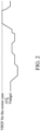
- FIG. 2 shows the waveforms of the reference voltage VREF and the target voltage Vtarget in accordance with an exemplary embodiment of the present invention.
- the reference voltage VREF satisfies the corner case of the target frequency FTAR that matches the load 120.
- the output voltage VOUT is adaptive to the status of the load 120.
- FIG. 3 shows waveforms to represent the response time of voltage regulation in accordance with an exemplary embodiment of the present invention.
- Waveform 302 corresponds to cases where the voltage regulation is based on controlling the frequency of the output voltage to approach the target frequency, and no voltage feedback is applied.
- Waveform 304 corresponds to the voltage regulator 100 of FIG. 1 . The transition response of the voltage regulator 100 is improved.
Landscapes
- Engineering & Computer Science (AREA)
- Power Engineering (AREA)
- Continuous-Control Power Sources That Use Transistors (AREA)
- Dc-Dc Converters (AREA)
Abstract
Description
- The present invention relates to voltage regulators.
- A voltage regulator may control power switches to convert an input voltage to an output voltage.
- How to design a voltage regulator taking power efficiency and response time into consideration is an important issue in this field.
- A voltage regulator with dynamic voltage and frequency tracking is shown.
- A voltage regulator in accordance with an exemplary embodiment of the preset invention has power switches converting an input voltage into an output voltage, a control loop, a voltage comparator, and a target voltage generator. The control loop is coupled to the power switches to control the power switches to perform voltage regulation. The voltage comparator compares the output voltage to the target voltage to generate a first control signal to control the control loop. The target voltage generator generates the target voltage for the voltage comparator based on the frequency difference between the target frequency and the critical-path-related frequency, wherein the critical-path-related frequency depends on the output voltage. The power efficiency and response time are improved.
- In an exemplary embodiment, when the critical-path-related frequency is lower than the target frequency, the target voltage generator increases the target voltage to increase the critical-path-related frequency. When the critical-path-related frequency is higher than the target frequency, the target voltage generator decreases the target voltage to decrease the critical-path-related frequency.
- In an exemplary embodiment, the voltage regulator further has a clock generator, which is powered by the output voltage to generate the critical-path-related frequency that depends on the output voltage.
- In an exemplary embodiment, the clock generator makes the critical-path-related frequency higher when the output voltage is higher.
- In an exemplary embodiment, the target voltage generator has a dynamic voltage scaler, which generates a reference voltage to be adjusted according to the frequency difference between the target frequency and the critical-path-related frequency, and thereby generates the target voltage.
- In an exemplary embodiment, the target voltage generator further has a phase frequency detector and a reference voltage adjusting circuit. The phase frequency detector receives the target frequency and the critical-path-related frequency to obtain the frequency difference between the target frequency and the critical-path-related frequency. The reference voltage adjusting circuit is controlled by the frequency difference obtained by the phase frequency detector. The reference voltage adjusting circuit generates a correction voltage for adjusting the reference voltage to the target voltage.
- In an exemplary embodiment, the phase frequency detector further generates a second control signal for the control loop based on the frequency difference between the target frequency and the critical-path-related frequency. The second control signal is passed to the control loop without passing through the reference voltage adjusting circuit or the voltage comparator.
- In an exemplary embodiment, the digital loop codes of the control loop are adjusted according to the second control signal that is passed to the control loop without passing through the reference voltage adjusting circuit or the voltage comparator.
- In an exemplary embodiment, the dynamic voltage scaler is controlled by a target decision module to make the reference voltage match the load driven by the voltage regulator.
- In an exemplary embodiment, when controlling the dynamic voltage scaler to make the reference voltage match the load, the target decision module further adjusts the gain that the reference voltage adjusting circuit provides to amplify the frequency difference between the target frequency and the critical-path-related frequency.
- In an exemplary embodiment, when controlling the dynamic voltage scaler to make the reference voltage match the load, the target decision module disables the gain that the reference voltage adjusting circuit provides to amplify the frequency difference between the target frequency and the critical-path-related frequency.
- In an exemplary embodiment, the target decision module controls the dynamic voltage scaler to make the reference voltage related to the target frequency.
- In an exemplary embodiment, the target decision module sets the target frequency to match the load driven by the voltage regulator.
- In an exemplary embodiment, the target decision module controls the dynamic voltage scaler to make the reference voltage cover a corner case of the target frequency that matches the load driven by the voltage regulator.
- A detailed description is given in the following embodiments with reference to the accompanying drawings.
- The present invention can be more fully understood by reading the subsequent detailed description and examples with references made to the accompanying drawings, wherein:
-
FIG. 1 depicts avoltage regulator 100 in accordance with an exemplary embodiment of the preset invention; -
FIG. 2 shows the waveforms of the reference voltage VREF and the target voltage Vtarget in accordance with an exemplary embodiment of the present invention; and -
FIG. 3 shows waveforms to represent the response time of voltage regulation in accordance with an exemplary embodiment of the present invention. - The following description is made for the purpose of illustrating the general principles of the invention and should not be taken in a limiting sense. The scope of the invention is best determined by reference to the appended claims.
-
FIG. 1 depicts avoltage regulator 100 in accordance with an exemplary embodiment of the preset invention. Thevoltage regulator 100 haspower switches 102 converting an input voltage VIN into an output voltage VOUT, acontrol loop 104, avoltage comparator 106, and atarget voltage generator 108. Thecontrol loop 104 is coupled to the power switches 102 to control the power switches 102 to perform voltage regulation. Thevoltage comparator 106 compares the output voltage VOUT to the target voltage Vtarget to generate a first control signal CS1 to control thecontrol loop 104. Thetarget voltage generator 108 generates the target voltage Vtarget for thevoltage comparator 106 based on the frequency difference between the target frequency FTAR and the critical-path-related frequency FCP, wherein the critical-path-related frequency FCP depends on the output voltage VOUT. In such a structure, the voltage feedback control performed through thevoltage comparator 106 further takes the frequency change into consideration. Thevoltage regulator 100 provides the better power efficiency and the shorter response time. - In an exemplary embodiment, when the critical-path-related frequency FCP is lower than the target frequency FTAR, the
target voltage generator 108 increases the target voltage Vtarget to increase the critical-path-related frequency FCP. When the critical-path-related frequency FCP is higher than the target frequency FTAR, thetarget voltage generator 108 decreases the target voltage Vtarget to decrease the critical-path-related frequency FCP. - The
voltage regulator 100 further has aclock generator 110, which is powered by the output voltage VOUT to generate the critical-path-related frequency FCP that depends on the output voltage VOUT. - In an exemplary embodiment, the
clock generator 110 makes the critical-path-related frequency FCP higher when the output voltage VOUT is higher. - The
target voltage generator 108 further has adynamic voltage scaler 112, which generates a reference voltage VREF to be adjusted according to the frequency difference between the target frequency FTAR and the critical-path-related frequency FCP. Thus, the reference voltage VREF is adjusted to the target voltage Vtarget. - The
target voltage generator 108 further has aphase frequency detector 114 and a referencevoltage adjusting circuit 116. Thephase frequency detector 114 receives the target frequency FTAR and the critical-path-related frequency FCP to obtain the frequency difference between the target frequency FTAR and the critical-path-related frequency FCP. The referencevoltage adjusting circuit 116 is controlled by the frequency difference obtained by thephase frequency detector 114. The referencevoltage adjusting circuit 116 generates a correction voltage ΔV for adjusting the reference voltage VREF to the target voltage Vtarget. - There is an optional path for controlling the
control loop 104 based on the between the target frequency FTAR and the critical-path-related frequency FCP. As shown, thephase frequency detector 114 further generates a second control signal CS2 for thecontrol loop 104 based on the frequency difference between the target frequency FTAR and the critical-path-related frequency FCP. The second control signal CS2 is passed to thecontrol loop 104 without passing through the referencevoltage adjusting circuit 116 or thevoltage comparator 106. - In an exemplary embodiment, the digital loop codes of the
control loop 104 are adjusted according to the second control signal CS2 that is passed to thecontrol loop 104 without passing through the referencevoltage adjusting circuit 116 or thevoltage comparator 106. - In an exemplary embodiment, the
dynamic voltage scaler 112 is controlled by atarget decision module 118 to make the reference voltage VREF match theload 120 driven by the voltage regulator 100 (driven by the output voltage VOUT or using an output clock signal FOUT). - In an exemplary embodiment, when controlling the
dynamic voltage scaler 112 to make the reference voltage VREF match theload 120, thetarget decision module 118 further adjusts the gain that the referencevoltage adjusting circuit 116 provides to amplify the frequency difference between the target frequency FTAR and the critical-path-related frequency FCP. - In an exemplary embodiment, when controlling the
dynamic voltage scaler 112 to make the reference voltage VREF match theload 120, thetarget decision module 118 disables the gain that the referencevoltage adjusting circuit 116 provides to amplify the frequency difference between the target frequency FTAR and the critical-path-related frequency FCP. The correction voltage ΔV may be zero to turn off the control based on the frequency difference between the target frequency FTAR and the critical-path-related frequency FCP. - In an exemplary embodiment, the
target decision module 118 controls thedynamic voltage scaler 112 to make the reference voltage VREF related to the target frequency FTAR. - In an exemplary embodiment, the
target decision module 118 sets the target frequency FTAR to match theload 120 driven by thevoltage regulator 100. - In an exemplary embodiment, the
target decision module 118 searches a look-up table 122 according to the target frequency FTAR to control thedynamic voltage scaler 112 according to the search result. - In an exemplary embodiment, the
target decision module 118 controls thedynamic voltage scaler 112 to make the reference voltage VREF cover a corner case of the target frequency FTAR that matches theload 120. - The
target decision module 118 and the look-up table 122 may be implemented by computing hardware. -
FIG. 2 shows the waveforms of the reference voltage VREF and the target voltage Vtarget in accordance with an exemplary embodiment of the present invention. The reference voltage VREF satisfies the corner case of the target frequency FTAR that matches theload 120. After being adjusted by the correction voltage ΔV that changes according to the frequency different between the target frequency FTAR and the critical-path-related frequency FCP, a more power efficient target voltage Vtarget is generated. The output voltage VOUT is adaptive to the status of theload 120. -
FIG. 3 shows waveforms to represent the response time of voltage regulation in accordance with an exemplary embodiment of the present invention.Waveform 302 corresponds to cases where the voltage regulation is based on controlling the frequency of the output voltage to approach the target frequency, and no voltage feedback is applied.Waveform 304 corresponds to thevoltage regulator 100 ofFIG. 1 . The transition response of thevoltage regulator 100 is improved. - While the invention has been described by way of example and in terms of the preferred embodiments, it should be understood that the invention is not limited to the disclosed embodiments. On the contrary, it is intended to cover various modifications and similar arrangements (as would be apparent to those skilled in the art). Therefore, the scope of the appended claims should be accorded the broadest interpretation so as to encompass all such modifications and similar arrangements.
Claims (15)
- A voltage regulator with dynamic voltage and frequency tracking, comprising:power switches for voltage regulation, converting an input voltage into an output voltage;a control loop, coupled to the power switches to control the power switches to perform voltage regulation;a voltage comparator, comparing the output voltage to a target voltage to generate a first control signal to control the control loop; anda target voltage generator, generating the target voltage for the voltage comparator based on a frequency difference between a target frequency and a critical-path-related frequency;wherein the critical-path-related frequency depends on the output voltage.
- The voltage regulator with dynamic voltage and frequency tracking as claimed in claim 1, wherein:when the critical-path-related frequency is lower than the target frequency, the target voltage generator increases the target voltage to increase the critical-path-related frequency; andwhen the critical-path-related frequency is higher than the target frequency, the target voltage generator decreases the target voltage to decrease the critical-path-related frequency.
- The voltage regulator with dynamic voltage and frequency tracking as claimed in claim 1 or 2, further comprising:
a clock generator, powered by the output voltage to generate the critical-path-related frequency that depends on the output voltage. - The voltage regulator with dynamic voltage and frequency tracking as claimed in claim 3, wherein:
the clock generator makes the critical-path-related frequency higher when the output voltage is higher. - The voltage regulator with dynamic voltage and frequency tracking as claimed in claim 4, wherein the target voltage generator comprises:
a dynamic voltage scaler, generating a reference voltage to be adjusted according to the frequency difference between the target frequency and the critical-path-related frequency and thereby to generate the target voltage. - The voltage regulator with dynamic voltage and frequency tracking as claimed in claim 5, wherein the target voltage generator further comprises:a phase frequency detector, receiving the target frequency and the critical-path-related frequency to obtain the frequency difference between the target frequency and the critical-path-related frequency; anda reference voltage adjusting circuit, controlled by the frequency difference obtained by the phase frequency detector to generate a correction voltage for adjusting the reference voltage to the target voltage.
- The voltage regulator with dynamic voltage and frequency tracking as claimed in claim 6, wherein:
the phase frequency detector further generates a second control signal for the control loop based on the frequency difference between the target frequency and the critical-path-related frequency, wherein the second control signal is passed to the control loop without passing through the reference voltage adjusting circuit or the voltage comparator. - The voltage regulator with dynamic voltage and frequency tracking as claimed in claim 7, wherein:
according to the second control signal that is passed to the control loop without passing through the reference voltage adjusting circuit or the voltage comparator, digital loop codes of the control loop are adjusted. - The voltage regulator with dynamic voltage and frequency tracking as claimed in any one of claims 6 to 8, wherein:
the dynamic voltage scaler is controlled by a target decision module to make the reference voltage match a load driven by the voltage regulator. - The voltage regulator with dynamic voltage and frequency tracking as claimed in claim 9, wherein:
when controlling the dynamic voltage scaler to make the reference voltage match the load, the target decision module further adjusts a gain that the reference voltage adjusting circuit provides to amplify the frequency difference between the target frequency and the critical-path-related frequency. - The voltage regulator with dynamic voltage and frequency tracking as claimed in claim 10, wherein:
when controlling the dynamic voltage scaler to make the reference voltage match the load, the target decision module disables the gain that the reference voltage adjusting circuit provides to amplify the frequency difference between the target frequency and the critical-path-related frequency. - The voltage regulator with dynamic voltage and frequency tracking as claimed in any one of claims 9 to 11, wherein:
the target decision module controls the dynamic voltage scaler to make the reference voltage related to the target frequency. - The voltage regulator with dynamic voltage and frequency tracking as claimed in claim 12, wherein:
the target decision module sets the target frequency to match the load driven by the voltage regulator. - The voltage regulator with dynamic voltage and frequency tracking as claimed in claim 13, wherein:
the target decision module searches a look-up table according to the target frequency to control the dynamic voltage scaler according to the search result. - The voltage regulator with dynamic voltage and frequency tracking as claimed in claim 13 or 14, wherein:
the target decision module controls the dynamic voltage scaler to make the reference voltage cover a corner case of the target frequency that matches the load driven by the voltage regulator.
Applications Claiming Priority (3)
| Application Number | Priority Date | Filing Date | Title |
|---|---|---|---|
| US202263300078P | 2022-01-17 | 2022-01-17 | |
| US202263343581P | 2022-05-19 | 2022-05-19 | |
| US18/057,311 US12301116B2 (en) | 2022-01-17 | 2022-11-21 | Voltage regulator with dynamic voltage and frequency tracking |
Publications (1)
| Publication Number | Publication Date |
|---|---|
| EP4213359A1 true EP4213359A1 (en) | 2023-07-19 |
Family
ID=84923148
Family Applications (1)
| Application Number | Title | Priority Date | Filing Date |
|---|---|---|---|
| EP23151130.4A Pending EP4213359A1 (en) | 2022-01-17 | 2023-01-11 | Voltage regulator with dynamic voltage and frequency tracking |
Country Status (3)
| Country | Link |
|---|---|
| US (1) | US12301116B2 (en) |
| EP (1) | EP4213359A1 (en) |
| TW (1) | TWI858508B (en) |
Citations (6)
| Publication number | Priority date | Publication date | Assignee | Title |
|---|---|---|---|---|
| JP2008289106A (en) * | 2007-05-21 | 2008-11-27 | Alpine Electronics Inc | Digital amplifier |
| WO2016145646A1 (en) * | 2015-03-19 | 2016-09-22 | Tridonic Gmbh & Co. Kg | Dimming method for led converter |
| US20170346406A1 (en) * | 2016-05-27 | 2017-11-30 | Apple Inc. | Gain adjustment circuit to enhance stability of multiple-output ac/dc converters |
| EP3435507A1 (en) * | 2017-07-26 | 2019-01-30 | Tdk-Lambda Ltd | A scalable structure for connection of power supply units |
| EP3713377A1 (en) * | 2017-11-14 | 2020-09-23 | Koito Manufacturing Co., Ltd. | Vehicle lamp, illumination circuit for same, current driver circuit |
| US20210028701A1 (en) * | 2019-01-04 | 2021-01-28 | Silanna Asia Pte Ltd | Constant On-Time Converter with Frequency Control |
Family Cites Families (4)
| Publication number | Priority date | Publication date | Assignee | Title |
|---|---|---|---|---|
| TWI273764B (en) | 2004-11-25 | 2007-02-11 | Beyond Innovation Tech Co Ltd | Fluorescent tube driver circuit system of pulse-width modulation control |
| US10033273B1 (en) * | 2017-01-05 | 2018-07-24 | Semiconductor Components Industries, Llc | System and method for controlling switching power supply |
| CN107834875B (en) | 2017-11-14 | 2020-10-09 | 西安矽力杰半导体技术有限公司 | Frequency control circuit, control method thereof and switch type converter |
| CN112994453B (en) * | 2019-12-18 | 2025-02-11 | 力智电子股份有限公司 | Time signal generating circuit of power converter and control method thereof |
-
2022
- 2022-11-21 US US18/057,311 patent/US12301116B2/en active Active
-
2023
- 2023-01-11 EP EP23151130.4A patent/EP4213359A1/en active Pending
- 2023-01-16 TW TW112101674A patent/TWI858508B/en active
Patent Citations (6)
| Publication number | Priority date | Publication date | Assignee | Title |
|---|---|---|---|---|
| JP2008289106A (en) * | 2007-05-21 | 2008-11-27 | Alpine Electronics Inc | Digital amplifier |
| WO2016145646A1 (en) * | 2015-03-19 | 2016-09-22 | Tridonic Gmbh & Co. Kg | Dimming method for led converter |
| US20170346406A1 (en) * | 2016-05-27 | 2017-11-30 | Apple Inc. | Gain adjustment circuit to enhance stability of multiple-output ac/dc converters |
| EP3435507A1 (en) * | 2017-07-26 | 2019-01-30 | Tdk-Lambda Ltd | A scalable structure for connection of power supply units |
| EP3713377A1 (en) * | 2017-11-14 | 2020-09-23 | Koito Manufacturing Co., Ltd. | Vehicle lamp, illumination circuit for same, current driver circuit |
| US20210028701A1 (en) * | 2019-01-04 | 2021-01-28 | Silanna Asia Pte Ltd | Constant On-Time Converter with Frequency Control |
Also Published As
| Publication number | Publication date |
|---|---|
| TWI858508B (en) | 2024-10-11 |
| US12301116B2 (en) | 2025-05-13 |
| US20230231482A1 (en) | 2023-07-20 |
| TW202331444A (en) | 2023-08-01 |
Similar Documents
| Publication | Publication Date | Title |
|---|---|---|
| US8253507B2 (en) | Fixed-frequency control circuit and method for pulse width modulation | |
| JP5679681B2 (en) | Oscillation circuit and switching power supply | |
| US20020060560A1 (en) | Switching regulator | |
| US8797088B2 (en) | Charge pump feedback control device and method using the same | |
| JP4252485B2 (en) | Switching regulator control circuit, switching regulator, and switching regulator control method | |
| US20060043955A1 (en) | PWM controller for a voltage regulator | |
| US7279870B2 (en) | DC-DC converter and method of controlling DC-DC converter | |
| US20130169252A1 (en) | Switching Regulator and Control Circuit and Control Method Thereof | |
| US11128218B2 (en) | Adaptive frequency adjusting system | |
| US20210296995A1 (en) | Control circuit and control method for switching regulator | |
| US20050007167A1 (en) | PWM switching regulator control circuit | |
| US9966849B1 (en) | Current mode voltage converter having fast transient response | |
| WO2001033310A1 (en) | Methods and apparatus to predictably change the output voltage of regulators | |
| US20110031951A1 (en) | Frequency modulation control of a buck-boost power converter | |
| US11316428B2 (en) | Time signal generating circuit of power converter and control method thereof | |
| US20140340059A1 (en) | Timing generator and timing signal generation method for power converter | |
| WO2005006528A1 (en) | Power supply having multi-vector error amplifier for power factor correction | |
| US7095288B2 (en) | Logic system with adaptive supply voltage control | |
| US20140191742A1 (en) | Voltage Regulator, and Control Circuit and Control Method Thereof | |
| JP3190914B2 (en) | Buck-boost DC / DC converter | |
| US6977830B2 (en) | Power supply apparatus | |
| US7508180B2 (en) | Switching regulator for fixing a frequency | |
| US11863071B2 (en) | Power converter having smooth transition control mechanism | |
| US9467044B2 (en) | Timing generator and timing signal generation method for power converter | |
| US12301116B2 (en) | Voltage regulator with dynamic voltage and frequency tracking |
Legal Events
| Date | Code | Title | Description |
|---|---|---|---|
| PUAI | Public reference made under article 153(3) epc to a published international application that has entered the european phase |
Free format text: ORIGINAL CODE: 0009012 |
|
| STAA | Information on the status of an ep patent application or granted ep patent |
Free format text: STATUS: THE APPLICATION HAS BEEN PUBLISHED |
|
| AK | Designated contracting states |
Kind code of ref document: A1 Designated state(s): AL AT BE BG CH CY CZ DE DK EE ES FI FR GB GR HR HU IE IS IT LI LT LU LV MC ME MK MT NL NO PL PT RO RS SE SI SK SM TR |
|
| STAA | Information on the status of an ep patent application or granted ep patent |
Free format text: STATUS: REQUEST FOR EXAMINATION WAS MADE |
|
| 17P | Request for examination filed |
Effective date: 20240119 |
|
| RBV | Designated contracting states (corrected) |
Designated state(s): AL AT BE BG CH CY CZ DE DK EE ES FI FR GB GR HR HU IE IS IT LI LT LU LV MC ME MK MT NL NO PL PT RO RS SE SI SK SM TR |
|
| STAA | Information on the status of an ep patent application or granted ep patent |
Free format text: STATUS: EXAMINATION IS IN PROGRESS |
|
| 17Q | First examination report despatched |
Effective date: 20250925 |