EP4213200A1 - Heat-dissipating structure - Google Patents
Heat-dissipating structure Download PDFInfo
- Publication number
- EP4213200A1 EP4213200A1 EP21866650.1A EP21866650A EP4213200A1 EP 4213200 A1 EP4213200 A1 EP 4213200A1 EP 21866650 A EP21866650 A EP 21866650A EP 4213200 A1 EP4213200 A1 EP 4213200A1
- Authority
- EP
- European Patent Office
- Prior art keywords
- heat
- resin layer
- board
- heat transfer
- conductive layer
- Prior art date
- Legal status (The legal status is an assumption and is not a legal conclusion. Google has not performed a legal analysis and makes no representation as to the accuracy of the status listed.)
- Granted
Links
Images


Classifications
-
- H—ELECTRICITY
- H05—ELECTRIC TECHNIQUES NOT OTHERWISE PROVIDED FOR
- H05K—PRINTED CIRCUITS; CASINGS OR CONSTRUCTIONAL DETAILS OF ELECTRIC APPARATUS; MANUFACTURE OF ASSEMBLAGES OF ELECTRICAL COMPONENTS
- H05K7/00—Constructional details common to different types of electric apparatus
- H05K7/20—Modifications to facilitate cooling, ventilating, or heating
- H05K7/2039—Modifications to facilitate cooling, ventilating, or heating characterised by the heat transfer by conduction from the heat generating element to a dissipating body
- H05K7/20509—Multiple-component heat spreaders; Multi-component heat-conducting support plates; Multi-component non-closed heat-conducting structures
-
- H—ELECTRICITY
- H05—ELECTRIC TECHNIQUES NOT OTHERWISE PROVIDED FOR
- H05K—PRINTED CIRCUITS; CASINGS OR CONSTRUCTIONAL DETAILS OF ELECTRIC APPARATUS; MANUFACTURE OF ASSEMBLAGES OF ELECTRICAL COMPONENTS
- H05K7/00—Constructional details common to different types of electric apparatus
- H05K7/20—Modifications to facilitate cooling, ventilating, or heating
- H05K7/2039—Modifications to facilitate cooling, ventilating, or heating characterised by the heat transfer by conduction from the heat generating element to a dissipating body
-
- H—ELECTRICITY
- H05—ELECTRIC TECHNIQUES NOT OTHERWISE PROVIDED FOR
- H05K—PRINTED CIRCUITS; CASINGS OR CONSTRUCTIONAL DETAILS OF ELECTRIC APPARATUS; MANUFACTURE OF ASSEMBLAGES OF ELECTRICAL COMPONENTS
- H05K7/00—Constructional details common to different types of electric apparatus
- H05K7/20—Modifications to facilitate cooling, ventilating, or heating
- H05K7/2039—Modifications to facilitate cooling, ventilating, or heating characterised by the heat transfer by conduction from the heat generating element to a dissipating body
- H05K7/20436—Inner thermal coupling elements in heat dissipating housings, e.g. protrusions or depressions integrally formed in the housing
- H05K7/20445—Inner thermal coupling elements in heat dissipating housings, e.g. protrusions or depressions integrally formed in the housing the coupling element being an additional piece, e.g. thermal standoff
- H05K7/20454—Inner thermal coupling elements in heat dissipating housings, e.g. protrusions or depressions integrally formed in the housing the coupling element being an additional piece, e.g. thermal standoff with a conformable or flexible structure compensating for irregularities, e.g. cushion bags, thermal paste
-
- H—ELECTRICITY
- H10—SEMICONDUCTOR DEVICES; ELECTRIC SOLID-STATE DEVICES NOT OTHERWISE PROVIDED FOR
- H10W—GENERIC PACKAGES, INTERCONNECTIONS, CONNECTORS OR OTHER CONSTRUCTIONAL DETAILS OF DEVICES COVERED BY CLASS H10
- H10W40/00—Arrangements for thermal protection or thermal control
- H10W40/10—Arrangements for heating
-
- H—ELECTRICITY
- H10—SEMICONDUCTOR DEVICES; ELECTRIC SOLID-STATE DEVICES NOT OTHERWISE PROVIDED FOR
- H10W—GENERIC PACKAGES, INTERCONNECTIONS, CONNECTORS OR OTHER CONSTRUCTIONAL DETAILS OF DEVICES COVERED BY CLASS H10
- H10W40/00—Arrangements for thermal protection or thermal control
- H10W40/20—Arrangements for cooling
- H10W40/22—Arrangements for cooling characterised by their shape, e.g. having conical or cylindrical projections
-
- H—ELECTRICITY
- H10—SEMICONDUCTOR DEVICES; ELECTRIC SOLID-STATE DEVICES NOT OTHERWISE PROVIDED FOR
- H10W—GENERIC PACKAGES, INTERCONNECTIONS, CONNECTORS OR OTHER CONSTRUCTIONAL DETAILS OF DEVICES COVERED BY CLASS H10
- H10W40/00—Arrangements for thermal protection or thermal control
- H10W40/20—Arrangements for cooling
- H10W40/22—Arrangements for cooling characterised by their shape, e.g. having conical or cylindrical projections
- H10W40/226—Arrangements for cooling characterised by their shape, e.g. having conical or cylindrical projections characterised by projecting parts, e.g. fins to increase surface area
- H10W40/228—Arrangements for cooling characterised by their shape, e.g. having conical or cylindrical projections characterised by projecting parts, e.g. fins to increase surface area the projecting parts being wire-shaped or pin-shaped
-
- H—ELECTRICITY
- H10—SEMICONDUCTOR DEVICES; ELECTRIC SOLID-STATE DEVICES NOT OTHERWISE PROVIDED FOR
- H10W—GENERIC PACKAGES, INTERCONNECTIONS, CONNECTORS OR OTHER CONSTRUCTIONAL DETAILS OF DEVICES COVERED BY CLASS H10
- H10W40/00—Arrangements for thermal protection or thermal control
- H10W40/20—Arrangements for cooling
- H10W40/25—Arrangements for cooling characterised by their materials
-
- H—ELECTRICITY
- H10—SEMICONDUCTOR DEVICES; ELECTRIC SOLID-STATE DEVICES NOT OTHERWISE PROVIDED FOR
- H10W—GENERIC PACKAGES, INTERCONNECTIONS, CONNECTORS OR OTHER CONSTRUCTIONAL DETAILS OF DEVICES COVERED BY CLASS H10
- H10W40/00—Arrangements for thermal protection or thermal control
- H10W40/20—Arrangements for cooling
- H10W40/25—Arrangements for cooling characterised by their materials
- H10W40/251—Organics
-
- H—ELECTRICITY
- H10—SEMICONDUCTOR DEVICES; ELECTRIC SOLID-STATE DEVICES NOT OTHERWISE PROVIDED FOR
- H10W—GENERIC PACKAGES, INTERCONNECTIONS, CONNECTORS OR OTHER CONSTRUCTIONAL DETAILS OF DEVICES COVERED BY CLASS H10
- H10W40/00—Arrangements for thermal protection or thermal control
- H10W40/20—Arrangements for cooling
- H10W40/25—Arrangements for cooling characterised by their materials
- H10W40/255—Arrangements for cooling characterised by their materials having a laminate or multilayered structure, e.g. direct bond copper [DBC] ceramic substrates
-
- H—ELECTRICITY
- H10—SEMICONDUCTOR DEVICES; ELECTRIC SOLID-STATE DEVICES NOT OTHERWISE PROVIDED FOR
- H10W—GENERIC PACKAGES, INTERCONNECTIONS, CONNECTORS OR OTHER CONSTRUCTIONAL DETAILS OF DEVICES COVERED BY CLASS H10
- H10W40/00—Arrangements for thermal protection or thermal control
- H10W40/20—Arrangements for cooling
- H10W40/25—Arrangements for cooling characterised by their materials
- H10W40/258—Metallic materials
Definitions
- the present disclosure relates to a heat-dissipating structure.
- Patent Document 1 discloses a heat-dissipating structure in which a heating element such as a semiconductor package and a heat dissipator such as a heat sink are brought into close contact with each other with interposition of a multilayer resin sheet and heat generated from the heating element is dissipated through the multilayer resin sheet.
- Patent Document 1 JP 2018-134779 A
- a void may be formed between the printed circuit board and the multilayer resin sheet.
- insulation properties between the printed circuit board and the multilayer resin sheet may be deteriorated.
- An object of the present disclosure is to provide a heat-dissipating structure having high insulation properties.
- a heat-dissipating structure configured to dispose between a heating element and a heat dissipation member, the heat dissipation being configured to dissipate heat generated by the heating element, the heat-dissipating structure including:
- the heat-dissipating structure includes at least one heat transfer portion including a plate-shaped heat transfer member and a conductive layer.
- the heat transfer member is provided between the board and the resin layer and extending along the board.
- the conductive layer is provided between the board and the resin layer and across the board and the heat transfer member, and partially disposed between the heat transfer member and the resin layer.
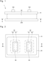
- a heat-dissipating structure 1 is configured to dispose between a heating element 100 and a heat dissipation member 200, the heat dissipation member being configured to dissipate heat generated by the heating element 100.
- the heating element 100 includes, for example, an electronic component such as a semiconductor, and the heat dissipation member 200 includes, for example, a heat sink.
- the heat-dissipating structure 1 includes a board 10, a resin layer 20 attached to the board 10, and a heat transfer portion provided between the board 10 and the resin layer 20.
- the heat transfer portion is configured to transfer heat generated by the heating element 100 to the heat dissipation member 200 through the resin layer 20.
- two heating elements 100 are attached to the board 10, and the heat-dissipating structure 1 includes two heat transfer portions (hereinafter, referred to as a first heat transfer portion 30 and a second heat transfer portion 40) corresponding to the respective heating elements 100.
- the board 10 is, for example, a printed circuit board including a copper foil and having a thickness of 50 ⁇ m or more, and includes a first surface 11 to which the heating element 100 is attached and a second surface 12 disposed on an opposite side from the first surface 11 in a thickness direction of the board as shown in FIG. 3 .
- the resin layer 20 is attached to the second surface 12.
- the resin layer 20 is made of, for example, silicone containing an inorganic filler, and has a thickness of 400 ⁇ m or more.
- the resin layer 20 includes a first end and a second end in a thickness direction of the resin layer, the first end being attached to the heating element 100 and the second end being attached to the heat dissipation member 200.
- the heat transfer portions 30, 40 include plate-shaped heat transfer members 31, 41 and conductive layers 32, 42, respectively.
- the heat transfer member 31, 41 is, for example, made of copper and formed by etching.
- the heat transfer member 31, 41 has, for example, a substantially rectangular film shape having a thickness of 5 ⁇ m or less, is provided between the board 10 and the resin layer 20, and extends along the second surface 12 of the board 10 as shown in FIG. 3 .
- the heat transfer member 31, 41 is connected to the heating elements 100 through the heat transfer layer 33, 43 extending through the board 10 in the thickness direction.
- the conductive layer 32, 42 is made of, for example, copper, silver, or graphite, and is formed by plating, sputtering, or lamination.
- the conductive layer 32, 42 has a thickness of 5 ⁇ m or less, and as shown in FIG. 3 , is provided between the board 10 and the resin layer 20 and across the board 10 and the heat transfer member 31, 41, and partially disposed between the heat transfer member 31, 41 and the resin layer 20.
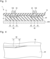
- the conductive layer 32, 42 is disposed to cover an entire peripheral edge of the heat transfer member 31, 41, and covers an entire void 50 formed by the board 10, the heat transfer member 31, and the resin layer 20 from the resin layer 20 side.
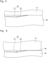
- the heat-dissipating structure 1 of the present embodiment influence of the thicknesses and elastic moduli of the conductive layer 32, 42 and the resin layer 20 on adhesion between the conductive layer 32, 42 and board 10 and between the resin layer 20 and board 10 was examined. Specifically, regarding a plurality of heat-dissipating structures 1 including the conductive layer 32, 42 having a thickness of 5 ⁇ m and an elastic modulus of 16 Gpa and the resin layer 20 having a different thickness and elastic modulus, in a state where the resin layer 20 was pressed toward the board 10 until the thickness thereof reached 70%, whether the conductive layer 32, 42 and resin layer 20 and the board 10 were in contact with each other or not was measured.
- FIG. 4 shows the heat-dissipating structure 1 when the ratio of the elastic modulus of the resin layer 20 to the elastic modulus of the conductive layer 32, 42 is 1/100,000, and the ratio of the thickness of the resin layer 20 to the thickness of the conductive layer 32, 42 is 160.
- the conductive layer 32, 42 and resin layer 20 and the board 10 were in contact with each other in many portions, and high adhesion was obtained.
- FIG. 5 shows the heat-dissipating structure 1 when a ratio of the elastic modulus of the resin layer 20 to the elastic modulus of the conductive layer 32, 42 is 1/100,000, and a ratio of the thickness of the resin layer 20 to the thickness of the conductive layer 32, 42 is 80.
- the conductive layer 32, 42 and resin layer 20 and the board 10 were in contact with each other in many portions, and high adhesion was obtained.
- FIG. 6 shows the heat-dissipating structure 1 when a ratio of the elastic modulus of the resin layer 20 to the elastic modulus of the conductive layer 32, 42 is 1/100,000, and a ratio of the thickness of the resin layer 20 to the thickness of the conductive layer 32, 42 is 40.
- the conductive layer 32, 42 and the board 10 were in contact with each other in many portions to secure sufficient adhesion, but a gap 60 was formed in many portions between the resin layer 20 and the board 10, and sufficiently high adhesion was not obtained.
- FIG. 7 shows the heat-dissipating structure 1 when a ratio of the elastic modulus of the resin layer 20 to the elastic modulus of the conductive layer 32, 42 is 1/10,000, and a ratio of the thickness of the resin layer 20 to the thickness of the conductive layer 32, 42 is 160.
- the conductive layer 32, 42 and resin layer 20 and the board 10 were in contact with each other in many portions, and high adhesion was obtained.
- FIG. 8 shows the heat-dissipating structure 1 when a ratio of the elastic modulus of the resin layer 20 to the elastic modulus of the conductive layer 32, 42 is 1/10,000, and a ratio of the thickness of the resin layer 20 to the thickness of the conductive layer 32, 42 is 80.
- the conductive layer 32, 42 and resin layer 20 and the board 10 were in contact with each other in many portions, and high adhesion was obtained.
- FIG. 9 shows the heat-dissipating structure 1 when a ratio of the elastic modulus of the resin layer 20 to the elastic modulus of the conductive layer 32, 42 is 1/10,000, and a ratio of the thickness of the resin layer 20 to the thickness of the conductive layer 32, 42 is 40.
- the conductive layer 32, 42 and the board 10 were in contact with each other in many portions to secure sufficient adhesion, but a gap 60 was formed in many portions between the resin layer 20 and the board 10, and high adhesion was not obtained.
- FIG. 10 shows the heat-dissipating structure 1 when a ratio of the elastic modulus of the resin layer 20 to the elastic modulus of the conductive layer 32, 42 is 1/1,000, and a ratio of the thickness of the resin layer 20 to the thickness of the conductive layer 32, 42 is 160.
- a gap 60 was formed in many portions between the resin layer 20 and the board 10, and a gap 70 was formed between the conductive layer 32, 42 and the board 10, and sufficiently high adhesion was not obtained.
- FIG. 11 shows the heat-dissipating structure 1 when a ratio of the elastic modulus of the resin layer 20 to the elastic modulus of the conductive layer 32, 42 is 1/1,000, and a ratio of the thickness of the resin layer 20 to the thickness of the conductive layer 32, 42 is 80.
- a gap 60 was formed in many portions between the resin layer 20 and the board 10, and a gap 70 was formed between the conductive layer 32, 42 and the board 10, and sufficiently high adhesion was not obtained.
- FIG. 12 shows the heat-dissipating structure 1 when a ratio of the elastic modulus of the resin layer 20 to the elastic modulus of the conductive layer 32, 42 is 1/1,000, and a ratio of the thickness of the resin layer 20 to the thickness of the conductive layer 32, 42 is 40.
- the conductive layer 32, 42 and the board 10 were in contact with each other in many portions to secure sufficient adhesion, but a gap 60 was formed in many portions between the resin layer 20 and the board 10, and high adhesion was not obtained.
- the heat-dissipating structure 1 includes a heat transfer portion 30 including: a plate-shaped heat transfer member 31, 41 and a conductive layer 32, 42.
- the heat transfer member 31, 41 is provided between the board 10 and the resin layer 20 and extending along the board 10.
- the conductive layer 32, 42 is provided between the board 10 and the resin layer 20 and across the board 10 and the heat transfer member 31, 41, the conductive layer 32, 42 being partially disposed between the heat transfer member 31, 41 and the resin layer 20.
- a ratio of the elastic modulus of the resin layer 20 to the elastic modulus of the conductive layer 32, 42 is 1/10,000 or less, and a ratio of the thickness of the resin layer 20 to the thickness of the conductive layer 32, 42 is 80 or more.
- adhesion of the conductive layer 32, 42 and the resin layer 20 to the board 10 can be enhanced.
- the heating element 100 is an electronic component, occurrence of partial discharge caused by the void 50 is suppressed, and a heat-dissipating structure 1 with high insulation properties can be achieved.
- the conductive layer 32, 42 is configured to cover the entire void 50, that is, to cover an entire peripheral edge of the heat transfer member 31, 41.
- the number of heat transfer portions may be one, or three or more.
- Each of the conductive layer 32, 42 and the resin layer 20 may be configured so that a ratio of the elastic modulus of the resin layer 20 to the elastic modulus of the conductive layer 32, 42 is larger than 1/10,000, or each of the conductive layer 32, 42 and the resin layer 20 may be configured so that a ratio of the thickness of the resin layer 20 to the thickness of the conductive layer 32, 42 is less than 80.
- the conductive layer 32, 42 is not limited to the case of being configured to cover the entire peripheral edge of the heat transfer member 31, 41, and may be configured to cover a part of the peripheral edge of the heat transfer member 31, 41 as shown in FIG. 13 .
- the conductive layer 32 of the first heat transfer portion 30 is disposed to cover a peripheral edge of the heat transfer member 31 of the first heat transfer portion 30 closest to the heat transfer member 41 of the second heat transfer portion 40 in the direction along the board 10.
- the heat-dissipating structure 1 can adopt any configuration capable of covering the void 50 with the conductive layer 32, 42.
- a heat-dissipating structure 1 is a heat-dissipating structure 1 configured to dispose between a heating element 100 and a heat dissipation member 200, the heat dissipation being configured to dissipate heat generated by the heating element 100, the heat-dissipating structure 1 including:
- a ratio of an elastic modulus of the resin layer 20 to an elastic modulus of the conductive layer 32, 42 is 1/10,000 or less, and a ratio of a thickness of the resin layer 20 to a thickness of the conductive layer 32, 42 is 80 or more.
- the conductive layer 32, 42 is configured to cover an entire peripheral edge of the heat transfer member 31, 41.
- the at least one heat transfer portion includes a first heat transfer portion 30 and a second heat transfer portion 40, and the conductive layer 32 of the first heat transfer portion 30 is disposed to cover a peripheral edge of the heat transfer member 31 of the first heat transfer portion 30 closest to the heat transfer member 41 of the second heat transfer portion 40 in a direction along the board 10.
- the heat-dissipating structure of the present disclosure can be applied to, for example, a power conditioner.
Landscapes
- Physics & Mathematics (AREA)
- Thermal Sciences (AREA)
- Engineering & Computer Science (AREA)
- Microelectronics & Electronic Packaging (AREA)
- Cooling Or The Like Of Semiconductors Or Solid State Devices (AREA)
- Cooling Or The Like Of Electrical Apparatus (AREA)
Abstract
Description
- The present disclosure relates to a heat-dissipating structure.
-
Patent Document 1 discloses a heat-dissipating structure in which a heating element such as a semiconductor package and a heat dissipator such as a heat sink are brought into close contact with each other with interposition of a multilayer resin sheet and heat generated from the heating element is dissipated through the multilayer resin sheet. - Patent Document 1:
JP 2018-134779 A - In the heat-dissipating structure, for example, when a multilayer resin sheet is attached to a plate surface of a printed circuit board having the plate surface provided with a plurality of patterns having large irregularities and different potentials, a void may be formed between the printed circuit board and the multilayer resin sheet. When such voids are formed, insulation properties between the printed circuit board and the multilayer resin sheet may be deteriorated.
- An object of the present disclosure is to provide a heat-dissipating structure having high insulation properties.
- A heat-dissipating structure according to an aspect of the present disclosure is a heat-dissipating structure configured to dispose between a heating element and a heat dissipation member, the heat dissipation being configured to dissipate heat generated by the heating element, the heat-dissipating structure including:
- a board configured to be attached to the heating element;
- a resin layer provided between the board and the heat dissipation member, the resin layer being attached to the board; and
- at least one heat transfer portion configured to transfer heat generated by the heating element to the heat dissipation member through the resin layer, wherein
- the at least one heat transfer portion includes:
- a heat transfer member, which is plate-shaped, provided between the board and the resin layer, the heat transfer member extending along the board, and
- a conductive layer provided between the board and the resin layer and across the board and the heat transfer member, the conductive layer being partially disposed between the heat transfer member and the resin layer.
- The heat-dissipating structure includes at least one heat transfer portion including a plate-shaped heat transfer member and a conductive layer. The heat transfer member is provided between the board and the resin layer and extending along the board. The conductive layer is provided between the board and the resin layer and across the board and the heat transfer member, and partially disposed between the heat transfer member and the resin layer. With this configuration, since the void formed by the board, the heat transfer member, and the resin layer can be covered with the conductive layer from the resin layer side, for example, when the heating element is an electronic component, occurrence of partial discharge caused by the void can be suppressed. As a result, a heat-dissipating structure having high insulation properties can be achieved.
-
-
FIG. 1 is a side view showing a heat-dissipating structure according to an embodiment of the present disclosure. -
FIG. 2 is a cross-sectional view taken along line II-II inFIG. 1 . -
FIG. 3 is a cross-sectional view taken along line III-III inFIG. 2 . -
FIG. 4 is a first view for illustrating the influence of the thicknesses and the elastic moduli of the conductive layer and the resin layer on the relationship with the adhesion between the conductive layer and resin layer and the board. -
FIG. 5 is a second view for illustrating the influence of the thicknesses and the elastic moduli of the conductive layer and the resin layer on the relationship with the adhesion between the conductive layer and resin layer and the board. -
FIG. 6 is a third view for illustrating the influence of the thicknesses and the elastic moduli of the conductive layer and the resin layer on the relationship with the adhesion between the conductive layer and resin layer and the board. -
FIG. 7 is a fourth view for illustrating the influence of the thicknesses and the elastic moduli of the conductive layer and the resin layer on the relationship with the adhesion between the conductive layer and resin layer and the board. -
FIG. 8 is a fifth view for illustrating the influence of the thicknesses and the elastic moduli of the conductive layer and the resin layer on the relationship with the adhesion between the conductive layer and resin layer and the board. -
FIG. 9 is a sixth view for illustrating the influence of the thicknesses and the elastic moduli of the conductive layer and the resin layer on the relationship with the adhesion between the conductive layer and resin layer and the board. -
FIG. 10 is a seventh view for illustrating the influence of the thicknesses and the elastic moduli of the conductive layer and the resin layer on the relationship with the adhesion between the conductive layer and resin layer and the board. -
FIG. 11 is an eighth view for illustrating the influence of the thicknesses and the elastic moduli of the conductive layer and the resin layer on the relationship with the adhesion between the conductive layer and resin layer and the board. -
FIG. 12 is a ninth view for illustrating the influence of the thicknesses and the elastic moduli of the conductive layer and the resin layer on the relationship with the adhesion between the conductive layer and resin layer and the board. -
FIG. 13 is a cross-sectional view showing a modification of the heat-dissipating structure inFIG. 1 . - Hereinafter, an example of the present disclosure will be described with reference to the accompanying drawings. It should be noted that in the following description, terms indicating specific directions or positions (for example, terms including "upper", "lower", "right", and "left") are used as necessary, but using these terms is to facilitate understanding of the present disclosure with reference to the drawings, and the technical scope of the present disclosure is not limited by the meaning of the terms. In addition, the following description is, essentially, merely illustrative and is not intended to limit the present disclosure, applied products thereof, or applications thereof. Furthermore, the drawings are schematic, and ratios and the like of the respective dimensions do not necessarily match those of actual ones.
- As shown in
FIG. 1 , a heat-dissipating structure 1 according to an embodiment of the present disclosure is configured to dispose between aheating element 100 and aheat dissipation member 200, the heat dissipation member being configured to dissipate heat generated by theheating element 100. Theheating element 100 includes, for example, an electronic component such as a semiconductor, and theheat dissipation member 200 includes, for example, a heat sink. - As shown in
FIGS. 1 to 3 , the heat-dissipating structure 1 includes aboard 10, aresin layer 20 attached to theboard 10, and a heat transfer portion provided between theboard 10 and theresin layer 20. The heat transfer portion is configured to transfer heat generated by theheating element 100 to theheat dissipation member 200 through theresin layer 20. In the present embodiment, twoheating elements 100 are attached to theboard 10, and the heat-dissipating structure 1 includes two heat transfer portions (hereinafter, referred to as a firstheat transfer portion 30 and a second heat transfer portion 40) corresponding to therespective heating elements 100. - The
board 10 is, for example, a printed circuit board including a copper foil and having a thickness of 50 µm or more, and includes afirst surface 11 to which theheating element 100 is attached and asecond surface 12 disposed on an opposite side from thefirst surface 11 in a thickness direction of the board as shown inFIG. 3 . Theresin layer 20 is attached to thesecond surface 12. - The
resin layer 20 is made of, for example, silicone containing an inorganic filler, and has a thickness of 400 µm or more. Theresin layer 20 includes a first end and a second end in a thickness direction of the resin layer, the first end being attached to theheating element 100 and the second end being attached to theheat dissipation member 200. - The
heat transfer portions heat transfer members conductive layers - The
heat transfer member heat transfer member board 10 and theresin layer 20, and extends along thesecond surface 12 of theboard 10 as shown inFIG. 3 . Theheat transfer member heating elements 100 through theheat transfer layer board 10 in the thickness direction. - The
conductive layer conductive layer FIG. 3 , is provided between theboard 10 and theresin layer 20 and across theboard 10 and theheat transfer member heat transfer member resin layer 20. As shown inFIG. 2 , theconductive layer heat transfer member entire void 50 formed by theboard 10, theheat transfer member 31, and theresin layer 20 from theresin layer 20 side. - Here, regarding the heat-
dissipating structure 1 of the present embodiment, influence of the thicknesses and elastic moduli of theconductive layer resin layer 20 on adhesion between theconductive layer board 10 and between theresin layer 20 andboard 10 was examined. Specifically, regarding a plurality of heat-dissipating structures 1 including theconductive layer resin layer 20 having a different thickness and elastic modulus, in a state where theresin layer 20 was pressed toward theboard 10 until the thickness thereof reached 70%, whether theconductive layer resin layer 20 and theboard 10 were in contact with each other or not was measured. -
FIG. 4 shows the heat-dissipating structure 1 when the ratio of the elastic modulus of theresin layer 20 to the elastic modulus of theconductive layer resin layer 20 to the thickness of theconductive layer dissipating structure 1 inFIG. 4 , theconductive layer resin layer 20 and theboard 10 were in contact with each other in many portions, and high adhesion was obtained. -
FIG. 5 shows the heat-dissipating structure 1 when a ratio of the elastic modulus of theresin layer 20 to the elastic modulus of theconductive layer resin layer 20 to the thickness of theconductive layer dissipating structure 1 inFIG. 5 , theconductive layer resin layer 20 and theboard 10 were in contact with each other in many portions, and high adhesion was obtained. -
FIG. 6 shows the heat-dissipatingstructure 1 when a ratio of the elastic modulus of theresin layer 20 to the elastic modulus of theconductive layer resin layer 20 to the thickness of theconductive layer structure 1 inFIG. 5 , theconductive layer board 10 were in contact with each other in many portions to secure sufficient adhesion, but agap 60 was formed in many portions between theresin layer 20 and theboard 10, and sufficiently high adhesion was not obtained. -
FIG. 7 shows the heat-dissipatingstructure 1 when a ratio of the elastic modulus of theresin layer 20 to the elastic modulus of theconductive layer resin layer 20 to the thickness of theconductive layer structure 1 inFIG. 7 , theconductive layer resin layer 20 and theboard 10 were in contact with each other in many portions, and high adhesion was obtained. -
FIG. 8 shows the heat-dissipatingstructure 1 when a ratio of the elastic modulus of theresin layer 20 to the elastic modulus of theconductive layer resin layer 20 to the thickness of theconductive layer structure 1 inFIG. 8 , theconductive layer resin layer 20 and theboard 10 were in contact with each other in many portions, and high adhesion was obtained. -
FIG. 9 shows the heat-dissipatingstructure 1 when a ratio of the elastic modulus of theresin layer 20 to the elastic modulus of theconductive layer resin layer 20 to the thickness of theconductive layer structure 1 inFIG. 9 , theconductive layer board 10 were in contact with each other in many portions to secure sufficient adhesion, but agap 60 was formed in many portions between theresin layer 20 and theboard 10, and high adhesion was not obtained. -
FIG. 10 shows the heat-dissipatingstructure 1 when a ratio of the elastic modulus of theresin layer 20 to the elastic modulus of theconductive layer resin layer 20 to the thickness of theconductive layer structure 1 inFIG. 10 , agap 60 was formed in many portions between theresin layer 20 and theboard 10, and agap 70 was formed between theconductive layer board 10, and sufficiently high adhesion was not obtained. -
FIG. 11 shows the heat-dissipatingstructure 1 when a ratio of the elastic modulus of theresin layer 20 to the elastic modulus of theconductive layer resin layer 20 to the thickness of theconductive layer structure 1 inFIG. 11 , agap 60 was formed in many portions between theresin layer 20 and theboard 10, and agap 70 was formed between theconductive layer board 10, and sufficiently high adhesion was not obtained. -
FIG. 12 shows the heat-dissipatingstructure 1 when a ratio of the elastic modulus of theresin layer 20 to the elastic modulus of theconductive layer resin layer 20 to the thickness of theconductive layer structure 1 inFIG. 12 , theconductive layer board 10 were in contact with each other in many portions to secure sufficient adhesion, but agap 60 was formed in many portions between theresin layer 20 and theboard 10, and high adhesion was not obtained. - From the above investigation results, it has been found that by configuring the heat-dissipating
structure 1 so that a ratio of the elastic modulus of theresin layer 20 to the elastic modulus of theconductive layer resin layer 20 to the thickness of theconductive layer conductive layer resin layer 20 to theboard 10 can be enhanced. - According to the heat-dissipating
structure 1, the following effects can be exerted. - The heat-dissipating
structure 1 includes aheat transfer portion 30 including: a plate-shapedheat transfer member conductive layer heat transfer member board 10 and theresin layer 20 and extending along theboard 10. Theconductive layer board 10 and theresin layer 20 and across theboard 10 and theheat transfer member conductive layer heat transfer member resin layer 20. With this configuration, since a void 50 formed by theboard 10, theheat transfer member resin layer 20 can be covered with theconductive layer resin layer 20 side, for example, when theheating element 100 is an electronic component, occurrence of partial discharge caused by the void 50 can be suppressed. As a result, a heat-dissipatingstructure 1 having high insulation properties can be achieved. - A ratio of the elastic modulus of the
resin layer 20 to the elastic modulus of theconductive layer resin layer 20 to the thickness of theconductive layer conductive layer resin layer 20 to theboard 10 can be enhanced. As a result, for example, when theheating element 100 is an electronic component, occurrence of partial discharge caused by the void 50 is suppressed, and a heat-dissipatingstructure 1 with high insulation properties can be achieved. - The
conductive layer entire void 50, that is, to cover an entire peripheral edge of theheat transfer member heating element 100 is an electronic component, occurrence of partial discharge caused by the void 50 can be more reliably suppressed. - According to the heat-dissipating
structure 1, following configuration can also be made. - The number of heat transfer portions may be one, or three or more.
- Each of the
conductive layer resin layer 20 may be configured so that a ratio of the elastic modulus of theresin layer 20 to the elastic modulus of theconductive layer conductive layer resin layer 20 may be configured so that a ratio of the thickness of theresin layer 20 to the thickness of theconductive layer - The
conductive layer heat transfer member heat transfer member FIG. 13 . In the heat-dissipatingstructure 1 inFIG. 13 , theconductive layer 32 of the firstheat transfer portion 30 is disposed to cover a peripheral edge of theheat transfer member 31 of the firstheat transfer portion 30 closest to theheat transfer member 41 of the secondheat transfer portion 40 in the direction along theboard 10. As described above, by disposing the respectiveconductive layers voids 51 closest to each other in the direction along theboard 10, occurrence of partial discharge caused by thevoids 50 can be more reliably suppressed. - That is, the heat-dissipating
structure 1 can adopt any configuration capable of covering the void 50 with theconductive layer - As described above, various embodiments in the present disclosure have been described in detail with reference to the drawings. Lastly, various aspects of the present disclosure will be described. It should be noted that in the following description, as an example, reference numerals are also added.
- A heat-dissipating
structure 1 according to a first aspect of the present disclosure is a heat-dissipatingstructure 1 configured to dispose between aheating element 100 and aheat dissipation member 200, the heat dissipation being configured to dissipate heat generated by theheating element 100, the heat-dissipatingstructure 1 including: - a
board 10 configured to be attached to theheating element 100; - a
resin layer 20 provided between theboard 10 and theheat dissipation member 200, theresin layer 20 being attached to theboard 10; and - at least one
heat transfer portion heating element 100 to theheat dissipation member 200 through theresin layer 20, wherein - the at least one
heat transfer portion - a
heat transfer member board 10 and theresin layer 20, theheat transfer member board 10, and - a
conductive layer board 10 and theresin layer 20 and across theboard 10 and theheat transfer member conductive layer heat transfer member resin layer 20.
- a
- In the heat-dissipating
structure 1 according to a second aspect of the present disclosure, a ratio of an elastic modulus of theresin layer 20 to an elastic modulus of theconductive layer resin layer 20 to a thickness of theconductive layer - In the heat-dissipating
structure 1 according to a third aspect of the present disclosure, theconductive layer heat transfer member - In the heat-dissipating
structure 1 according to a fourth aspect of the present disclosure, the at least one heat transfer portion includes a firstheat transfer portion 30 and a secondheat transfer portion 40, and
theconductive layer 32 of the firstheat transfer portion 30 is disposed to cover a peripheral edge of theheat transfer member 31 of the firstheat transfer portion 30 closest to theheat transfer member 41 of the secondheat transfer portion 40 in a direction along theboard 10. - Appropriately combining any embodiment or modification out of the various embodiments or modifications allows the effect of each of the embodiment or modification to be exhibited. In addition, a combination of embodiments, a combination of examples, or a combination of an embodiment and an example is possible, and a combination of features of different embodiments or examples is also possible.
- The present disclosure has been sufficiently described in connection with the preferred embodiments with reference to the accompanying drawings, and various modifications and corrections are apparent for those skilled in the art. It should be understood that as long as such modifications and corrections do not depart from the scope of the present disclosure by the attached claims, they are included therein.
- The heat-dissipating structure of the present disclosure can be applied to, for example, a power conditioner.
-
- 1
- heat-dissipating structure
- 10
- board
- 11
- first surface
- 12
- second surface
- 20
- resin layer
- 30, 40
- heat transfer portion
- 31, 41
- heat transfer member
- 32, 42
- conductive layer
- 33, 43
- heat transfer layer
- 50
- void
- 60, 70
- gap
- 100
- heating element
- 200
- heat dissipation member
Claims (4)
- A heat-dissipating structure configured to dispose between a heating element and a heat dissipation member, the heat dissipation being configured to dissipate heat generated by the heating element, the heat-dissipating structure comprising:a board configured to be attached to the heating element;a resin layer provided between the board and the heat dissipation member, the resin layer being attached to the board; andat least one heat transfer portion configured to transfer heat generated by the heating element to the heat dissipation member through the resin layer, whereinthe at least one heat transfer portion includes:a heat transfer member, which is plate-shaped, provided between the board and the resin layer, the heat transfer member extending along the board, anda conductive layer provided between the board and the resin layer and across the board and the heat transfer member, the conductive layer being partially disposed between the heat transfer member and the resin layer.
- The heat-dissipating structure according to claim 1, wherein
a ratio of an elastic modulus of the resin layer to an elastic modulus of the conductive layer is 1/10,000 or less, and a ratio of a thickness of the resin layer to a thickness of the conductive layer is 80 or more. - The heat-dissipating structure according to claim 1 or 2, wherein
the conductive layer is configured to cover an entire peripheral edge of the heat transfer member. - The heat-dissipating structure according to any one of claims 1 to 3, whereinthe at least one heat transfer portion includes a first heat transfer portion and a second heat transfer portion, andthe conductive layer of the first heat transfer portion is disposed to cover a peripheral edge of the heat transfer member of the first heat transfer portion closest to the heat transfer member of the second heat transfer portion in a direction along the board.
Applications Claiming Priority (2)
| Application Number | Priority Date | Filing Date | Title |
|---|---|---|---|
| JP2020153167A JP7574585B2 (en) | 2020-09-11 | 2020-09-11 | Heat dissipation structure |
| PCT/JP2021/032317 WO2022054691A1 (en) | 2020-09-11 | 2021-09-02 | Heat-dissipating structure |
Publications (3)
| Publication Number | Publication Date |
|---|---|
| EP4213200A1 true EP4213200A1 (en) | 2023-07-19 |
| EP4213200A4 EP4213200A4 (en) | 2024-10-09 |
| EP4213200B1 EP4213200B1 (en) | 2025-07-16 |
Family
ID=80632356
Family Applications (1)
| Application Number | Title | Priority Date | Filing Date |
|---|---|---|---|
| EP21866650.1A Active EP4213200B1 (en) | 2020-09-11 | 2021-09-02 | Heat-dissipating structure |
Country Status (5)
| Country | Link |
|---|---|
| US (1) | US12446193B2 (en) |
| EP (1) | EP4213200B1 (en) |
| JP (1) | JP7574585B2 (en) |
| CN (1) | CN116034636A (en) |
| WO (1) | WO2022054691A1 (en) |
Family Cites Families (11)
| Publication number | Priority date | Publication date | Assignee | Title |
|---|---|---|---|---|
| US7038310B1 (en) * | 1999-06-09 | 2006-05-02 | Matsushita Electric Industrial Co., Ltd. | Power module with improved heat dissipation |
| WO2008078788A1 (en) | 2006-12-26 | 2008-07-03 | Kyocera Corporation | Heat dissipating substrate and electronic device using the same |
| JP2009004731A (en) | 2007-01-29 | 2009-01-08 | Panasonic Corp | Insulating heat dissipation substrate, method for manufacturing the same, and circuit module using the same |
| JP2009260213A (en) * | 2008-03-24 | 2009-11-05 | Hitachi Chem Co Ltd | Method of manufacturing semiconductor device |
| JP5877056B2 (en) * | 2011-12-22 | 2016-03-02 | 日本シイエムケイ株式会社 | Insulated heat dissipation board for power module and manufacturing method thereof |
| JP6285638B2 (en) * | 2013-04-25 | 2018-02-28 | 日本メクトロン株式会社 | Printed wiring board and printed wiring board manufacturing method |
| JP7005906B2 (en) | 2017-02-21 | 2022-01-24 | 昭和電工マテリアルズ株式会社 | Multi-layer resin sheet, manufacturing method of multi-layer resin sheet, multi-layer resin sheet cured product, multi-layer resin sheet laminate, and multi-layer resin sheet laminate cured product |
| JP6390825B1 (en) * | 2017-03-01 | 2018-09-19 | 株式会社村田製作所 | Mounting board |
| JP6891075B2 (en) * | 2017-08-30 | 2021-06-18 | 株式会社 日立パワーデバイス | Power semiconductor module |
| US20200118906A1 (en) | 2018-10-16 | 2020-04-16 | Carbice Corporation | Gap fillers with independently tunable mechanical and thermal properties |
| JP7367309B2 (en) | 2019-02-08 | 2023-10-24 | 富士電機株式会社 | Semiconductor module, semiconductor device, and method for manufacturing semiconductor device |
-
2020
- 2020-09-11 JP JP2020153167A patent/JP7574585B2/en active Active
-
2021
- 2021-09-02 US US18/022,383 patent/US12446193B2/en active Active
- 2021-09-02 WO PCT/JP2021/032317 patent/WO2022054691A1/en not_active Ceased
- 2021-09-02 EP EP21866650.1A patent/EP4213200B1/en active Active
- 2021-09-02 CN CN202180056540.XA patent/CN116034636A/en active Pending
Also Published As
| Publication number | Publication date |
|---|---|
| JP2022047322A (en) | 2022-03-24 |
| CN116034636A (en) | 2023-04-28 |
| US12446193B2 (en) | 2025-10-14 |
| US20240040749A1 (en) | 2024-02-01 |
| WO2022054691A1 (en) | 2022-03-17 |
| EP4213200B1 (en) | 2025-07-16 |
| EP4213200A4 (en) | 2024-10-09 |
| JP7574585B2 (en) | 2024-10-29 |
Similar Documents
| Publication | Publication Date | Title |
|---|---|---|
| KR101015294B1 (en) | Heat dissipation plate and semiconductor device for semiconductor package | |
| US10504813B2 (en) | Heat sink assemblies for surface mounted devices | |
| CN106255308B (en) | Printed circuit board and electronic device | |
| KR20160045336A (en) | Emi shielding structure and thermal pad, and electronic circuit board assembly including the same | |
| CN105744721B (en) | Circuit substrate | |
| EP2717663B1 (en) | Radiator structure | |
| CN102017135A (en) | Substrate-mounted circuit module comprising components in a plurality of contact planes | |
| US20150351225A1 (en) | Metal-based mounting board and method of manufacturing metal-based mounting board | |
| JP6711098B2 (en) | Heat dissipation structure of semiconductor device | |
| GB2471497A (en) | Double sided multi-layer metal substrate PCB with SMD components mounted to top traces and lead wire components mounted to opposite side for heat dissipation | |
| CN113937080A (en) | Semiconductor module, power conversion device, and method for manufacturing semiconductor module | |
| KR20130123284A (en) | Thermal conductive sheet having self adhesive force | |
| EP2851945A1 (en) | Semiconductor module and semiconductor device | |
| EP4213200B1 (en) | Heat-dissipating structure | |
| JP2008205344A (en) | Thermally conductive substrate, manufacturing method thereof, and circuit module using the same | |
| JPH0685461B2 (en) | Metal core printed wiring board | |
| JP5087048B2 (en) | Circuit board with integrated heat dissipation components | |
| JP6381488B2 (en) | Circuit board | |
| JP2018006662A (en) | Circuit board and electric connection box | |
| WO2017115627A1 (en) | Inverter | |
| JP4992302B2 (en) | Power semiconductor module | |
| CN113903714A (en) | Semiconductor device with a plurality of semiconductor chips | |
| US20250365852A1 (en) | Backplate and method for protecting and cooling a printed circuit board | |
| CN115380374B (en) | Electrical assembly including heat dissipation layer | |
| JP7240953B2 (en) | metal base substrate |
Legal Events
| Date | Code | Title | Description |
|---|---|---|---|
| STAA | Information on the status of an ep patent application or granted ep patent |
Free format text: STATUS: THE INTERNATIONAL PUBLICATION HAS BEEN MADE |
|
| PUAI | Public reference made under article 153(3) epc to a published international application that has entered the european phase |
Free format text: ORIGINAL CODE: 0009012 |
|
| STAA | Information on the status of an ep patent application or granted ep patent |
Free format text: STATUS: REQUEST FOR EXAMINATION WAS MADE |
|
| 17P | Request for examination filed |
Effective date: 20230215 |
|
| AK | Designated contracting states |
Kind code of ref document: A1 Designated state(s): AL AT BE BG CH CY CZ DE DK EE ES FI FR GB GR HR HU IE IS IT LI LT LU LV MC MK MT NL NO PL PT RO RS SE SI SK SM TR |
|
| DAV | Request for validation of the european patent (deleted) | ||
| DAX | Request for extension of the european patent (deleted) | ||
| A4 | Supplementary search report drawn up and despatched |
Effective date: 20240906 |
|
| RIC1 | Information provided on ipc code assigned before grant |
Ipc: H01L 23/367 20060101ALN20240902BHEP Ipc: H01L 23/373 20060101ALN20240902BHEP Ipc: H05K 7/20 20060101ALI20240902BHEP Ipc: H01L 23/36 20060101AFI20240902BHEP |
|
| GRAP | Despatch of communication of intention to grant a patent |
Free format text: ORIGINAL CODE: EPIDOSNIGR1 |
|
| STAA | Information on the status of an ep patent application or granted ep patent |
Free format text: STATUS: GRANT OF PATENT IS INTENDED |
|
| RIC1 | Information provided on ipc code assigned before grant |
Ipc: H01L 23/367 20060101ALN20250317BHEP Ipc: H01L 23/373 20060101ALN20250317BHEP Ipc: H05K 7/20 20060101ALI20250317BHEP Ipc: H01L 23/36 20060101AFI20250317BHEP |
|
| INTG | Intention to grant announced |
Effective date: 20250328 |
|
| GRAS | Grant fee paid |
Free format text: ORIGINAL CODE: EPIDOSNIGR3 |
|
| GRAA | (expected) grant |
Free format text: ORIGINAL CODE: 0009210 |
|
| STAA | Information on the status of an ep patent application or granted ep patent |
Free format text: STATUS: THE PATENT HAS BEEN GRANTED |
|
| AK | Designated contracting states |
Kind code of ref document: B1 Designated state(s): AL AT BE BG CH CY CZ DE DK EE ES FI FR GB GR HR HU IE IS IT LI LT LU LV MC MK MT NL NO PL PT RO RS SE SI SK SM TR |
|
| REG | Reference to a national code |
Ref country code: GB Ref legal event code: FG4D |
|
| REG | Reference to a national code |
Ref country code: CH Ref legal event code: EP |
|
| REG | Reference to a national code |
Ref country code: DE Ref legal event code: R096 Ref document number: 602021034375 Country of ref document: DE |
|
| REG | Reference to a national code |
Ref country code: IE Ref legal event code: FG4D |
|
| PGFP | Annual fee paid to national office [announced via postgrant information from national office to epo] |
Ref country code: DE Payment date: 20250910 Year of fee payment: 5 |
|
| PGFP | Annual fee paid to national office [announced via postgrant information from national office to epo] |
Ref country code: AT Payment date: 20251020 Year of fee payment: 5 |
|
| REG | Reference to a national code |
Ref country code: NL Ref legal event code: MP Effective date: 20250716 |
|
| REG | Reference to a national code |
Ref country code: DE Ref legal event code: R079 Ref document number: 602021034375 Country of ref document: DE Free format text: PREVIOUS MAIN CLASS: H01L0023360000 Ipc: H10W0040200000 |
|
| PG25 | Lapsed in a contracting state [announced via postgrant information from national office to epo] |
Ref country code: PT Free format text: LAPSE BECAUSE OF FAILURE TO SUBMIT A TRANSLATION OF THE DESCRIPTION OR TO PAY THE FEE WITHIN THE PRESCRIBED TIME-LIMIT Effective date: 20251117 |
|
| PG25 | Lapsed in a contracting state [announced via postgrant information from national office to epo] |
Ref country code: NL Free format text: LAPSE BECAUSE OF FAILURE TO SUBMIT A TRANSLATION OF THE DESCRIPTION OR TO PAY THE FEE WITHIN THE PRESCRIBED TIME-LIMIT Effective date: 20250716 |
|
| REG | Reference to a national code |
Ref country code: AT Ref legal event code: MK05 Ref document number: 1814905 Country of ref document: AT Kind code of ref document: T Effective date: 20250716 |
|
| PG25 | Lapsed in a contracting state [announced via postgrant information from national office to epo] |
Ref country code: IS Free format text: LAPSE BECAUSE OF FAILURE TO SUBMIT A TRANSLATION OF THE DESCRIPTION OR TO PAY THE FEE WITHIN THE PRESCRIBED TIME-LIMIT Effective date: 20251116 |
|
| PG25 | Lapsed in a contracting state [announced via postgrant information from national office to epo] |
Ref country code: NO Free format text: LAPSE BECAUSE OF FAILURE TO SUBMIT A TRANSLATION OF THE DESCRIPTION OR TO PAY THE FEE WITHIN THE PRESCRIBED TIME-LIMIT Effective date: 20251016 |
|
| REG | Reference to a national code |
Ref country code: LT Ref legal event code: MG9D |
|
| PG25 | Lapsed in a contracting state [announced via postgrant information from national office to epo] |
Ref country code: AT Free format text: LAPSE BECAUSE OF FAILURE TO SUBMIT A TRANSLATION OF THE DESCRIPTION OR TO PAY THE FEE WITHIN THE PRESCRIBED TIME-LIMIT Effective date: 20250716 |
|
| PG25 | Lapsed in a contracting state [announced via postgrant information from national office to epo] |
Ref country code: FI Free format text: LAPSE BECAUSE OF FAILURE TO SUBMIT A TRANSLATION OF THE DESCRIPTION OR TO PAY THE FEE WITHIN THE PRESCRIBED TIME-LIMIT Effective date: 20250716 |
|
| PG25 | Lapsed in a contracting state [announced via postgrant information from national office to epo] |
Ref country code: HR Free format text: LAPSE BECAUSE OF FAILURE TO SUBMIT A TRANSLATION OF THE DESCRIPTION OR TO PAY THE FEE WITHIN THE PRESCRIBED TIME-LIMIT Effective date: 20250716 |
|
| PG25 | Lapsed in a contracting state [announced via postgrant information from national office to epo] |
Ref country code: GR Free format text: LAPSE BECAUSE OF FAILURE TO SUBMIT A TRANSLATION OF THE DESCRIPTION OR TO PAY THE FEE WITHIN THE PRESCRIBED TIME-LIMIT Effective date: 20251017 |
|
| PG25 | Lapsed in a contracting state [announced via postgrant information from national office to epo] |
Ref country code: SE Free format text: LAPSE BECAUSE OF FAILURE TO SUBMIT A TRANSLATION OF THE DESCRIPTION OR TO PAY THE FEE WITHIN THE PRESCRIBED TIME-LIMIT Effective date: 20250716 |
|
| PG25 | Lapsed in a contracting state [announced via postgrant information from national office to epo] |
Ref country code: LV Free format text: LAPSE BECAUSE OF FAILURE TO SUBMIT A TRANSLATION OF THE DESCRIPTION OR TO PAY THE FEE WITHIN THE PRESCRIBED TIME-LIMIT Effective date: 20250716 |
|
| PG25 | Lapsed in a contracting state [announced via postgrant information from national office to epo] |
Ref country code: PL Free format text: LAPSE BECAUSE OF FAILURE TO SUBMIT A TRANSLATION OF THE DESCRIPTION OR TO PAY THE FEE WITHIN THE PRESCRIBED TIME-LIMIT Effective date: 20250716 Ref country code: BG Free format text: LAPSE BECAUSE OF FAILURE TO SUBMIT A TRANSLATION OF THE DESCRIPTION OR TO PAY THE FEE WITHIN THE PRESCRIBED TIME-LIMIT Effective date: 20250716 |
|
| PG25 | Lapsed in a contracting state [announced via postgrant information from national office to epo] |
Ref country code: RS Free format text: LAPSE BECAUSE OF FAILURE TO SUBMIT A TRANSLATION OF THE DESCRIPTION OR TO PAY THE FEE WITHIN THE PRESCRIBED TIME-LIMIT Effective date: 20251016 |
|
| PG25 | Lapsed in a contracting state [announced via postgrant information from national office to epo] |
Ref country code: ES Free format text: LAPSE BECAUSE OF FAILURE TO SUBMIT A TRANSLATION OF THE DESCRIPTION OR TO PAY THE FEE WITHIN THE PRESCRIBED TIME-LIMIT Effective date: 20250716 |
|
| PG25 | Lapsed in a contracting state [announced via postgrant information from national office to epo] |
Ref country code: RO Free format text: LAPSE BECAUSE OF FAILURE TO SUBMIT A TRANSLATION OF THE DESCRIPTION OR TO PAY THE FEE WITHIN THE PRESCRIBED TIME-LIMIT Effective date: 20250716 |
|
| PG25 | Lapsed in a contracting state [announced via postgrant information from national office to epo] |
Ref country code: SM Free format text: LAPSE BECAUSE OF FAILURE TO SUBMIT A TRANSLATION OF THE DESCRIPTION OR TO PAY THE FEE WITHIN THE PRESCRIBED TIME-LIMIT Effective date: 20250716 |
|
| PG25 | Lapsed in a contracting state [announced via postgrant information from national office to epo] |
Ref country code: DK Free format text: LAPSE BECAUSE OF FAILURE TO SUBMIT A TRANSLATION OF THE DESCRIPTION OR TO PAY THE FEE WITHIN THE PRESCRIBED TIME-LIMIT Effective date: 20250716 |
|
| PG25 | Lapsed in a contracting state [announced via postgrant information from national office to epo] |
Ref country code: IT Free format text: LAPSE BECAUSE OF FAILURE TO SUBMIT A TRANSLATION OF THE DESCRIPTION OR TO PAY THE FEE WITHIN THE PRESCRIBED TIME-LIMIT Effective date: 20250716 |
|
| REG | Reference to a national code |
Ref country code: DE Ref legal event code: R097 Ref document number: 602021034375 Country of ref document: DE |
|
| PG25 | Lapsed in a contracting state [announced via postgrant information from national office to epo] |
Ref country code: CZ Free format text: LAPSE BECAUSE OF FAILURE TO SUBMIT A TRANSLATION OF THE DESCRIPTION OR TO PAY THE FEE WITHIN THE PRESCRIBED TIME-LIMIT Effective date: 20250716 |
|
| PG25 | Lapsed in a contracting state [announced via postgrant information from national office to epo] |
Ref country code: SK Free format text: LAPSE BECAUSE OF FAILURE TO SUBMIT A TRANSLATION OF THE DESCRIPTION OR TO PAY THE FEE WITHIN THE PRESCRIBED TIME-LIMIT Effective date: 20250716 Ref country code: EE Free format text: LAPSE BECAUSE OF FAILURE TO SUBMIT A TRANSLATION OF THE DESCRIPTION OR TO PAY THE FEE WITHIN THE PRESCRIBED TIME-LIMIT Effective date: 20250716 |
|
| REG | Reference to a national code |
Ref country code: CH Ref legal event code: H13 Free format text: ST27 STATUS EVENT CODE: U-0-0-H10-H13 (AS PROVIDED BY THE NATIONAL OFFICE) Effective date: 20260504 |
|
| PG25 | Lapsed in a contracting state [announced via postgrant information from national office to epo] |
Ref country code: LU Free format text: LAPSE BECAUSE OF NON-PAYMENT OF DUE FEES Effective date: 20250902 |
|
| PLBE | No opposition filed within time limit |
Free format text: ORIGINAL CODE: 0009261 |
|
| STAA | Information on the status of an ep patent application or granted ep patent |
Free format text: STATUS: NO OPPOSITION FILED WITHIN TIME LIMIT |
|
| REG | Reference to a national code |
Ref country code: CH Ref legal event code: L10 Free format text: ST27 STATUS EVENT CODE: U-0-0-L10-L00 (AS PROVIDED BY THE NATIONAL OFFICE) Effective date: 20260528 Ref country code: BE Ref legal event code: MM Effective date: 20250930 |
|
| 26N | No opposition filed |
Effective date: 20260417 |
|
| GBPC | Gb: european patent ceased through non-payment of renewal fee |
Effective date: 20251016 |
|
| PG25 | Lapsed in a contracting state [announced via postgrant information from national office to epo] |
Ref country code: LT Free format text: LAPSE BECAUSE OF FAILURE TO SUBMIT A TRANSLATION OF THE DESCRIPTION OR TO PAY THE FEE WITHIN THE PRESCRIBED TIME-LIMIT Effective date: 20250716 Ref country code: MC Free format text: LAPSE BECAUSE OF FAILURE TO SUBMIT A TRANSLATION OF THE DESCRIPTION OR TO PAY THE FEE WITHIN THE PRESCRIBED TIME-LIMIT Effective date: 20250716 |
|
| PG25 | Lapsed in a contracting state [announced via postgrant information from national office to epo] |
Ref country code: GB Free format text: LAPSE BECAUSE OF NON-PAYMENT OF DUE FEES Effective date: 20251016 |
|
| PG25 | Lapsed in a contracting state [announced via postgrant information from national office to epo] |
Ref country code: CH Free format text: LAPSE BECAUSE OF NON-PAYMENT OF DUE FEES Effective date: 20250930 Ref country code: BE Free format text: LAPSE BECAUSE OF NON-PAYMENT OF DUE FEES Effective date: 20250930 Ref country code: IE Free format text: LAPSE BECAUSE OF NON-PAYMENT OF DUE FEES Effective date: 20250902 |
|
| PG25 | Lapsed in a contracting state [announced via postgrant information from national office to epo] |
Ref country code: FR Free format text: LAPSE BECAUSE OF NON-PAYMENT OF DUE FEES Effective date: 20250916 |