EP4213137A1 - Display screen, electronic device, and method for manufacturing display screen - Google Patents
Display screen, electronic device, and method for manufacturing display screen Download PDFInfo
- Publication number
- EP4213137A1 EP4213137A1 EP22854449.0A EP22854449A EP4213137A1 EP 4213137 A1 EP4213137 A1 EP 4213137A1 EP 22854449 A EP22854449 A EP 22854449A EP 4213137 A1 EP4213137 A1 EP 4213137A1
- Authority
- EP
- European Patent Office
- Prior art keywords
- drive circuit
- display
- display area
- drive
- area
- Prior art date
- Legal status (The legal status is an assumption and is not a legal conclusion. Google has not performed a legal analysis and makes no representation as to the accuracy of the status listed.)
- Withdrawn
Links
Images




Classifications
-
- G—PHYSICS
- G09—EDUCATION; CRYPTOGRAPHY; DISPLAY; ADVERTISING; SEALS
- G09G—ARRANGEMENTS OR CIRCUITS FOR CONTROL OF INDICATING DEVICES USING STATIC MEANS TO PRESENT VARIABLE INFORMATION
- G09G3/00—Control arrangements or circuits, of interest only in connection with visual indicators other than cathode-ray tubes
- G09G3/03—Control arrangements or circuits, of interest only in connection with visual indicators other than cathode-ray tubes specially adapted for displays having non-planar surfaces, e.g. curved displays
-
- G—PHYSICS
- G09—EDUCATION; CRYPTOGRAPHY; DISPLAY; ADVERTISING; SEALS
- G09G—ARRANGEMENTS OR CIRCUITS FOR CONTROL OF INDICATING DEVICES USING STATIC MEANS TO PRESENT VARIABLE INFORMATION
- G09G3/00—Control arrangements or circuits, of interest only in connection with visual indicators other than cathode-ray tubes
- G09G3/20—Control arrangements or circuits, of interest only in connection with visual indicators other than cathode-ray tubes for presentation of an assembly of a number of characters, e.g. a page, by composing the assembly by combination of individual elements arranged in a matrix no fixed position being assigned to or needed to be assigned to the individual characters or partial characters
- G09G3/22—Control arrangements or circuits, of interest only in connection with visual indicators other than cathode-ray tubes for presentation of an assembly of a number of characters, e.g. a page, by composing the assembly by combination of individual elements arranged in a matrix no fixed position being assigned to or needed to be assigned to the individual characters or partial characters using controlled light sources
- G09G3/30—Control arrangements or circuits, of interest only in connection with visual indicators other than cathode-ray tubes for presentation of an assembly of a number of characters, e.g. a page, by composing the assembly by combination of individual elements arranged in a matrix no fixed position being assigned to or needed to be assigned to the individual characters or partial characters using controlled light sources using electroluminescent panels
- G09G3/32—Control arrangements or circuits, of interest only in connection with visual indicators other than cathode-ray tubes for presentation of an assembly of a number of characters, e.g. a page, by composing the assembly by combination of individual elements arranged in a matrix no fixed position being assigned to or needed to be assigned to the individual characters or partial characters using controlled light sources using electroluminescent panels semiconductive, e.g. using light-emitting diodes [LED]
- G09G3/3208—Control arrangements or circuits, of interest only in connection with visual indicators other than cathode-ray tubes for presentation of an assembly of a number of characters, e.g. a page, by composing the assembly by combination of individual elements arranged in a matrix no fixed position being assigned to or needed to be assigned to the individual characters or partial characters using controlled light sources using electroluminescent panels semiconductive, e.g. using light-emitting diodes [LED] organic, e.g. using organic light-emitting diodes [OLED]
- G09G3/3225—Control arrangements or circuits, of interest only in connection with visual indicators other than cathode-ray tubes for presentation of an assembly of a number of characters, e.g. a page, by composing the assembly by combination of individual elements arranged in a matrix no fixed position being assigned to or needed to be assigned to the individual characters or partial characters using controlled light sources using electroluminescent panels semiconductive, e.g. using light-emitting diodes [LED] organic, e.g. using organic light-emitting diodes [OLED] using an active matrix
- G09G3/3233—Control arrangements or circuits, of interest only in connection with visual indicators other than cathode-ray tubes for presentation of an assembly of a number of characters, e.g. a page, by composing the assembly by combination of individual elements arranged in a matrix no fixed position being assigned to or needed to be assigned to the individual characters or partial characters using controlled light sources using electroluminescent panels semiconductive, e.g. using light-emitting diodes [LED] organic, e.g. using organic light-emitting diodes [OLED] using an active matrix with pixel circuitry controlling the current through the light-emitting element
-
- G—PHYSICS
- G09—EDUCATION; CRYPTOGRAPHY; DISPLAY; ADVERTISING; SEALS
- G09G—ARRANGEMENTS OR CIRCUITS FOR CONTROL OF INDICATING DEVICES USING STATIC MEANS TO PRESENT VARIABLE INFORMATION
- G09G3/00—Control arrangements or circuits, of interest only in connection with visual indicators other than cathode-ray tubes
- G09G3/20—Control arrangements or circuits, of interest only in connection with visual indicators other than cathode-ray tubes for presentation of an assembly of a number of characters, e.g. a page, by composing the assembly by combination of individual elements arranged in a matrix no fixed position being assigned to or needed to be assigned to the individual characters or partial characters
- G09G3/22—Control arrangements or circuits, of interest only in connection with visual indicators other than cathode-ray tubes for presentation of an assembly of a number of characters, e.g. a page, by composing the assembly by combination of individual elements arranged in a matrix no fixed position being assigned to or needed to be assigned to the individual characters or partial characters using controlled light sources
- G09G3/30—Control arrangements or circuits, of interest only in connection with visual indicators other than cathode-ray tubes for presentation of an assembly of a number of characters, e.g. a page, by composing the assembly by combination of individual elements arranged in a matrix no fixed position being assigned to or needed to be assigned to the individual characters or partial characters using controlled light sources using electroluminescent panels
- G09G3/32—Control arrangements or circuits, of interest only in connection with visual indicators other than cathode-ray tubes for presentation of an assembly of a number of characters, e.g. a page, by composing the assembly by combination of individual elements arranged in a matrix no fixed position being assigned to or needed to be assigned to the individual characters or partial characters using controlled light sources using electroluminescent panels semiconductive, e.g. using light-emitting diodes [LED]
-
- G—PHYSICS
- G09—EDUCATION; CRYPTOGRAPHY; DISPLAY; ADVERTISING; SEALS
- G09G—ARRANGEMENTS OR CIRCUITS FOR CONTROL OF INDICATING DEVICES USING STATIC MEANS TO PRESENT VARIABLE INFORMATION
- G09G3/00—Control arrangements or circuits, of interest only in connection with visual indicators other than cathode-ray tubes
- G09G3/20—Control arrangements or circuits, of interest only in connection with visual indicators other than cathode-ray tubes for presentation of an assembly of a number of characters, e.g. a page, by composing the assembly by combination of individual elements arranged in a matrix no fixed position being assigned to or needed to be assigned to the individual characters or partial characters
- G09G3/34—Control arrangements or circuits, of interest only in connection with visual indicators other than cathode-ray tubes for presentation of an assembly of a number of characters, e.g. a page, by composing the assembly by combination of individual elements arranged in a matrix no fixed position being assigned to or needed to be assigned to the individual characters or partial characters by control of light from an independent source
- G09G3/36—Control arrangements or circuits, of interest only in connection with visual indicators other than cathode-ray tubes for presentation of an assembly of a number of characters, e.g. a page, by composing the assembly by combination of individual elements arranged in a matrix no fixed position being assigned to or needed to be assigned to the individual characters or partial characters by control of light from an independent source using liquid crystals
- G09G3/3611—Control of matrices with row and column drivers
- G09G3/3648—Control of matrices with row and column drivers using an active matrix
-
- G—PHYSICS
- G09—EDUCATION; CRYPTOGRAPHY; DISPLAY; ADVERTISING; SEALS
- G09G—ARRANGEMENTS OR CIRCUITS FOR CONTROL OF INDICATING DEVICES USING STATIC MEANS TO PRESENT VARIABLE INFORMATION
- G09G2300/00—Aspects of the constitution of display devices
- G09G2300/04—Structural and physical details of display devices
- G09G2300/0421—Structural details of the set of electrodes
- G09G2300/0426—Layout of electrodes and connections
-
- G—PHYSICS
- G09—EDUCATION; CRYPTOGRAPHY; DISPLAY; ADVERTISING; SEALS
- G09G—ARRANGEMENTS OR CIRCUITS FOR CONTROL OF INDICATING DEVICES USING STATIC MEANS TO PRESENT VARIABLE INFORMATION
- G09G2300/00—Aspects of the constitution of display devices
- G09G2300/08—Active matrix structure, i.e. with use of active elements, inclusive of non-linear two terminal elements, in the pixels together with light emitting or modulating elements
- G09G2300/0809—Several active elements per pixel in active matrix panels
- G09G2300/0814—Several active elements per pixel in active matrix panels used for selection purposes, e.g. logical AND for partial update
-
- G—PHYSICS
- G09—EDUCATION; CRYPTOGRAPHY; DISPLAY; ADVERTISING; SEALS
- G09G—ARRANGEMENTS OR CIRCUITS FOR CONTROL OF INDICATING DEVICES USING STATIC MEANS TO PRESENT VARIABLE INFORMATION
- G09G2300/00—Aspects of the constitution of display devices
- G09G2300/08—Active matrix structure, i.e. with use of active elements, inclusive of non-linear two terminal elements, in the pixels together with light emitting or modulating elements
- G09G2300/0809—Several active elements per pixel in active matrix panels
- G09G2300/0819—Several active elements per pixel in active matrix panels used for counteracting undesired variations, e.g. feedback or autozeroing
-
- G—PHYSICS
- G09—EDUCATION; CRYPTOGRAPHY; DISPLAY; ADVERTISING; SEALS
- G09G—ARRANGEMENTS OR CIRCUITS FOR CONTROL OF INDICATING DEVICES USING STATIC MEANS TO PRESENT VARIABLE INFORMATION
- G09G2300/00—Aspects of the constitution of display devices
- G09G2300/08—Active matrix structure, i.e. with use of active elements, inclusive of non-linear two terminal elements, in the pixels together with light emitting or modulating elements
- G09G2300/0809—Several active elements per pixel in active matrix panels
- G09G2300/0842—Several active elements per pixel in active matrix panels forming a memory circuit, e.g. a dynamic memory with one capacitor
- G09G2300/0861—Several active elements per pixel in active matrix panels forming a memory circuit, e.g. a dynamic memory with one capacitor with additional control of the display period without amending the charge stored in a pixel memory, e.g. by means of additional select electrodes
- G09G2300/0866—Several active elements per pixel in active matrix panels forming a memory circuit, e.g. a dynamic memory with one capacitor with additional control of the display period without amending the charge stored in a pixel memory, e.g. by means of additional select electrodes by means of changes in the pixel supply voltage
-
- G—PHYSICS
- G09—EDUCATION; CRYPTOGRAPHY; DISPLAY; ADVERTISING; SEALS
- G09G—ARRANGEMENTS OR CIRCUITS FOR CONTROL OF INDICATING DEVICES USING STATIC MEANS TO PRESENT VARIABLE INFORMATION
- G09G2310/00—Command of the display device
- G09G2310/02—Addressing, scanning or driving the display screen or processing steps related thereto
- G09G2310/0264—Details of driving circuits
-
- G—PHYSICS
- G09—EDUCATION; CRYPTOGRAPHY; DISPLAY; ADVERTISING; SEALS
- G09G—ARRANGEMENTS OR CIRCUITS FOR CONTROL OF INDICATING DEVICES USING STATIC MEANS TO PRESENT VARIABLE INFORMATION
- G09G2320/00—Control of display operating conditions
- G09G2320/02—Improving the quality of display appearance
- G09G2320/0233—Improving the luminance or brightness uniformity across the screen
-
- G—PHYSICS
- G09—EDUCATION; CRYPTOGRAPHY; DISPLAY; ADVERTISING; SEALS
- G09G—ARRANGEMENTS OR CIRCUITS FOR CONTROL OF INDICATING DEVICES USING STATIC MEANS TO PRESENT VARIABLE INFORMATION
- G09G2320/00—Control of display operating conditions
- G09G2320/02—Improving the quality of display appearance
- G09G2320/0242—Compensation of deficiencies in the appearance of colours
-
- G—PHYSICS
- G09—EDUCATION; CRYPTOGRAPHY; DISPLAY; ADVERTISING; SEALS
- G09G—ARRANGEMENTS OR CIRCUITS FOR CONTROL OF INDICATING DEVICES USING STATIC MEANS TO PRESENT VARIABLE INFORMATION
- G09G2320/00—Control of display operating conditions
- G09G2320/04—Maintaining the quality of display appearance
- G09G2320/043—Preventing or counteracting the effects of ageing
- G09G2320/045—Compensation of drifts in the characteristics of light emitting or modulating elements
Definitions
- This application relates to the field of electronic device technologies, and in particular, to a display, an electronic device, and a method for manufacturing a display.
- Embodiments of this application provide a display, and currents of drive circuits may be designed to be different to compensate for a display difference caused by different display conditions.
- an embodiment of this application provides a display.
- the display includes a first display area and a second display area that have an included angle, and further includes a first drive circuit and a second drive circuit.
- the first drive circuit provides a current for the first display area
- the second drive circuit provides a current for the second display area.
- Both the first drive circuit and the second drive circuit are provided with a drive transistor, and at least one structure parameter of the drive transistor of the first drive circuit and the drive transistor of the second drive circuit is different. In this way, the first drive circuit and the second drive circuit may provide different currents.
- an embodiment of this application further provides a first implementation of the first aspect.
- Structure parameters of the drive transistor include u, C ox , W, and L, where L is a channel length, W is a channel width, u is a carrier mobility, C ox is a gate capacitance per unit area, and a current provided by the drive circuit is positively correlated with uC ox W/L.
- L is a channel length
- W is a channel width
- u is a carrier mobility
- C ox is a gate capacitance per unit area
- a current provided by the drive circuit is positively correlated with uC ox W/L.
- a current of the drive circuit is positively correlated with uC ox W/L. Therefore, different currents can be obtained by adjusting at least one parameter of u, C ox , W, and L, and the design is simple.
- an embodiment of this application further provides a second implementation of the first aspect.
- Linear distances between two ends of channels of the drive transistor of the first drive circuit and the drive transistor of the second drive circuit are the same, but bending degrees or bending times of the channels are different to have different channel lengths. For example, a channel with more bending times is longer than a channel with fewer bending times. It can be learned that, by designing a bending degree and bending times of the drive transistor, a semiconductor channel length of the drive transistor can be changed, which makes the design of the semiconductor more flexible.
- an embodiment of this application further provides a third implementation of the first aspect.
- the drive transistor of the first drive circuit and the drive transistor of the second drive circuit have different grain sizes of semiconductor films to have different carrier mobility.
- a change of the grain size can be implemented by changing process parameters for processing, and therefore can be easily implemented.
- an embodiment of this application further provides a fourth implementation of the first aspect.
- a thickness of the first gate insulation layer of the drive transistor of the first drive circuit and a thickness of the first gate insulation layer of the drive transistor of the second drive circuit may be designed to be different. In this way, the drive transistor of the first drive circuit and the drive transistor of the second drive circuit may have different gate capacitance per unit area, and different currents may be provided, and such a design is also easy to process.
- an embodiment of this application further provides a fifth implementation of the first aspect.
- an embodiment of this application further provides a sixth implementation of the first aspect.
- the display is a curved screen, and the curved screen includes a curved display area and a main display area.
- the main display area is the first display area
- an area with any bending angle in the curved display area is the second display area.
- An area with any bending angle in the curved display area has an included angle with the main display area, and therefore, structure parameters of the drive transistors in each area with a bending angle and the main display area are designed to be different to obtain different currents.
- an embodiment of this application further provides a seventh implementation of the first aspect.
- included angles between areas with different bending angles and the main display area are different.
- a larger bending angle indicates a larger included angle between the area with a bending angle and the main display area, and a larger difference in viewing angle. Therefore, not only at least one structure parameter of the drive transistor of the second drive circuit corresponding to each area with a bending angle is different from that of the drive transistor corresponding to the main display area, but also a larger bending angle of the curved display area indicates a higher current provided by the corresponding second drive circuit after a structure parameter is adjusted, to compensate for a display difference caused by different included angles.
- an embodiment of this application further provides an eighth implementation of the first aspect.
- the main display area is corresponding to a plurality of first drive circuits, and structure parameters of drive transistors in the plurality of first drive circuits are the same.
- the main display area of the curved screen is set to a flat display area, the structure parameters of the drive transistors are the same, a same current may be provided, and a same component array can be set.
- an embodiment of this application further provides a ninth implementation of the first aspect.
- the display is an organic light-emitting display, a liquid crystal display, or a light-emitting diode display.
- a display uses a drive transistor, and a design of the transistor makes it easy to adjust a current.
- an embodiment of this application further provides an electronic device, including the display according to any one of the foregoing implementations, and the display has a same technical effect as the foregoing display.
- an embodiment of this application further provides a method for manufacturing a display, where the display includes a first display area and a second display area that have an included angle.
- a first drive circuit that provides a current for the first display area and a second drive circuit that provides a current for the second display area need to be processed.
- Both the first drive circuit and the second drive circuit are provided with a drive transistor, and the drive transistor controls a current of the first drive circuit or the second drive circuit.
- the drive transistor of the first drive circuit and the drive transistor of the second drive circuit are processed, at least one structure parameter of the two drive transistors is different to provide different currents, to compensate for a display difference caused by the included angle between the display areas.
- an embodiment of this application further provides a first implementation of the third aspect.
- Structure parameters of the drive transistor include u, C ox , W, and L, where L is a channel length, W is a channel width, u is a carrier mobility, C ox is a gate capacitance per unit area, and a current provided by the drive circuit is positively correlated with uC ox W/L.
- an embodiment of this application further provides a second implementation of the third aspect.
- Semiconductors of the drive transistor of the first drive circuit and the drive circuit of the second drive circuit may be processed by using an excimer laser annealing process, so that amorphous silicon is converted into polycrystalline silicon by using the process.
- Process parameters of the excimer laser annealing process includes a laser scanning time, laser energy, and a laser scanning quantity. Different process parameters affect parameters of the polycrystalline silicon, for example, a film grain size of the semiconductor. Therefore, when the drive transistor of the first drive circuit and the drive transistor of the second drive circuit are processed, the process parameters of the excimer laser annealing process may be adjusted, so that grain sizes of the semiconductor films of the drive transistor of the first drive circuit and the drive transistor of the second drive circuit are different.
- an embodiment of this application further provides a fourth implementation of the third aspect.
- the display is a curved screen, and the curved screen includes a curved display area and a main display area.
- the main display area is the first display area
- an area with any bending angle in the curved display area is the second display area.
- the first drive circuit and the second drive circuit are both designed in an array, and each area with a bending angle of the curved display area is corresponding to one column of second drive circuits.
- each column of the first drive circuits and the second drive circuits may be sequentially scanned, and when the drive transistor of the second drive circuit is scanned, at least one process parameter is adjusted, so that the grain sizes of the drive transistor films of each column of the second drive circuits are different from each other.
- Embodiments of this application provide a display of an electronic device, for example, a display of a mobile phone.
- the display includes a display layer and a drive circuit that provides a current for the display layer to drive the display layer to display.
- the display layer includes a plurality of pixel units, and each pixel unit is provided with a corresponding drive circuit.
- all drive circuits that drive the entire display layer to display adopt an array design with a same component structure, that is, drive circuits corresponding to any position in a display area of the display layer use a same component parameter.
- currents of the display at any position of the display area are the same.
- an organic light-emitting diode (organic light-emitting diode, OLED) display is used as an example for description.
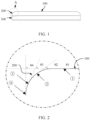
- FIG. 1 is a schematic diagram of a curved screen, that is, the display is a curved screen, and the curved screen includes a curved display area 200;
- FIG. 2 is an enlarged view of a part A in FIG. 1 ;
- FIG. 3 shows change of luminous brightness of a display with change of a viewing angle;
- FIG. 4 is a schematic diagram of display brightness attenuation and color cast of a curved screen.
- a display area of a display layer in a curved screen includes a curved display area 200 and a main display area 100 except the curved display area 200.
- the main display area 100 is a screen body area facing a user, and the curved display area 200 is located on two sides of the main display area 100.
- the curved display area 200 extends from an edge of the main display area 100 to a border 300 on two sides, and different positions of the curved display area 200 present different degrees of bending.
- the included angle is defined as a bending angle ⁇ , where larger bending angle ⁇ indicates a higher bending degree of the area.
- a viewing angle defined in this embodiment of this application is an angle between an observer's line of sight and a display area. Then, referring to FIG. 1 , when a user views the curved screen, a line of sight faces the main display area 100, that is, the viewing angle is 90 degrees, and the 90-degree viewing angle is a front viewing angle. In this case, an included angle between the line of sight of the user and the curved display area 200 on both sides is definitely greater than or less than 90 degrees. A larger bending angle ⁇ indicates a larger difference between a viewing angle of the user in this area and the front viewing angle.
- curved display area 200 included angles between areas with different bending angles ⁇ of the curved display area 200 and the line of sight of the user are different; and when the user's line of sight is facing the main display area 100, an area with a higher bending degree has a greater difference from the front viewing angle, lower display brightness, and more serious color cast.
- a structure parameter of the drive transistor in the drive circuit of the curved display area 200 is set to be different from that of the main display area 100, so that a drive circuit current of the curved display area 200 is different from a drive circuit current of the main display area 100, so as to compensate for a display brightness change or color cast that is subsequently caused by different viewing angles due to bending.
- FIG. 5 is a schematic diagram of a drive circuit of an OLED display.
- the drive transistor includes a plurality of transistors: T1, T2, T3, T4, T5, T6, and T7, where T1 operates in a saturation region, plays a drive role, is a drive transistor, and T2-T7 operate in a linear region, and play a switch role.
- FIG. 6 is a sectional view of the drive transistor T1 in FIG. 5 .
- the drive circuit shown in FIG. 5 is a drive circuit commonly used in an OLED display, and the drive circuit includes a source voltage VDD, a data voltage Data[m], a scanning signal SCAN[n], a scanning signal SCAN[n-1], an initialization voltage VI, a capacitor C1, a light-emitting signal Em[n], and a light-emitting diode OLED.
- each transistor in the drive circuit in FIG. 4 is a PMOS transistor
- corresponding transistors are enabled or disabled by controlling SCAN[n-1], SCAN[n], and Em[n] to change with time, which mainly includes the following several phases:
- FIG. 6 shows a cross section of a drive transistor T1 in a drive circuit.
- the drive transistor T1 includes a source (S electrode, Source) and a drain (D electrode, Drain) 12 that are on two ends, there is a semiconductor between the source 11 and the drain 12, and the semiconductor between the source 11 and the drain 12 is a channel 5.
- the semiconductor may be P-Si (Polysilicon), that is, polycrystalline silicon.
- the channel 5 is covered by a first gate insulation layer 4, a gate (Gate) 6 is disposed on the first gate insulation layer 4, and the gate 6 is covered by a second gate insulation layer 3; and an interlayer dielectric layer (ILD, Interlayer dielectric) is disposed on the second gate insulation layer 3.
- ILD Interlayer dielectric
- a length L of the channel 5 is a length of a semiconductor between the source 11 and the drain 12 of the drive transistor T1. From a perspective of FIG. 6 , a semiconductor size in a vertical direction to a semiconductor length is a width W of the channel 5 at a top viewing angle, and a vertical direction in FIG. 6 is a height direction of the channel 5.
- the foregoing formula is described by using a drive circuit shown in FIG. 5 as an example. When the drive circuit changes, 1/2(VDD-V data ) 2 in the current formula may change. For example, a value of 1/2 changes, or another parameter may be added to (V power -V data ), but regardless of how the drive circuit changes, the current I flowing through the OLED display is definitely positively correlated with uC ox W/L.
- a drive circuit that provides a current for the main display area 100 may be defined as a first drive circuit
- a drive circuit that provides a current for the curved display area 200 may be defined as a second drive circuit.
- both the main display area 100 and the curved display area 200 include a plurality of pixel units, and therefore, the main display area 100 and the curved display area 200 include a plurality of first drive circuits and a plurality of second drive circuits.
- structure parameters of a drive transistor of the second drive circuit may be adjusted, to increase a current of the curved display area 200, so as to improve brightness and eliminate color cast.
- the curved display area 200 includes areas with different bending angles ⁇ , and degrees of brightness attenuation and color cast are different. Therefore, current designs of areas with different bending angles ⁇ in the curved display area 200 are also different, that is, transistor structure parameter settings of the second drive circuit corresponding to areas with different bending angles ⁇ are also different. It can be learned that this adjustment manner can implement continuous adjustment of brightness and color cast of the display, and has a relatively large design and adjustment space.
- the current I in any bending angle ⁇ of the curved display area 200 is correlated with uC ox W/L. It may be learned that, in the second drive circuit corresponding to an area with any bending angle ⁇ , a change of any one of structure parameters u, C ox , W and L of the drive transistor of the second drive circuit may cause a change of magnitude of a current flowing through the area with the bending angle ⁇ , which leads to brightness attenuation and color cast in the area with the bending angle ⁇ caused by a change of a viewing angle.
- a change of any one of structure parameters u, C ox , W and L of the drive transistor of the second drive circuit may cause a change of magnitude of a current flowing through the area with the bending angle ⁇ , which leads to brightness attenuation and color cast in the area with the bending angle ⁇ caused
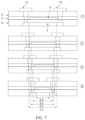
- FIG. 7 is a schematic diagram showing a comparison of lengths of a channel 5 at different positions in a curved display area 200 of a curved screen in Embodiment 1.
- FIG. 3 shows Four areas of the curved display area 200 .
- a second area 2and a third area 3 are successively areas with bending angles ⁇ 2 and ⁇ 3, and are located between the first area 1and the fourth area 4, where ⁇ 2 ⁇ 3.
- FIG. 7 shows channel length and width designs corresponding to the four areas in FIG. 3 .
- a current I of a drive circuit is positively correlated with uC ox W/L.
- u and C ox remain unchanged, if the ratio W/L of a width of the channel 5 to a length of the channel 5 of a drive transistor in the drive circuit changes, the supplied current also changes accordingly.
- drive transistors of second drive circuits in different areas of the curved display area 200 may be designed based on different bending angles ⁇ .
- FIG. 7 shows changes of the length L of the channel 5 in four different areas, which are respectively corresponding to the first area 1to the fourth area 4from top to bottom. The length of the channel 5 is gradually reduced, so that W/L is gradually increased, and a corresponding current is continuously increased.
- the length L of the channel 5 or the width W of the channel 5 in different areas may be separately changed.
- FIG. 7 shows that a length change of the channel 5 is separately changed.
- a width may also be separately changed, that is, the width of the channel 5 may be gradually increased from the first area 1to the fourth area 4.
- the length and the width of the channel 50 may also be changed at the same time.
- changes of the length and the width of the channel 50 cause a change of the ratio, and then cause a change of a current, so as to adapt to the change in the bending angle ⁇ of the curved display area 200, and finally compensate for the change of the display brightness and the color cast caused by the change of the viewing angle.
- FIG. 8 is a schematic diagram of a comparison of channel lengths and widths of areas with different bending angles ⁇ of a curved display area 200 of a curved screen in Embodiment 2.
- Four figures on the left are schematic diagrams of channel lengths of drive circuits corresponding to the four areas in FIG. 3
- figures on the right are corresponding schematic diagrams of channel widths.
- channels are respectively a channel 1a, a channel 1b, a channel 1c, and a channel 1d. Lengths of the channels are gradually decreased and widths are gradually increased. In this way, W/L is definitely gradually increased, and corresponding currents are continuously increased, so as to achieve the foregoing compensation purpose.
- the bending angle ⁇ gradually increases, if both the channel length and the width gradually increase or decrease, the purpose of increasing W/L can also be achieved.
- a specific increase or decrease range needs to be designed, so as to ensure that the W/L ratio changes as expected.
- Embodiment 1 and Embodiment 2 a change of the W/L ratio of the channel needs to be designed based on a change of the bending angle ⁇ of a corresponding area.
- Different display types may have different brightness changes or color cast problems in the curved display area 200 due to viewing angle changes, and design needs to be performed in combination with specific products to achieve the purpose of compensation.
- FIG. 9 is a schematic diagram of a shape change comparison of channels in different areas.
- FIG. 9 three figures in an upper part are schematic diagrams of a drive transistor channel of a first drive circuit in a main display area 100, and may be respectively defined as a first channel a, a second channel b, and a third channel c.
- Three figures in a lower part are schematic diagrams of drive transistor channels of drive circuits in the curved display area 200, and may be respectively defined as a fourth channel d, a fifth channel e, and a sixth channel f.
- a linear distance between two ends of the channel does not change. It may be learned that linear distances between two ends of channel a-f are the same. Only a bending degree of the channel and/or bending times of the channel are/is increased to increase a channel length.
- the channel length is a total path length that extends from one end of the channel to the other end.
- the first channel a has one bend, which is roughly Z-shaped
- the fourth channel d below the first channel a has two bends, which is roughly inverted ⁇ -shaped. In this case, a length of the fourth channel d is greater than a length of the first channel a.
- the second channel b in the middle is an inverted V-shaped structure
- the fifth channel e below the second channel b is an M-shaped structure, which is equivalent to increasing bending times.
- a length of the fifth channel e is greater than a length of the second channel b.
- the third channel c on the rightmost side is arc-shaped, and the sixth channel f below the third channel c continues to be concave in the middle of the arc shape, and a degree of bending is increased.
- a length of the sixth channel f is greater than a length of the third channel c.
- first channel a, second channel b, or third channel c in FIG. 9 may be used as channels that drive a drive transistor of the curved display area 200, and the longer fourth channel e, fifth channel f, or sixth channel g may be used as channels that drive a drive transistor of the main display area 100.
- the increase or decrease of the channel length and width is not limited to extension or shortening in corresponding length and width directions, but a change design of the length and width may be implemented by means of a shape change.
- a design of the drive transistor may be more flexible.
- the channel may be extended by increasing a quantity of bending times or increasing bending degrees. Therefore, channel layout may be performed based on a size condition of the drive transistor and location distribution of another circuit element.
- a shape change is not limited to changing a length of a channel. In FIG.
- a width of the fifth channel e decreases when a length increases compared with the second channel b
- a width of the sixth channel f decreases when a length increases compared with the third channel c, that is, a shape change may cause changes in both width and length.
- FIG. 10 is a schematic diagram showing a comparison of thicknesses of first gate insulation layers 4 of areas with different bending angles ⁇ in a curved display area 200 of a curved screen in Embodiment 3.
- a current I of a drive circuit is positively correlated with uC ox W/L.
- a change of the gate capacitance per unit area C ox with different bending angles ⁇ may also realize a change of the current.
- C ox ⁇ 0 ⁇ GI1 /d GI1
- ⁇ 0 is a vacuum permittivity
- ⁇ GI1 is a permittivity of the first gate insulation layer 4
- d GI1 is a thickness of the first gate insulation layer 4.
- C ox is inversely proportional to the thickness d GI1 of the first gate insulation layer 4. As shown in FIG.
- thicknesses of the first gate insulation layers 4 are respectively d1, d2, d3, and d4, and d1, d2, d3, and d4 gradually decrease as the bending angle ⁇ gradually increases, to ensure that the currents gradually increase, so that a current change meets a brightness and color cast change requirements, and display quality of each area is consistent. It may be learned that a change of another parameter in the gate capacitance per unit area C ox may also cause a change of a current, for example, the permittivity ⁇ GI1 of the first gate insulation layer 4 is changed. In this embodiment, a purpose of changing a current in a corresponding area can be achieved by changing only the thickness of the first gate insulation layer 4, and the design is simple.
- FIG. 11 is a schematic diagram showing a comparison of sizes of semiconductor film grains 5a of areas with different bending angles ⁇ in a curved display area 200 of a curved screen in Embodiment 4.
- a current I of a drive circuit is positively correlated with uC ox W/L.
- a carrier mobility u changes with different bending angles ⁇ , and when u and W/L remain unchanged, a current of a display area in an area with a bending angle ⁇ also correspondingly changes.
- a carrier mobility u of a semiconductor is affected by factors such as a size of a film grain of the semiconductor, doping density, and a defect status.
- FIG. 11 figures from left to right respectively correspond to semiconductor structures of drive transistors in drive circuits in the first area 1to the fourth area 4in FIG. 3 , and sizes of film grains of the semiconductors gradually increase.
- a larger semiconductor film grain 5a indicates a higher carrier mobility u.
- the size of the film grain 5a of the semiconductor of the drive transistor in the corresponding drive circuit can be controlled by a process, to control a semiconductor carrier mobility u in a corresponding area, so that a current of the corresponding area meets brightness and color cast change requirements, and display quality of each area is consistent.
- a length and a width of a channel may be changed separately or simultaneously.
- parameters u, C ox , W and L that affect the current they may be changed separately, or at least two parameters may be changed synchronously. This is not limited in this embodiment of this application, provided that a comprehensive result after the change adapts to the change of the bending angle ⁇ , so that the display effect of the corresponding area is consistent with that under the front viewing angle.
- FIG. 12 is a schematic diagram showing a comparative relationship between a current change and a display brightness change in areas with different bending angles ⁇ of a display.
- a straight line A is a first current curve, indicating that each area of the curved display area has a same current.
- a curve A' is a second current curve, indicating that currents provided by each area of the curved display area 200 gradually increase with increase of the curved angle ⁇ .
- a straight line B is a first display brightness curve, indicating that display brightness of each area of the curved display area 200 is consistent.
- a dashed line B' is a second display brightness curve, indicating that display brightness gradually decrease with increase of the curved angle ⁇ .
- a and B indicate an existing drive circuit arrangement solution.
- structure parameters of a drive transistor of a drive circuit are changed to adjust currents in areas with different bending angles ⁇ , and currents are supplied according to the curve A', so that display brightness of the curved display area 200 is consistent with that of the main display area 100, and is presented as the straight line B'.
- the curved display area shown in FIG. 2 is used as a schematic basis to lead to a difference in viewing angle, and then causes a problem of display brightness attenuation and color cast.
- the display in this embodiment of this application is not limited to the curved screen structure shown in FIG. 2 .
- a display includes display areas with different included angles, for example, a first display area and a second display area as defined, a difference in viewing angle is inevitable when a user simultaneously views the first display area and the second display area, and then a display of one display area has problems of display brightness attenuation and color cast compared with a display of the other display area.
- current magnitude of a corresponding position may be adjusted by changing structure parameters of a drive transistor of a drive circuit of a position where display brightness is attenuated and color cast is generated, to achieve a purpose of compensating for a difference in display effects.
- the main display area 100 is the first display area
- an area with any bending angle ⁇ in the curved display area 200 is the second display area.
- the display in this embodiment of this application is described by using an OLED screen as an example. It may be understood that the display may be another type of display, such as a liquid crystal display (liquid crystal display, LCD) or a light-emitting diode (light-emitting diode, LED) display.
- a liquid crystal display liquid crystal display, LCD
- a light-emitting diode light-emitting diode, LED
- the display is driven by a drive circuit, the current can be adjusted by changing the structure parameters of the drive transistor in the drive circuit.
- a display of a mobile phone is used as an example for description. It may be learned that a display may be disposed in another electronic device.
- the electronic device may alternatively be a mobile terminal such as a wearable device, an in-vehicle device, an augmented reality (augmented reality, AR)/virtual reality (virtual reality, VR) device, an ultra-mobile personal computer (ultra-mobile personal computer, UMPC), a netbook computer, or a personal digital assistant (personal digital assistant, PDA), or may be a professional photographing device such as a digital camera, a single-lens reflex camera/micro single camera, a motion camera, a cloud station camera, or a drone, provided that the electronic device is provided with a display. This is not specifically limited in this application.
- an embodiment of this application further provides a method for manufacturing a display, to process and manufacture the display according to any one of the foregoing embodiments.
- a channel that is, a semiconductor
- a thin film of amorphous silicon or polycrystalline silicon can be formed through chemical vapor deposition or physical vapor deposition.
- channels with different lengths or widths are obtained by changing shapes of deposition areas corresponding to drive transistors of a first drive circuit and a second drive circuit.
- the shape of the deposition area may be designed in advance as a whole, so that drive circuits with different structure parameters can be processed as a whole, and the processing is simple.
- a semiconductor of a drive transistor may be processed by using an excimer laser annealing process, and a semiconductor a-silicon (that is, amorphous silicon) formed by using the foregoing deposition process is processed into required polycrystalline silicon.
- laser scanning time, laser energy, and laser scanning times affect a size of a film grain of the semiconductor. For example, increasing laser energy and laser scanning time may increase a grain size.
- each bending angle of a curved display area 200 of the mobile phone corresponds to one row of drive circuits.
- a process parameter adjustment may be performed, and the operation is relatively simple.
Landscapes
- Engineering & Computer Science (AREA)
- Physics & Mathematics (AREA)
- Computer Hardware Design (AREA)
- General Physics & Mathematics (AREA)
- Theoretical Computer Science (AREA)
- Chemical & Material Sciences (AREA)
- Crystallography & Structural Chemistry (AREA)
- Devices For Indicating Variable Information By Combining Individual Elements (AREA)
- Electroluminescent Light Sources (AREA)
Abstract
Description
- This application claims priority to
Chinese Patent Application No. 202111447500.6, filed with the China National Intellectual Property Administration on November 30, 2021 - This application relates to the field of electronic device technologies, and in particular, to a display, an electronic device, and a method for manufacturing a display.
- Currently, a curved screen has emerged on a market, which brings an important breakthrough to an appearance of a product. A most intuitive feeling is that a non-display area at an edge is reduced, a screen ratio of a display area is increased, and appearance of a curved surface also puts forward a higher display requirement for a display. However, in a use process of an existing curved screen, display intensity attenuation and screen color cast may occur on both sides of the screen.
- Embodiments of this application provide a display, and currents of drive circuits may be designed to be different to compensate for a display difference caused by different display conditions.
- According to a first aspect, an embodiment of this application provides a display. The display includes a first display area and a second display area that have an included angle, and further includes a first drive circuit and a second drive circuit. The first drive circuit provides a current for the first display area, and the second drive circuit provides a current for the second display area. Both the first drive circuit and the second drive circuit are provided with a drive transistor, and at least one structure parameter of the drive transistor of the first drive circuit and the drive transistor of the second drive circuit is different. In this way, the first drive circuit and the second drive circuit may provide different currents. By changing structure parameters of drive transistors of drive circuits of different display areas that have an included angle, currents provided by the drive circuits may be changed, so that the display areas with different included angles have different currents, to compensate for a display brightness change or color cast caused by an included angle between the display areas, thereby ensuring that a display effect of an entire display area is consistent. It should be noted that this adjustment manner can implement continuous adjustment of brightness and color cast of the display, and has a large design and adjustment space. In addition, the display can be optimized and adjusted without increasing manufacturing costs or changing a main structure of the drive circuit.
- Based on the first aspect, an embodiment of this application further provides a first implementation of the first aspect.
- Structure parameters of the drive transistor include u, Cox, W, and L, where L is a channel length, W is a channel width, u is a carrier mobility, Cox is a gate capacitance per unit area, and a current provided by the drive circuit is positively correlated with uCoxW/L. According to a principle of the drive circuit, a current of the drive circuit is positively correlated with uCoxW/L. Therefore, different currents can be obtained by adjusting at least one parameter of u, Cox, W, and L, and the design is simple.
- Based on the first implementation of the first aspect, an embodiment of this application further provides a second implementation of the first aspect.
- Linear distances between two ends of channels of the drive transistor of the first drive circuit and the drive transistor of the second drive circuit are the same, but bending degrees or bending times of the channels are different to have different channel lengths. For example, a channel with more bending times is longer than a channel with fewer bending times. It can be learned that, by designing a bending degree and bending times of the drive transistor, a semiconductor channel length of the drive transistor can be changed, which makes the design of the semiconductor more flexible.
- Based on the first implementation of the first aspect, an embodiment of this application further provides a third implementation of the first aspect.
- The drive transistor of the first drive circuit and the drive transistor of the second drive circuit have different grain sizes of semiconductor films to have different carrier mobility. A change of the grain size can be implemented by changing process parameters for processing, and therefore can be easily implemented.
- Based on the first implementation of the first aspect, an embodiment of this application further provides a fourth implementation of the first aspect.
- The drive transistor includes a channel and a first gate insulation layer covering the channel, and a gate capacitance per unit area Cox=λε0εGI1/dGI1, where ε0 is a vacuum permittivity, εGI1 is a permittivity of the gate oxide layer, and dGI1 is a thickness of the first
gate insulation layer 4. A thickness of the first gate insulation layer of the drive transistor of the first drive circuit and a thickness of the first gate insulation layer of the drive transistor of the second drive circuit may be designed to be different. In this way, the drive transistor of the first drive circuit and the drive transistor of the second drive circuit may have different gate capacitance per unit area, and different currents may be provided, and such a design is also easy to process. - Based on the first aspect and the first to the fourth implementations of the first aspect, an embodiment of this application further provides a fifth implementation of the first aspect.
- Due to different angles between the first display area and the second display area, brightness attenuation or color cast may occur based on a difference in viewing angle. In a specific design, a current provided by a corresponding drive circuit of one of the first display area and the second display area that has lower display brightness may be greater than a current provided by the other drive circuit. In this way, the display area with lower brightness may obtain a higher current, to compensate for a difference in display brightness and eliminate color cast. The display area with lower display brightness herein refers to the display area with lower display brightness in a case in which the first display area and the second display area have a same drive circuit design. Based on the first aspect and the first to the fifth implementations of the first aspect, an embodiment of this application further provides a sixth implementation of the first aspect.
- The display is a curved screen, and the curved screen includes a curved display area and a main display area. The main display area is the first display area, and an area with any bending angle in the curved display area is the second display area. An area with any bending angle in the curved display area has an included angle with the main display area, and therefore, structure parameters of the drive transistors in each area with a bending angle and the main display area are designed to be different to obtain different currents.
- Based on the sixth implementation of the first aspect, an embodiment of this application further provides a seventh implementation of the first aspect.
- In the curved display area, included angles between areas with different bending angles and the main display area are different. A larger bending angle indicates a larger included angle between the area with a bending angle and the main display area, and a larger difference in viewing angle. Therefore, not only at least one structure parameter of the drive transistor of the second drive circuit corresponding to each area with a bending angle is different from that of the drive transistor corresponding to the main display area, but also a larger bending angle of the curved display area indicates a higher current provided by the corresponding second drive circuit after a structure parameter is adjusted, to compensate for a display difference caused by different included angles.
- Based on the sixth implementation of the first aspect, an embodiment of this application further provides an eighth implementation of the first aspect.
- The main display area is corresponding to a plurality of first drive circuits, and structure parameters of drive transistors in the plurality of first drive circuits are the same. The main display area of the curved screen is set to a flat display area, the structure parameters of the drive transistors are the same, a same current may be provided, and a same component array can be set.
- Based on the first aspect and the first to the eighth implementations of the first aspect, an embodiment of this application further provides a ninth implementation of the first aspect.
- The display is an organic light-emitting display, a liquid crystal display, or a light-emitting diode display. Such a display uses a drive transistor, and a design of the transistor makes it easy to adjust a current.
- According to a second aspect, an embodiment of this application further provides an electronic device, including the display according to any one of the foregoing implementations, and the display has a same technical effect as the foregoing display.
- According to a third aspect, an embodiment of this application further provides a method for manufacturing a display, where the display includes a first display area and a second display area that have an included angle. In this method, a first drive circuit that provides a current for the first display area and a second drive circuit that provides a current for the second display area need to be processed. Both the first drive circuit and the second drive circuit are provided with a drive transistor, and the drive transistor controls a current of the first drive circuit or the second drive circuit. When the drive transistor of the first drive circuit and the drive transistor of the second drive circuit are processed, at least one structure parameter of the two drive transistors is different to provide different currents, to compensate for a display difference caused by the included angle between the display areas.
- Based on the third aspect, an embodiment of this application further provides a first implementation of the third aspect.
- Structure parameters of the drive transistor include u, Cox, W, and L, where L is a channel length, W is a channel width, u is a carrier mobility, Cox is a gate capacitance per unit area, and a current provided by the drive circuit is positively correlated with uCoxW/L.
- Based on the third aspect, an embodiment of this application further provides a second implementation of the third aspect.
- Semiconductors of the drive transistor of the first drive circuit and the drive circuit of the second drive circuit may be processed by using an excimer laser annealing process, so that amorphous silicon is converted into polycrystalline silicon by using the process. Process parameters of the excimer laser annealing process includes a laser scanning time, laser energy, and a laser scanning quantity. Different process parameters affect parameters of the polycrystalline silicon, for example, a film grain size of the semiconductor. Therefore, when the drive transistor of the first drive circuit and the drive transistor of the second drive circuit are processed, the process parameters of the excimer laser annealing process may be adjusted, so that grain sizes of the semiconductor films of the drive transistor of the first drive circuit and the drive transistor of the second drive circuit are different.
- Based on the third aspect, an embodiment of this application further provides a fourth implementation of the third aspect.
- The display is a curved screen, and the curved screen includes a curved display area and a main display area. The main display area is the first display area, and an area with any bending angle in the curved display area is the second display area. The first drive circuit and the second drive circuit are both designed in an array, and each area with a bending angle of the curved display area is corresponding to one column of second drive circuits. During processing, each column of the first drive circuits and the second drive circuits may be sequentially scanned, and when the drive transistor of the second drive circuit is scanned, at least one process parameter is adjusted, so that the grain sizes of the drive transistor films of each column of the second drive circuits are different from each other.
-
-
FIG. 1 is a schematic diagram of a curved screen; -
FIG. 2 is an enlarged view of a part A inFIG. 1 ; -
FIG. 3 shows change of luminous brightness of a display with change of a viewing angle; -
FIG. 4 is a schematic diagram of display brightness attenuation and color cast of a curved screen; -
FIG. 5 is a schematic diagram of a drive circuit of an OLED display; -
FIG. 6 is a sectional view of a drive transistor T1 inFIG. 5 ; -
FIG. 7 is a schematic diagram showing a comparison of channel lengths at different positions in a curved display area of a curved screen inEmbodiment 1; -
FIG. 8 is a schematic diagram showing a comparison of channel lengths and widths at different positions in a curved display area of acurved screen Embodiment 2; -
FIG. 9 is a schematic diagram showing a comparison of channel shape changes at different positions; -
FIG. 10 is a schematic diagram showing a comparison of thicknesses of first gate insulation layers at different positions in a curved display area of a curved screen inEmbodiment 3; -
FIG. 11 is a schematic diagram showing a comparison of grain sizes of semiconductor films at different positions in a curved display area of a curved screen inEmbodiment 4; and -
FIG. 12 is a schematic diagram showing a comparative relationship between a current change and a display brightness change at different bending positions of a display. - Embodiments of this application provide a display of an electronic device, for example, a display of a mobile phone. The display includes a display layer and a drive circuit that provides a current for the display layer to drive the display layer to display. The display layer includes a plurality of pixel units, and each pixel unit is provided with a corresponding drive circuit. Currently, in a display, all drive circuits that drive the entire display layer to display adopt an array design with a same component structure, that is, drive circuits corresponding to any position in a display area of the display layer use a same component parameter. Correspondingly, currents of the display at any position of the display area are the same. In this embodiment of this application, an organic light-emitting diode (organic light-emitting diode, OLED) display is used as an example for description.
- Referring to
FIG. 1 to FIG. 4 ,FIG. 1 is a schematic diagram of a curved screen, that is, the display is a curved screen, and the curved screen includes acurved display area 200;FIG. 2 is an enlarged view of a part A inFIG. 1 ;FIG. 3 shows change of luminous brightness of a display with change of a viewing angle; andFIG. 4 is a schematic diagram of display brightness attenuation and color cast of a curved screen. - A display area of a display layer in a curved screen includes a
curved display area 200 and amain display area 100 except thecurved display area 200. Themain display area 100 is a screen body area facing a user, and thecurved display area 200 is located on two sides of themain display area 100. As shown inFIG. 4 , thecurved display area 200 extends from an edge of themain display area 100 to aborder 300 on two sides, and different positions of thecurved display area 200 present different degrees of bending. Based on a plane where themain display area 100 is located, different areas of thecurved display area 200 and the plane of themain display area 100 have different included angles, and the included angle is defined as a bending angle θ, where larger bending angle θ indicates a higher bending degree of the area. - A viewing angle defined in this embodiment of this application is an angle between an observer's line of sight and a display area. Then, referring to
FIG. 1 , when a user views the curved screen, a line of sight faces themain display area 100, that is, the viewing angle is 90 degrees, and the 90-degree viewing angle is a front viewing angle. In this case, an included angle between the line of sight of the user and thecurved display area 200 on both sides is definitely greater than or less than 90 degrees. A larger bending angle θ indicates a larger difference between a viewing angle of the user in this area and the front viewing angle. - Referring to
FIG. 3 again, when an angle between a line of sight and the display is 90 degrees, that is, in the front viewing angle, the display has maximum brightness. In another viewing angle, brightness of the display decreases to varying degrees as the viewing angle changes, and a larger deviation from the front viewing angle results in a greater display brightness decrease. It can be learned that, if component parameters of all areas of the entire display area of the curved screen are the same, referring toFIG. 3 ,because of a difference in a viewing angle, thecurved display area 200 on both sides definitely have brightness attenuation and color cast, that is, as shown inFIG. 4 . It may be understood that, in thecurved display area 200, included angles between areas with different bending angles θ of thecurved display area 200 and the line of sight of the user are different; and when the user's line of sight is facing themain display area 100, an area with a higher bending degree has a greater difference from the front viewing angle, lower display brightness, and more serious color cast. - Therefore, in this embodiment of this application, a structure parameter of the drive transistor in the drive circuit of the
curved display area 200 is set to be different from that of themain display area 100, so that a drive circuit current of thecurved display area 200 is different from a drive circuit current of themain display area 100, so as to compensate for a display brightness change or color cast that is subsequently caused by different viewing angles due to bending. - For a principle of adjusting the structure parameters of the drive transistor to change the current of the drive circuit, reference may be further made to
FIG. 5 and FIG. 6. FIG. 5 is a schematic diagram of a drive circuit of an OLED display. The drive transistor includes a plurality of transistors: T1, T2, T3, T4, T5, T6, and T7, where T1 operates in a saturation region, plays a drive role, is a drive transistor, and T2-T7 operate in a linear region, and play a switch role.FIG. 6 is a sectional view of the drive transistor T1 inFIG. 5 . - The drive circuit shown in
FIG. 5 is a drive circuit commonly used in an OLED display, and the drive circuit includes a source voltage VDD, a data voltage Data[m], a scanning signal SCAN[n], a scanning signal SCAN[n-1], an initialization voltage VI, a capacitor C1, a light-emitting signal Em[n], and a light-emitting diode OLED. In an example in which each transistor in the drive circuit inFIG. 4 is a PMOS transistor, corresponding transistors are enabled or disabled by controlling SCAN[n-1], SCAN[n], and Em[n] to change with time, which mainly includes the following several phases: - I. Initialization phase: The transistor T4 is enabled, and charge stored in the capacitor C1 flows into the VI through the transistor T4 to complete an initialization process.
- II. Anode reset compensation phase: The transistor T7 is enabled, OLED anode reset is completed, transistors T1, T2, and T3 are enabled, and data signal voltage is written into the capacitor C1 and maintained.
- III. Light-emitting phase: Transistors T5 and T6 are enabled, and a VDD voltage is driven. A current flows through a drive transistor T1 through an OLED component to complete light emitting. Because the data signal voltage in the second phase is written into the capacitor C1 and maintained, the voltage is also a gate voltage of the drive transistor T1, and the voltage is controlled by the Vdata[m].
- In this case, it can be obtained from a drive principle of the drive circuit that a current 1=1/2 uCox W/L(VDD-Vdata)2 that flows through the OLED display, where uCoxW/L is a structure parameter of the drive transistor T1, and specifically, VDD is a power signal, Vdata is a data voltage signal, u is a carrier mobility of the drive transistor T1, Cox is a gate capacitance per unit area of the drive transistor T1, W is a channel width of the drive transistor T1, and L is a channel length.
- A channel may be understood with reference to
FIG. 6. FIG. 6 shows a cross section of a drive transistor T1 in a drive circuit. The drive transistor T1 includes a source (S electrode, Source) and a drain (D electrode, Drain) 12 that are on two ends, there is a semiconductor between thesource 11 and thedrain 12, and the semiconductor between thesource 11 and thedrain 12 is achannel 5. The semiconductor may be P-Si (Polysilicon), that is, polycrystalline silicon. Thechannel 5 is covered by a firstgate insulation layer 4, a gate (Gate) 6 is disposed on the firstgate insulation layer 4, and thegate 6 is covered by a secondgate insulation layer 3; and an interlayer dielectric layer (ILD, Interlayer dielectric) is disposed on the secondgate insulation layer 3. In the foregoing formula, a length L of thechannel 5 is a length of a semiconductor between thesource 11 and thedrain 12 of the drive transistor T1. From a perspective ofFIG. 6 , a semiconductor size in a vertical direction to a semiconductor length is a width W of thechannel 5 at a top viewing angle, and a vertical direction inFIG. 6 is a height direction of thechannel 5. The foregoing formula is described by using a drive circuit shown inFIG. 5 as an example. When the drive circuit changes, 1/2(VDD-Vdata)2 in the current formula may change. For example, a value of 1/2 changes, or another parameter may be added to (Vpower-Vdata), but regardless of how the drive circuit changes, the current I flowing through the OLED display is definitely positively correlated with uCoxW/L. - In conclusion, in this embodiment of this application, to implement current adjustment, only a structure parameter of the drive transistor T1 in the drive circuit is adjusted. Provided that the structure parameter of the drive transistor in the drive circuit is changed, a current provided by the drive circuit to the display can be changed.
- For the curved screen, a drive circuit that provides a current for the
main display area 100 may be defined as a first drive circuit, and a drive circuit that provides a current for thecurved display area 200 may be defined as a second drive circuit. It should be understood that both themain display area 100 and thecurved display area 200 include a plurality of pixel units, and therefore, themain display area 100 and thecurved display area 200 include a plurality of first drive circuits and a plurality of second drive circuits. In this embodiment of this application, compared with the first drive circuit, structure parameters of a drive transistor of the second drive circuit may be adjusted, to increase a current of thecurved display area 200, so as to improve brightness and eliminate color cast. It can be learned that, in this embodiment of this application, display of the display can be optimized and adjusted without increasing manufacturing costs, changing a main structure of the drive circuit, or adjusting circuit control. Certainly, as described above, thecurved display area 200 includes areas with different bending angles θ, and degrees of brightness attenuation and color cast are different. Therefore, current designs of areas with different bending angles θ in thecurved display area 200 are also different, that is, transistor structure parameter settings of the second drive circuit corresponding to areas with different bending angles θ are also different. It can be learned that this adjustment manner can implement continuous adjustment of brightness and color cast of the display, and has a relatively large design and adjustment space. - As described above, the foregoing mentioned current flowing through the OLED display is 1=1/2 uCoxW/L(Vpower-Vdata)2, the current I in any bending angle θ of the
curved display area 200 is correlated with uCoxW/L. It may be learned that, in the second drive circuit corresponding to an area with any bending angle θ, a change of any one of structure parameters u, Cox, W and L of the drive transistor of the second drive circuit may cause a change of magnitude of a current flowing through the area with the bending angle θ, which leads to brightness attenuation and color cast in the area with the bending angle θ caused by a change of a viewing angle. For details, refer to the following embodiments. - As shown in
FIG. 7, FIG. 7 is a schematic diagram showing a comparison of lengths of achannel 5 at different positions in acurved display area 200 of a curved screen inEmbodiment 1. - This may be understood with reference to
FIG. 3 . Four areas of thecurved display area 200 are shown inFIG. 3 . A first area ①is an area where a bending angle θ1=0, and the area is a start of thecurved display area 200 and a boundary area between thecurved display area 200 and amain display area 100. A fourth area ④is an area where a bending angle θ4=90 degrees, and the area is an area with a maximum bending degree of thecurved display area 200. A second area ②and a third area ③are successively areas with bending angles θ2 and θ3, and are located between the first area ①and thefourth area ④, where θ2<θ3.FIG. 7 shows channel length and width designs corresponding to the four areas inFIG. 3 . - It can be learned from the foregoing principle description that a current I of a drive circuit is positively correlated with uCoxW/L. When u and Cox remain unchanged, if the ratio W/L of a width of the
channel 5 to a length of thechannel 5 of a drive transistor in the drive circuit changes, the supplied current also changes accordingly. In this embodiment, drive transistors of second drive circuits in different areas of thecurved display area 200 may be designed based on different bending angles θ.FIG. 7 shows changes of the length L of thechannel 5 in four different areas, which are respectively corresponding to the first area ①to the fourth area ④from top to bottom. The length of thechannel 5 is gradually reduced, so that W/L is gradually increased, and a corresponding current is continuously increased. It may be learned fromFIG. 3 that, from the first area ①to thefourth area ④ the bending angles θ gradually increase. If supplied currents are the same, display brightness gradually decreases, and color cast gradually becomes obvious. Currents in the first area ①to the fourtharea ④in Embodiment 1 gradually increase, which can compensate for a difference in viewing angle, so that display brightness of thecurved display area 200 and themain display area 100 with different bending angles θ can be consistent with themain display area 100. - It should be noted that a change of a W/L ratio will cause a change of a current. Therefore, the length L of the
channel 5 or the width W of thechannel 5 in different areas may be separately changed.FIG. 7 shows that a length change of thechannel 5 is separately changed. It may be understood that a width may also be separately changed, that is, the width of thechannel 5 may be gradually increased from the first area ①to thefourth area ④. Certainly, the length and the width of the channel 50 may also be changed at the same time. Provided that changes of the length and the width of the channel 50 cause a change of the ratio, and then cause a change of a current, so as to adapt to the change in the bending angle θ of thecurved display area 200, and finally compensate for the change of the display brightness and the color cast caused by the change of the viewing angle. - As shown in
FIG. 8, FIG. 8 is a schematic diagram of a comparison of channel lengths and widths of areas with different bending angles θ of acurved display area 200 of a curved screen inEmbodiment 2. Four figures on the left are schematic diagrams of channel lengths of drive circuits corresponding to the four areas inFIG. 3 , and figures on the right are corresponding schematic diagrams of channel widths. - In this embodiment, from a first area ①to a
fourth area ④, channels are respectively a channel 1a, a channel 1b, achannel 1c, and a channel 1d. Lengths of the channels are gradually decreased and widths are gradually increased. In this way, W/L is definitely gradually increased, and corresponding currents are continuously increased, so as to achieve the foregoing compensation purpose. Certainly, as the bending angle θ gradually increases, if both the channel length and the width gradually increase or decrease, the purpose of increasing W/L can also be achieved. However, in this case, a specific increase or decrease range needs to be designed, so as to ensure that the W/L ratio changes as expected. - It should be noted that, in
Embodiment 1 andEmbodiment 2, a change of the W/L ratio of the channel needs to be designed based on a change of the bending angle θ of a corresponding area. Different display types may have different brightness changes or color cast problems in thecurved display area 200 due to viewing angle changes, and design needs to be performed in combination with specific products to achieve the purpose of compensation. - In addition, referring to
FIG. 9, FIG. 9 is a schematic diagram of a shape change comparison of channels in different areas. - In
FIG. 9 , three figures in an upper part are schematic diagrams of a drive transistor channel of a first drive circuit in amain display area 100, and may be respectively defined as a first channel a, a second channel b, and a third channel c. Three figures in a lower part are schematic diagrams of drive transistor channels of drive circuits in thecurved display area 200, and may be respectively defined as a fourth channel d, a fifth channel e, and a sixth channel f. - In
FIG. 9 , specifically, when a channel length is increased, a linear distance between two ends of the channel does not change. It may be learned that linear distances between two ends of channel a-f are the same. Only a bending degree of the channel and/or bending times of the channel are/is increased to increase a channel length. The channel length is a total path length that extends from one end of the channel to the other end. InFIG. 9 , the first channel a has one bend, which is roughly Z-shaped, and the fourth channel d below the first channel a has two bends, which is roughly inverted Ω-shaped. In this case, a length of the fourth channel d is greater than a length of the first channel a. InFIG. 9 , the second channel b in the middle is an inverted V-shaped structure, and the fifth channel e below the second channel b is an M-shaped structure, which is equivalent to increasing bending times. In this case, a length of the fifth channel e is greater than a length of the second channel b. InFIG. 9 , the third channel c on the rightmost side is arc-shaped, and the sixth channel f below the third channel c continues to be concave in the middle of the arc shape, and a degree of bending is increased. In this case, a length of the sixth channel f is greater than a length of the third channel c. - It can be learned that the shorter first channel a, second channel b, or third channel c in
FIG. 9 may be used as channels that drive a drive transistor of thecurved display area 200, and the longer fourth channel e, fifth channel f, or sixth channel g may be used as channels that drive a drive transistor of themain display area 100. - It can be learned that the increase or decrease of the channel length and width is not limited to extension or shortening in corresponding length and width directions, but a change design of the length and width may be implemented by means of a shape change. In this way, a design of the drive transistor may be more flexible. For example, when a size of the drive transistor in a channel length direction is limited, the channel may be extended by increasing a quantity of bending times or increasing bending degrees. Therefore, channel layout may be performed based on a size condition of the drive transistor and location distribution of another circuit element. In addition, a shape change is not limited to changing a length of a channel. In
FIG. 10 , a width of the fifth channel e decreases when a length increases compared with the second channel b, and a width of the sixth channel f decreases when a length increases compared with the third channel c, that is, a shape change may cause changes in both width and length. - As shown in
FIG. 10, FIG. 10 is a schematic diagram showing a comparison of thicknesses of first gate insulation layers 4 of areas with different bending angles θ in acurved display area 200 of a curved screen inEmbodiment 3. - It can be learned from the foregoing principle description that a current I of a drive circuit is positively correlated with uCoxW/L. When u and W/L remain unchanged, a change of the gate capacitance per unit area Cox with different bending angles θ may also realize a change of the current. In a formula Cox=λε0εGI1/dGI1, ε0 is a vacuum permittivity, εGI1 is a permittivity of the first
gate insulation layer 4, and dGI1 is a thickness of the firstgate insulation layer 4. According to the formula, Cox is inversely proportional to the thickness dGI1 of the firstgate insulation layer 4. As shown inFIG. 10 , corresponding to the four areas with different bending angles θ1, θ2, θ3, and θ4 inFIG. 3 , thicknesses of the first gate insulation layers 4 are respectively d1, d2, d3, and d4, and d1, d2, d3, and d4 gradually decrease as the bending angle θ gradually increases, to ensure that the currents gradually increase, so that a current change meets a brightness and color cast change requirements, and display quality of each area is consistent. It may be learned that a change of another parameter in the gate capacitance per unit area Cox may also cause a change of a current, for example, the permittivity εGI1 of the firstgate insulation layer 4 is changed. In this embodiment, a purpose of changing a current in a corresponding area can be achieved by changing only the thickness of the firstgate insulation layer 4, and the design is simple. - As shown in
FIG. 11, FIG. 11 is a schematic diagram showing a comparison of sizes ofsemiconductor film grains 5a of areas with different bending angles θ in acurved display area 200 of a curved screen inEmbodiment 4. - It can be learned from the foregoing principle description that a current I of a drive circuit is positively correlated with uCoxW/L. A carrier mobility u changes with different bending angles θ, and when u and W/L remain unchanged, a current of a display area in an area with a bending angle θ also correspondingly changes. It can be learned from semiconductor knowledge that a carrier mobility u of a semiconductor is affected by factors such as a size of a film grain of the semiconductor, doping density, and a defect status. As shown in
FIG. 11 , figures from left to right respectively correspond to semiconductor structures of drive transistors in drive circuits in the first area ①to the fourth area ④inFIG. 3 , and sizes of film grains of the semiconductors gradually increase. A largersemiconductor film grain 5a indicates a higher carrier mobility u. In this case, the size of thefilm grain 5a of the semiconductor of the drive transistor in the corresponding drive circuit can be controlled by a process, to control a semiconductor carrier mobility u in a corresponding area, so that a current of the corresponding area meets brightness and color cast change requirements, and display quality of each area is consistent. - In the foregoing embodiment, a length and a width of a channel may be changed separately or simultaneously. Actually, for all parameters u, Cox, W and L that affect the current, they may be changed separately, or at least two parameters may be changed synchronously. This is not limited in this embodiment of this application, provided that a comprehensive result after the change adapts to the change of the bending angle θ, so that the display effect of the corresponding area is consistent with that under the front viewing angle.
- Referring to
FIG. 12, FIG. 12 is a schematic diagram showing a comparative relationship between a current change and a display brightness change in areas with different bending angles θ of a display. A straight line A is a first current curve, indicating that each area of the curved display area has a same current. A curve A' is a second current curve, indicating that currents provided by each area of thecurved display area 200 gradually increase with increase of the curved angle θ. A straight line B is a first display brightness curve, indicating that display brightness of each area of thecurved display area 200 is consistent. A dashed line B' is a second display brightness curve, indicating that display brightness gradually decrease with increase of the curved angle θ. - A and B indicate an existing drive circuit arrangement solution. In this embodiment of this application, structure parameters of a drive transistor of a drive circuit are changed to adjust currents in areas with different bending angles θ, and currents are supplied according to the curve A', so that display brightness of the
curved display area 200 is consistent with that of themain display area 100, and is presented as the straight line B'. - In addition, it may be understood that, in this embodiment of this application, the curved display area shown in
FIG. 2 is used as a schematic basis to lead to a difference in viewing angle, and then causes a problem of display brightness attenuation and color cast. However, the display in this embodiment of this application is not limited to the curved screen structure shown inFIG. 2 . Provided that a display includes display areas with different included angles, for example, a first display area and a second display area as defined, a difference in viewing angle is inevitable when a user simultaneously views the first display area and the second display area, and then a display of one display area has problems of display brightness attenuation and color cast compared with a display of the other display area. In this case, current magnitude of a corresponding position may be adjusted by changing structure parameters of a drive transistor of a drive circuit of a position where display brightness is attenuated and color cast is generated, to achieve a purpose of compensating for a difference in display effects. Actually, in the foregoing embodiment, themain display area 100 is the first display area, and an area with any bending angle θ in thecurved display area 200 is the second display area. - It should be noted that the display in this embodiment of this application is described by using an OLED screen as an example. It may be understood that the display may be another type of display, such as a liquid crystal display (liquid crystal display, LCD) or a light-emitting diode (light-emitting diode, LED) display. Provided that the display is driven by a drive circuit, the current can be adjusted by changing the structure parameters of the drive transistor in the drive circuit.
- In this embodiment of this application, a display of a mobile phone is used as an example for description. It may be learned that a display may be disposed in another electronic device. For example, the electronic device may alternatively be a mobile terminal such as a wearable device, an in-vehicle device, an augmented reality (augmented reality, AR)/virtual reality (virtual reality, VR) device, an ultra-mobile personal computer (ultra-mobile personal computer, UMPC), a netbook computer, or a personal digital assistant (personal digital assistant, PDA), or may be a professional photographing device such as a digital camera, a single-lens reflex camera/micro single camera, a motion camera, a cloud station camera, or a drone, provided that the electronic device is provided with a display. This is not specifically limited in this application.
- In addition, an embodiment of this application further provides a method for manufacturing a display, to process and manufacture the display according to any one of the foregoing embodiments. When a channel (that is, a semiconductor) of a drive transistor is processed, a thin film of amorphous silicon or polycrystalline silicon can be formed through chemical vapor deposition or physical vapor deposition. During deposition, channels with different lengths or widths are obtained by changing shapes of deposition areas corresponding to drive transistors of a first drive circuit and a second drive circuit. For a display, the shape of the deposition area may be designed in advance as a whole, so that drive circuits with different structure parameters can be processed as a whole, and the processing is simple.
- In addition, in an example in which semiconductors with different sizes of
film grains 5a need to be processed inEmbodiment 4, a semiconductor of a drive transistor may be processed by using an excimer laser annealing process, and a semiconductor a-silicon (that is, amorphous silicon) formed by using the foregoing deposition process is processed into required polycrystalline silicon. In this process, laser scanning time, laser energy, and laser scanning times affect a size of a film grain of the semiconductor. For example, increasing laser energy and laser scanning time may increase a grain size. When a semiconductor of a drive transistor of a first drive circuit and a drive transistor of a second drive circuit are manufactured, semiconductors with different sizes of film grains may be obtained by adjusting at least one of the foregoing parameters. In addition, as shown inFIG. 2 , for a mobile phone with a display, all drive circuit arrays are usually designed in an array. When semiconductors of drive transistors in each drive circuit are processed, laser scanning may be performed column by column. Therefore, for a mobile phone with a curved screen, each bending angle of acurved display area 200 of the mobile phone corresponds to one row of drive circuits. In this case, when laser scanning is performed on a row of drive circuits at each bending angle in thecurved display area 200, a process parameter adjustment may be performed, and the operation is relatively simple. - The principle and implementations of this application are described herein based on specific examples. The descriptions about the embodiments are merely intended to help understand the method and the core concept of this application. It should be noted that a person of ordinary skill in the art may make several improvements or modifications without departing from the principle of this application, and these improvements or modifications shall fall within the protection scope of this application.
Claims (15)
- A display, wherein the display comprises a first display area and a second display area that have an included angle, a first drive circuit provides a current for the first display area, a second drive circuit provides a current for the second display area, both the first drive circuit and the second drive circuit are provided with a drive transistor, and at least one structure parameter of the drive transistor of the first drive circuit and the drive transistor of the second drive circuit is different to provide different currents.
- The display according to claim 1, wherein the structure parameters comprise u, Cox, W, and L, wherein L is a channel length, W is a channel width, u is a carrier mobility, Cox is a gate capacitance per unit area, and a current provided by the drive circuit is positively correlated with uCoxW/L.
- The display according to claim 2, wherein a linear distance between two ends of a channel of the drive transistor of the first drive circuit and a linear distance between two ends of a channel of the drive transistor of the second drive circuit are the same, and the channels have different bending degrees or bending times to have different channel lengths.
- The display according to claim 2, wherein the drive transistor of the first drive circuit and the drive transistor of the second drive circuit have different grain sizes of semiconductor films to have different carrier mobility.
- The display according to claim 2, wherein the drive transistor comprises a channel and a first gate insulation layer covering the channel; and the drive transistor of the first drive circuit and the drive transistor of the second drive circuit have different thicknesses of first gate insulation layers to have different gate capacitance per unit area.
- The display according to any one of claims 1 to 5, wherein a current provided by a corresponding drive circuit of one of the first display area and the second display area that has lower display brightness may be greater than a current provided by the other drive circuit.
- The display according to any one of claims 1 to 6, wherein the display is a curved screen, the curved screen comprises a curved display area and a main display area, the main display area is the first display area, and an area with any bending angle in the curved display area is the second display area.
- The display according to claim 7, wherein in the curved display area, at least one structure parameter of the drive transistor of the second drive circuit corresponding to areas with different bending angles is different, and a larger bending angle indicates a higher current provided by the second drive circuit.
- The display according to claim 7, wherein a plurality of first drive circuits are corresponding to the main display area, and structure parameters of drive transistors in the plurality of first drive circuits are the same.
- The display according to any one of claims 1 to 9, wherein the display is an organic light-emitting display, a liquid crystal display, or a light-emitting diode display.
- An electronic device, comprising the display according to any one of claims 1 to 10.
- A method for manufacturing a display, wherein the display comprises a first display area and a second display area that have an included angle, a first drive circuit that provides a current for the first display area, and a second drive circuit that provides a current for the second display area; and both the first drive circuit and the second drive circuit are provided with a drive transistor, and when the drive transistor of the first drive circuit and the drive transistor of the second drive circuit are processed, at least one structure parameter of the drive transistor of the first drive circuit and the drive transistor of the second drive circuit is different to provide different currents.
- The method for manufacturing a display according to claim 12, wherein the structure parameters comprise u, Cox, W, and L, wherein L is a channel length, W is a channel width, u is a carrier mobility, Cox is a gate capacitance per unit area, and a current provided by the drive circuit is positively correlated with uCoxW/L.
- The method for manufacturing a display according to claim 13, wherein semiconductors of the drive transistor of the first drive circuit and the drive transistor of the second drive circuit are processed by using an excimer laser annealing process, and when the drive transistor of the first drive circuit and the drive transistor of the second drive circuit are processed, a process parameter is adjusted, so that grain sizes of semiconductor films of the drive transistor of the first drive circuit and the drive transistor of the second drive circuit are different; and the process parameters comprise: laser scanning time, laser energy, and laser scanning times.
- The method for manufacturing a display according to claim 14, wherein the display is a curved screen, the curved screen comprises a curved display area and a main display area, the main display area is the first display area, and an area with any bending angle in the curved display area is the second display area; and both the first drive circuit and the second drive circuit are designed in an array, and each area with a bending angle of the curved display area is corresponding to one column of second drive circuits; and
during processing, each column of the first drive circuits and the second drive circuits are sequentially scanned, and when the drive transistor of the second drive circuit is scanned, at least one of the process parameters is adjusted.
Applications Claiming Priority (2)
| Application Number | Priority Date | Filing Date | Title |
|---|---|---|---|
| CN202111447500.6A CN115064102A (en) | 2021-11-30 | 2021-11-30 | Display screen, electronic equipment and manufacturing method of display screen |
| PCT/CN2022/115062 WO2023098176A1 (en) | 2021-11-30 | 2022-08-26 | Display screen, electronic device, and method for manufacturing display screen |
Publications (1)
| Publication Number | Publication Date |
|---|---|
| EP4213137A1 true EP4213137A1 (en) | 2023-07-19 |
Family
ID=83196680
Family Applications (1)
| Application Number | Title | Priority Date | Filing Date |
|---|---|---|---|
| EP22854449.0A Withdrawn EP4213137A1 (en) | 2021-11-30 | 2022-08-26 | Display screen, electronic device, and method for manufacturing display screen |
Country Status (4)
| Country | Link |
|---|---|
| US (1) | US20240282260A1 (en) |
| EP (1) | EP4213137A1 (en) |
| CN (1) | CN115064102A (en) |
| WO (1) | WO2023098176A1 (en) |
Family Cites Families (16)
| Publication number | Priority date | Publication date | Assignee | Title |
|---|---|---|---|---|
| KR101950473B1 (en) * | 2012-10-05 | 2019-02-21 | 삼성디스플레이 주식회사 | Flexible display panel |
| KR102111407B1 (en) * | 2013-08-19 | 2020-05-15 | 엘지전자 주식회사 | Display apparatus and method for operating the same |
| KR20160061794A (en) * | 2014-11-24 | 2016-06-01 | 삼성전자주식회사 | Dispaly apparatus and controlling method thereof |
| CN106652902B (en) * | 2017-01-25 | 2019-01-22 | 上海天马有机发光显示技术有限公司 | Organic light-emitting display panel and driving method thereof, and organic light-emitting display device |
| KR102364165B1 (en) * | 2017-06-30 | 2022-02-16 | 엘지디스플레이 주식회사 | Display device and driving method of the same |
| CN107437400B (en) * | 2017-09-04 | 2020-08-07 | 上海天马有机发光显示技术有限公司 | Display panels and display devices |
| CN108305579B (en) * | 2018-01-26 | 2022-03-08 | 昆山国显光电有限公司 | Screen adjusting method and display device |
| KR102653121B1 (en) * | 2018-07-25 | 2024-04-02 | 삼성디스플레이 주식회사 | Organic light emitting diode display device |
| KR102792465B1 (en) * | 2018-11-15 | 2025-04-07 | 삼성디스플레이 주식회사 | Display device |
| CN109659347B (en) * | 2018-12-19 | 2021-02-26 | 武汉华星光电半导体显示技术有限公司 | Flexible OLED display panel and display device |
| CN110047914A (en) * | 2019-04-29 | 2019-07-23 | 厦门天马微电子有限公司 | Organic light emitting display panel and display device |
| CN110634932B (en) * | 2019-09-27 | 2022-08-16 | 京东方科技集团股份有限公司 | Design method of flexible display panel and flexible display panel |
| CN110648641B (en) * | 2019-09-27 | 2022-02-25 | 云谷(固安)科技有限公司 | A drive circuit for a display screen, a display screen and a display terminal |
| CN111430377B (en) * | 2020-04-10 | 2022-12-06 | 武汉华星光电半导体显示技术有限公司 | A display panel, its display method, and display device |
| CN111754873A (en) * | 2020-06-24 | 2020-10-09 | 武汉华星光电半导体显示技术有限公司 | Display panel and display device |
| CN113270078B (en) * | 2021-05-18 | 2022-09-23 | 昆山工研院新型平板显示技术中心有限公司 | Display panel, driving control method, device, equipment and storage medium thereof |
-
2021
- 2021-11-30 CN CN202111447500.6A patent/CN115064102A/en active Pending
-
2022
- 2022-08-26 US US18/024,560 patent/US20240282260A1/en not_active Abandoned
- 2022-08-26 EP EP22854449.0A patent/EP4213137A1/en not_active Withdrawn
- 2022-08-26 WO PCT/CN2022/115062 patent/WO2023098176A1/en not_active Ceased
Also Published As
| Publication number | Publication date |
|---|---|
| US20240282260A1 (en) | 2024-08-22 |
| CN115064102A (en) | 2022-09-16 |
| WO2023098176A1 (en) | 2023-06-08 |
Similar Documents
| Publication | Publication Date | Title |
|---|---|---|
| JP7558219B2 (en) | Light-emitting display device | |
| JP7671897B2 (en) | Semiconductor Device | |
| JP2025143301A (en) | display device | |
| US11764232B2 (en) | Display substrate, preparation method and driving method therefor, and display apparatus | |
| US8686426B2 (en) | Thin film transistor having plural semiconductive oxides, thin film transistor array panel and display device including the same, and manufacturing method of thin film transistor | |
| US9529236B2 (en) | Pixel structure and display panel | |
| CN111081750B (en) | Display panel and display device | |
| US20210408082A1 (en) | Array substrate, manufacturing method thereof, and display panel | |
| US20150187955A1 (en) | Semiconductor device and method for manufacturing the same | |
| CN116224666B (en) | Array substrate, preparation method thereof, display panel and display device | |
| US11817509B2 (en) | Thin film transistor, method for manufacturing the thin film transistor and display device comprising the thin film transistor | |
| US20210359138A1 (en) | Thin film transistor, manufacturing method thereof, array substrate and electronic device | |
| WO2018090496A1 (en) | Array substrate and preparation method therefor, and liquid crystal display panel | |
| US11367741B2 (en) | Array substrate, manufacturing method thereof, display panel, and electronic device | |
| US20240282260A1 (en) | Display, electronic device, and method for manufacturing display | |
| KR101985879B1 (en) | Organic Light Emitting Diode Display Device And Method Of Fabricating The Same | |
| KR20260007842A (en) | Thin film transistor substrate and display device using the same | |
| CN121463687A (en) | Display panel and display device | |
| CN121548110A (en) | Display substrates and their fabrication methods, display panels and display devices |
Legal Events
| Date | Code | Title | Description |
|---|---|---|---|
| STAA | Information on the status of an ep patent application or granted ep patent |
Free format text: STATUS: UNKNOWN |
|
| STAA | Information on the status of an ep patent application or granted ep patent |
Free format text: STATUS: THE INTERNATIONAL PUBLICATION HAS BEEN MADE |
|
| PUAI | Public reference made under article 153(3) epc to a published international application that has entered the european phase |
Free format text: ORIGINAL CODE: 0009012 |
|
| STAA | Information on the status of an ep patent application or granted ep patent |
Free format text: STATUS: REQUEST FOR EXAMINATION WAS MADE |
|
| 17P | Request for examination filed |
Effective date: 20230215 |
|
| AK | Designated contracting states |
Kind code of ref document: A1 Designated state(s): AL AT BE BG CH CY CZ DE DK EE ES FI FR GB GR HR HU IE IS IT LI LT LU LV MC MK MT NL NO PL PT RO RS SE SI SK SM TR |
|
| STAA | Information on the status of an ep patent application or granted ep patent |
Free format text: STATUS: THE APPLICATION HAS BEEN WITHDRAWN |
|
| RIN1 | Information on inventor provided before grant (corrected) |
Inventor name: ZHANG, FUYANG |
|
| 18W | Application withdrawn |
Effective date: 20230823 |