EP4212861A1 - Electromagnetic chip detector - Google Patents
Electromagnetic chip detector Download PDFInfo
- Publication number
- EP4212861A1 EP4212861A1 EP23151999.2A EP23151999A EP4212861A1 EP 4212861 A1 EP4212861 A1 EP 4212861A1 EP 23151999 A EP23151999 A EP 23151999A EP 4212861 A1 EP4212861 A1 EP 4212861A1
- Authority
- EP
- European Patent Office
- Prior art keywords
- electrically conductive
- conductive terminal
- chip
- node
- magnetic field
- Prior art date
- Legal status (The legal status is an assumption and is not a legal conclusion. Google has not performed a legal analysis and makes no representation as to the accuracy of the status listed.)
- Pending
Links
Images




Classifications
-
- G—PHYSICS
- G01—MEASURING; TESTING
- G01N—INVESTIGATING OR ANALYSING MATERIALS BY DETERMINING THEIR CHEMICAL OR PHYSICAL PROPERTIES
- G01N27/00—Investigating or analysing materials by the use of electric, electrochemical, or magnetic means
- G01N27/02—Investigating or analysing materials by the use of electric, electrochemical, or magnetic means by investigating impedance
- G01N27/04—Investigating or analysing materials by the use of electric, electrochemical, or magnetic means by investigating impedance by investigating resistance
- G01N27/06—Investigating or analysing materials by the use of electric, electrochemical, or magnetic means by investigating impedance by investigating resistance of a liquid
- G01N27/08—Investigating or analysing materials by the use of electric, electrochemical, or magnetic means by investigating impedance by investigating resistance of a liquid which is flowing continuously
-
- G—PHYSICS
- G01—MEASURING; TESTING
- G01N—INVESTIGATING OR ANALYSING MATERIALS BY DETERMINING THEIR CHEMICAL OR PHYSICAL PROPERTIES
- G01N15/00—Investigating characteristics of particles; Investigating permeability, pore-volume or surface-area of porous materials
- G01N15/06—Investigating concentration of particle suspensions
- G01N15/0606—Investigating concentration of particle suspensions by collecting particles on a support
-
- G—PHYSICS
- G01—MEASURING; TESTING
- G01N—INVESTIGATING OR ANALYSING MATERIALS BY DETERMINING THEIR CHEMICAL OR PHYSICAL PROPERTIES
- G01N15/00—Investigating characteristics of particles; Investigating permeability, pore-volume or surface-area of porous materials
- G01N15/06—Investigating concentration of particle suspensions
- G01N15/0656—Investigating concentration of particle suspensions using electric, e.g. electrostatic methods or magnetic methods
-
- G—PHYSICS
- G01—MEASURING; TESTING
- G01N—INVESTIGATING OR ANALYSING MATERIALS BY DETERMINING THEIR CHEMICAL OR PHYSICAL PROPERTIES
- G01N33/00—Investigating or analysing materials by specific methods not covered by groups G01N1/00 - G01N31/00
- G01N33/26—Oils; Viscous liquids; Paints; Inks
- G01N33/28—Oils, i.e. hydrocarbon liquids
- G01N33/2835—Specific substances contained in the oils or fuels
- G01N33/2858—Metal particles
-
- G—PHYSICS
- G01—MEASURING; TESTING
- G01N—INVESTIGATING OR ANALYSING MATERIALS BY DETERMINING THEIR CHEMICAL OR PHYSICAL PROPERTIES
- G01N15/00—Investigating characteristics of particles; Investigating permeability, pore-volume or surface-area of porous materials
- G01N2015/0042—Investigating dispersion of solids
- G01N2015/0053—Investigating dispersion of solids in liquids, e.g. trouble
Definitions
- the disclosure relates generally to health monitoring of engines, and more particularly to detecting chips in fluids of aircraft engines.
- a magnetic chip detector in a lubrication system of an aircraft engine can detect the presence of metallic chips in the lubricating fluid.
- the chip detector is immersed in the lubricating fluid so as to be exposed to the chips carried by the lubricating fluid.
- the presence of chips in the lubricating fluid may indicate a developing and/or impending mechanical problem exhibiting excessive wear of one or more components of the aircraft engine interacting with the lubrication system.
- chips are collected by the chip detector, a gap between two electric terminals is eventually bridged so as to provide electric continuity and cause an indication (e.g., alarm) to be provided to an operator of the aircraft so that an appropriate action can be taken if necessary.
- the presence of metallic chips in engine fluid can be indicative of a deteriorating engine health condition and it is desirable to improve chip detection in aircraft engines.
- the disclosure describes an electromagnetic chip detector for detecting a metallic chip in lubricating fluid of an engine.
- the electromagnetic chip detector comprises:
- the disclosure describes an electromagnetic chip detector for detecting a metallic chip in engine fluid of an engine.
- the electromagnetic chip detector comprises:
- the disclosure describes a method of detecting a metallic chip in engine fluid of an engine using an electromagnetic chip detector.
- the method comprises:
- This disclosure relates to detectors and methods for detecting metallic chips (e.g., particles, slivers, shavings, debris) in engine (e.g., lubricating, cooling) fluids.
- the detectors and methods described herein make use of electromagnets that provide a relatively consistent and more precisely set magnetic strength as opposed to relying only on permanent (e.g., manufactured or rare earth) magnets that can be fragile and susceptible to demagnetization (i.e., lose their magnetic strength) over time.
- the use of the detectors described herein may, in some embodiments, reduce the need for periodic maintenance actions to verify the magnetic strength of the terminals (e.g., prongs, disks) of the detectors.
- the detectors described herein may provide both electro-magnetization and chip detection functionalities via two nodes (e.g., junctions, two-pin interface) to facilitate the integration and interfacing of the detectors with (e.g., aircraft) engine designs, and retrofitting the detectors into existing engine installations.
- two nodes e.g., junctions, two-pin interface
- the detectors and methods described herein may be configured to use electromagnetism to produce the magnetic strength and also change the magnetic strength of the terminals of the detectors after the capture of one or more metallic chips.
- the detectors may be configured so that a first magnetic strength used to attract one or more chips is different from a second magnetic strength used to retain/hold the one or more chips after the chip(s) has/have been captured.
- the chip detectors described herein may also function as chip collectors.
- the detectors may use electromagnetism in combination with terminals that are (or are magnetized by) permanent magnets or with terminals that are not (or are not magnetized by) permanent magnets.
- connection may include both direct connection (in which two elements contact each other) and indirect connection (in which at least one additional element is located between the two elements).
- FIG. 1 is a schematic axial cross-section view of turbofan aircraft engine 10 (referred hereinafter as "engine 10") preferably provided for use in subsonic flight, generally comprising, in serial flow communication, fan 12 through which ambient air is propelled, multistage compressor 14 for pressurizing the air, combustor 16 in which the compressed air is mixed with fuel and ignited for generating an annular stream of hot combustion gases, and turbine section 18 for extracting energy from the combustion gases.
- Engine 10 may be mounted to an aircraft and used to propel such aircraft. Even though FIG. 1 shows engine 10 being of the turbofan type, it is understood that aspects of the present disclosure are also applicable to other (e.g., turboshaft, turboprop, internal combustion) types of aircraft engines.
- Engine 10 may include lubrication (and/or other fluid) system 20 shown schematically and partially in FIG. 1 .
- Lubrication system 20 may serve to lubricate, cool and clean one or more lubrication loads 22 such as bearings and gears of engine 10.
- Lubrication system 20 may include tank 24 and other components such as one or more pumps, one or more valves, and one or more filters.
- Tank 24 may be a reservoir containing a supply of lubricating fluid 26 such as oil for use by lubrication system 20.
- Lubrication system 20 may include one or more electromagnetic chip detectors 28.
- lubrication system 20 may include a single chip detector 28 or a plurality of chip detectors 28 disposed at different locations within lubrication system 20.
- Chip detector 28 may be in contact with (e.g., partially immersed in) lubricating fluid 26 during operation.
- chip detector 28 be disposed inside tank 24, inside a gearbox, or in a scavenge line.
- Chip detector 28 may be part of chip detection system 30 (referred hereinafter as "system 30") and may be associated with and/or may be part of engine 10.
- System 30 may include controller 32 or other detection circuitry operatively connected to chip detector 28.
- controller 32 may include or form part of a Full Authority Digital Engine Control (FADEC) which may, for example, include one or more digital computer(s) or other data processors, sometimes referred to as electronic engine controller(s) (EEC) and related accessories that control at least some aspect(s) of performance of engine 10.
- FADEC Full Authority Digital Engine Control
- Controller 32 may, for example, be configured to make decisions regarding the operation of engine 10.
- Controller 32 may include one or more data processors and non-transitory machine-readable memory.
- Various aspects of the present disclosure may be embodied as systems, devices, methods and/or computer program products.
- Controller 32 may receive input(s) from chip detector 28, perform one or more procedures or steps defined by instructions stored in the memory to generate output(s) such as triggering a suitable annunciation 34 when a chip is captured by chip detector 28 for example. Controller 32 may initiate annunciation 34 which may alert a pilot of the aircraft and/or another interested party. Annunciation 34 may be visual (e.g., indicator light or message) or aural (e.g., tone or spoken message). It is understood that in some embodiments, controller 32 may be replaced by suitable analog circuitry that causes annunciation 34 upon the detection of the chip.
- the pilot may be required to return to the ground (e.g., base, airport) as soon as possible, and remove (or have maintenance personnel remove) chip detector 28 for visual inspection.
- the visual inspection verifies whether significant debris has been collected by chip detector 28 and hence whether maintenance is required before the aircraft can be dispatched again.
- FIG. 2A is an exemplary schematic representation of chip detector 28.
- Chip detector 28 may be a prong-type magnetic chip detector where magnetization is provided partially or wholly by way of electro-magnetization.
- Chip detector 28 may include first prong 35A defining first electrically conductive terminal 36A (referred hereinafter as “first terminal 36A"), and second prong 35B defining second electrically conductive terminal 36B (referred hereinafter as “second terminal 36B").
- First terminal 36A and second terminal 36B may be spaced apart from each other to define chip-receiving gap G therebetween.
- the size(s) of gap G i.e., the spacing between first terminal 36A and second terminal 36B
- the size of gap G may be between 1/64" (0.4 mm) and 1/8" (3.2 mm) for example.
- Chip detector 28 may include magnetizing circuit 38 for magnetizing both first terminal 36A and second terminal 36B.
- Magnetizing circuit 38 may include first coil 40A inductively coupled to first terminal 36A to generate a first generated magnetic field of a first polarity.
- first coil 40A may be wound around first magnetic core 42A of first prong 35A so that the first generated magnetic field may cause first terminal 36A to have a north (N) polarity.
- First coil 40A may be electrically isolated from first terminal 36A via a suitable electric insulator.
- Second coil 40B may be inductively coupled to second terminal 36B to generate a second generated magnetic field of a second polarity opposite the first polarity.
- second coil 40B may be wound around second magnetic core 42B of second prong 35B so that the second generated magnetic field may cause second terminal 36B to have a south (S) polarity.
- Second coil 40B may be electrically isolated from second terminal 36B via a suitable electric insulator.
- the opposite polarities of first terminal 36A and second terminal 36B may be achieved by having first coil 40A and second coil 40B wound in opposite directions around first magnetic core 42A and second magnetic core 42B respectively.
- First coil 40A and second coil 40B may be electrically connected together in series and extend between first node 44A and second node 44B.
- An electric (e.g., direct) current supplied to first coil 40A and second coil 40B may cause the magnetization of first terminal 36A and second terminal 36B in opposite polarities.
- the electric current may be supplied by power source 46, which may include a battery or a direct current (DC) power bus of engine 10 or of an aircraft to which engine 10 may be mounted.
- the electric current used for magnetization may be delivered to magnetizing circuit 38 via controller 32 or separately of controller 32.
- the electric current used for magnetization may be supplied to both first coil 40A and second coil 40B via first node 44A and second node 44B due to the series connection between first coil 40A and second coil 40B.
- Chip detector 28 may include chip detection circuit 48 that is arranged in parallel with magnetizing circuit 38. Chip detection circuit 48 may serve to detect a presence of one or more chips 50 electrically connecting first terminal 36A and second terminal 36B. Chip detection circuit 48 may include first terminal 36A electrically connected to first node 44A via first conductor 49A for example. Chip detection circuit 48 may include second terminal 36B electrically connected to second node 44B via second conductor 49B for example. Chip detection circuit 48 may also include gap G defined between first terminal 36A and second terminal 36B. In other words, chip detection circuit 48 may include first terminal 36A, gap G and second terminal 36B arranged in series, and extending between the same first node 44A and second node 44B between which first coil 40A and second coil 40B are disposed.
- First node 44A and second node 44B may define two connections (i.e., one supply and one return) that may be used to interface with both magnetizing circuit 38 and with chip-detection circuit 48. In some embodiments, no additional connections may be required to interface with chip detector 28 so that a 2-pin connector may be used to interface controller 32 with chip detector 28 for example.
- first prong 35A and second prong 35B may or may not be permanent magnets. However, first prong 35A and second prong 35B may be made of a material that is susceptible to be magnetized via magnetization circuit 38. In some embodiments, first prong 35A may be substantially non-magnetized in an absence of the first magnetic field generated via first coil 40A. In some embodiments, second prong 35B may be substantially non-magnetized in an absence of the second magnetic field generated via second coil 40B. In other words, first prong 35A and second prong 35B may be made of a non-magnetized material such as a ferromagnetic or ferrimagnetic material such as iron for example. First magnetic core 42A and second magnetic core 42B may concentrate the magnetic flux produced by first coil 40A and second coil 40B respectively.
- first prong 35A and second prong 35B may be of cylindrical or other suitable shape.
- gap G may be filled with an electrically-isolating material to leave the end faces of first terminal 36A and of second terminal 36B exposed to lubricating fluid 26.
- chip detector 28 may facilitate cleaning and promote durability of chip detector 28.
- first terminal 36A and second terminal 36B of chip detector 28 are immersed in lubricating fluid 26
- the opposite polarities of first terminal 36A and second terminal 36B may cause one or more metallic chips 50 that are present in lubricating fluid 26 to be magnetically drawn toward gap G between first terminal 36A and second terminal 36B.
- Chips 50 that are carried by lubricating fluid 26 may be from metallic engine parts such as gear teeth or bearings for example.
- chip(s) 50 may electrically bridge (e.g., short-circuit) gap G defined between first terminal 36A and second terminal 36B to complete chip detection circuit 48 that includes gap G.
- controller 32 or other annunciation circuitry connected to chip detector 28 may detect the capture of chip(s) 50 by way of a change in resistance value RV measured across first node 44A and second node 44B. Upon detection of such change in resistance value RV, controller 32 may cause annunciation 34 (shown in FIG. 1 ) to be generated.
- power source 46 may supply electric current to magnetizing circuit 38 via first node 44A and second node 44B but not to chip detection circuit 48. However, when one or more chips 50 electrically connect first terminal 36A to second terminal 36B, power source 46 may supply electric current to both magnetizing circuit 38 and to chip detection circuit 48 via first node 44A and second node 44B. In case of the electric power delivered to magnetizing circuit 38 and chip detection circuit 48 being of constant voltage for example, the completion of chip detection circuit 48 by chip(s) 50 may cause some current to be delivered to chip detection circuit 48 and this may result in a decrease in current being delivered to magnetizing circuit 38.
- such decrease in current to magnetizing circuit 38 may cause a change in magnetic strength associated with first terminal 36A and second terminal 36B.
- the closing of chip detection circuit 48 by chip(s) 50 may cause a decrease in current passing through magnetizing circuit 38 so that a magnetization of first terminal 36A and of second terminal 36B may be altered.
- first terminal 36A and second terminal 36B are not permanent magnets
- change in magnetic strength may be a decrease in magnetic strength associated with the capture of chip(s) 50.
- change in magnetic strength may be a decrease or an increase in magnetic strength associated with the capture of chip(s) 50 as explained in relation to FIGS. 4 and 5 below.
- Chip detector 28 may include elements (e.g., resistor(s), coils/inductors) additional to those shown herein.
- elements of magnetizing circuit 38 and of chip detection circuit 48 may be selected (e.g., suitably balanced) such that once the chip detection circuit 48 is closed by chip(s) 50, magnetizing circuit 38 will continue to receive sufficient current flow from power source 46 to produce enough magnetic strength to hold the captured chip(s) 50. Balancing (i.e., proportioning) the resistances of magnetizing circuit 38 and of chip detection circuit 48 may be achieved in a number of ways.
- the resistance of chip detection circuit 48 can be adjusted by way of one or more coils similar to those of magnetizing circuit 38.
- the respective resistances of chip detection circuit 48 and of magnetizing circuit 38 may be adjusted by selecting a desired number of turns in each coil.
- the respective resistances of chip detection circuit 48 and of magnetizing circuit 38 may also be adjusted by selecting desired wire diameters and lengths in each circuit.
- the respective resistances of chip detection circuit 48 and of magnetizing circuit 38 may also be adjusted by the addition of one or more resistors. Any suitable combination of the above approaches may be used to adjust the respective resistances of chip detection circuit 48 and of magnetizing circuit 38.
- two or more chip detectors 28 may be combined or integrated together in a single package to define a multi-zone chip detector.
- Such multi-zone chip detector may be used to detect multiple chips 50 and used to define a legitimate chip detection only when a minimum number of chips 50 have been detected for example.
- FIG. 2B is an equivalent electric circuit diagram 52 associated with chip detector 28 of FIG. 2A .
- first coil 40A may be represented by equivalent resistance R1
- second coil 40B may be represented by equivalent resistance R2 where resistances R1 and R2 may be connected in series between first node 44A and second node 44B.
- first prong 35A may be represented by equivalent resistance R3.
- Second prong 35B may be represented by equivalent resistance R4.
- the one or more chips 50 captured by chip detector 28 and bridging gap G may be represented by equivalent resistance R5. Resistances R3, R4 and R5 may be connected in series between first node 44A and second node 44B.
- FIG. 3 is a table of measurable resistance values RV associated with no chip being captured by chip detector 28, and with one or more chips 50 being captured by chip detector 28 and bridging gap G.
- chip detection circuit 48 may be closed due to the presence of resistance R5 in FIG. 2B .
- RV R1+R2 ⁇ R3+R4+R5
- Such change in resistance value RV measured across first node 44A and second node 44B may be interpreted by controller 32 as a legitimate capture of one or more chips 50 and may cause annunciation 34 to be generated.
- FIG. 4 is a schematic illustration of another exemplary electromagnetic chip detector 128 that may be used in system 30.
- Chip detector 128 may have elements of chip detector 28 described above, and like elements are identified using like reference numerals.
- Chip detector 128 may also be configured according to circuit diagram 52 of FIG. 2B .
- first prong 35A and second prong 35B may be permanent magnets having opposite orientations so that first terminal 36A and second terminal 36B have opposite polarities.
- Such permanent magnets may each have their own persistent magnetic field and retain their magnetism after being removed from an external magnetic field.
- the permanent magnets may be rare earth (e.g., neodymium or and samarium-cobalt) magnets, ferrite or alnico magnets.
- first prong 35A and second prong 35B may also be susceptible to magnetization by electromagnetism. Accordingly, first coil 40A may be inductively coupled to first terminal 36A, and second coil 40B may be inductively coupled to second terminal 36B.
- the winding direction of first coil 40A around first prong 35A and the direction of current flow through magnetizing circuit 38 may be arranged so that the first magnetic field generated by first coil 40A may have the same polarity as and therefore supplement (i.e., be additive to) the persistent (i.e., intrinsic) magnetic field of first prong 35A.
- winding direction of second coil 40B around second prong 35B and the direction of current flow through magnetizing circuit 38 may be arranged so that the second magnetic field generated by second coil 40B may have the same polarity as and therefore supplement (i.e., be additive to) the persistent (i.e., intrinsic) magnetic field of second prong 35B.
- the magnetic strength of chip detector 128 provided by the permanent magnets of first prong 35A and second prong 35B may be supplemented by magnetizing circuit 38.
- the closing of chip detection circuit 48 by chip(s) 50 may cause a decrease in current passing through magnetizing circuit 38. Such decrease in current may cause the contribution of the magnetization of the first terminal 36A and of second terminal 36B from magnetization circuit 38 to be decreased after the capture of chip(s) 50 by chip detector 128.
- the resulting decreased magnetization may be selected to be sufficiently high to retain the captured chip(s) 50.
- FIG. 5 is a schematic illustration of another exemplary electromagnetic chip detector 228 that may be used in system 30.
- Chip detector 228 may have elements of chip detectors 28, 128 described above, and like elements are identified using like reference numerals.
- Chip detector 228 may also be configured according to circuit diagram 52 of FIG. 2B .
- first prong 35A and second prong 35B may be permanent magnets having opposite orientations so that first terminal 36A and second terminal 36B have opposite polarities. Such permanent magnets may each have their own persistent magnetic field and retain their magnetism after being removed from an external magnetic field.
- first prong 35A and second prong 35B may also be susceptible to magnetization by electromagnetism.
- first coil 40A may be inductively coupled to first terminal 36A
- second coil 40B may be inductively coupled to second terminal 36B.
- first coil 40A around first prong 35A and the direction of current flow through magnetizing circuit 38 may be arranged so that the first magnetic field generated by first coil 40A may have the opposite polarity as and may therefore oppose (i.e., be subtractive from) the persistent (i.e., intrinsic) magnetic field of first prong 35A.
- second coil 40B around second prong 35B and the direction of current flow through magnetizing circuit 38 may be arranged so that the second magnetic field generated by second coil 40B may have the opposite polarity as and may therefore oppose (i.e., be subtractive from) the persistent (i.e., intrinsic) magnetic field of second prong 35B.
- the magnetic strength of chip detector 228 provided by the permanent magnets of first prong 35A and second prong 35B may be decreased by magnetizing circuit 38.
- the closing of chip detection circuit 48 by chip(s) 50 may cause a decrease in current passing through magnetizing circuit 38.
- Such decrease in current may cause the opposing magnetization of the first terminal 36A and of second terminal 36B by magnetizing circuit 38 to be decreased after the capture of chip(s) 50 by chip detector 228.
- This decrease in opposing magnetization may in turn cause the overall magnetic strength of chip detector 228 to be increased due to the persistent magnetic field of the permanent magnets.
- the capture of chip(s) 50 may cause an increase in magnetic strength for retaining the captured chip(s) by chip detector 228.
- FIG. 6A is a schematic representation of another exemplary electromagnetic chip detector 328 that may be used in system 30.
- Chip detector 328 may have elements of chip detectors 28, 128, 228 described above, and like elements are identified using like reference numerals.
- Chip detector 328 may be an axial disk-type chip detector.
- Chip detector 328 may include magnetic core 42 extending and retained between first terminal 36A and second terminal 36B. Suitable electrically non-conductive and non-magnetically permeable isolators (not shown) may be disposed between magnetic core 42 and the respective first terminal 36A and second terminal 36B.
- First terminal 36A and second terminal 36B may be metallic (e.g., steel) end caps between which magnetic core 42 is retained.
- First terminal 36A and second terminal 36B may be spaced apart from each other to define chip-receiving gap G therebetween to receive one or more chips 50.
- magnetic core 42, first terminal 36A and second terminal 36B may be disk-shaped and may be disposed in a coaxial manner along axis A.
- First terminal 36A and second terminal 36B may be immersed into and in contact with lubricating fluid 26.
- gap G may extend partially or substantially entirely around axis A.
- Chip detector 328 may include magnetizing circuit 38 for magnetizing both first terminal 36A and second terminal 36B.
- Magnetizing circuit 38 may include coil 40 wound around and inductively coupled to magnetic core 42 to generate a magnetic field causing first terminal 36A to have a north (N) polarity and second terminal 36B to have a south (S) polarity.
- Coil 40 may be electrically isolated from magnetic core 42 via a suitable electric insulator.
- Coil 40 may be electrically connected to and extend between first node 44A and second node 44B.
- An electric (e.g., direct) current supplied to coil 40 may cause the magnetization of first terminal 36A and of second terminal 36B in opposite polarities.
- the electric current may be supplied by power source 46 via controller 32 or separately of controller 32.
- Chip detector 328 may include chip detection circuit 48 that is arranged in parallel with magnetizing circuit 38. Chip detection circuit 48 may serve to detect a presence of one or more chips 50 electrically connecting first terminal 36A and second terminal 36B together. Chip detection circuit 48 may include first terminal 36A electrically connected to first node 44A via first conductor 49A for example. Chip detection circuit 48 may include second terminal 36B electrically connected to second node 44B via second conductor 49B for example. Chip detection circuit 48 may also include gap G defined between first terminal 36A and second terminal 36B. In other words, chip detection circuit 48 may include first terminal 36A, gap G and second terminal 36B arranged in series, and extending between the same first node 44A and second node 44B between which coil 40 is disposed.
- First node 44A and second node 44B may define two connections (i.e., one supply and one return) that may be used to interface with both magnetizing circuit 38 and with chip-detection circuit 48. In some embodiments, no additional connections may be required to interface with chip detector 328 so that a 2-pin connector may be used to interface controller 32 with chip detector 328 for example.
- magnetic core 42 may or may not be a permanent magnet. However, magnetic core 42 may be made of a material that is suitable for concentrating magnetic flux generated using coil 40. In some embodiments, magnetic core 42 may be made of a non-magnetized material. In some embodiments, magnetic core 42 may be a permanent magnet producing a persistent magnetic field. Similarly to chip detectors 128 and 228 shown in FIGS. 4 and 5 , the magnetic field generated using coil 40 and the persistent magnetic field of the permanent magnet may be arranged in an additive or subtractive manner. For example, in various embodiments, the magnetic field generated using coil 40 may supplement or oppose the persistent magnetic field of the permanent magnet to achieve either a decrease or an increase in magnetic strength of detector 328 after the capture of chip(s) 50.
- first terminal 36A and second terminal 36B of chip detector 328 are immersed in lubricating fluid 26
- the opposite polarities of first terminal 36A and second terminal 36B may cause one or more metallic chips 50 that are present in lubricating fluid 26 to be magnetically drawn toward gap G between first terminal 36A and second terminal 36B.
- chip(s) 50 may electrically bridge (e.g., short-circuit) gap G defined between first terminal 36A and second terminal 36B to complete chip detection circuit 48 that includes gap G.
- Controller 32 or other annunciation circuitry connected to chip detector 328 may detect the capture of chip(s) 50 by way of a change in resistance value RV measured across first node 44A and second node 44B. Upon detection of such change in resistance value RV, controller 32 may cause annunciation 34 (shown in FIG. 1 ) to be generated.
- Chip detector 328 may include elements (e.g., resistor(s), coils/inductors) additional to those shown herein to adjust the respective resistances of chip detection circuit 48 and of magnetizing circuit 38 to achieve a suitable resistance proportion between magnetizing circuit 38 and chip detection circuit 48 as explained above.
- power source 46 may supply electric current to magnetizing circuit 38 via first node 44A and second node 44B but not to chip detection circuit 48. However, when one or more chips 50 electrically connect first terminal 36A to second terminal 36B, power source 46 may supply electric current to both magnetizing circuit 38 and to chip detection circuit 48 via first node 44A and second node 44B.
- FIG. 6B is an equivalent electric circuit diagram 152 associated with chip detector 328 of FIG. 6A .
- diagram 152 may not include resistance R2 since only one coil 40 is required to magnetize both first terminal 36A and second terminal 36B with opposite polarities.
- coil 40 may be represented by equivalent resistance R1 disposed between first node 44A and second node 44B.
- first terminal 36A may be represented by equivalent resistance R3.
- Second terminal 36B may be represented by equivalent resistance R4.
- the one or more chips 50 captured by chip detector 328 and bridging gap G may be represented by equivalent resistance R5.
- Resistances R3, R4 and R5 may be connected in series between first node 44A and second node 44B. Resistances R3, R4 and R5 may be connected in parallel with resistance R1.
- FIG. 7 is a table of measurable resistance values RV associated with no chip being captured by chip detector 328, and with one or more chips 50 being captured by chip detector 328 and bridging gap G.
- chip detection circuit 48 may be closed due to the presence of resistance R5 in FIG. 6B .
- RV R1 ⁇ R3+R4+R5
- Such change in resistance value RV measured across first node 44A and second node 44B may be interpreted by controller 32 as a legitimate capture of one or more chips 50 and may cause annunciation 34 to be generated.
- FIG. 8 is a flow diagram of method 100 of detecting one or more metallic chips 50 in engine fluid of engine 10.
- Method 100 may be performed using any one of chip detectors 28, 128, 228 and 328, or with another chip detector. Method 100 may include other steps or actions disclosed herein. Method 100 may include elements of chip detectors 28, 128, 228 and 328. In various embodiments, method 100 may include:
- method 100 may include altering a magnetization of first terminal 36A and of second terminal 36B after the capture of chip(s) 50 by chip detectors 28, 128, 228, 328.
- altering the magnetization of first terminal 36A and of second terminal 36B may include reducing the magnetization of first terminal 36A and of second terminal 36B of chip detectors 28, 128, 328 for example.
- altering the magnetization of first terminal 36A and of second terminal 36B may include increasing the magnetization of first terminal 36A and of second terminal 36B of chip detectors 228, 328 for example.
Landscapes
- Chemical & Material Sciences (AREA)
- Health & Medical Sciences (AREA)
- Life Sciences & Earth Sciences (AREA)
- General Health & Medical Sciences (AREA)
- Immunology (AREA)
- Pathology (AREA)
- Analytical Chemistry (AREA)
- Biochemistry (AREA)
- Physics & Mathematics (AREA)
- General Physics & Mathematics (AREA)
- Engineering & Computer Science (AREA)
- Chemical Kinetics & Catalysis (AREA)
- Dispersion Chemistry (AREA)
- General Chemical & Material Sciences (AREA)
- Oil, Petroleum & Natural Gas (AREA)
- Food Science & Technology (AREA)
- Medicinal Chemistry (AREA)
- Electrochemistry (AREA)
- Investigating Or Analyzing Materials By The Use Of Magnetic Means (AREA)
Abstract
Description
- The disclosure relates generally to health monitoring of engines, and more particularly to detecting chips in fluids of aircraft engines.
- A magnetic chip detector in a lubrication system of an aircraft engine can detect the presence of metallic chips in the lubricating fluid. The chip detector is immersed in the lubricating fluid so as to be exposed to the chips carried by the lubricating fluid. The presence of chips in the lubricating fluid may indicate a developing and/or impending mechanical problem exhibiting excessive wear of one or more components of the aircraft engine interacting with the lubrication system. When chips are collected by the chip detector, a gap between two electric terminals is eventually bridged so as to provide electric continuity and cause an indication (e.g., alarm) to be provided to an operator of the aircraft so that an appropriate action can be taken if necessary. The presence of metallic chips in engine fluid can be indicative of a deteriorating engine health condition and it is desirable to improve chip detection in aircraft engines.
- In one aspect, the disclosure describes an electromagnetic chip detector for detecting a metallic chip in lubricating fluid of an engine. The electromagnetic chip detector comprises:
- a first electrically conductive terminal;
- a second electrically conductive terminal spaced apart from the first electrically conductive terminal to define a chip-receiving gap therebetween;
- a magnetizing circuit including:
- a first coil inductively coupled to the first electrically conductive terminal to generate a first generated magnetic field of a first polarity; and
- a second coil inductively coupled to the second electrically conductive terminal to generate a second generated magnetic field of a second polarity opposite the first polarity, the first coil and the second coil being electrically connected in series between a first node and a second node;
- a chip detection circuit in parallel with the magnetizing circuit, the chip detection circuit including:
- the first electrically conductive terminal electrically connected to the first node;
- the second electrically conductive terminal electrically connected to the second node; and
- the chip-receiving gap defined between the first electrically conductive terminal and the second electrically conductive terminal.
- In another aspect, the disclosure describes an electromagnetic chip detector for detecting a metallic chip in engine fluid of an engine. The electromagnetic chip detector comprises:
- a first electrically conductive terminal;
- a second electrically conductive terminal spaced apart from the first electrically conductive terminal to define a chip-receiving gap therebetween;
- a first circuit magnetizing the first electrically conductive terminal to have a first polarity and magnetizing the second electrically conductive terminal to have a second polarity opposite the first polarity;
- a second circuit detecting a presence of a chip electrically connecting the first electrically conductive terminal and the second electrically conductive terminal together; and
- a power source supplying electric current to both the first circuit and the second circuit via a first node and a second node when the chip electrically connects the first electrically conductive terminal to the second electrically conductive terminal.
- In a further aspect, the disclosure describes a method of detecting a metallic chip in engine fluid of an engine using an electromagnetic chip detector. The method comprises:
- supplying an electric current to a circuit extending between a first node and a second node to magnetize both a first electrically conductive terminal and a second electrically conductive terminal spaced apart from each other to define a chip-receiving gap therebetween; and
- detecting a change in resistance across the first node and the second node, the change in resistance being indicative of a capture of the metallic chip by the electromagnetic chip detector, the metallic chip electrically connecting the first electrically conductive terminal to the second electrically conductive terminal, the first electrically conductive terminal being electrically connected to the first node, and the second electrically conductive terminal being electrically connected to the second node.
- Further details of these and other aspects of the subject matter of this application will be apparent from the detailed description included below and the drawings.
- Reference is now made to the accompanying drawings, in which:
-
FIG. 1 is a schematic axial cross-section view of a turbofan gas turbine engine including an electromagnetic chip detector as described herein; -
FIG. 2A is a schematic representation of an exemplary electromagnetic chip detector; -
FIG. 2B is an electric circuit diagram associated with the electromagnetic chip detector ofFIG. 2A ; -
FIG. 3 is a table of measurable resistance values associated with no chip being captured by the electromagnetic chip detector, and one or more chips being captured by the electromagnetic chip detector; -
FIG. 4 is a schematic illustration of another exemplary electromagnetic chip detector; -
FIG. 5 is a schematic illustration of another exemplary electromagnetic chip detector; -
FIG. 6A is a schematic representation of another exemplary electromagnetic chip detector; -
FIG. 6B is an electric circuit diagram associated with the electromagnetic chip detector ofFIG. 6A ; -
FIG. 7 is a table of measurable resistance values associated with no chip being captured by the electromagnetic chip detector ofFIGS. 6A and6B , and one or more chips being captured by the electromagnetic chip detector ofFIGS. 6A and6B ; and -
FIG. 8 is a flow diagram of a method of detecting a metallic chip in engine fluid of an engine using an electromagnetic chip detector. - This disclosure relates to detectors and methods for detecting metallic chips (e.g., particles, slivers, shavings, debris) in engine (e.g., lubricating, cooling) fluids. In some embodiments, the detectors and methods described herein make use of electromagnets that provide a relatively consistent and more precisely set magnetic strength as opposed to relying only on permanent (e.g., manufactured or rare earth) magnets that can be fragile and susceptible to demagnetization (i.e., lose their magnetic strength) over time. The use of the detectors described herein may, in some embodiments, reduce the need for periodic maintenance actions to verify the magnetic strength of the terminals (e.g., prongs, disks) of the detectors. The use of electromagnetism to tailor a desired magnetic strength may facilitate the design and customization of the detectors for various applications. In some embodiments, the detectors described herein may provide both electro-magnetization and chip detection functionalities via two nodes (e.g., junctions, two-pin interface) to facilitate the integration and interfacing of the detectors with (e.g., aircraft) engine designs, and retrofitting the detectors into existing engine installations.
- In some embodiments, the detectors and methods described herein may be configured to use electromagnetism to produce the magnetic strength and also change the magnetic strength of the terminals of the detectors after the capture of one or more metallic chips. For example, the detectors may be configured so that a first magnetic strength used to attract one or more chips is different from a second magnetic strength used to retain/hold the one or more chips after the chip(s) has/have been captured. In some embodiments, the chip detectors described herein may also function as chip collectors. In various embodiments, the detectors may use electromagnetism in combination with terminals that are (or are magnetized by) permanent magnets or with terminals that are not (or are not magnetized by) permanent magnets.
- Aspects of various embodiments are described herein through reference to the drawings. Even though the description below is provided in relation to lubricating fluid, it is understood that some embodiments of the chip detectors, systems and methods described herein may also be used with other types of engine fluids such as engine coolant for example.
- The term "connected" may include both direct connection (in which two elements contact each other) and indirect connection (in which at least one additional element is located between the two elements).
- The term "substantially" as used herein may be applied to modify any quantitative representation which could permissibly vary without resulting in a change in the basic function to which it is related.
-
FIG. 1 is a schematic axial cross-section view of turbofan aircraft engine 10 (referred hereinafter as "engine 10") preferably provided for use in subsonic flight, generally comprising, in serial flow communication,fan 12 through which ambient air is propelled,multistage compressor 14 for pressurizing the air,combustor 16 in which the compressed air is mixed with fuel and ignited for generating an annular stream of hot combustion gases, andturbine section 18 for extracting energy from the combustion gases.Engine 10 may be mounted to an aircraft and used to propel such aircraft. Even thoughFIG. 1 showsengine 10 being of the turbofan type, it is understood that aspects of the present disclosure are also applicable to other (e.g., turboshaft, turboprop, internal combustion) types of aircraft engines. -
Engine 10 may include lubrication (and/or other fluid)system 20 shown schematically and partially inFIG. 1 .Lubrication system 20 may serve to lubricate, cool and clean one or more lubrication loads 22 such as bearings and gears ofengine 10.Lubrication system 20 may includetank 24 and other components such as one or more pumps, one or more valves, and one or more filters.Tank 24 may be a reservoir containing a supply of lubricatingfluid 26 such as oil for use bylubrication system 20.Lubrication system 20 may include one or moreelectromagnetic chip detectors 28. For example,lubrication system 20 may include asingle chip detector 28 or a plurality ofchip detectors 28 disposed at different locations withinlubrication system 20.Chip detector 28 may be in contact with (e.g., partially immersed in) lubricatingfluid 26 during operation. For example,chip detector 28 be disposed insidetank 24, inside a gearbox, or in a scavenge line. -
Chip detector 28 may be part of chip detection system 30 (referred hereinafter as "system 30") and may be associated with and/or may be part ofengine 10.System 30 may includecontroller 32 or other detection circuitry operatively connected tochip detector 28. In various embodiments,controller 32 may include or form part of a Full Authority Digital Engine Control (FADEC) which may, for example, include one or more digital computer(s) or other data processors, sometimes referred to as electronic engine controller(s) (EEC) and related accessories that control at least some aspect(s) of performance ofengine 10.Controller 32 may, for example, be configured to make decisions regarding the operation ofengine 10.Controller 32 may include one or more data processors and non-transitory machine-readable memory. Various aspects of the present disclosure may be embodied as systems, devices, methods and/or computer program products. -
Controller 32 may receive input(s) fromchip detector 28, perform one or more procedures or steps defined by instructions stored in the memory to generate output(s) such as triggering asuitable annunciation 34 when a chip is captured bychip detector 28 for example.Controller 32 may initiateannunciation 34 which may alert a pilot of the aircraft and/or another interested party.Annunciation 34 may be visual (e.g., indicator light or message) or aural (e.g., tone or spoken message). It is understood that in some embodiments,controller 32 may be replaced by suitable analog circuitry that causesannunciation 34 upon the detection of the chip. - Once the chip detection is triggered by one or more chips being captured by
chip detector 28, the pilot may be required to return to the ground (e.g., base, airport) as soon as possible, and remove (or have maintenance personnel remove)chip detector 28 for visual inspection. The visual inspection verifies whether significant debris has been collected bychip detector 28 and hence whether maintenance is required before the aircraft can be dispatched again. -
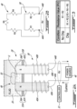
FIG. 2A is an exemplary schematic representation ofchip detector 28.Chip detector 28 may be a prong-type magnetic chip detector where magnetization is provided partially or wholly by way of electro-magnetization.Chip detector 28 may includefirst prong 35A defining first electricallyconductive terminal 36A (referred hereinafter as "first terminal 36A"), andsecond prong 35B defining second electricallyconductive terminal 36B (referred hereinafter as "second terminal 36B"). First terminal 36A and second terminal 36B may be spaced apart from each other to define chip-receiving gap G therebetween. The size(s) of gap G (i.e., the spacing between first terminal 36A and second terminal 36B) may be selected based on the chip sizes of interest. In some embodiments, the size of gap G may be between 1/64" (0.4 mm) and 1/8" (3.2 mm) for example. -
Chip detector 28 may include magnetizingcircuit 38 for magnetizing bothfirst terminal 36A andsecond terminal 36B.Magnetizing circuit 38 may includefirst coil 40A inductively coupled to first terminal 36A to generate a first generated magnetic field of a first polarity. For example,first coil 40A may be wound around firstmagnetic core 42A offirst prong 35A so that the first generated magnetic field may cause first terminal 36A to have a north (N) polarity.First coil 40A may be electrically isolated fromfirst terminal 36A via a suitable electric insulator.Second coil 40B may be inductively coupled to second terminal 36B to generate a second generated magnetic field of a second polarity opposite the first polarity. For example,second coil 40B may be wound around secondmagnetic core 42B ofsecond prong 35B so that the second generated magnetic field may cause second terminal 36B to have a south (S) polarity.Second coil 40B may be electrically isolated from second terminal 36B via a suitable electric insulator. The opposite polarities offirst terminal 36A and second terminal 36B may be achieved by havingfirst coil 40A andsecond coil 40B wound in opposite directions around firstmagnetic core 42A and secondmagnetic core 42B respectively. -
First coil 40A andsecond coil 40B may be electrically connected together in series and extend betweenfirst node 44A andsecond node 44B. An electric (e.g., direct) current supplied tofirst coil 40A andsecond coil 40B may cause the magnetization offirst terminal 36A and second terminal 36B in opposite polarities. The electric current may be supplied bypower source 46, which may include a battery or a direct current (DC) power bus ofengine 10 or of an aircraft to whichengine 10 may be mounted. In various embodiments, the electric current used for magnetization may be delivered to magnetizingcircuit 38 viacontroller 32 or separately ofcontroller 32. The electric current used for magnetization may be supplied to bothfirst coil 40A andsecond coil 40B viafirst node 44A andsecond node 44B due to the series connection betweenfirst coil 40A andsecond coil 40B. -
Chip detector 28 may includechip detection circuit 48 that is arranged in parallel with magnetizingcircuit 38.Chip detection circuit 48 may serve to detect a presence of one ormore chips 50 electrically connectingfirst terminal 36A andsecond terminal 36B.Chip detection circuit 48 may includefirst terminal 36A electrically connected tofirst node 44A viafirst conductor 49A for example.Chip detection circuit 48 may includesecond terminal 36B electrically connected tosecond node 44B viasecond conductor 49B for example.Chip detection circuit 48 may also include gap G defined between first terminal 36A andsecond terminal 36B. In other words,chip detection circuit 48 may includefirst terminal 36A, gap G andsecond terminal 36B arranged in series, and extending between the samefirst node 44A andsecond node 44B between whichfirst coil 40A andsecond coil 40B are disposed. -
First node 44A andsecond node 44B may define two connections (i.e., one supply and one return) that may be used to interface with both magnetizingcircuit 38 and with chip-detection circuit 48. In some embodiments, no additional connections may be required to interface withchip detector 28 so that a 2-pin connector may be used to interfacecontroller 32 withchip detector 28 for example. - In various embodiments,
first prong 35A andsecond prong 35B may or may not be permanent magnets. However,first prong 35A andsecond prong 35B may be made of a material that is susceptible to be magnetized viamagnetization circuit 38. In some embodiments,first prong 35A may be substantially non-magnetized in an absence of the first magnetic field generated viafirst coil 40A. In some embodiments,second prong 35B may be substantially non-magnetized in an absence of the second magnetic field generated viasecond coil 40B. In other words,first prong 35A andsecond prong 35B may be made of a non-magnetized material such as a ferromagnetic or ferrimagnetic material such as iron for example. Firstmagnetic core 42A and secondmagnetic core 42B may concentrate the magnetic flux produced byfirst coil 40A andsecond coil 40B respectively. - In some embodiments,
first prong 35A andsecond prong 35B may be of cylindrical or other suitable shape. In some embodiments, gap G may be filled with an electrically-isolating material to leave the end faces offirst terminal 36A and of second terminal 36B exposed to lubricatingfluid 26. Such configuration ofchip detector 28 may facilitate cleaning and promote durability ofchip detector 28. - During operation of
chip detector 28 whenfirst terminal 36A and second terminal 36B ofchip detector 28 are immersed in lubricatingfluid 26, the opposite polarities offirst terminal 36A and second terminal 36B may cause one or moremetallic chips 50 that are present in lubricatingfluid 26 to be magnetically drawn toward gap G between first terminal 36A andsecond terminal 36B.Chips 50 that are carried by lubricatingfluid 26 may be from metallic engine parts such as gear teeth or bearings for example. Whenchip 50 of a sufficient size, or a plurality ofchips 50, is/are attracted to and collected bychip detector 28, chip(s) 50 may electrically bridge (e.g., short-circuit) gap G defined between first terminal 36A and second terminal 36B to completechip detection circuit 48 that includes gap G. As explained further below,controller 32 or other annunciation circuitry connected tochip detector 28 may detect the capture of chip(s) 50 by way of a change in resistance value RV measured acrossfirst node 44A andsecond node 44B. Upon detection of such change in resistance value RV,controller 32 may cause annunciation 34 (shown inFIG. 1 ) to be generated. - When no
chips 50 electrically connect first terminal 36A tosecond terminal 36B,power source 46 may supply electric current to magnetizingcircuit 38 viafirst node 44A andsecond node 44B but not to chipdetection circuit 48. However, when one ormore chips 50 electrically connect first terminal 36A tosecond terminal 36B,power source 46 may supply electric current to both magnetizingcircuit 38 and to chipdetection circuit 48 viafirst node 44A andsecond node 44B. In case of the electric power delivered to magnetizingcircuit 38 andchip detection circuit 48 being of constant voltage for example, the completion ofchip detection circuit 48 by chip(s) 50 may cause some current to be delivered tochip detection circuit 48 and this may result in a decrease in current being delivered to magnetizingcircuit 38. In various embodiments, such decrease in current to magnetizingcircuit 38 may cause a change in magnetic strength associated withfirst terminal 36A andsecond terminal 36B. In other words, when one ormore chips 50 are captured bychip detector 28, the closing ofchip detection circuit 48 by chip(s) 50 may cause a decrease in current passing through magnetizingcircuit 38 so that a magnetization offirst terminal 36A and of second terminal 36B may be altered. - In some embodiments where
first terminal 36A and second terminal 36B are not permanent magnets, such change in magnetic strength may be a decrease in magnetic strength associated with the capture of chip(s) 50. In embodiments wherefirst terminal 36A and second terminal 36B are permanent magnets, such change in magnetic strength may be a decrease or an increase in magnetic strength associated with the capture of chip(s) 50 as explained in relation toFIGS. 4 and5 below. -
Chip detector 28 may include elements (e.g., resistor(s), coils/inductors) additional to those shown herein. For example, elements of magnetizingcircuit 38 and ofchip detection circuit 48 may be selected (e.g., suitably balanced) such that once thechip detection circuit 48 is closed by chip(s) 50, magnetizingcircuit 38 will continue to receive sufficient current flow frompower source 46 to produce enough magnetic strength to hold the captured chip(s) 50. Balancing (i.e., proportioning) the resistances of magnetizingcircuit 38 and ofchip detection circuit 48 may be achieved in a number of ways. For example, the resistance ofchip detection circuit 48 can be adjusted by way of one or more coils similar to those of magnetizingcircuit 38. The respective resistances ofchip detection circuit 48 and of magnetizingcircuit 38 may be adjusted by selecting a desired number of turns in each coil. The respective resistances ofchip detection circuit 48 and of magnetizingcircuit 38 may also be adjusted by selecting desired wire diameters and lengths in each circuit. The respective resistances ofchip detection circuit 48 and of magnetizingcircuit 38 may also be adjusted by the addition of one or more resistors. Any suitable combination of the above approaches may be used to adjust the respective resistances ofchip detection circuit 48 and of magnetizingcircuit 38. - In some embodiments, two or
more chip detectors 28 may be combined or integrated together in a single package to define a multi-zone chip detector. Such multi-zone chip detector may be used to detectmultiple chips 50 and used to define a legitimate chip detection only when a minimum number ofchips 50 have been detected for example. -
FIG. 2B is an equivalent electric circuit diagram 52 associated withchip detector 28 ofFIG. 2A . In reference to magnetizingcircuit 38 shown in diagram 52,first coil 40A may be represented by equivalent resistance R1, andsecond coil 40B may be represented by equivalent resistance R2 where resistances R1 and R2 may be connected in series betweenfirst node 44A andsecond node 44B. In reference tochip detection circuit 48,first prong 35A may be represented by equivalent resistance R3.Second prong 35B may be represented by equivalent resistance R4. The one ormore chips 50 captured bychip detector 28 and bridging gap G may be represented by equivalent resistance R5. Resistances R3, R4 and R5 may be connected in series betweenfirst node 44A andsecond node 44B. -
FIG. 3 is a table of measurable resistance values RV associated with no chip being captured bychip detector 28, and with one ormore chips 50 being captured bychip detector 28 and bridging gap G. For example, when no chip is captured bychip detector 28,chip detection circuit 48 may have an open-circuit state due to the absence of resistance R5 inFIG. 2B , and magnetizingcircuit 38 may provide a first known resistance (e.g., RV = R1+R2) acrossfirst node 44A andsecond node 44B that may be read by an interrogating circuit such ascontroller 32. On the other hand, when one ormore chips 50 are captured bychip detector 28 and electrically bridge gap G,chip detection circuit 48 may be closed due to the presence of resistance R5 inFIG. 2B . In this situation, the combination of magnetizingcircuit 38 and ofchip detection circuit 48 arranged in parallel may provide a second resistance (e.g., RV = R1+R2 ∥ R3+R4+R5) acrossfirst node 44A andsecond node 44B that may be read by the interrogating circuit such ascontroller 32. Such change in resistance value RV measured acrossfirst node 44A andsecond node 44B may be interpreted bycontroller 32 as a legitimate capture of one ormore chips 50 and may causeannunciation 34 to be generated. -
FIG. 4 is a schematic illustration of another exemplaryelectromagnetic chip detector 128 that may be used insystem 30.Chip detector 128 may have elements ofchip detector 28 described above, and like elements are identified using like reference numerals.Chip detector 128 may also be configured according to circuit diagram 52 ofFIG. 2B . As illustrated in callouts shown inFIG. 4 ,first prong 35A andsecond prong 35B may be permanent magnets having opposite orientations so thatfirst terminal 36A and second terminal 36B have opposite polarities. Such permanent magnets may each have their own persistent magnetic field and retain their magnetism after being removed from an external magnetic field. In various embodiments, the permanent magnets may be rare earth (e.g., neodymium or and samarium-cobalt) magnets, ferrite or alnico magnets. - In addition to being permanent magnets,
first prong 35A andsecond prong 35B may also be susceptible to magnetization by electromagnetism. Accordingly,first coil 40A may be inductively coupled tofirst terminal 36A, andsecond coil 40B may be inductively coupled tosecond terminal 36B. The winding direction offirst coil 40A aroundfirst prong 35A and the direction of current flow through magnetizingcircuit 38 may be arranged so that the first magnetic field generated byfirst coil 40A may have the same polarity as and therefore supplement (i.e., be additive to) the persistent (i.e., intrinsic) magnetic field offirst prong 35A. Similarly, the winding direction ofsecond coil 40B aroundsecond prong 35B and the direction of current flow through magnetizingcircuit 38 may be arranged so that the second magnetic field generated bysecond coil 40B may have the same polarity as and therefore supplement (i.e., be additive to) the persistent (i.e., intrinsic) magnetic field ofsecond prong 35B. - During operation, when no
chips 50 are captured bychip detector 128, the magnetic strength ofchip detector 128 provided by the permanent magnets offirst prong 35A andsecond prong 35B may be supplemented by magnetizingcircuit 38. When one ormore chips 50 are captured bychip detector 128, the closing ofchip detection circuit 48 by chip(s) 50 may cause a decrease in current passing through magnetizingcircuit 38. Such decrease in current may cause the contribution of the magnetization of thefirst terminal 36A and of second terminal 36B frommagnetization circuit 38 to be decreased after the capture of chip(s) 50 bychip detector 128. The resulting decreased magnetization may be selected to be sufficiently high to retain the captured chip(s) 50. -
FIG. 5 is a schematic illustration of another exemplaryelectromagnetic chip detector 228 that may be used insystem 30.Chip detector 228 may have elements ofchip detectors Chip detector 228 may also be configured according to circuit diagram 52 ofFIG. 2B . As illustrated in callouts shown inFIG. 5 ,first prong 35A andsecond prong 35B may be permanent magnets having opposite orientations so thatfirst terminal 36A and second terminal 36B have opposite polarities. Such permanent magnets may each have their own persistent magnetic field and retain their magnetism after being removed from an external magnetic field. In addition to being permanent magnets,first prong 35A andsecond prong 35B may also be susceptible to magnetization by electromagnetism. - Accordingly,
first coil 40A may be inductively coupled tofirst terminal 36A, andsecond coil 40B may be inductively coupled tosecond terminal 36B. - In contrast with
chip detector 128, the winding direction offirst coil 40A aroundfirst prong 35A and the direction of current flow through magnetizingcircuit 38 may be arranged so that the first magnetic field generated byfirst coil 40A may have the opposite polarity as and may therefore oppose (i.e., be subtractive from) the persistent (i.e., intrinsic) magnetic field offirst prong 35A. Similarly, the winding direction ofsecond coil 40B aroundsecond prong 35B and the direction of current flow through magnetizingcircuit 38 may be arranged so that the second magnetic field generated bysecond coil 40B may have the opposite polarity as and may therefore oppose (i.e., be subtractive from) the persistent (i.e., intrinsic) magnetic field ofsecond prong 35B. - During operation, when no
chips 50 are captured bychip detector 228, the magnetic strength ofchip detector 228 provided by the permanent magnets offirst prong 35A andsecond prong 35B may be decreased by magnetizingcircuit 38. When one ormore chips 50 are captured bychip detector 228, the closing ofchip detection circuit 48 by chip(s) 50 may cause a decrease in current passing through magnetizingcircuit 38. Such decrease in current may cause the opposing magnetization of thefirst terminal 36A and of second terminal 36B by magnetizingcircuit 38 to be decreased after the capture of chip(s) 50 bychip detector 228. This decrease in opposing magnetization may in turn cause the overall magnetic strength ofchip detector 228 to be increased due to the persistent magnetic field of the permanent magnets. In other words, the capture of chip(s) 50 may cause an increase in magnetic strength for retaining the captured chip(s) bychip detector 228. -
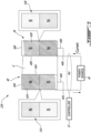
FIG. 6A is a schematic representation of another exemplaryelectromagnetic chip detector 328 that may be used insystem 30.Chip detector 328 may have elements ofchip detectors Chip detector 328 may be an axial disk-type chip detector.Chip detector 328 may includemagnetic core 42 extending and retained between first terminal 36A andsecond terminal 36B. Suitable electrically non-conductive and non-magnetically permeable isolators (not shown) may be disposed betweenmagnetic core 42 and the respectivefirst terminal 36A andsecond terminal 36B. First terminal 36A and second terminal 36B may be metallic (e.g., steel) end caps between whichmagnetic core 42 is retained. First terminal 36A and second terminal 36B may be spaced apart from each other to define chip-receiving gap G therebetween to receive one ormore chips 50. In some embodiments,magnetic core 42,first terminal 36A and second terminal 36B may be disk-shaped and may be disposed in a coaxial manner along axisA. First terminal 36A and second terminal 36B may be immersed into and in contact with lubricatingfluid 26. In various embodiments, gap G may extend partially or substantially entirely around axis A. -
Chip detector 328 may include magnetizingcircuit 38 for magnetizing bothfirst terminal 36A andsecond terminal 36B.Magnetizing circuit 38 may includecoil 40 wound around and inductively coupled tomagnetic core 42 to generate a magnetic field causingfirst terminal 36A to have a north (N) polarity and second terminal 36B to have a south (S) polarity.Coil 40 may be electrically isolated frommagnetic core 42 via a suitable electric insulator.Coil 40 may be electrically connected to and extend betweenfirst node 44A andsecond node 44B. An electric (e.g., direct) current supplied tocoil 40 may cause the magnetization offirst terminal 36A and of second terminal 36B in opposite polarities. The electric current may be supplied bypower source 46 viacontroller 32 or separately ofcontroller 32. -
Chip detector 328 may includechip detection circuit 48 that is arranged in parallel with magnetizingcircuit 38.Chip detection circuit 48 may serve to detect a presence of one ormore chips 50 electrically connectingfirst terminal 36A and second terminal 36B together.Chip detection circuit 48 may includefirst terminal 36A electrically connected tofirst node 44A viafirst conductor 49A for example.Chip detection circuit 48 may includesecond terminal 36B electrically connected tosecond node 44B viasecond conductor 49B for example.Chip detection circuit 48 may also include gap G defined between first terminal 36A andsecond terminal 36B. In other words,chip detection circuit 48 may includefirst terminal 36A, gap G andsecond terminal 36B arranged in series, and extending between the samefirst node 44A andsecond node 44B between whichcoil 40 is disposed. -
First node 44A andsecond node 44B may define two connections (i.e., one supply and one return) that may be used to interface with both magnetizingcircuit 38 and with chip-detection circuit 48. In some embodiments, no additional connections may be required to interface withchip detector 328 so that a 2-pin connector may be used to interfacecontroller 32 withchip detector 328 for example. - In various embodiments,
magnetic core 42 may or may not be a permanent magnet. However,magnetic core 42 may be made of a material that is suitable for concentrating magnetic flux generated usingcoil 40. In some embodiments,magnetic core 42 may be made of a non-magnetized material. In some embodiments,magnetic core 42 may be a permanent magnet producing a persistent magnetic field. Similarly to chipdetectors FIGS. 4 and5 , the magnetic field generated usingcoil 40 and the persistent magnetic field of the permanent magnet may be arranged in an additive or subtractive manner. For example, in various embodiments, the magnetic field generated usingcoil 40 may supplement or oppose the persistent magnetic field of the permanent magnet to achieve either a decrease or an increase in magnetic strength ofdetector 328 after the capture of chip(s) 50. - During operation of
chip detector 328 whenfirst terminal 36A and second terminal 36B ofchip detector 328 are immersed in lubricatingfluid 26, the opposite polarities offirst terminal 36A and second terminal 36B may cause one or moremetallic chips 50 that are present in lubricatingfluid 26 to be magnetically drawn toward gap G between first terminal 36A andsecond terminal 36B. Whenchip 50 of a sufficient size, or a plurality ofchips 50, is/are attracted tochip detector 328, chip(s) 50 may electrically bridge (e.g., short-circuit) gap G defined between first terminal 36A and second terminal 36B to completechip detection circuit 48 that includesgap G. Controller 32 or other annunciation circuitry connected tochip detector 328 may detect the capture of chip(s) 50 by way of a change in resistance value RV measured acrossfirst node 44A andsecond node 44B. Upon detection of such change in resistance value RV,controller 32 may cause annunciation 34 (shown inFIG. 1 ) to be generated.Chip detector 328 may include elements (e.g., resistor(s), coils/inductors) additional to those shown herein to adjust the respective resistances ofchip detection circuit 48 and of magnetizingcircuit 38 to achieve a suitable resistance proportion between magnetizingcircuit 38 andchip detection circuit 48 as explained above. - When no
chips 50 electrically connect first terminal 36A tosecond terminal 36B,power source 46 may supply electric current to magnetizingcircuit 38 viafirst node 44A andsecond node 44B but not to chipdetection circuit 48. However, when one ormore chips 50 electrically connect first terminal 36A tosecond terminal 36B,power source 46 may supply electric current to both magnetizingcircuit 38 and to chipdetection circuit 48 viafirst node 44A andsecond node 44B. -
FIG. 6B is an equivalent electric circuit diagram 152 associated withchip detector 328 ofFIG. 6A . In contrast with diagram 52 ofFIG. 2B , diagram 152 may not include resistance R2 since only onecoil 40 is required to magnetize bothfirst terminal 36A and second terminal 36B with opposite polarities. In reference to magnetizingcircuit 38,coil 40 may be represented by equivalent resistance R1 disposed betweenfirst node 44A andsecond node 44B. In reference tochip detection circuit 48,first terminal 36A may be represented by equivalent resistance R3.Second terminal 36B may be represented by equivalent resistance R4. The one ormore chips 50 captured bychip detector 328 and bridging gap G may be represented by equivalent resistance R5. Resistances R3, R4 and R5 may be connected in series betweenfirst node 44A andsecond node 44B. Resistances R3, R4 and R5 may be connected in parallel with resistance R1. -
FIG. 7 is a table of measurable resistance values RV associated with no chip being captured bychip detector 328, and with one ormore chips 50 being captured bychip detector 328 and bridging gap G. For example, when no chip is captured bychip detector 328,chip detection circuit 48 may have an open-circuit state due to the absence of resistance R5 inFIG. 6B , and magnetizingcircuit 38 may provide a first known resistance (e.g., RV = R1) acrossfirst node 44A andsecond node 44B that may be read by an interrogating circuit such ascontroller 32. On the other hand, when one ormore chips 50 are captured bychip detector 328 and electrically bridge gap G,chip detection circuit 48 may be closed due to the presence of resistance R5 inFIG. 6B . In this situation, the combination of magnetizingcircuit 38 and ofchip detection circuit 48 arranged in parallel may provide a second resistance (e.g., RV = R1 ∥ R3+R4+R5) acrossfirst node 44A andsecond node 44B that may be read by the interrogating circuit such ascontroller 32. Such change in resistance value RV measured acrossfirst node 44A andsecond node 44B may be interpreted bycontroller 32 as a legitimate capture of one ormore chips 50 and may causeannunciation 34 to be generated. -
FIG. 8 is a flow diagram ofmethod 100 of detecting one or moremetallic chips 50 in engine fluid ofengine 10.Method 100 may be performed using any one ofchip detectors Method 100 may include other steps or actions disclosed herein.Method 100 may include elements ofchip detectors method 100 may include: - supplying an electric current to magnetizing
circuit 38 extending betweenfirst node 44A andsecond node 44B to magnetize bothfirst terminal 36A and second terminal 36B spaced apart from each other to define gap G therebetween (block 102); and - detecting a change in resistance value RV across
first nodes 44A andsecond node 44B, the change in resistance value RV being indicative of a capture of chip(s) 50 bychip detector second terminal 36B,first terminal 36A being electrically connected tofirst node 44A, and second terminal 36B being electrically connected tosecond node 44B (block 104). - In some embodiments,
method 100 may include altering a magnetization offirst terminal 36A and of second terminal 36B after the capture of chip(s) 50 bychip detectors first terminal 36A and of second terminal 36B may include reducing the magnetization offirst terminal 36A and of second terminal 36B ofchip detectors first terminal 36A and of second terminal 36B may include increasing the magnetization offirst terminal 36A and of second terminal 36B ofchip detectors - The embodiments described in this document provide non-limiting examples of possible implementations of the present technology. Upon review of the present disclosure, a person of ordinary skill in the art will recognize that changes may be made to the embodiments described herein without departing from the scope of the present technology.
Claims (15)
- An electromagnetic chip detector (28; 128; 228; 328) for detecting a metallic chip (50) in lubricating fluid of an engine (10), the electromagnetic chip detector (28...328) comprising:a first electrically conductive terminal (36A);a second electrically conductive terminal (36B) spaced apart from the first electrically conductive terminal (36A) to define a chip-receiving gap (G) therebetween;a magnetizing circuit (38) including:a first coil (40A) inductively coupled to the first electrically conductive terminal (36A) to generate a first generated magnetic field of a first polarity; anda second coil (40B) inductively coupled to the second electrically conductive terminal (36B) to generate a second generated magnetic field of a second polarity opposite the first polarity, the first coil (40A) and the second coil (40B) being electrically connected in series between a first node (44A) and a second node (44B);a chip detection circuit (48) in parallel with the magnetizing circuit (38), the chip detection circuit (48) including:the first electrically conductive terminal (36A) electrically connected to the first node (44A);the second electrically conductive terminal (36B) electrically connected to the second node (44B); andthe chip-receiving gap (G) defined between the first electrically conductive terminal (36A) and the second electrically conductive terminal (36B).
- The electromagnetic chip detector as defined in claim 1, wherein the first electrically conductive terminal (36A) is non-magnetized in an absence of the first generated magnetic field, and/or the second electrically conductive terminal (36B) is non-magnetized in an absence of the second generated magnetic field.
- The electromagnetic chip detector as defined in claim 1, wherein:the first electrically conductive terminal (36A) is a first permanent magnet having a first persistent magnetic field; andthe first generated magnetic field supplements the first persistent magnetic field.
- The electromagnetic chip detector as defined in claim 1 or 3, wherein:the second electrically conductive terminal (36B) is a second permanent magnet having a second persistent magnetic field; andthe second generated magnetic field supplements the second persistent magnetic field.
- The electromagnetic chip detector as defined in claim 1, wherein the first electrically conductive terminal (36A) is a first permanent magnet having a first persistent magnetic field, and the first generated magnetic field opposes the first persistent magnetic field, and/or the second electrically conductive terminal (36B) is a second permanent magnet having a second persistent magnetic field, and the second generated magnetic field opposes the second persistent magnetic field.
- The electromagnetic chip detector as defined in any preceding claim, comprising a power source (46) configured to supply electric current to both the magnetizing circuit (38) and the chip detection circuit (48) via the first node (44A) and the second node (44B) when a chip (50) electrically connects the first electrically conductive terminal (36A) to the second electrically conductive terminal (36B).
- An electromagnetic chip detector (28; 128; 228; 328) for detecting a metallic chip (50) in engine fluid of an engine (10), the electromagnetic chip detector (28...328) comprising:a first electrically conductive terminal (36A);a second electrically conductive terminal (36B) spaced apart from the first electrically conductive terminal (36A) to define a chip-receiving gap (G) therebetween;a first circuit (38) magnetizing the first electrically conductive terminal (36A) to have a first polarity and magnetizing the second electrically conductive terminal (36B) to have a second polarity opposite the first polarity;a second circuit (48) detecting a presence of a chip (50) electrically connecting the first electrically conductive terminal (36A) and the second electrically conductive terminal (36B) together; anda power source (46) supplying electric current to both the first circuit (38) and the second circuit (48) via a first node (44A) and a second node (44B) when the chip (50) electrically connects the first electrically conductive terminal (36A) to the second electrically conductive terminal (36B).
- The electromagnetic chip detector as defined in claim 7, comprising a magnetic core (42) extending between the first electrically conductive terminal (36A) and the second electrically conductive terminal (36B), the first circuit (38) including a coil (40) inductively coupled to the magnetic core (42) to generate a generated magnetic field, and/or the first electrically conductive terminal (36A) and the second electrically conductive terminal (36B) are both disk-shaped.
- The electromagnetic chip detector as defined in claim 8, wherein the magnetic core (42) is made of a non-magnetized material.
- The electromagnetic chip detector as defined in claim 8 wherein:the magnetic core (42) is a permanent magnet producing a persistent magnetic field; andthe generated magnetic field supplements the persistent magnetic field or opposes the persistent magnetic field.
- The electromagnetic chip detector as defined in claim 7, wherein the first circuit (38) includes:a first coil (40A) inductively coupled to a first prong (35A) defining the first electrically conductive terminal (36A); anda second coil (40B) inductively coupled to the a second prong (35B) defining the second electrically conductive terminal (36B), the first coil (40A) and the second coil (40B) being electrically connected in series between the first node (44A) and the second node (44B).
- The electromagnetic chip detector as defined in any of claims 7 to 11, comprising a controller (32) operatively connected to the electromagnetic chip detector (28...328), the controller (32) detecting an electric resistance (RV) across the first node (44A) and the second node (44B).
- A method of detecting a metallic chip (50) in engine fluid (26) of an engine (10) using an electromagnetic chip detector (28; 128; 228; 328), the method comprising:supplying an electric current to a circuit (38) extending between a first node (44A) and a second node (44B) to magnetize both a first electrically conductive terminal (36A) and a second electrically conductive terminal (36B) spaced apart from each other to define a chip-receiving gap (G) therebetween; anddetecting a change in resistance across the first node (44A) and the second node (44B), the change in resistance being indicative of a capture of the metallic chip (50) by the electromagnetic chip detector (28...328), the metallic chip (50) electrically connecting the first electrically conductive terminal (36A) to the second electrically conductive terminal (36B), the first electrically conductive terminal (36A) being electrically connected to the first node (44A), and the second electrically conductive terminal (36B) being electrically connected to the second node (44B).
- The method as defined in claim 13, comprising altering a magnetization of the first electrically conductive terminal (36A) and of the second electrically conductive terminal (36B) after the capture of the metallic chip (50) by the electromagnetic chip detector (28...328).
- The method as defined in claim 14, wherein altering the magnetization of the first electrically conductive terminal (36A) and of the second electrically conductive terminal (36B) includes reducing the magnetization of the first electrically conductive terminal (36A) and of the second electrically conductive terminal (36B) or increasing the magnetization of the first electrically conductive terminal (36A) and of the second electrically conductive terminal (36B).
Applications Claiming Priority (1)
| Application Number | Priority Date | Filing Date | Title |
|---|---|---|---|
| US17/577,190 US11906504B2 (en) | 2022-01-17 | 2022-01-17 | Electromagnetic chip detector |
Publications (1)
| Publication Number | Publication Date |
|---|---|
| EP4212861A1 true EP4212861A1 (en) | 2023-07-19 |
Family
ID=84981941
Family Applications (1)
| Application Number | Title | Priority Date | Filing Date |
|---|---|---|---|
| EP23151999.2A Pending EP4212861A1 (en) | 2022-01-17 | 2023-01-17 | Electromagnetic chip detector |
Country Status (3)
| Country | Link |
|---|---|
| US (1) | US11906504B2 (en) |
| EP (1) | EP4212861A1 (en) |
| CA (1) | CA3186216A1 (en) |
Families Citing this family (3)
| Publication number | Priority date | Publication date | Assignee | Title |
|---|---|---|---|---|
| US12196548B2 (en) | 2021-08-17 | 2025-01-14 | Pratt & Whitney Canada Corp. | Method and system for sizing a chip in engine fluid |
| US12216084B2 (en) * | 2022-03-18 | 2025-02-04 | Dana Italia S.R.L. | Metal debris sensor for oil with temperature compensation |
| US12535446B2 (en) | 2023-05-24 | 2026-01-27 | Pratt & Whitney Canada Corp. | Capacitive chip detector |
Citations (2)
| Publication number | Priority date | Publication date | Assignee | Title |
|---|---|---|---|---|
| DE102017204304A1 (en) * | 2017-03-15 | 2018-09-20 | Zf Friedrichshafen Ag | Apparatus for measuring the amount of metallic particles in a liquid |
| US20210262897A1 (en) * | 2020-02-24 | 2021-08-26 | Pratt & Whitney Canada Corp. | Magnetic chip detector and method of use |
Family Cites Families (8)
| Publication number | Priority date | Publication date | Assignee | Title |
|---|---|---|---|---|
| US5179346A (en) * | 1991-05-24 | 1993-01-12 | Caterpillar, Inc. | Conductive particle sensor using a magnet |
| US5674401A (en) * | 1991-12-11 | 1997-10-07 | Computational Systems, Inc. | Oil monitor with magnetic field |
| US10648361B2 (en) * | 2016-07-26 | 2020-05-12 | United Technologies Corporation | Oil debris monitor with sequential coil system and associated algorithms for particle confirmation |
| US10705039B2 (en) * | 2017-03-27 | 2020-07-07 | Nabtesco Corporation | Sensor for detecting magnetic powders in a lubricant |
| US10197488B2 (en) | 2017-06-15 | 2019-02-05 | Pratt & Whitney Canada Corp. | Systems and methods for detecting chips in fluid of aircraft engine |
| US10866201B2 (en) | 2017-11-29 | 2020-12-15 | Pratt & Whitney Canada Corp. | Lubricant debris monitoring system for gas turbine engine |
| BE1028174B1 (en) | 2020-03-30 | 2021-10-25 | Safran Aero Boosters | DEBRIS ATTRACTION AND DETECTION MODULE |
| US11549933B2 (en) | 2020-02-24 | 2023-01-10 | Pratt & Whitney Canada Corp. | Magnetic chip detector and method of use |
-
2022
- 2022-01-17 US US17/577,190 patent/US11906504B2/en active Active
-
2023
- 2023-01-10 CA CA3186216A patent/CA3186216A1/en active Pending
- 2023-01-17 EP EP23151999.2A patent/EP4212861A1/en active Pending
Patent Citations (2)
| Publication number | Priority date | Publication date | Assignee | Title |
|---|---|---|---|---|
| DE102017204304A1 (en) * | 2017-03-15 | 2018-09-20 | Zf Friedrichshafen Ag | Apparatus for measuring the amount of metallic particles in a liquid |
| US20210262897A1 (en) * | 2020-02-24 | 2021-08-26 | Pratt & Whitney Canada Corp. | Magnetic chip detector and method of use |
Also Published As
| Publication number | Publication date |
|---|---|
| US20230228731A1 (en) | 2023-07-20 |
| US11906504B2 (en) | 2024-02-20 |
| CA3186216A1 (en) | 2023-07-17 |
Similar Documents
| Publication | Publication Date | Title |
|---|---|---|
| CA3186216A1 (en) | Electromagnetic chip detector | |
| CA2853064C (en) | Magnetic chip detector/collector | |
| US8074493B2 (en) | Pre-signaling magnetic plug | |
| US11448636B2 (en) | Magnetic chip detector | |
| US11549933B2 (en) | Magnetic chip detector and method of use | |
| CN112858464B (en) | Magnetic metal particle detection sensor and system | |
| US12203920B2 (en) | Multi-zone magnetic chip detector | |
| JP2024133183A (en) | Electrical machine including a device for forcibly demagnetizing a permanent magnet | |
| US8018225B2 (en) | System and method for sensing the periodic position of an object | |
| CA2735220C (en) | System and method for sensing the periodic position of an object | |
| US11499890B2 (en) | Magnetic chip detector and method of use | |
| CN115552101B (en) | Analytical equipment for detecting solid particles in lubricants | |
| US7948229B2 (en) | High temperature electronics for passive eddy current sensors | |
| US12535446B2 (en) | Capacitive chip detector | |
| CN212459743U (en) | Initial velocity sensor | |
| EP4432524A1 (en) | Electric machine | |
| CN117339757A (en) | Lubricating oil on-line particulate matter removing system | |
| CN105127149A (en) | Purification method and device for variable-reluctance transducer | |
| Seaplane et al. | Recent Technical Developments | |
| Manly | Automobile starting, lighting and ignition: a practical instruction and reference work on construction, operation and care of all makes and types of automobile electrical equipment | |
| GB427381A (en) | Improvements in or relating to combined electrical regulators and automatic cut-outs |
Legal Events
| Date | Code | Title | Description |
|---|---|---|---|
| PUAI | Public reference made under article 153(3) epc to a published international application that has entered the european phase |
Free format text: ORIGINAL CODE: 0009012 |
|
| STAA | Information on the status of an ep patent application or granted ep patent |
Free format text: STATUS: THE APPLICATION HAS BEEN PUBLISHED |
|
| AK | Designated contracting states |
Kind code of ref document: A1 Designated state(s): AL AT BE BG CH CY CZ DE DK EE ES FI FR GB GR HR HU IE IS IT LI LT LU LV MC ME MK MT NL NO PL PT RO RS SE SI SK SM TR |
|
| STAA | Information on the status of an ep patent application or granted ep patent |
Free format text: STATUS: REQUEST FOR EXAMINATION WAS MADE |
|
| 17P | Request for examination filed |
Effective date: 20240118 |
|
| RBV | Designated contracting states (corrected) |
Designated state(s): AL AT BE BG CH CY CZ DE DK EE ES FI FR GB GR HR HU IE IS IT LI LT LU LV MC ME MK MT NL NO PL PT RO RS SE SI SK SM TR |
|
| STAA | Information on the status of an ep patent application or granted ep patent |
Free format text: STATUS: EXAMINATION IS IN PROGRESS |
|
| 17Q | First examination report despatched |
Effective date: 20250715 |