EP4210166A2 - Semiconductor package with integrated antenna and shielding pillars - Google Patents
Semiconductor package with integrated antenna and shielding pillars Download PDFInfo
- Publication number
- EP4210166A2 EP4210166A2 EP22211882.0A EP22211882A EP4210166A2 EP 4210166 A2 EP4210166 A2 EP 4210166A2 EP 22211882 A EP22211882 A EP 22211882A EP 4210166 A2 EP4210166 A2 EP 4210166A2
- Authority
- EP
- European Patent Office
- Prior art keywords
- base film
- disposed
- die
- micrometers
- semiconductor package
- Prior art date
- Legal status (The legal status is an assumption and is not a legal conclusion. Google has not performed a legal analysis and makes no representation as to the accuracy of the status listed.)
- Pending
Links
Images






Classifications
-
- H—ELECTRICITY
- H10—SEMICONDUCTOR DEVICES; ELECTRIC SOLID-STATE DEVICES NOT OTHERWISE PROVIDED FOR
- H10W—GENERIC PACKAGES, INTERCONNECTIONS, CONNECTORS OR OTHER CONSTRUCTIONAL DETAILS OF DEVICES COVERED BY CLASS H10
- H10W70/00—Package substrates; Interposers; Redistribution layers [RDL]
- H10W70/01—Manufacture or treatment
- H10W70/05—Manufacture or treatment of insulating or insulated package substrates, or of interposers, or of redistribution layers
- H10W70/08—Manufacture or treatment of insulating or insulated package substrates, or of interposers, or of redistribution layers by depositing layers on the chip or wafer, e.g. "chip-first" RDLs
- H10W70/09—Manufacture or treatment of insulating or insulated package substrates, or of interposers, or of redistribution layers by depositing layers on the chip or wafer, e.g. "chip-first" RDLs extending onto an encapsulation that laterally surrounds the chip or wafer, e.g. fan-out wafer level package [FOWLP] RDLs
-
- H—ELECTRICITY
- H10—SEMICONDUCTOR DEVICES; ELECTRIC SOLID-STATE DEVICES NOT OTHERWISE PROVIDED FOR
- H10W—GENERIC PACKAGES, INTERCONNECTIONS, CONNECTORS OR OTHER CONSTRUCTIONAL DETAILS OF DEVICES COVERED BY CLASS H10
- H10W20/00—Interconnections in chips, wafers or substrates
- H10W20/40—Interconnections external to wafers or substrates, e.g. back-end-of-line [BEOL] metallisations or vias connecting to gate electrodes
- H10W20/482—Interconnections external to wafers or substrates, e.g. back-end-of-line [BEOL] metallisations or vias connecting to gate electrodes for individual devices provided for in groups H10D8/00 - H10D48/00, e.g. for power transistors
- H10W20/484—Interconnections having extended contours, e.g. pads having mesh shape or interconnections comprising connected parallel stripes
-
- H—ELECTRICITY
- H01—ELECTRIC ELEMENTS
- H01Q—ANTENNAS, i.e. RADIO AERIALS
- H01Q1/00—Details of, or arrangements associated with, antennas
- H01Q1/12—Supports; Mounting means
- H01Q1/22—Supports; Mounting means by structural association with other equipment or articles
- H01Q1/2283—Supports; Mounting means by structural association with other equipment or articles mounted in or on the surface of a semiconductor substrate as a chip-type antenna or integrated with other components into an IC package
-
- H—ELECTRICITY
- H01—ELECTRIC ELEMENTS
- H01Q—ANTENNAS, i.e. RADIO AERIALS
- H01Q1/00—Details of, or arrangements associated with, antennas
- H01Q1/36—Structural form of radiating elements, e.g. cone, spiral, umbrella; Particular materials used therewith
- H01Q1/38—Structural form of radiating elements, e.g. cone, spiral, umbrella; Particular materials used therewith formed by a conductive layer on an insulating support
-
- H—ELECTRICITY
- H10—SEMICONDUCTOR DEVICES; ELECTRIC SOLID-STATE DEVICES NOT OTHERWISE PROVIDED FOR
- H10W—GENERIC PACKAGES, INTERCONNECTIONS, CONNECTORS OR OTHER CONSTRUCTIONAL DETAILS OF DEVICES COVERED BY CLASS H10
- H10W42/00—Arrangements for protection of devices
- H10W42/20—Arrangements for protection of devices protecting against electromagnetic or particle radiation, e.g. light, X-rays, gamma-rays or electrons
-
- H—ELECTRICITY
- H10—SEMICONDUCTOR DEVICES; ELECTRIC SOLID-STATE DEVICES NOT OTHERWISE PROVIDED FOR
- H10W—GENERIC PACKAGES, INTERCONNECTIONS, CONNECTORS OR OTHER CONSTRUCTIONAL DETAILS OF DEVICES COVERED BY CLASS H10
- H10W44/00—Electrical arrangements for controlling or matching impedance
- H10W44/20—Electrical arrangements for controlling or matching impedance at high-frequency [HF] or radio frequency [RF]
-
- H—ELECTRICITY
- H10—SEMICONDUCTOR DEVICES; ELECTRIC SOLID-STATE DEVICES NOT OTHERWISE PROVIDED FOR
- H10W—GENERIC PACKAGES, INTERCONNECTIONS, CONNECTORS OR OTHER CONSTRUCTIONAL DETAILS OF DEVICES COVERED BY CLASS H10
- H10W70/00—Package substrates; Interposers; Redistribution layers [RDL]
- H10W70/60—Insulating or insulated package substrates; Interposers; Redistribution layers
- H10W70/62—Insulating or insulated package substrates; Interposers; Redistribution layers characterised by their interconnections
- H10W70/65—Shapes or dispositions of interconnections
-
- H—ELECTRICITY
- H10—SEMICONDUCTOR DEVICES; ELECTRIC SOLID-STATE DEVICES NOT OTHERWISE PROVIDED FOR
- H10W—GENERIC PACKAGES, INTERCONNECTIONS, CONNECTORS OR OTHER CONSTRUCTIONAL DETAILS OF DEVICES COVERED BY CLASS H10
- H10W70/00—Package substrates; Interposers; Redistribution layers [RDL]
- H10W70/60—Insulating or insulated package substrates; Interposers; Redistribution layers
- H10W70/67—Insulating or insulated package substrates; Interposers; Redistribution layers characterised by their insulating layers or insulating parts
- H10W70/68—Shapes or dispositions thereof
- H10W70/685—Shapes or dispositions thereof comprising multiple insulating layers
-
- H—ELECTRICITY
- H10—SEMICONDUCTOR DEVICES; ELECTRIC SOLID-STATE DEVICES NOT OTHERWISE PROVIDED FOR
- H10W—GENERIC PACKAGES, INTERCONNECTIONS, CONNECTORS OR OTHER CONSTRUCTIONAL DETAILS OF DEVICES COVERED BY CLASS H10
- H10W72/00—Interconnections or connectors in packages
- H10W72/50—Bond wires
-
- H—ELECTRICITY
- H10—SEMICONDUCTOR DEVICES; ELECTRIC SOLID-STATE DEVICES NOT OTHERWISE PROVIDED FOR
- H10W—GENERIC PACKAGES, INTERCONNECTIONS, CONNECTORS OR OTHER CONSTRUCTIONAL DETAILS OF DEVICES COVERED BY CLASS H10
- H10W74/00—Encapsulations, e.g. protective coatings
- H10W74/10—Encapsulations, e.g. protective coatings characterised by their shape or disposition
- H10W74/111—Encapsulations, e.g. protective coatings characterised by their shape or disposition the semiconductor body being completely enclosed
- H10W74/114—Encapsulations, e.g. protective coatings characterised by their shape or disposition the semiconductor body being completely enclosed by a substrate and the encapsulations
- H10W74/117—Encapsulations, e.g. protective coatings characterised by their shape or disposition the semiconductor body being completely enclosed by a substrate and the encapsulations the substrate having spherical bumps for external connection
-
- H—ELECTRICITY
- H10—SEMICONDUCTOR DEVICES; ELECTRIC SOLID-STATE DEVICES NOT OTHERWISE PROVIDED FOR
- H10W—GENERIC PACKAGES, INTERCONNECTIONS, CONNECTORS OR OTHER CONSTRUCTIONAL DETAILS OF DEVICES COVERED BY CLASS H10
- H10W74/00—Encapsulations, e.g. protective coatings
- H10W74/10—Encapsulations, e.g. protective coatings characterised by their shape or disposition
- H10W74/111—Encapsulations, e.g. protective coatings characterised by their shape or disposition the semiconductor body being completely enclosed
- H10W74/121—Encapsulations, e.g. protective coatings characterised by their shape or disposition the semiconductor body being completely enclosed by multiple encapsulations, e.g. by a thin protective coating and a thick encapsulation
-
- H—ELECTRICITY
- H10—SEMICONDUCTOR DEVICES; ELECTRIC SOLID-STATE DEVICES NOT OTHERWISE PROVIDED FOR
- H10W—GENERIC PACKAGES, INTERCONNECTIONS, CONNECTORS OR OTHER CONSTRUCTIONAL DETAILS OF DEVICES COVERED BY CLASS H10
- H10W90/00—Package configurations
- H10W90/401—Package configurations characterised by multiple insulating or insulated package substrates, interposers or RDLs
-
- H—ELECTRICITY
- H10—SEMICONDUCTOR DEVICES; ELECTRIC SOLID-STATE DEVICES NOT OTHERWISE PROVIDED FOR
- H10W—GENERIC PACKAGES, INTERCONNECTIONS, CONNECTORS OR OTHER CONSTRUCTIONAL DETAILS OF DEVICES COVERED BY CLASS H10
- H10W90/00—Package configurations
- H10W90/701—Package configurations characterised by the relative positions of pads or connectors relative to package parts
-
- H—ELECTRICITY
- H10—SEMICONDUCTOR DEVICES; ELECTRIC SOLID-STATE DEVICES NOT OTHERWISE PROVIDED FOR
- H10P—GENERIC PROCESSES OR APPARATUS FOR THE MANUFACTURE OR TREATMENT OF DEVICES COVERED BY CLASS H10
- H10P72/00—Handling or holding of wafers, substrates or devices during manufacture or treatment thereof
- H10P72/70—Handling or holding of wafers, substrates or devices during manufacture or treatment thereof for supporting or gripping
- H10P72/74—Handling or holding of wafers, substrates or devices during manufacture or treatment thereof for supporting or gripping using temporarily an auxiliary support
- H10P72/7426—Handling or holding of wafers, substrates or devices during manufacture or treatment thereof for supporting or gripping using temporarily an auxiliary support used as a support during build up manufacturing of active devices
-
- H—ELECTRICITY
- H10—SEMICONDUCTOR DEVICES; ELECTRIC SOLID-STATE DEVICES NOT OTHERWISE PROVIDED FOR
- H10W—GENERIC PACKAGES, INTERCONNECTIONS, CONNECTORS OR OTHER CONSTRUCTIONAL DETAILS OF DEVICES COVERED BY CLASS H10
- H10W44/00—Electrical arrangements for controlling or matching impedance
- H10W44/20—Electrical arrangements for controlling or matching impedance at high-frequency [HF] or radio frequency [RF]
- H10W44/203—Electrical connections
- H10W44/209—Vertical interconnections, e.g. vias
-
- H—ELECTRICITY
- H10—SEMICONDUCTOR DEVICES; ELECTRIC SOLID-STATE DEVICES NOT OTHERWISE PROVIDED FOR
- H10W—GENERIC PACKAGES, INTERCONNECTIONS, CONNECTORS OR OTHER CONSTRUCTIONAL DETAILS OF DEVICES COVERED BY CLASS H10
- H10W44/00—Electrical arrangements for controlling or matching impedance
- H10W44/20—Electrical arrangements for controlling or matching impedance at high-frequency [HF] or radio frequency [RF]
- H10W44/241—Electrical arrangements for controlling or matching impedance at high-frequency [HF] or radio frequency [RF] for passive devices or passive elements
- H10W44/248—Electrical arrangements for controlling or matching impedance at high-frequency [HF] or radio frequency [RF] for passive devices or passive elements for antennas
-
- H—ELECTRICITY
- H10—SEMICONDUCTOR DEVICES; ELECTRIC SOLID-STATE DEVICES NOT OTHERWISE PROVIDED FOR
- H10W—GENERIC PACKAGES, INTERCONNECTIONS, CONNECTORS OR OTHER CONSTRUCTIONAL DETAILS OF DEVICES COVERED BY CLASS H10
- H10W70/00—Package substrates; Interposers; Redistribution layers [RDL]
- H10W70/099—Connecting interconnections to insulating or insulated package substrates, interposers or redistribution layers
-
- H—ELECTRICITY
- H10—SEMICONDUCTOR DEVICES; ELECTRIC SOLID-STATE DEVICES NOT OTHERWISE PROVIDED FOR
- H10W—GENERIC PACKAGES, INTERCONNECTIONS, CONNECTORS OR OTHER CONSTRUCTIONAL DETAILS OF DEVICES COVERED BY CLASS H10
- H10W70/00—Package substrates; Interposers; Redistribution layers [RDL]
- H10W70/60—Insulating or insulated package substrates; Interposers; Redistribution layers
-
- H—ELECTRICITY
- H10—SEMICONDUCTOR DEVICES; ELECTRIC SOLID-STATE DEVICES NOT OTHERWISE PROVIDED FOR
- H10W—GENERIC PACKAGES, INTERCONNECTIONS, CONNECTORS OR OTHER CONSTRUCTIONAL DETAILS OF DEVICES COVERED BY CLASS H10
- H10W70/00—Package substrates; Interposers; Redistribution layers [RDL]
- H10W70/60—Insulating or insulated package substrates; Interposers; Redistribution layers
- H10W70/611—Insulating or insulated package substrates; Interposers; Redistribution layers for connecting multiple chips together
- H10W70/614—Insulating or insulated package substrates; Interposers; Redistribution layers for connecting multiple chips together the multiple chips being integrally enclosed
-
- H—ELECTRICITY
- H10—SEMICONDUCTOR DEVICES; ELECTRIC SOLID-STATE DEVICES NOT OTHERWISE PROVIDED FOR
- H10W—GENERIC PACKAGES, INTERCONNECTIONS, CONNECTORS OR OTHER CONSTRUCTIONAL DETAILS OF DEVICES COVERED BY CLASS H10
- H10W70/00—Package substrates; Interposers; Redistribution layers [RDL]
- H10W70/60—Insulating or insulated package substrates; Interposers; Redistribution layers
- H10W70/62—Insulating or insulated package substrates; Interposers; Redistribution layers characterised by their interconnections
- H10W70/65—Shapes or dispositions of interconnections
- H10W70/652—Cross-sectional shapes
- H10W70/6528—Cross-sectional shapes of the portions that connect to chips, wafers or package parts
-
- H—ELECTRICITY
- H10—SEMICONDUCTOR DEVICES; ELECTRIC SOLID-STATE DEVICES NOT OTHERWISE PROVIDED FOR
- H10W—GENERIC PACKAGES, INTERCONNECTIONS, CONNECTORS OR OTHER CONSTRUCTIONAL DETAILS OF DEVICES COVERED BY CLASS H10
- H10W70/00—Package substrates; Interposers; Redistribution layers [RDL]
- H10W70/60—Insulating or insulated package substrates; Interposers; Redistribution layers
- H10W70/67—Insulating or insulated package substrates; Interposers; Redistribution layers characterised by their insulating layers or insulating parts
- H10W70/69—Insulating materials thereof
- H10W70/695—Organic materials
-
- H—ELECTRICITY
- H10—SEMICONDUCTOR DEVICES; ELECTRIC SOLID-STATE DEVICES NOT OTHERWISE PROVIDED FOR
- H10W—GENERIC PACKAGES, INTERCONNECTIONS, CONNECTORS OR OTHER CONSTRUCTIONAL DETAILS OF DEVICES COVERED BY CLASS H10
- H10W72/00—Interconnections or connectors in packages
- H10W72/071—Connecting or disconnecting
- H10W72/072—Connecting or disconnecting of bump connectors
- H10W72/07251—Connecting or disconnecting of bump connectors characterised by changes in properties of the bump connectors during connecting
- H10W72/07252—Connecting or disconnecting of bump connectors characterised by changes in properties of the bump connectors during connecting changes in structures or sizes
-
- H—ELECTRICITY
- H10—SEMICONDUCTOR DEVICES; ELECTRIC SOLID-STATE DEVICES NOT OTHERWISE PROVIDED FOR
- H10W—GENERIC PACKAGES, INTERCONNECTIONS, CONNECTORS OR OTHER CONSTRUCTIONAL DETAILS OF DEVICES COVERED BY CLASS H10
- H10W72/00—Interconnections or connectors in packages
- H10W72/071—Connecting or disconnecting
- H10W72/073—Connecting or disconnecting of die-attach connectors
-
- H—ELECTRICITY
- H10—SEMICONDUCTOR DEVICES; ELECTRIC SOLID-STATE DEVICES NOT OTHERWISE PROVIDED FOR
- H10W—GENERIC PACKAGES, INTERCONNECTIONS, CONNECTORS OR OTHER CONSTRUCTIONAL DETAILS OF DEVICES COVERED BY CLASS H10
- H10W72/00—Interconnections or connectors in packages
- H10W72/20—Bump connectors, e.g. solder bumps or copper pillars; Dummy bumps; Thermal bumps
- H10W72/221—Structures or relative sizes
-
- H—ELECTRICITY
- H10—SEMICONDUCTOR DEVICES; ELECTRIC SOLID-STATE DEVICES NOT OTHERWISE PROVIDED FOR
- H10W—GENERIC PACKAGES, INTERCONNECTIONS, CONNECTORS OR OTHER CONSTRUCTIONAL DETAILS OF DEVICES COVERED BY CLASS H10
- H10W72/00—Interconnections or connectors in packages
- H10W72/823—Interconnections through encapsulations, e.g. pillars through molded resin on a lateral side a chip
-
- H—ELECTRICITY
- H10—SEMICONDUCTOR DEVICES; ELECTRIC SOLID-STATE DEVICES NOT OTHERWISE PROVIDED FOR
- H10W—GENERIC PACKAGES, INTERCONNECTIONS, CONNECTORS OR OTHER CONSTRUCTIONAL DETAILS OF DEVICES COVERED BY CLASS H10
- H10W72/00—Interconnections or connectors in packages
- H10W72/851—Dispositions of multiple connectors or interconnections
- H10W72/874—On different surfaces
-
- H—ELECTRICITY
- H10—SEMICONDUCTOR DEVICES; ELECTRIC SOLID-STATE DEVICES NOT OTHERWISE PROVIDED FOR
- H10W—GENERIC PACKAGES, INTERCONNECTIONS, CONNECTORS OR OTHER CONSTRUCTIONAL DETAILS OF DEVICES COVERED BY CLASS H10
- H10W72/00—Interconnections or connectors in packages
- H10W72/90—Bond pads, in general
- H10W72/941—Dispositions of bond pads
- H10W72/9413—Dispositions of bond pads on encapsulations
-
- H—ELECTRICITY
- H10—SEMICONDUCTOR DEVICES; ELECTRIC SOLID-STATE DEVICES NOT OTHERWISE PROVIDED FOR
- H10W—GENERIC PACKAGES, INTERCONNECTIONS, CONNECTORS OR OTHER CONSTRUCTIONAL DETAILS OF DEVICES COVERED BY CLASS H10
- H10W90/00—Package configurations
-
- H—ELECTRICITY
- H10—SEMICONDUCTOR DEVICES; ELECTRIC SOLID-STATE DEVICES NOT OTHERWISE PROVIDED FOR
- H10W—GENERIC PACKAGES, INTERCONNECTIONS, CONNECTORS OR OTHER CONSTRUCTIONAL DETAILS OF DEVICES COVERED BY CLASS H10
- H10W90/00—Package configurations
- H10W90/20—Configurations of stacked chips
- H10W90/22—Configurations of stacked chips the stacked chips being on both top and bottom sides of a package substrate, interposer or RDL
-
- H—ELECTRICITY
- H10—SEMICONDUCTOR DEVICES; ELECTRIC SOLID-STATE DEVICES NOT OTHERWISE PROVIDED FOR
- H10W—GENERIC PACKAGES, INTERCONNECTIONS, CONNECTORS OR OTHER CONSTRUCTIONAL DETAILS OF DEVICES COVERED BY CLASS H10
- H10W90/00—Package configurations
- H10W90/20—Configurations of stacked chips
- H10W90/297—Configurations of stacked chips characterised by the through-semiconductor vias [TSVs] in the stacked chips
-
- H—ELECTRICITY
- H10—SEMICONDUCTOR DEVICES; ELECTRIC SOLID-STATE DEVICES NOT OTHERWISE PROVIDED FOR
- H10W—GENERIC PACKAGES, INTERCONNECTIONS, CONNECTORS OR OTHER CONSTRUCTIONAL DETAILS OF DEVICES COVERED BY CLASS H10
- H10W90/00—Package configurations
- H10W90/701—Package configurations characterised by the relative positions of pads or connectors relative to package parts
- H10W90/721—Package configurations characterised by the relative positions of pads or connectors relative to package parts of bump connectors
- H10W90/724—Package configurations characterised by the relative positions of pads or connectors relative to package parts of bump connectors between a chip and a stacked insulating package substrate, interposer or RDL
-
- H—ELECTRICITY
- H10—SEMICONDUCTOR DEVICES; ELECTRIC SOLID-STATE DEVICES NOT OTHERWISE PROVIDED FOR
- H10W—GENERIC PACKAGES, INTERCONNECTIONS, CONNECTORS OR OTHER CONSTRUCTIONAL DETAILS OF DEVICES COVERED BY CLASS H10
- H10W90/00—Package configurations
- H10W90/701—Package configurations characterised by the relative positions of pads or connectors relative to package parts
- H10W90/731—Package configurations characterised by the relative positions of pads or connectors relative to package parts of die-attach connectors
- H10W90/734—Package configurations characterised by the relative positions of pads or connectors relative to package parts of die-attach connectors between a chip and a stacked insulating package substrate, interposer or RDL
Definitions
- the present disclosure relates generally to semiconductor packaging. More particularly, the present disclosure relates to an antenna-in-package (AiP) with integrated antenna and shielding pillars.
- AuP antenna-in-package
- mmWave millimeter wave
- 5G fifth generation
- automotive radar and imaging systems
- mmWave antennas have become very important.
- the mmWave is the frequency band from 30 to 300 GHz and corresponds to wavelengths from 10 mm to 1 mm. In the mmWave band, the antenna is small enough to be efficiently integrated in the package.
- AiP technology is an antenna packaging solution that implements an antenna or antennas in an IC package that can carry a bare RF chip (transceiver).
- the AiP can be further integrated with front-end components (e.g., power amplifiers (PA) or low-noise amplifiers (LNA)), switches, filters and even power management integrated circuit (PMIC) to form an antenna module using System-in-Package (SiP) technologies.
- front-end components e.g., power amplifiers (PA) or low-noise amplifiers (LNA)
- switches e.g., switches, filters and even power management integrated circuit (PMIC) to form an antenna module using System-in-Package (SiP) technologies.
- PMIC power management integrated circuit
- a typical FCBGA AiP includes a RF chip (transceiver) attached to a package substrate with solder balls for connection to a main PCB.
- An array of antennas sits atop the upper portion of the package substrate, allowing wireless communication and detection.
- Flip-chip techniques are typically utilized to connect the RF chip to the substrate, thereby mitigating the interconnect loss.
- One object of the present invention is to provide an improved semiconductor package with integrated antenna and shielding pillars in order to solve the above-mentioned prior art problems or shortcomings.
- a semiconductor package according to the invention is defined in independent claim 1.
- the dependent claims define preferred embodiments thereof.
- One aspect of the invention provides a semiconductor package including a base film having a major surface and a bottom surface opposite to the major surface.
- a semiconductor die is disposed on the major surface of the base film.
- a plurality of interconnect elements is disposed in the base film and around the semiconductor die.
- a plurality of metal studs is disposed on an active surface of the semiconductor die.
- a plurality of shielding pillars is disposed on the interconnect elements of the base film, respectively.
- a first molding compound encapsulates the semiconductor die, the metal studs, and the shielding pillars on the base film.
- a first re-distribution structure is disposed on a top surface of the first molding compound and is electrically connected to the shielding pillars and the metal studs.
- the first re-distribution structure includes a via stack electrically connected to and aligned with a corresponding one of the plurality of metal studs.
- a second molding compound is disposed on the first re-distribution structure.
- a plurality of through-mold-vias is disposed in the second molding compound.
- the plurality of through-mold-vias includes an antenna feed line disposed directly on the via stack.
- a second re-distribution structure is disposed on the second molding compound and electrically connected to the through-mold-vias.
- the second re-distribution structure includes an antenna that is electrically connected to the semiconductor die through the antenna feed line, the via stack, and the corresponding one of the plurality of metal studs.
- a plurality of connection elements is disposed on the interconnect elements, respectively, on the bottom surface of the base film.
- the base film is a curable polymeric material film.
- the base film has a thickness of about 5-7 micrometers after curing.
- each of the plurality of interconnect elements is exposed from the bottom surface of the base film.
- the plurality of interconnect elements comprises solder balls.
- the semiconductor die comprises a RFIC die, a base chip, or a 5G wireless chip.
- a rear surface of the semiconductor die is adhered to the base film.
- the semiconductor die has a first height of about 40-60 micrometers above the major surface of the base film.
- the plurality of metal studs has a second height of about 40-60 micrometers.
- the plurality of shielding pillars has a third height of about 80-120 micrometers above the major surface of the base film.
- the third height is approximately equal to combination of the first height and the second height.
- each of the plurality of shielding pillars has a diameter of about 80 micrometers.
- top surfaces of the plurality of metal studs and the plurality of shielding pillars are coplanar with the top surface of the first molding compound.
- the first re-distribution structure comprises a plurality of dielectric films and a plurality of interconnect structures in or on the plurality of dielectric films.
- the plurality of dielectric films comprises curable polymeric material films, and wherein the plurality of interconnect structures comprises conductive traces or conductive vias.
- the plurality of interconnect structures further comprises a ground reflector.
- each of the plurality of dielectric films has a thickness of about 5-7 micrometers after curing.
- the via stack comprises a first via, a second via stacked on the first via, and a third via stacked on the second via, which are all substantially aligned with the corresponding one of the plurality of metal studs.
- each of the through-mold-vias has a diameter greater than the diameter of each of the plurality of shielding pillars.
- each of the through-mold-vias has a diameter of about 90 micrometers and a height of about 150-200 micrometers.
- a semiconductor package including a base film, a semiconductor die disposed on the base film, a plurality of metal studs disposed on an active surface of the semiconductor die, a plurality of shielding pillars disposed on the base film around the semiconductor die, a first molding compound encapsulating the semiconductor die, the metal studs, and the shielding pillars on the base film, a first re-distribution structure disposed on the first molding compound, a second molding compound disposed on the first re-distribution structure, a plurality of through-mold-vias disposed in the second molding compound, and a second re-distribution structure disposed on the second molding compound and electrically connected to the through-mold-vias.
- the base film is a curable polymeric material film.
- the base film has a thickness of about 5-7 micrometers after curing.
- a plurality of interconnect elements is disposed in the base film and around the semiconductor die.
- connection elements disposed on the interconnect elements, respectively, on a bottom surface of the base film.
- the plurality of shielding pillars is disposed on the interconnect elements of the base film, respectively.
- the first re-distribution structure is electrically connected to the shielding pillars and the metal studs.
- the first re-distribution structure comprises a via stack electrically connected to and aligned with a corresponding one of the plurality of metal studs.
- the plurality of through-mold-vias comprises an antenna feed line disposed directly on the via stack.
- the second re-distribution structure comprises an antenna that is electrically connected to the semiconductor die through the antenna feed line, the via stack, and the corresponding one of the plurality of metal studs.
- each of the through-mold-vias has a diameter greater than the diameter of each of the plurality of shielding pillars.
- each of the through-mold-vias has a diameter of about 90 micrometers and a height of about 150-200 micrometers.
- a die is disposed in the second molding compound and on the first re-distribution structure.
- the die comprises a dummy die, a bridge die, a TSV silicon die, or a flip-chip.
- a die is disposed on the base film and is coplanar with the semiconductor die.
- the die comprises a logic die.
- the present disclosure pertains to a substrate-less, dual-mold semiconductor package with integrated antenna and shielding pillars.
- a conventional BT substrate is spared, thereby reducing the dielectric loss and the product cost.
- the process flexibility is also improved by utilizing dual mold.
- the semiconductor package may be a wafer-level D-band (110-1701GHz) antenna-in-package (AiP) package and may integrate a radio-frequency integrated circuit (RFIC) and one or more than one flipped chips or dies in one package.
- RFIC radio-frequency integrated circuit
- FIG. 1 is a schematic, cross-sectional diagram showing an exemplary semiconductor package with integrated antenna and shielding pillars in accordance with one embodiment of the invention.
- a semiconductor die 100 such as a RFIC die, a baseband chip, or a 5G wireless chip is disposed on a surface of a base film PA1.
- the base film PA1 may be a curable polymeric material film such as a polyimide film, but not limited thereto.
- the base film PA1 may have a thickness of about 5-7 micrometers after curing.
- interconnect elements PV1 such as via plugs are disposed in the base film PA1 around the semiconductor die 100.
- each of the interconnect elements PV1 may have a barrier layer BL such as titanium or titanium nitride, and a low-resistance metal LC such as copper.
- the barrier layer BL of each of the interconnect elements PV1 may be exposed from a bottom surface S1 of the base film PA1.
- connection elements BA such as solder balls may be disposed on the interconnect elements PV1, respectively, for further connection with an application board or a system board (not shown).
- the semiconductor die 100 may have a thickness (or height) h1 of about 40-60 micrometers, for example, 50 micrometers, above a major surface S2 of the base film PA1.
- the semiconductor die 100 has an active surface 100a and a passive, rear surface 100b opposite to the active surface 100a.
- the passive, rear surface 100b is adhered to the base film PA1.
- a plurality of input/output (I/O) pads 101 may be disposed on the active surface 100a of the semiconductor die 100.
- a plurality of metal studs 102 such as copper studs may be disposed on the plurality of I/O pads 101, respectively.
- the metal studs 102 may have a thickness (or height) h2 of about 40-60 micrometers, for example, 50 micrometers, above the active surface 100a of the semiconductor die 100.
- shielding pillars SP such as copper pillars are disposed on the interconnect elements PV1 of the base film PA1, respectively.
- the shielding pillars SP may have a thickness (or height) h3 of about 80-120 micrometers, for example, 100 micrometers, above a major surface S2 of the base film PA1.
- each of the shielding pillars SP may have a diameter d1 of about 80 micrometers.
- the height h3 may be approximately equal to the combination of the height h1 and the height h2.
- the semiconductor die 100, the metal studs 102, and the shielding pillars SP are encapsulated by a molding compound MC1.
- the molding compound MC1 is in direct contact with the sidewalls of the semiconductor die 100.
- the top surfaces of the metal studs 102 and the shielding pillars SP are coplanar with a top surface S3 of the molding compound MC1.
- a re-distribution structure RDL is disposed on the top surface S3 of the molding compound MC1 and is electrically connected to the shielding pillars SP and the metal studs 102.
- the re-distribution structure RDL may comprise dielectric films PA2-PA4 and interconnect structures PV2-PV4 fabricated in or on the dielectric films PA2-PA4, respectively.
- the re-distribution structure RDL may comprise via stacks VS.
- Each of the via stacks VS may be composed of a first via V1, a second via V2 stacked on the first via V1, and a third via V3 stacked on the second via V2, which are all substantially aligned with the corresponding metal stud 102.
- the first via V1 comprises a first flange portion VP1 on the dielectric film PA2
- the second via V2 comprises a second flange portion VP2 on the dielectric film PA3
- the third via V3 comprises a third flange portion VP3 on the dielectric film PA4.
- the dielectric films PA2-PA4 may be curable polymeric material films such as polyimide films, but not limited thereto.
- the interconnect structures PV2-PV4 may comprise conductive traces or conductive vias.
- the interconnect structure PV4 may comprise a ground reflector GR.
- the dielectric film PA2 may have a thickness of about 5-7 micrometers after curing.
- the dielectric film PA3 may have a thickness of about 5-7 micrometers after curing.
- the dielectric film PA4 may have a thickness of about 5-7 micrometers after curing.
- the re-distribution structure RDL is encapsulated by a molding compound MC2.
- the molding compound MC2 may have a thickness of about 150-200 micrometers.
- a plurality of through-mold-vias (TMVs) 202 is disposed in the molding compound MC2.
- the TMVs 202 may comprise an antenna feed line 202f disposed directly on the via stack VS.
- each of the TMVs 202 may have a diameter d2 greater than the diameter d1 of each of the shielding pillars SP.
- each of the TMVs 202 may have a diameter d2 of about 90 micrometers and a height h4 of about 150-200 micrometers.
- the top surfaces of the TMVs 202 are coplanar with the top surface S4 of the molding compound MC2.
- a re-distribution structure RDT is disposed on the top surface S4 of the molding compound MC2 and is electrically connected to the TMVs 202.
- the re-distribution structure RDT may comprise a dielectric film PA5 and an interconnect structure PV5 fabricated in or on the dielectric film PA5.
- the re-distribution structure RDT may comprise an antenna AT on the dielectric film PA5.
- the antenna AT may be electrically connected to the underlying semiconductor die 100 through a via VT, the antenna feed line 202f, the via stack VS and the metal stud 102, which can provide better control for antenna radiation pattern and gain.
- the distance between the ground reflector GR and the antenna AT may be adjusted by controlling the thickness of the molding compound MC2.
- the dielectric film PA5 may be curable polymeric material films such as polyimide films, but not limited thereto.
- the interconnect structure PV5 may comprise conductive traces or conductive vias.
- the dielectric film PA5 may have a thickness of about 5-7 micrometers after curing.
- a passivation film PA6 may be disposed on the re-distribution structure RDT.
- the passivation film PA6 may be curable polymeric material films such as polyimide films, but not limited thereto.
- the passivation film PA6 may have a thickness of about 5-7 micrometers after curing.
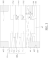
- FIG. 2 is an enlarged view showing an exemplary structure of the via stack VS in the re-distribution structure RDL of FIG. 1 in accordance with an embodiment of the invention, wherein like regions, layers or elements are designated by like numeral numbers or labels.
- the metal stud 102 is landed on an aluminum pad AP of the semiconductor die 100.
- the perimeter of the aluminum pad AP may be covered by a passivation layer 106 such as a silicon nitride layer and a passivation layer 108 such as a polyimide layer.
- An opening OP which has a diameter of about 31 micrometers, for example, is formed in the passivation layer 106 and the passivation layer 108 to expose a central portion of the aluminum pad AP.
- the metal stud 102 is formed in the opening OP and on the passivation layer 108 around the opening OP.
- the width W of the extended portion of the metal stud 102 directly on the passivation layer 108 is about 3 micrometers.
- the height h2 of the metal stud 102 may be, for example, 50 micrometers.
- the via stack VS is composed of a first via V1, a second via V2 stacked on the first via V1, and a third via V3 stacked on the second via V2, which are all substantially aligned with the metal stud 102.
- the first via V1, the second via V2, and the third via V3 may have a diameter of about 31 micrometers, which is equal to the diameter of the opening OP.
- the first via V1 comprises a first flange portion VP1 on the dielectric film PA2
- the second via V2 comprises a second flange portion VP2 on the dielectric film PA3
- the third via V3 comprises a third flange portion VP3 on the dielectric film PA4.
- the first flange portion VP1 may have a width W1 of about 3 micrometers.
- the second flange portion VP2 may have a width W2 of about 3 micrometers.
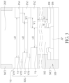
- FIG. 3 is an enlarged view showing an exemplary structure of the via stack VS in the re-distribution structure RDL of FIG. 1 in accordance with another embodiment of the invention, wherein like regions, layers or elements are designated by like numeral numbers or labels.
- the metal stud 102 is landed on an aluminum pad AP of the semiconductor die 100.
- the perimeter of the aluminum pad AP may be covered by a passivation layer 106 and a passivation layer 108 such as a silicon nitride layer.
- An opening OP which has a diameter of about 31 micrometers, for example, is formed in the passivation layer 106 and the passivation layer 108 to expose a central portion of the aluminum pad AP.
- the metal stud 102 is formed in the opening OP and on the passivation layer 108 around the opening OP.
- the width W of the extended portion of the metal stud 102 directly on the passivation layer 108 is about 3 micrometers.
- the height h2 of the metal stud 102 may be, for example, 50 micrometers.
- the via stack VS is composed of a first via V1, a second via V2 stacked on the first via V1, and a third via V3 stacked on the second via V2, which are all substantially aligned with the metal stud 102.
- the first via V1 may have a diameter vd1 of about 31 micrometers, which is equal to the diameter of the opening OP.
- the second via V2 may have a diameter vd2 of about 41 micrometers, which is greater than the diameter of the opening OP.
- the third via V3 may have a diameter vd3 of about 51 micrometers, which is greater than the diameter of the second via V2.
- the first via V1 comprises a first flange portion VP1 on the dielectric film PA2
- the second via V2 comprises a second flange portion VP2 on the dielectric film PA3
- the third via V3 comprises a third flange portion VP3 on the dielectric film PA4.
- the first flange portion VP1 may have a width W1 of about 8 micrometers.
- the second flange portion VP2 may have a width W2 of about 8 micrometers.
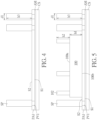
- FIG. 4 to FIG. 14 are schematic, cross-sectional diagrams showing an exemplary method for fabricating a semiconductor package with integrated antenna and shielding pillars in accordance with one embodiment of the invention, wherein like regions, layers or elements are designated by like numeral numbers or labels. It is to be understood that the process steps may be implemented in a wafer-level or panel-level manner.
- a carrier substrate CS having thereon an alignment mark layer AM is provided.
- Abase film PA1 is laminated on the carrier substrate CS.
- the base film PA1 may be a curable polymeric material film such as a polyimide film, but not limited thereto.
- the base film PA1 may have a thickness of about 5-7 micrometers after curing.
- interconnect elements PV1 such as via plugs are formed in the base film PA1 and shielding pillars SP such as copper pillars are formed on the interconnect elements PV1, respectively.
- the shielding pillars SP may have a thickness (or height) h3 of about 80-120 micrometers, for example, 100 micrometers, above a major surface S2 of the base film PA1.
- each of the shielding pillars SP may have a diameter d1 of about 80 micrometers.
- a semiconductor die 100 such as a RFIC die, a base chip, or a 5G wireless chip is then disposed on the major surface S2 of the base film PA1.
- the semiconductor die 100 may have a thickness (or height) h1 of about 40-60 micrometers, for example, 50 micrometers, above the major surface S2 of the base film PA1.
- the semiconductor die 100 has an active surface 100a and a passive, rear surface 100b opposite to the active surface 100a.
- the passive, rear surface 100b is adhered to the base film PA1.
- a plurality of metal studs 102 such as copper studs may be disposed on the active surface 100a of the semiconductor die 100.
- the metal studs 102 may have a thickness (or height) h2 of about 40-60 micrometers, for example, 50 micrometers, above the active surface 100a of the semiconductor die 100.
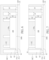
- the semiconductor die 100, the metal studs 102, and the shielding pillars SP are encapsulated by a molding compound MC1.
- the molding compound MC1 is in direct contact with the sidewalls of the semiconductor die 100 and the exposed major surface S2 of the base film PA1.
- a grinding process or a chemical mechanical polishing (CMP) process is then performed to polish the molding compound MC1.
- CMP chemical mechanical polishing
- a re-distribution structure RDL is disposed on the top surface S3 of the molding compound MC1 and is electrically connected to the shielding pillars SP and the metal studs 102.
- the re-distribution structure RDL may comprise dielectric films PA2-PA4 and interconnect structures PV2-PV4 fabricated in or on the dielectric films PA2-PA4, respectively.
- the re-distribution structure RDL may comprise via stacks VS.
- Each of the via stacks VS may be composed of a first via V1, a second via V2 stacked on the first via V1, and a third via V3 stacked on the second via V2, which are all substantially aligned with the corresponding metal stud 102.
- the detailed structure of the via stack VS is illustrated in FIG. 2 and FIG. 3 .
- the dielectric films PA2-PA4 may be curable polymeric material films such as polyimide films, but not limited thereto.
- the interconnect structures PV2-PV4 may comprise conductive traces or conductive vias.
- the dielectric film PA2 may have a thickness of about 5-7 micrometers after curing.
- the dielectric film PA3 may have a thickness of about 5-7 micrometers after curing.
- the dielectric film PA4 may have a thickness of about 5-7 micrometers after curing.
- TMVs through-mold-vias
- the TMVs 202 may comprise an antenna feed line 202f disposed directly on the via stack VS.
- each of the TMVs 202 may have a diameter d2 greater than the diameter d1 of each of the shielding pillars SP.
- each of the TMVs 202 may have a diameter d2 of about 90 micrometers and a height h4 of about 150-200 micrometers.
- the TMVs 202 and the re-distribution structure RDL are encapsulated by a molding compound MC2.
- a molding compound MC2 Preferably, for example, the composition of the molding compound MC2 and the composition of the molding compound MC1 are the same. Alternatively preferably, for example, the composition of the molding compound MC2 may be different from the composition of the molding compound MC1.
- a grinding process or a CMP process is then performed to polish the molding compound MC2.
- the top surfaces of the TMVs 202 are coplanar with a top surface S4 of the molding compound MC2.
- a re-distribution structure RDT is then formed on the top surface S4 of the molding compound MC2 and is electrically connected to the TMVs 202.
- the re-distribution structure RDT may comprise a dielectric film PA5 and an interconnect structure PV5 fabricated in or on the dielectric film PA5.
- the re-distribution structure RDT may comprise an antenna AT on the dielectric film PA5.
- the antenna AT may be electrically connected to the underlying semiconductor die 100 through a via VT, the antenna feed line 202f, the via stack VS and the metal stud 102, which can provide better control for antenna radiation pattern and gain.
- a passivation film PA6 is then formed on the re-distribution structure RDT.
- the passivation film PA6 may be curable polymeric material films such as polyimide films, but not limited thereto.
- the passivation film PA6 may have a thickness of about 5-7 micrometers after curing.
- connection elements BA such as solder balls are formed on the interconnect elements PV1, respectively, for further connection with an application board or a system board (not shown).
- FIG. 15 is a schematic, cross-sectional diagram showing an exemplary semiconductor package with integrated antenna and shielding pillars in accordance with another embodiment of the invention, wherein like regions, layers or elements are designated by like numeral numbers or labels.
- a die 300 is disposed on the re-distribution structure RDL and surrounded by the molding compound MC2.
- the die 300 may be a dummy die, a bridge die, a TSV silicon die, or a flip-chip, but is not limited thereto.
- FIG. 16 is a schematic, cross-sectional diagram showing an exemplary semiconductor package with integrated antenna and shielding pillars in accordance with another embodiment of the invention, wherein like regions, layers or elements are designated by like numeral numbers or labels.
- a die 500 is disposed on the base film PA1 and surrounded by the molding compound MC1.
- the die 500 is coplanar with the semiconductor die 100.
- the die 500 may be a logic die, but is not limited thereto.
Landscapes
- Engineering & Computer Science (AREA)
- Microelectronics & Electronic Packaging (AREA)
- Structures Or Materials For Encapsulating Or Coating Semiconductor Devices Or Solid State Devices (AREA)
- Physics & Mathematics (AREA)
- Encapsulation Of And Coatings For Semiconductor Or Solid State Devices (AREA)
- Semiconductor Integrated Circuits (AREA)
- Geometry (AREA)
- Health & Medical Sciences (AREA)
- Electromagnetism (AREA)
- Toxicology (AREA)
- Moulds For Moulding Plastics Or The Like (AREA)
- Internal Circuitry In Semiconductor Integrated Circuit Devices (AREA)
Abstract
Description
- This application claims the benefit of
U.S. Provisional Application No. 63/289,252, filed on December 14th, 2021 - The present disclosure relates generally to semiconductor packaging. More particularly, the present disclosure relates to an antenna-in-package (AiP) with integrated antenna and shielding pillars.
- With the rising interest in millimeter wave (mmWave) wireless communication systems, such as fifth generation (5G) communication systems, automotive radar, and imaging systems, high gain and high radiation efficiency mmWave antennas have become very important. The mmWave is the frequency band from 30 to 300 GHz and corresponds to wavelengths from 10 mm to 1 mm. In the mmWave band, the antenna is small enough to be efficiently integrated in the package.
- AiP technology is an antenna packaging solution that implements an antenna or antennas in an IC package that can carry a bare RF chip (transceiver). The AiP can be further integrated with front-end components (e.g., power amplifiers (PA) or low-noise amplifiers (LNA)), switches, filters and even power management integrated circuit (PMIC) to form an antenna module using System-in-Package (SiP) technologies.
- A typical FCBGA AiP includes a RF chip (transceiver) attached to a package substrate with solder balls for connection to a main PCB. An array of antennas sits atop the upper portion of the package substrate, allowing wireless communication and detection. Flip-chip techniques are typically utilized to connect the RF chip to the substrate, thereby mitigating the interconnect loss.
- When wireless communication packages with antennas are constructed, package designs need to provide good antenna properties (such as high efficiency, wide bandwidth, etc.) while providing reliable and low cost package solutions.
- One object of the present invention is to provide an improved semiconductor package with integrated antenna and shielding pillars in order to solve the above-mentioned prior art problems or shortcomings. A semiconductor package according to the invention is defined in
independent claim 1. The dependent claims define preferred embodiments thereof. - One aspect of the invention provides a semiconductor package including a base film having a major surface and a bottom surface opposite to the major surface. A semiconductor die is disposed on the major surface of the base film. A plurality of interconnect elements is disposed in the base film and around the semiconductor die. A plurality of metal studs is disposed on an active surface of the semiconductor die. A plurality of shielding pillars is disposed on the interconnect elements of the base film, respectively. A first molding compound encapsulates the semiconductor die, the metal studs, and the shielding pillars on the base film.
- A first re-distribution structure is disposed on a top surface of the first molding compound and is electrically connected to the shielding pillars and the metal studs. The first re-distribution structure includes a via stack electrically connected to and aligned with a corresponding one of the plurality of metal studs. A second molding compound is disposed on the first re-distribution structure. A plurality of through-mold-vias is disposed in the second molding compound. The plurality of through-mold-vias includes an antenna feed line disposed directly on the via stack.
- A second re-distribution structure is disposed on the second molding compound and electrically connected to the through-mold-vias. The second re-distribution structure includes an antenna that is electrically connected to the semiconductor die through the antenna feed line, the via stack, and the corresponding one of the plurality of metal studs. A plurality of connection elements is disposed on the interconnect elements, respectively, on the bottom surface of the base film.
- Preferably, the base film is a curable polymeric material film.
- Preferably, the base film has a thickness of about 5-7 micrometers after curing.
- Preferably, each of the plurality of interconnect elements is exposed from the bottom surface of the base film.
- Preferably, the plurality of interconnect elements comprises solder balls.
- Preferably, the semiconductor die comprises a RFIC die, a base chip, or a 5G wireless chip.
- Preferably, a rear surface of the semiconductor die is adhered to the base film.
- Preferably, the semiconductor die has a first height of about 40-60 micrometers above the major surface of the base film.
- Preferably, the plurality of metal studs has a second height of about 40-60 micrometers.
- Preferably, the plurality of shielding pillars has a third height of about 80-120 micrometers above the major surface of the base film.
- Preferably, the third height is approximately equal to combination of the first height and the second height.
- Preferably, each of the plurality of shielding pillars has a diameter of about 80 micrometers.
- Preferably, top surfaces of the plurality of metal studs and the plurality of shielding pillars are coplanar with the top surface of the first molding compound.
- Preferably, the first re-distribution structure comprises a plurality of dielectric films and a plurality of interconnect structures in or on the plurality of dielectric films.
- Preferably, the plurality of dielectric films comprises curable polymeric material films, and wherein the plurality of interconnect structures comprises conductive traces or conductive vias.
- Preferably, the plurality of interconnect structures further comprises a ground reflector.
- Preferably, each of the plurality of dielectric films has a thickness of about 5-7 micrometers after curing.
- Preferably, the via stack comprises a first via, a second via stacked on the first via, and a third via stacked on the second via, which are all substantially aligned with the corresponding one of the plurality of metal studs.
- Preferably, each of the through-mold-vias has a diameter greater than the diameter of each of the plurality of shielding pillars.
- Preferably, each of the through-mold-vias has a diameter of about 90 micrometers and a height of about 150-200 micrometers.
- Another aspect of the invention provides a semiconductor package including a base film, a semiconductor die disposed on the base film, a plurality of metal studs disposed on an active surface of the semiconductor die, a plurality of shielding pillars disposed on the base film around the semiconductor die, a first molding compound encapsulating the semiconductor die, the metal studs, and the shielding pillars on the base film, a first re-distribution structure disposed on the first molding compound, a second molding compound disposed on the first re-distribution structure, a plurality of through-mold-vias disposed in the second molding compound, and a second re-distribution structure disposed on the second molding compound and electrically connected to the through-mold-vias.
- Preferably, the base film is a curable polymeric material film.
- Preferably, the base film has a thickness of about 5-7 micrometers after curing.
- Preferably, a plurality of interconnect elements is disposed in the base film and around the semiconductor die.
- Preferably, a plurality of connection elements disposed on the interconnect elements, respectively, on a bottom surface of the base film.
- Preferably, the plurality of shielding pillars is disposed on the interconnect elements of the base film, respectively.
- Preferably, the first re-distribution structure is electrically connected to the shielding pillars and the metal studs.
- Preferably, the first re-distribution structure comprises a via stack electrically connected to and aligned with a corresponding one of the plurality of metal studs.
- Preferably, the plurality of through-mold-vias comprises an antenna feed line disposed directly on the via stack.
- Preferably, the second re-distribution structure comprises an antenna that is electrically connected to the semiconductor die through the antenna feed line, the via stack, and the corresponding one of the plurality of metal studs.
- Preferably, each of the through-mold-vias has a diameter greater than the diameter of each of the plurality of shielding pillars.
- Preferably, each of the through-mold-vias has a diameter of about 90 micrometers and a height of about 150-200 micrometers.
- Preferably, a die is disposed in the second molding compound and on the first re-distribution structure.
- Preferably, the die comprises a dummy die, a bridge die, a TSV silicon die, or a flip-chip.
- Preferably, a die is disposed on the base film and is coplanar with the semiconductor die.
- Preferably, the die comprises a logic die.
- These and other objectives of the present invention will no doubt become obvious to those of ordinary skill in the art after reading the following detailed description of the preferred embodiment that is illustrated in the various figures and drawings.
- The accompanying drawings are included to provide a further understanding of the invention and are incorporated in and constitute a part of this specification. The drawings illustrate embodiments of the invention and, together with the description, serve to explain the principles of the invention. In the drawings:
-
FIG. 1 is a schematic, cross-sectional diagram showing an exemplary semiconductor package with integrated antenna and shielding pillars in accordance with one embodiment of the invention; -
FIG. 2 is an enlarged view showing an exemplary structure of the via stack in the re-distribution structure ofFIG. 1 in accordance with an embodiment of the invention; -
FIG. 3 is an enlarged view showing an exemplary structure of the via stack in the re-distribution structure ofFIG. 1 in accordance with another embodiment of the invention; -
FIG. 4 to FIG. 14 are schematic, cross-sectional diagrams showing an exemplary method for fabricating a semiconductor package with integrated antenna and shielding pillars in accordance with one embodiment of the invention; -
FIG. 15 is a schematic, cross-sectional diagram showing an exemplary semiconductor package with integrated antenna and shielding pillars in accordance with another embodiment of the invention; and -
FIG. 16 is a schematic, cross-sectional diagram showing an exemplary semiconductor package with integrated antenna and shielding pillars in accordance with still another embodiment of the invention. - In the following detailed description of embodiments of the invention, reference is made to the accompanying drawings, which form a part hereof, and in which is shown by way of illustration specific preferred embodiments in which the disclosure may be practiced.
- These embodiments are described in sufficient detail to enable those skilled in the art to practice them, and it is to be understood that other embodiments may be utilized and that mechanical, chemical, electrical, and procedural changes may be made without departing from the spirit and scope of the present disclosure. The following detailed description is, therefore, not to be taken in a limiting sense, and the scope of embodiments of the present invention is defined only by the appended claims.
- It will be understood that when an element or layer is referred to as being "on", "connected to" or "coupled to" another element or layer, it can be directly on, connected or coupled to the other element or layer or intervening elements or layers may be present. In contrast, when an element is referred to as being "directly on," "directly connected to" or "directly coupled to" another element or layer, there are no intervening elements or layers present. Like numbers refer to like elements throughout. As used herein, the term "and/or" includes any and all combinations of one or more of the associated listed items.
- The present disclosure pertains to a substrate-less, dual-mold semiconductor package with integrated antenna and shielding pillars. A conventional BT substrate is spared, thereby reducing the dielectric loss and the product cost. The process flexibility is also improved by utilizing dual mold. Preferably, the semiconductor package may be a wafer-level D-band (110-1701GHz) antenna-in-package (AiP) package and may integrate a radio-frequency integrated circuit (RFIC) and one or more than one flipped chips or dies in one package.
- Please refer to
FIG. 1. FIG. 1 is a schematic, cross-sectional diagram showing an exemplary semiconductor package with integrated antenna and shielding pillars in accordance with one embodiment of the invention. As shown inFIG. 1 , asemiconductor die 100 such as a RFIC die, a baseband chip, or a 5G wireless chip is disposed on a surface of a base film PA1. Preferably, the base film PA1 may be a curable polymeric material film such as a polyimide film, but not limited thereto. Preferably, for example, the base film PA1 may have a thickness of about 5-7 micrometers after curing. - Preferably, interconnect elements PV1 such as via plugs are disposed in the base film PA1 around the semiconductor die 100. Preferably, for example, each of the interconnect elements PV1 may have a barrier layer BL such as titanium or titanium nitride, and a low-resistance metal LC such as copper. The barrier layer BL of each of the interconnect elements PV1 may be exposed from a bottom surface S1 of the base film PA1. Preferably, connection elements BA such as solder balls may be disposed on the interconnect elements PV1, respectively, for further connection with an application board or a system board (not shown).
- Preferably, the semiconductor die 100 may have a thickness (or height) h1 of about 40-60 micrometers, for example, 50 micrometers, above a major surface S2 of the base film PA1. Preferably, the semiconductor die 100 has an
active surface 100a and a passive,rear surface 100b opposite to theactive surface 100a. Preferably, the passive,rear surface 100b is adhered to the base film PA1. Preferably, a plurality of input/output (I/O)pads 101 may be disposed on theactive surface 100a of the semiconductor die 100. - Preferably, a plurality of
metal studs 102 such as copper studs may be disposed on the plurality of I/O pads 101, respectively. Preferably, themetal studs 102 may have a thickness (or height) h2 of about 40-60 micrometers, for example, 50 micrometers, above theactive surface 100a of the semiconductor die 100. - Preferably, shielding pillars SP such as copper pillars are disposed on the interconnect elements PV1 of the base film PA1, respectively. Preferably, the shielding pillars SP may have a thickness (or height) h3 of about 80-120 micrometers, for example, 100 micrometers, above a major surface S2 of the base film PA1. Preferably, for example, each of the shielding pillars SP may have a diameter d1 of about 80 micrometers. Preferably, the height h3 may be approximately equal to the combination of the height h1 and the height h2. Preferably, the semiconductor die 100, the
metal studs 102, and the shielding pillars SP are encapsulated by a molding compound MC1. The molding compound MC1 is in direct contact with the sidewalls of the semiconductor die 100. Preferably, the top surfaces of themetal studs 102 and the shielding pillars SP are coplanar with a top surface S3 of the molding compound MC1. - Preferably, a re-distribution structure RDL is disposed on the top surface S3 of the molding compound MC1 and is electrically connected to the shielding pillars SP and the
metal studs 102. Preferably, for example, the re-distribution structure RDL may comprise dielectric films PA2-PA4 and interconnect structures PV2-PV4 fabricated in or on the dielectric films PA2-PA4, respectively. Preferably, the re-distribution structure RDL may comprise via stacks VS. Each of the via stacks VS may be composed of a first via V1, a second via V2 stacked on the first via V1, and a third via V3 stacked on the second via V2, which are all substantially aligned with the correspondingmetal stud 102. Preferably, the first via V1 comprises a first flange portion VP1 on the dielectric film PA2, the second via V2 comprises a second flange portion VP2 on the dielectric film PA3, and the third via V3 comprises a third flange portion VP3 on the dielectric film PA4. - Preferably, for example, the dielectric films PA2-PA4 may be curable polymeric material films such as polyimide films, but not limited thereto. Preferably, for example, the interconnect structures PV2-PV4 may comprise conductive traces or conductive vias. Preferably, for example, the interconnect structure PV4 may comprise a ground reflector GR. Preferably, for example, the dielectric film PA2 may have a thickness of about 5-7 micrometers after curing. Preferably, for example, the dielectric film PA3 may have a thickness of about 5-7 micrometers after curing. Preferably, for example, the dielectric film PA4 may have a thickness of about 5-7 micrometers after curing.
- Preferably, the re-distribution structure RDL is encapsulated by a molding compound MC2. For example, the molding compound MC2 may have a thickness of about 150-200 micrometers. A plurality of through-mold-vias (TMVs) 202 is disposed in the molding compound MC2. The
TMVs 202 may comprise anantenna feed line 202f disposed directly on the via stack VS. Preferably, each of theTMVs 202 may have a diameter d2 greater than the diameter d1 of each of the shielding pillars SP. Preferably, for example, each of theTMVs 202 may have a diameter d2 of about 90 micrometers and a height h4 of about 150-200 micrometers. Preferably, the top surfaces of theTMVs 202 are coplanar with the top surface S4 of the molding compound MC2. - Preferably, a re-distribution structure RDT is disposed on the top surface S4 of the molding compound MC2 and is electrically connected to the
TMVs 202. Preferably, for example, the re-distribution structure RDT may comprise a dielectric film PA5 and an interconnect structure PV5 fabricated in or on the dielectric film PA5. Preferably, the re-distribution structure RDT may comprise an antenna AT on the dielectric film PA5. The antenna AT may be electrically connected to the underlying semiconductor die 100 through a via VT, theantenna feed line 202f, the via stack VS and themetal stud 102, which can provide better control for antenna radiation pattern and gain. The distance between the ground reflector GR and the antenna AT may be adjusted by controlling the thickness of the molding compound MC2. - Preferably, for example, the dielectric film PA5 may be curable polymeric material films such as polyimide films, but not limited thereto. Preferably, for example, the interconnect structure PV5 may comprise conductive traces or conductive vias. Preferably, for example, the dielectric film PA5 may have a thickness of about 5-7 micrometers after curing. A passivation film PA6 may be disposed on the re-distribution structure RDT. The passivation film PA6 may be curable polymeric material films such as polyimide films, but not limited thereto. Preferably, for example, the passivation film PA6 may have a thickness of about 5-7 micrometers after curing.
-
FIG. 2 is an enlarged view showing an exemplary structure of the via stack VS in the re-distribution structure RDL ofFIG. 1 in accordance with an embodiment of the invention, wherein like regions, layers or elements are designated by like numeral numbers or labels. As shown inFIG. 2 , themetal stud 102 is landed on an aluminum pad AP of the semiconductor die 100. The perimeter of the aluminum pad AP may be covered by apassivation layer 106 such as a silicon nitride layer and apassivation layer 108 such as a polyimide layer. An opening OP, which has a diameter of about 31 micrometers, for example, is formed in thepassivation layer 106 and thepassivation layer 108 to expose a central portion of the aluminum pad AP. Themetal stud 102 is formed in the opening OP and on thepassivation layer 108 around the opening OP. For example, the width W of the extended portion of themetal stud 102 directly on thepassivation layer 108 is about 3 micrometers. The height h2 of themetal stud 102 may be, for example, 50 micrometers. - Preferably, the via stack VS is composed of a first via V1, a second via V2 stacked on the first via V1, and a third via V3 stacked on the second via V2, which are all substantially aligned with the
metal stud 102. Preferably, for example, the first via V1, the second via V2, and the third via V3 may have a diameter of about 31 micrometers, which is equal to the diameter of the opening OP. Preferably, the first via V1 comprises a first flange portion VP1 on the dielectric film PA2, the second via V2 comprises a second flange portion VP2 on the dielectric film PA3, and the third via V3 comprises a third flange portion VP3 on the dielectric film PA4. Preferably, for example, the first flange portion VP1 may have a width W1 of about 3 micrometers. Preferably, for example, the second flange portion VP2 may have a width W2 of about 3 micrometers. -
FIG. 3 is an enlarged view showing an exemplary structure of the via stack VS in the re-distribution structure RDL ofFIG. 1 in accordance with another embodiment of the invention, wherein like regions, layers or elements are designated by like numeral numbers or labels. As shown inFIG. 3 , likewise, themetal stud 102 is landed on an aluminum pad AP of the semiconductor die 100. The perimeter of the aluminum pad AP may be covered by apassivation layer 106 and apassivation layer 108 such as a silicon nitride layer. An opening OP, which has a diameter of about 31 micrometers, for example, is formed in thepassivation layer 106 and thepassivation layer 108 to expose a central portion of the aluminum pad AP. Themetal stud 102 is formed in the opening OP and on thepassivation layer 108 around the opening OP. For example, the width W of the extended portion of themetal stud 102 directly on thepassivation layer 108 is about 3 micrometers. The height h2 of themetal stud 102 may be, for example, 50 micrometers. - Preferably, the via stack VS is composed of a first via V1, a second via V2 stacked on the first via V1, and a third via V3 stacked on the second via V2, which are all substantially aligned with the
metal stud 102. Preferably, for example, the first via V1 may have a diameter vd1 of about 31 micrometers, which is equal to the diameter of the opening OP. The second via V2 may have a diameter vd2 of about 41 micrometers, which is greater than the diameter of the opening OP. The third via V3 may have a diameter vd3 of about 51 micrometers, which is greater than the diameter of the second via V2. Preferably, likewise, the first via V1 comprises a first flange portion VP1 on the dielectric film PA2, the second via V2 comprises a second flange portion VP2 on the dielectric film PA3, and the third via V3 comprises a third flange portion VP3 on the dielectric film PA4. Preferably, for example, the first flange portion VP1 may have a width W1 of about 8 micrometers. Preferably, for example, the second flange portion VP2 may have a width W2 of about 8 micrometers. When viewed from the above, themetal stud 102 is completely overlapped with the first via V1, and the first via V1 is completely overlapped with the second via V2. -
FIG. 4 to FIG. 14 are schematic, cross-sectional diagrams showing an exemplary method for fabricating a semiconductor package with integrated antenna and shielding pillars in accordance with one embodiment of the invention, wherein like regions, layers or elements are designated by like numeral numbers or labels. It is to be understood that the process steps may be implemented in a wafer-level or panel-level manner. - As shown in
FIG. 4 , a carrier substrate CS having thereon an alignment mark layer AM is provided. Abase film PA1 is laminated on the carrier substrate CS. Preferably, the base film PA1 may be a curable polymeric material film such as a polyimide film, but not limited thereto. Preferably, for example, the base film PA1 may have a thickness of about 5-7 micrometers after curing. - Subsequently, interconnect elements PV1 such as via plugs are formed in the base film PA1 and shielding pillars SP such as copper pillars are formed on the interconnect elements PV1, respectively. Preferably, the shielding pillars SP may have a thickness (or height) h3 of about 80-120 micrometers, for example, 100 micrometers, above a major surface S2 of the base film PA1. Preferably, for example, each of the shielding pillars SP may have a diameter d1 of about 80 micrometers.
- As shown in
FIG. 5 , asemiconductor die 100 such as a RFIC die, a base chip, or a 5G wireless chip is then disposed on the major surface S2 of the base film PA1. Preferably, the semiconductor die 100 may have a thickness (or height) h1 of about 40-60 micrometers, for example, 50 micrometers, above the major surface S2 of the base film PA1. Preferably, the semiconductor die 100 has anactive surface 100a and a passive,rear surface 100b opposite to theactive surface 100a. Preferably, the passive,rear surface 100b is adhered to the base film PA1. - Preferably, a plurality of
metal studs 102 such as copper studs may be disposed on theactive surface 100a of the semiconductor die 100. Preferably, themetal studs 102 may have a thickness (or height) h2 of about 40-60 micrometers, for example, 50 micrometers, above theactive surface 100a of the semiconductor die 100. - As shown in
FIG. 6 , subsequently, the semiconductor die 100, themetal studs 102, and the shielding pillars SP are encapsulated by a molding compound MC1. The molding compound MC1 is in direct contact with the sidewalls of the semiconductor die 100 and the exposed major surface S2 of the base film PA1. - As shown in
FIG. 7 , a grinding process or a chemical mechanical polishing (CMP) process is then performed to polish the molding compound MC1. After the CMP process, the top surfaces of themetal studs 102 and the shielding pillars SP are coplanar with a top surface S3 of the molding compound MC1. - As shown in
FIG. 8 , a re-distribution structure RDL is disposed on the top surface S3 of the molding compound MC1 and is electrically connected to the shielding pillars SP and themetal studs 102. Preferably, for example, the re-distribution structure RDL may comprise dielectric films PA2-PA4 and interconnect structures PV2-PV4 fabricated in or on the dielectric films PA2-PA4, respectively. Preferably, the re-distribution structure RDL may comprise via stacks VS. Each of the via stacks VS may be composed of a first via V1, a second via V2 stacked on the first via V1, and a third via V3 stacked on the second via V2, which are all substantially aligned with the correspondingmetal stud 102. The detailed structure of the via stack VS is illustrated inFIG. 2 andFIG. 3 . - Preferably, for example, the dielectric films PA2-PA4 may be curable polymeric material films such as polyimide films, but not limited thereto. Preferably, for example, the interconnect structures PV2-PV4 may comprise conductive traces or conductive vias. Preferably, for example, the dielectric film PA2 may have a thickness of about 5-7 micrometers after curing. Preferably, for example, the dielectric film PA3 may have a thickness of about 5-7 micrometers after curing. Preferably, for example, the dielectric film PA4 may have a thickness of about 5-7 micrometers after curing.
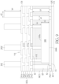
- As shown in
FIG. 9 , through-mold-vias (TMVs) 202 are formed on the re-distribution structure RDL. TheTMVs 202 may comprise anantenna feed line 202f disposed directly on the via stack VS. Preferably, each of theTMVs 202 may have a diameter d2 greater than the diameter d1 of each of the shielding pillars SP. Preferably, for example, each of theTMVs 202 may have a diameter d2 of about 90 micrometers and a height h4 of about 150-200 micrometers. - As shown in
FIG. 10 , subsequently, theTMVs 202 and the re-distribution structure RDL are encapsulated by a molding compound MC2. Preferably, for example, the composition of the molding compound MC2 and the composition of the molding compound MC1 are the same. Alternatively preferably, for example, the composition of the molding compound MC2 may be different from the composition of the molding compound MC1. - As shown in
FIG. 11 , a grinding process or a CMP process is then performed to polish the molding compound MC2. After the CMP process, the top surfaces of theTMVs 202 are coplanar with a top surface S4 of the molding compound MC2. - As shown in
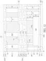
FIG. 12 , a re-distribution structure RDT is then formed on the top surface S4 of the molding compound MC2 and is electrically connected to theTMVs 202. Preferably, for example, the re-distribution structure RDT may comprise a dielectric film PA5 and an interconnect structure PV5 fabricated in or on the dielectric film PA5. Preferably, the re-distribution structure RDT may comprise an antenna AT on the dielectric film PA5. The antenna AT may be electrically connected to the underlying semiconductor die 100 through a via VT, theantenna feed line 202f, the via stack VS and themetal stud 102, which can provide better control for antenna radiation pattern and gain. - As shown in
FIG. 13 , a passivation film PA6 is then formed on the re-distribution structure RDT. Preferably, the passivation film PA6 may be curable polymeric material films such as polyimide films, but not limited thereto. Preferably, for example, the passivation film PA6 may have a thickness of about 5-7 micrometers after curing. - As shown in
FIG. 14 , after the formation of the passivation film PA6, the carrier substrate CS is removed. Preferably, connection elements BA such as solder balls are formed on the interconnect elements PV1, respectively, for further connection with an application board or a system board (not shown). -
FIG. 15 is a schematic, cross-sectional diagram showing an exemplary semiconductor package with integrated antenna and shielding pillars in accordance with another embodiment of the invention, wherein like regions, layers or elements are designated by like numeral numbers or labels. As shown inFIG. 15 , adie 300 is disposed on the re-distribution structure RDL and surrounded by the molding compound MC2. Preferably, thedie 300 may be a dummy die, a bridge die, a TSV silicon die, or a flip-chip, but is not limited thereto. -
FIG. 16 is a schematic, cross-sectional diagram showing an exemplary semiconductor package with integrated antenna and shielding pillars in accordance with another embodiment of the invention, wherein like regions, layers or elements are designated by like numeral numbers or labels. As shown inFIG. 16 , adie 500 is disposed on the base film PA1 and surrounded by the molding compound MC1. Thedie 500 is coplanar with the semiconductor die 100. Preferably, for example, thedie 500 may be a logic die, but is not limited thereto. - Those skilled in the art will readily observe that numerous modifications and alterations of the device and method may be made while retaining the teachings of the invention. Accordingly, the above disclosure should be construed as limited only by the metes and bounds of the appended claims.
Claims (15)
- A semiconductor package (1), comprising:a base film (PA1);a semiconductor die (100) disposed on the base film (PA1);a plurality of metal studs (102) disposed on an active surface (100a) of the semiconductor die (100);a plurality of shielding pillars (SP) disposed on the base film (PA1);a first molding compound (MC1) encapsulating the semiconductor die (100), the metal studs (102), and the shielding pillars (SP) on the base film (PA1);a first re-distribution structure (RDL) disposed on the first molding compound (MC1);a second molding compound (MC2) disposed on the first re-distribution structure (RDL);a plurality of through-mold-vias (202 disposed in the second molding compound (MC2); anda second re-distribution structure (RDT) disposed on the second molding compound (MC2) and electrically connected to the through-mold-vias (202).
- The semiconductor package (1) according to claim 1, wherein the base film (PA1) is a curable polymeric material film; and/or
wherein the base film has a thickness of about 5-7 micrometers after curing. - The semiconductor package (1) according to claim 1 or 2, wherein a plurality of interconnect elements (PV1) is disposed in the base film (PA1) and around the semiconductor die (100).
- The semiconductor package (1) according to claim 3, further comprising a plurality of connection elements (BA) disposed on the interconnect elements (PV1), respectively, on a bottom surface (S1) of the base film (PA1); and/or
wherein the plurality of shielding pillars (SP) is disposed on the interconnect elements (PV1) of the base film (PA1), respectively. - The semiconductor package (1) according to any one of claims 1 to 4, wherein the first re-distribution structure (RDL) is electrically connected to the shielding pillars (SP) and the metal studs (102); and/orwherein the first re-distribution structure (PDL) comprises a via stack (VS) electrically connected to and aligned with a corresponding one of the plurality of metal studs (102),wherein preferably the plurality of through-mold-vias (202) comprises an antenna feed line (202f) disposed directly on the via stack (VS),wherein further preferably the second re-distribution structure (RDT) comprises an antenna (AT) that is electrically connected to the semiconductor die (100) through the antenna feed line (202f), the via stack (VS), and the corresponding one of the plurality of metal studs (102).
- The semiconductor package (1) according to any one of claims 1 to 5, whereinthe base film (PA1) has a major surface (S2) and a bottom surface (S1) opposite to the major surface (S2);the semiconductor die (100) is disposed on the major surface (S2) of the base film (PA1); andthe first re-distribution structure (RDL) is disposed on a top surface (S3) of the first molding compound.
- The semiconductor package (1) according to any one of claims 1 to 6, wherein each of the plurality of interconnect elements (PV1) is exposed from the bottom surface (S1) of the base film (PA1); and/or
wherein the plurality of interconnect elements (PV1) comprises solder balls (BA). - The semiconductor package (1) according to any one of claims 1 to 7, wherein the semiconductor die (100) comprises a RFIC die, a baseband chip, or a 5G wireless chip; and/or wherein a rear surface (100b) of the semiconductor die (100) is adhered to the base film (PA1).
- The semiconductor package (1) according to any one of claims 1 to 8, wherein the semiconductor die (100) has a first height (h1) of about 40-60 micrometers above the major surface (S2) of the base film (PA1);wherein preferably the plurality of metal studs (102) has a second height (h2) of about 40-60 micrometers;wherein further preferably the plurality of shielding pillars (SP) has a third height (h3) of about 80-120 micrometers above the major surface (S2) of the base film (PA1);wherein still further preferably the third height (h3) is approximately equal to combination of the first height (h1) and the second height (h2).
- The semiconductor package (1) according to any one of claims 1 to 9, wherein each of the plurality of shielding pillars (SP) has a diameter (d1) of about 80 micrometers; and/orwherein each of the through-mold-vias (202) has a diameter (d2) greater than the diameter (d1) of each of the plurality of shielding pillars (SP); and/orwherein each of the through-mold-vias (202) has a diameter (d2) of about 90 micrometers and a height (h4) of about 150-200 micrometers.
- The semiconductor package (1) according to any one of claims 1 to 10, wherein top surfaces of the plurality of metal studs (102) and the plurality of shielding pillars (SP) are coplanar with the top surface (S3) of the first molding compound (MC1).
- The semiconductor (1) package according to any one of claims 1 to 11, wherein the first re-distribution structure (RDL) comprises a plurality of dielectric films (PA2-PA4) and a plurality of interconnect structures (PV2-PV4) in or on the plurality of dielectric films (PA2-PA4).
- The semiconductor package (1) according to claim 12, wherein the plurality of dielectric films (PA2-PA4) comprises curable polymeric material films, and wherein the plurality of interconnect structures (PV2-PV4) comprises conductive traces or conductive vias; and/orwherein the plurality of interconnect structures (PV2-PV4) further comprises a ground reflector (GR); and/orwherein each of the plurality of dielectric films (PA2-PA4) has a thickness of about 5-7 micrometers after curing.
- The semiconductor package (1) according to any one of claims 1 to 13, wherein the via stack (VS) comprises a first via (V1), a second via (V2) stacked on the first via (V1), and a third via (V3) stacked on the second via (V2), which are all substantially aligned with the corresponding one of the plurality of metal studs (102).
- The semiconductor package (1) according to any one of claims 1 to 14, wherein a die (300) is disposed in the second molding compound (MC2) and on the first re-distribution structure (RDL),wherein preferably the die (300) comprises a dummy die, a bridge die, a TSV silicon die, or a flip-chip; and/orwherein a die (500) is disposed on the base film (PA1) and is coplanar with the semiconductor die (100),wherein preferably the die (500) comprises a logic die.
Applications Claiming Priority (2)
| Application Number | Priority Date | Filing Date | Title |
|---|---|---|---|
| US202163289252P | 2021-12-14 | 2021-12-14 | |
| US17/987,873 US12500180B2 (en) | 2021-12-14 | 2022-11-16 | Semiconductor package with integrated antenna and shielding pillars |
Publications (2)
| Publication Number | Publication Date |
|---|---|
| EP4210166A2 true EP4210166A2 (en) | 2023-07-12 |
| EP4210166A3 EP4210166A3 (en) | 2023-09-06 |
Family
ID=84440059
Family Applications (1)
| Application Number | Title | Priority Date | Filing Date |
|---|---|---|---|
| EP22211882.0A Pending EP4210166A3 (en) | 2021-12-14 | 2022-12-07 | Semiconductor package with integrated antenna and shielding pillars |
Country Status (4)
| Country | Link |
|---|---|
| US (1) | US12500180B2 (en) |
| EP (1) | EP4210166A3 (en) |
| CN (1) | CN116435265A (en) |
| TW (1) | TWI854381B (en) |
Families Citing this family (3)
| Publication number | Priority date | Publication date | Assignee | Title |
|---|---|---|---|---|
| US20230268355A1 (en) * | 2022-02-23 | 2023-08-24 | Taiwan Semiconductor Manufacturing Company, Ltd. | Integrated circuit device and method for fabricating the same |
| CN116826368A (en) * | 2023-07-25 | 2023-09-29 | 加特兰微电子科技(上海)有限公司 | An antenna system, radar sensor system and electronic device |
| US20250157953A1 (en) * | 2023-11-14 | 2025-05-15 | Ap Memory Technology Corporation | Vertical semiconductor rfid structure, rfid tag device, and manufacturing method thereof |
Family Cites Families (17)
| Publication number | Priority date | Publication date | Assignee | Title |
|---|---|---|---|---|
| US7486525B2 (en) * | 2006-08-04 | 2009-02-03 | International Business Machines Corporation | Temporary chip attach carrier |
| DE102016110862B4 (en) | 2016-06-14 | 2022-06-30 | Snaptrack, Inc. | Module and method of making a variety of modules |
| US10103125B2 (en) | 2016-11-28 | 2018-10-16 | Taiwan Semiconductor Manufacturing Co., Ltd. | Chip package structure and method for forming the same |
| US10134683B2 (en) | 2017-02-10 | 2018-11-20 | Advanced Semiconductor Engineering, Inc. | Semiconductor device package and method of manufacturing the same |
| US10354964B2 (en) | 2017-02-24 | 2019-07-16 | Taiwan Semiconductor Manufacturing Company, Ltd. | Integrated devices in semiconductor packages and methods of forming same |
| US10483617B2 (en) | 2017-09-29 | 2019-11-19 | Taiwan Semiconductor Manufacturing Co., Ltd. | Package structure |
| US10763206B2 (en) | 2017-10-30 | 2020-09-01 | Taiwan Semiconductor Manufacturing Co., Ltd. | Method of fabricating integrated fan-out packages |
| US10424550B2 (en) | 2017-12-19 | 2019-09-24 | National Chung Shan Institute Of Science And Technology | Multi-band antenna package structure, manufacturing method thereof and communication device |
| US11270953B2 (en) | 2018-08-31 | 2022-03-08 | Taiwan Semiconductor Manufacturing Co., Ltd. | Structure and formation method of chip package with shielding structure |
| IT201900006736A1 (en) | 2019-05-10 | 2020-11-10 | Applied Materials Inc | PACKAGE MANUFACTURING PROCEDURES |
| US10777518B1 (en) | 2019-05-16 | 2020-09-15 | Taiwan Semiconductor Manufacturing Co., Ltd. | Package structure and method of manufacturing the same |
| EP3745457B1 (en) | 2019-05-28 | 2024-12-04 | Mediatek Inc. | Semiconductor package having discrete antenna device |
| US11018083B2 (en) | 2019-07-17 | 2021-05-25 | Taiwan Semiconductor Manufacturing Company, Ltd. | Semiconductor package and manufacturing method thereof |
| KR102674087B1 (en) | 2019-09-06 | 2024-06-12 | 에스케이하이닉스 주식회사 | Semiconductor package including electromagnetic interference shielding layer |
| TWI768294B (en) | 2019-12-31 | 2022-06-21 | 力成科技股份有限公司 | Package structure and manufacturing method thereof |
| US12113022B2 (en) * | 2020-05-26 | 2024-10-08 | Taiwan Semiconductor Manufacturing Company, Ltd. | Semiconductor package and manufacturing method of semiconductor package |
| US11430776B2 (en) | 2020-06-15 | 2022-08-30 | Taiwan Semiconductor Manufacturing Co., Ltd. | Semiconductor devices and methods of manufacturing |
-
2022
- 2022-11-16 US US17/987,873 patent/US12500180B2/en active Active
- 2022-11-28 TW TW111145366A patent/TWI854381B/en active
- 2022-11-28 CN CN202211500757.8A patent/CN116435265A/en active Pending
- 2022-12-07 EP EP22211882.0A patent/EP4210166A3/en active Pending
Also Published As
| Publication number | Publication date |
|---|---|
| US12500180B2 (en) | 2025-12-16 |
| US20230187377A1 (en) | 2023-06-15 |
| TWI854381B (en) | 2024-09-01 |
| CN116435265A (en) | 2023-07-14 |
| TW202324651A (en) | 2023-06-16 |
| EP4210166A3 (en) | 2023-09-06 |
Similar Documents
| Publication | Publication Date | Title |
|---|---|---|
| US12588222B2 (en) | Semiconductor package including an integrated circuit die and an inductor or a transformer | |
| US11996372B2 (en) | Semiconductor device and method of manufacture | |
| US10566299B2 (en) | Method for manufacturing a multi-band antenna package structure | |
| US20250309032A1 (en) | Heat dissipation structures for integrated circuit packages and methods of forming the same | |
| EP3413347B1 (en) | Semiconductor package having discrete antenna device | |
| US12500180B2 (en) | Semiconductor package with integrated antenna and shielding pillars | |
| US12593699B2 (en) | Package structure | |
| US12068302B2 (en) | Semiconductor package | |
| US12033963B2 (en) | Package structure comprising thermally conductive layer around the IC die | |
| US10128192B2 (en) | Fan-out package structure | |
| US12057415B2 (en) | Semiconductor device having antenna and manufacturing method thereof | |
| US20200020643A1 (en) | Semicondcutor packages with electromagnetic interference shielding layer and methods of forming the same | |
| KR20220150201A (en) | Semiconductor package with riveting structure between two rings and method for forming the same | |
| US12125766B2 (en) | Thermoelectric cooling packages | |
| US20250364451A1 (en) | Semiconductor device and method of manufacture | |
| CN117174669A (en) | Electronic packages and manufacturing methods | |
| US20250293424A1 (en) | Electronic package and manufacturing method thereof |
Legal Events
| Date | Code | Title | Description |
|---|---|---|---|
| PUAI | Public reference made under article 153(3) epc to a published international application that has entered the european phase |
Free format text: ORIGINAL CODE: 0009012 |
|
| STAA | Information on the status of an ep patent application or granted ep patent |
Free format text: STATUS: THE APPLICATION HAS BEEN PUBLISHED |
|
| AK | Designated contracting states |
Kind code of ref document: A2 Designated state(s): AL AT BE BG CH CY CZ DE DK EE ES FI FR GB GR HR HU IE IS IT LI LT LU LV MC ME MK MT NL NO PL PT RO RS SE SI SK SM TR |
|
| PUAL | Search report despatched |
Free format text: ORIGINAL CODE: 0009013 |
|
| AK | Designated contracting states |
Kind code of ref document: A3 Designated state(s): AL AT BE BG CH CY CZ DE DK EE ES FI FR GB GR HR HU IE IS IT LI LT LU LV MC ME MK MT NL NO PL PT RO RS SE SI SK SM TR |
|
| RIC1 | Information provided on ipc code assigned before grant |
Ipc: H01L 23/498 20060101ALN20230801BHEP Ipc: H01L 25/065 20230101ALN20230801BHEP Ipc: H01L 23/538 20060101ALN20230801BHEP Ipc: H01L 23/00 20060101ALI20230801BHEP Ipc: H01L 23/66 20060101ALI20230801BHEP Ipc: H01L 23/552 20060101ALI20230801BHEP Ipc: H01Q 1/22 20060101AFI20230801BHEP |
|
| STAA | Information on the status of an ep patent application or granted ep patent |
Free format text: STATUS: REQUEST FOR EXAMINATION WAS MADE |
|
| 17P | Request for examination filed |
Effective date: 20240305 |
|
| RBV | Designated contracting states (corrected) |
Designated state(s): AL AT BE BG CH CY CZ DE DK EE ES FI FR GB GR HR HU IE IS IT LI LT LU LV MC ME MK MT NL NO PL PT RO RS SE SI SK SM TR |