EP4210115A1 - Diode with contact structure including an improved barrier region and related manufacturing process - Google Patents
Diode with contact structure including an improved barrier region and related manufacturing process Download PDFInfo
- Publication number
- EP4210115A1 EP4210115A1 EP22212787.0A EP22212787A EP4210115A1 EP 4210115 A1 EP4210115 A1 EP 4210115A1 EP 22212787 A EP22212787 A EP 22212787A EP 4210115 A1 EP4210115 A1 EP 4210115A1
- Authority
- EP
- European Patent Office
- Prior art keywords
- region
- forming
- anode region
- main anode
- barrier
- Prior art date
- Legal status (The legal status is an assumption and is not a legal conclusion. Google has not performed a legal analysis and makes no representation as to the accuracy of the status listed.)
- Pending
Links
Images










Classifications
-
- H—ELECTRICITY
- H10—SEMICONDUCTOR DEVICES; ELECTRIC SOLID-STATE DEVICES NOT OTHERWISE PROVIDED FOR
- H10D—INORGANIC ELECTRIC SEMICONDUCTOR DEVICES
- H10D64/00—Electrodes of devices having potential barriers
- H10D64/60—Electrodes characterised by their materials
- H10D64/64—Electrodes comprising a Schottky barrier to a semiconductor
-
- H—ELECTRICITY
- H10—SEMICONDUCTOR DEVICES; ELECTRIC SOLID-STATE DEVICES NOT OTHERWISE PROVIDED FOR
- H10D—INORGANIC ELECTRIC SEMICONDUCTOR DEVICES
- H10D8/00—Diodes
- H10D8/411—PN diodes having planar bodies
-
- H—ELECTRICITY
- H10—SEMICONDUCTOR DEVICES; ELECTRIC SOLID-STATE DEVICES NOT OTHERWISE PROVIDED FOR
- H10D—INORGANIC ELECTRIC SEMICONDUCTOR DEVICES
- H10D62/00—Semiconductor bodies, or regions thereof, of devices having potential barriers
- H10D62/10—Shapes, relative sizes or dispositions of the regions of the semiconductor bodies; Shapes of the semiconductor bodies
- H10D62/102—Constructional design considerations for preventing surface leakage or controlling electric field concentration
- H10D62/103—Constructional design considerations for preventing surface leakage or controlling electric field concentration for increasing or controlling the breakdown voltage of reverse-biased devices
- H10D62/105—Constructional design considerations for preventing surface leakage or controlling electric field concentration for increasing or controlling the breakdown voltage of reverse-biased devices by having particular doping profiles, shapes or arrangements of PN junctions; by having supplementary regions, e.g. junction termination extension [JTE]
- H10D62/106—Constructional design considerations for preventing surface leakage or controlling electric field concentration for increasing or controlling the breakdown voltage of reverse-biased devices by having particular doping profiles, shapes or arrangements of PN junctions; by having supplementary regions, e.g. junction termination extension [JTE] having supplementary regions doped oppositely to or in rectifying contact with regions of the semiconductor bodies, e.g. guard rings with PN or Schottky junctions
-
- H—ELECTRICITY
- H10—SEMICONDUCTOR DEVICES; ELECTRIC SOLID-STATE DEVICES NOT OTHERWISE PROVIDED FOR
- H10D—INORGANIC ELECTRIC SEMICONDUCTOR DEVICES
- H10D62/00—Semiconductor bodies, or regions thereof, of devices having potential barriers
- H10D62/10—Shapes, relative sizes or dispositions of the regions of the semiconductor bodies; Shapes of the semiconductor bodies
- H10D62/102—Constructional design considerations for preventing surface leakage or controlling electric field concentration
- H10D62/103—Constructional design considerations for preventing surface leakage or controlling electric field concentration for increasing or controlling the breakdown voltage of reverse-biased devices
- H10D62/105—Constructional design considerations for preventing surface leakage or controlling electric field concentration for increasing or controlling the breakdown voltage of reverse-biased devices by having particular doping profiles, shapes or arrangements of PN junctions; by having supplementary regions, e.g. junction termination extension [JTE]
- H10D62/106—Constructional design considerations for preventing surface leakage or controlling electric field concentration for increasing or controlling the breakdown voltage of reverse-biased devices by having particular doping profiles, shapes or arrangements of PN junctions; by having supplementary regions, e.g. junction termination extension [JTE] having supplementary regions doped oppositely to or in rectifying contact with regions of the semiconductor bodies, e.g. guard rings with PN or Schottky junctions
- H10D62/107—Buried supplementary regions, e.g. buried guard rings
-
- H—ELECTRICITY
- H10—SEMICONDUCTOR DEVICES; ELECTRIC SOLID-STATE DEVICES NOT OTHERWISE PROVIDED FOR
- H10D—INORGANIC ELECTRIC SEMICONDUCTOR DEVICES
- H10D62/00—Semiconductor bodies, or regions thereof, of devices having potential barriers
- H10D62/10—Shapes, relative sizes or dispositions of the regions of the semiconductor bodies; Shapes of the semiconductor bodies
- H10D62/128—Anode regions of diodes
-
- H—ELECTRICITY
- H10—SEMICONDUCTOR DEVICES; ELECTRIC SOLID-STATE DEVICES NOT OTHERWISE PROVIDED FOR
- H10D—INORGANIC ELECTRIC SEMICONDUCTOR DEVICES
- H10D62/00—Semiconductor bodies, or regions thereof, of devices having potential barriers
- H10D62/10—Shapes, relative sizes or dispositions of the regions of the semiconductor bodies; Shapes of the semiconductor bodies
- H10D62/13—Semiconductor regions connected to electrodes carrying current to be rectified, amplified or switched, e.g. source or drain regions
-
- H—ELECTRICITY
- H10—SEMICONDUCTOR DEVICES; ELECTRIC SOLID-STATE DEVICES NOT OTHERWISE PROVIDED FOR
- H10D—INORGANIC ELECTRIC SEMICONDUCTOR DEVICES
- H10D62/00—Semiconductor bodies, or regions thereof, of devices having potential barriers
- H10D62/80—Semiconductor bodies, or regions thereof, of devices having potential barriers characterised by the materials
- H10D62/83—Semiconductor bodies, or regions thereof, of devices having potential barriers characterised by the materials being Group IV materials, e.g. B-doped Si or undoped Ge
-
- H—ELECTRICITY
- H10—SEMICONDUCTOR DEVICES; ELECTRIC SOLID-STATE DEVICES NOT OTHERWISE PROVIDED FOR
- H10D—INORGANIC ELECTRIC SEMICONDUCTOR DEVICES
- H10D64/00—Electrodes of devices having potential barriers
- H10D64/01—Manufacture or treatment
- H10D64/012—Manufacture or treatment of electrodes comprising a Schottky barrier to a semiconductor
- H10D64/0121—Manufacture or treatment of electrodes comprising a Schottky barrier to a semiconductor to Group IV semiconductors
-
- H—ELECTRICITY
- H10—SEMICONDUCTOR DEVICES; ELECTRIC SOLID-STATE DEVICES NOT OTHERWISE PROVIDED FOR
- H10D—INORGANIC ELECTRIC SEMICONDUCTOR DEVICES
- H10D64/00—Electrodes of devices having potential barriers
- H10D64/60—Electrodes characterised by their materials
- H10D64/62—Electrodes ohmically coupled to a semiconductor
-
- H—ELECTRICITY
- H10—SEMICONDUCTOR DEVICES; ELECTRIC SOLID-STATE DEVICES NOT OTHERWISE PROVIDED FOR
- H10D—INORGANIC ELECTRIC SEMICONDUCTOR DEVICES
- H10D8/00—Diodes
- H10D8/01—Manufacture or treatment
- H10D8/043—Manufacture or treatment of planar diodes
-
- H—ELECTRICITY
- H10—SEMICONDUCTOR DEVICES; ELECTRIC SOLID-STATE DEVICES NOT OTHERWISE PROVIDED FOR
- H10D—INORGANIC ELECTRIC SEMICONDUCTOR DEVICES
- H10D8/00—Diodes
- H10D8/01—Manufacture or treatment
- H10D8/051—Manufacture or treatment of Schottky diodes
-
- H—ELECTRICITY
- H10—SEMICONDUCTOR DEVICES; ELECTRIC SOLID-STATE DEVICES NOT OTHERWISE PROVIDED FOR
- H10D—INORGANIC ELECTRIC SEMICONDUCTOR DEVICES
- H10D8/00—Diodes
- H10D8/60—Schottky-barrier diodes
-
- H—ELECTRICITY
- H10—SEMICONDUCTOR DEVICES; ELECTRIC SOLID-STATE DEVICES NOT OTHERWISE PROVIDED FOR
- H10D—INORGANIC ELECTRIC SEMICONDUCTOR DEVICES
- H10D64/00—Electrodes of devices having potential barriers
- H10D64/111—Field plates
Definitions
- the present invention relates to a diode with a contact structure including an improved barrier region and to the related manufacturing process.
- contact structures that include metal regions (also known as metallizations), which are often formed by aluminum and are arranged in contact with the underlying semiconductor material (in particular, silicon).
- metal-semiconductor junctions based on one or more layers of titanium and/or related alloys prove to be satisfactory for contacting N- or P-type semiconductor regions, provided that the doping is sufficiently high (approximately, higher than 1*10 16 cm -3 ); conversely, the junction exhibits a non-ohmic, i.e. rectifying, behavior.
- the aforementioned rectifying behavior is particularly evident in case of so-called low efficiency injection anode diode, which are characterized by the presence of an anode region with P-type doping and low doping level (for example, with peak comprised between 1*10 14 cm -3 and 1*10 16 cm -3 ).
- the anode region has a reduced doping to increase the switching speed of the diode, although this involves an increase in the voltage drop in conduction, i.e. an increase in the so-called forward voltage, with the same current flowing through the diode.
- a partial solution to the aforementioned problem of rectifying contacts in case of P-type semiconductive regions with low doping level is to adopt a barrier layer formed by platinum silicide, so as to benefit from the fact that platinum silicide has a lower Schottky barrier potential height than silicon with P-type doping.
- platinum silicide has a negative forward voltage drop temperature coefficient at high current levels; this causes, in high power applications with multiple diodes connected in parallel, an irreversible imbalance effect, wherein the diode having the lowest voltage drop at the ends thereof draws a large part of the load current, up to reaching the thermal leakage condition and the consequent destruction of the electronic component.
- this imbalance effect becomes even more critical as the junction temperature increases, since the average lifetime of the minority carriers induced by platinum has a positive temperature coefficient which contributes to further lower the voltage drop of diodes in conduction.
- US 2017/0186847 A1 discloses a diode according to the preamble of claim 1.
- the paper " Impact of Elevated Source Drain Architecture on ESD Protection Devices for a 90nm CMOS Technology Node", of Thijs S. et al., ELECTRICAL OVERSTRESS/ELECTROSTATIC DISCHARGE SIMPOSIUM, 2003, EOS/ESD '03, IEEE, Piscataway, NY, USA, 21 September 2003, pp.1-8 discloses a diode with a metallization of copper arranged on a barrier region.
- the aim of the present invention is therefore to provide a diode that at least partially overcomes the drawbacks of the prior art.
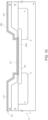
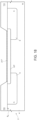
- Figure 1 shows a diode 1, which comprises a semiconductor body 2 formed by silicon, which in turn includes a cathode region 4, which has an N-type doping and is delimited by a front surface S a and by a rear surface S b .
- the cathode region 4 has a peak doping level comprised between 10 13 cm -3 and 10 14 cm -3 .
- the semiconductor body 2 further comprises an anode region 8, which has P-type doping and extends into the cathode region 4, from the front surface S a , so as to form a PN junction with the cathode region 4.
- the anode region 8 has a peak doping level for example comprised between 1*10 14 cm -3 and 1*10 16 cm -3 .
- the anode region 8 may have approximately a circular or polygonal shape.
- the semiconductor body 2 may further comprise a guard ring 9 (optional), which extends into the cathode region 4 from the front surface S a , so as to laterally surround the anode region 8, wherewith it is in direct contact.
- the guard ring 9 has a doping of the P- type, i.e. it has a lower doping level than the doping level of the anode region 8. Furthermore, the guard ring 9 is for preventing the so-called edge breakdown of the anode region 8.
- the semiconductor body 2 may further comprise an enriched anode region 10 (optional), which has a doping of the P+ type (for example, with peak doping level in the order of 1*10 20 cm -3 ) and is for obtaining a different trade-off between switching losses and conduction losses.
- the enriched anode region 10 extends inside an inner portion of the anode region 8, from the front surface S a , without contacting the underlying cathode region 4.
- the enriched anode region 10 may have approximately a circular or polygonal shape.
- the anode region 8 forms a main anode region, in which there may extend the enriched anode region 10.
- the diode 1 further comprises a rear metallization structure 12, which extends underneath the rear surface S b of the cathode region 4.
- the diode 1 further comprises a field oxide region 14, which is formed for example by silicon oxide and extends on the front surface S a , in direct contact with the underlying semiconductor body 2.
- the diode 1 comprises a front dielectric region 16, which extends above the field oxide region 14, wherewith it is in direct contact, and may for example include a dielectric layer stack, which is not shown in detail and may for example include a TEOS oxide layer and an overlying phosphosilicate glass layer.
- the field oxide region 14 and the front dielectric region 16 are traversed by an opening 15, which faces the enriched anode region 10.
- a barrier region 17 extends inside the opening 15, which is formed by cobalt disilicide (CoSi 2 ) and overlies the front surface S a , in direct contact with the underlying enriched anode region 10.
- a peripheral portion of the anode region 8, which is laterally offset with respect to the enriched anode region 10, is overlaid by the field oxide region 14; moreover, without any loss of generality, the portions of the guard ring 9 which are laterally offset with respect to the anode region 8 are overlaid by the field oxide region 14.
- the diode 1 further comprises a front metallization structure 19, which includes at least one metallization region 18, which is formed by aluminum or by a silicon-free aluminum alloy and extends on the front dielectric region 16, as well as inside the opening 15, so as to contact the underlying barrier region 17.
- a front metallization structure 19 which includes at least one metallization region 18, which is formed by aluminum or by a silicon-free aluminum alloy and extends on the front dielectric region 16, as well as inside the opening 15, so as to contact the underlying barrier region 17.
- an inner portion of the metallization region 18 extends inside the opening 15, in direct contact with the enriched anode region 10.
- a peripheral portion of the metallization region 18 extends on a portion of the front dielectric region 16 which laterally delimits the opening 15; this portion of the front dielectric region 16 and an underlying portion of the field oxide region 14 therefore separate the aforementioned peripheral portion of the metallization region 18 from the underlying semiconductor body 2.
- the front metallization structure 19 may comprise further conductive regions; moreover, in a manner known per se, the front metallization structure 19 forms an electrical contact towards the outside world. For instance, a so-called “wire bonding" (not shown) may be formed above the metallization region 18.
- the diode 1 is characterized by high switching speed and a limited increase in the forward voltage and therefore by a good trade-off between switching losses and conduction losses. Furthermore, the Applicant has observed how the use of the barrier region 17 allows to benefit from the advantages conferred by aluminum (in particular, a reduced resistivity and a lower defectiveness with respect to the aluminum-silicon alloy), without the diffusion of aluminum occurring inside the semiconductor body 2.
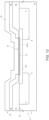
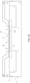
- Figure 2 shows a further embodiment, which is described with reference to the differences with respect to what has been shown in Figure 1 .
- Elements already present in Figure 1 are indicated with the same reference signs, unless otherwise specified.
- the field oxide region (here indicated with 114) is traversed by the opening (here indicated with 115), which faces both the enriched anode region 10 (optional), and therefore the inner portion of the anode region 8, and the peripheral portion of the anode region 8, which, as mentioned, is laterally offset with respect to the enriched anode region 8.
- the barrier region (here indicated with 117) extends into the opening 115, so as to overlie, in direct contact, the enriched anode region 10 and the peripheral portion of the anode region 8.
- the front dielectric region (here indicated with 116) extends, as well as on the field oxide region 114, also on the portion of barrier region 117 that overlies the peripheral portion of the anode region 8, in direct contact. Moreover, the front dielectric region 116 is traversed by a respective opening 125, which is referred to as the top opening 125.
- the top opening 125 faces the portion of barrier region 117 that overlies the enriched anode region 10, and therefore the inner portion of the anode region 8.
- the metallization region (here indicated with 118) extends on the front dielectric region 116 and inside the top opening 125, so as to contact the portion of barrier region 117 that overlies the enriched anode region 10.
- the barrier region 117 forms a shield which extends laterally with respect to the top opening 125, and therefore also with respect to the portion of metallization region 118 that contacts the portion of barrier region 117 that overlies the enriched anode region 10.
- the aforementioned shield is also to prevent the diffusions of aluminum towards the peripheral portion of the anode region 8, and in particular the diffusions that may occur at the bottom corner of the top opening 125, in the direction of the peripheral portion of the anode region 8.
- the embodiment shown in Figure 1 may be manufactured by the process described hereinbelow.
- the cathode region 4 in a manner known per se there are formed the cathode region 4, the guard ring 9 and a first preliminary dielectric region 214, which extends on the front surface S a and includes a thin portion 214', which extends on a portion of cathode region 4 surrounded by the guard ring 9 and on an inner portion of the guard ring 9, and a thick portion 214", which is thicker than the thin portion 214', laterally surrounds the thin portion 214', wherewith it forms a single piece, and overlies an outer portion of the guard ring 9.
- the thin portion 214' has a thickness comprised between 10 and 100nm.
- the thick portion 214" has a thickness at least equal to 100nm.
- the first preliminary dielectric region 214 is intended to form the field oxide region 14.
- the first preliminary dielectric region 214 is formed by thermal oxide.
- the first preliminary dielectric region 214 may be formed by carrying out a first thermal growth, followed by a selective removal of part of the grown thermal oxide, such first thermal growth being then followed by a second thermal growth to form the thin portion 214', where the aforementioned part of grown thermal oxide, as well as the thick portion 214", which comprises thermal oxide grown during the first and the second thermal growths, had previously been selectively removed.
- an ion implantation process of P-type doping species for example, boron
- P-type doping species for example, boron
- these operations lead to the formation of the anode region 8, which extends underneath the thin portion 214' of the first preliminary dielectric region 214, therefore it is laterally offset with respect to the thick portion 214", since the first preliminary dielectric region 214 functions as a mask for the implant.
- the implant may occur, for example, with a dosage comprised between 1e12 cm -2 and 1e13 cm -2 and with energy comprised between 50 and 150 KeV.
- a second preliminary dielectric region 216 is formed, intended to form the front dielectric region 16.
- a plasma or acid etch is performed, by using a respective mask (not shown), so as to selectively remove a part of the thin portion 214' of the first preliminary dielectric region 214 and an overlying portion of the second preliminary dielectric region 216, so as to form the opening 15.
- the remaining portions of the first and the second preliminary dielectric regions 214, 216 form the field oxide region 14 and the front dielectric region 16, respectively.
- a further ion implantation process of P-type doping species is carried out, followed by a respective thermal activation process; the field oxide region 14 and the front dielectric region 16 function as a corresponding mask, in such a way that these operations lead to the formation of the enriched anode region 10.
- the implant may occur, for example, with a dosage comprised between 1e13 cm -2 and 1e16 cm -2 and with energy comprised between 10 and 100 KeV.
- a cobalt sputtering process is performed, in order to form a first metal layer 217, which extends on the front dielectric region 16 and inside the opening 15, in direct contact with the enriched anode region 10.
- the portion of the first metal layer 217 placed in contact with the semiconductor material is indicated with 217', while the portion of the first metal layer 217 spaced apart from the semiconductor material, since it is arranged on the front dielectric region 16, is indicated with 217".
- a second metal layer 230 is formed on the first metal layer 217, for example by sputtering.
- the second metal layer 230 is formed for example by titanium nitride (TiN) and performs a protective function towards the underlying first metal layer 217. In any case, the formation of the second metal layer 230 is optional.
- a so-called rapid thermal process is performed, at a temperature comprised, for example, between 400 and 500°C and with a duration, for example, comprised between 20 and 60 seconds.
- RTP rapid thermal process
- an etch is performed (for example of the wet type, although it may also be of the dry type), in order to remove the second metal layer 230 and the cobalt that has not transformed into cobalt silicide, that is the portion 217" of the first metal layer 217.
- a further rapid thermal process is performed, at a temperature comprised for example between 700 and 950°C and with a duration, for example, comprised between 30 and 120 seconds, so as to transform the cobalt silicide which forms the portion 217' of the first metal layer 217 into cobalt disilicide.
- a temperature comprised for example between 700 and 950°C and with a duration, for example, comprised between 30 and 120 seconds.
- cobalt disilicide has a lower resistivity than cobalt silicide.
- the metallization region 18 is formed, for example by sputtering.
- the manufacturing process may proceed in a manner known per se and therefore not shown, for example with the formation of the rear metallization structure 12.
- an etch is performed (for example of the wet type, although it may also be of the dry type) in order to selectively remove the thin portion 214' of the first preliminary dielectric region 214, so as to expose the anode region 8.
- the opening 115 is formed; moreover, the etch does not involve the thick portion 214" of the first preliminary dielectric region 214, which forms the field oxide region 114.
- a cobalt sputtering process is performed, in order to form the first metal layer 217, which extends on the field oxide region 114 and inside the opening 115, in direct contact with the anode region 8.
- the portion of the first metal layer 217 placed in contact with the semiconductor material is again indicated with 217', while the portion of the first metal layer 217 spaced apart from the semiconductor material, since it is arranged on the field oxide region 114, is indicated with 217".
- the aforementioned second metal layer 230 whose presence is in any case optional, as previously explained, is formed on the first metal layer 217 by sputtering.
- a rapid thermal process is performed, at a temperature comprised, for example, between 400 and 500°C and with a duration, for example, comprised between 20 and 60 seconds.
- a temperature comprised, for example, between 400 and 500°C and with a duration, for example, comprised between 20 and 60 seconds.
- This causes a silicidation of the cobalt placed in contact with the silicon; in other words, the portion 217' of the first metal layer 217 is transformed into cobalt silicide (CoSi), while the portion 217" of the first metal layer 217 remains of cobalt.
- CoSi cobalt silicide
- an etch is performed (for example of the wet type, although it may also be of the dry type), in order to remove the second metal layer 230 and the cobalt that has not transformed into cobalt silicide, that is the portion 217" of the first metal layer 217.
- a further rapid thermal process is performed, at a temperature comprised for example between 700 and 950°C and with a duration, for example, comprised between 30 and 120 seconds, so as to transform the cobalt silicide which forms the portion 217' of the first metal layer 217 into cobalt disilicide.
- a further rapid thermal process is performed, at a temperature comprised for example between 700 and 950°C and with a duration, for example, comprised between 30 and 120 seconds, so as to transform the cobalt silicide which forms the portion 217' of the first metal layer 217 into cobalt disilicide.
- a further rapid thermal process is performed, at a temperature comprised for example between 700 and 950°C and with a duration, for example, comprised between 30 and 120 seconds, so as to transform the cobalt silicide which forms the portion 217' of the first metal layer 217 into cobalt disilicide.
- the portion 217' of the first metal layer 217 is transformed into the barrier region 117.
- the second preliminary dielectric region 216 is formed on the field oxide region 114 and on the barrier region 117.
- an etch is performed (for example of the wet type, although it may also be of the dry type), by using a respective mask (not shown), so as to selectively remove a portion of the second preliminary dielectric region 216 and form the top opening 125.
- the remaining portions of the second preliminary dielectric region 216 form the front dielectric region 16.
- the implant may occur, for example, with a dosage comprised between 1e15 cm -2 and 1e16 cm -2 and with energy comprised between 10 and 100 KeV, while the thermal activation process may occur, for example, at a temperature comprised between 600 and 900°C and with a duration comprised between 30 and 90 minutes.
- the metallization region 118 is formed, for example by sputtering.
- the manufacturing process may proceed in a manner known per se and therefore not described.
- the barrier region and the metallization region form an improved contact structure with respect to the prior art.
- the use of a cobalt disilicide barrier region allows to form a metal-semiconductor junction with ohmic behavior in a diode with an anode region having a low P-type doping level, i.e. in a diode with high switching speed, without using platinum silicide or silicon-enriched aluminum.
- the diode exhibits a reduced forward voltage with respect to what may be obtained in case of a platinum silicide barrier region; moreover, the Applicant has observed how the diode has a temperature coefficient with a modulus that is reduced with respect to what occurs in case of a platinum silicide barrier region, as well as positive in a range of current values comprised between 120A and 200A.
- the guard ring and/or the enriched anode region may be absent, as previously explained.
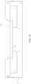
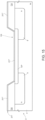
- the enriched anode region 10 is absent, in the embodiment of the type shown in Figure 1 there occurs that the barrier region 17 contacts the inner portion of the anode region 8, as shown in Figure 24 ; furthermore, in the embodiment of the type shown in Figure 2 there occurs that the barrier region 117 contacts either the peripheral portion and the inner portion of the anode region 8, as shown in Figure 25 .
- the ionic implantation process shown in Figure 7 and Figure 22 is thus not carried out.
- composition of the front dielectric region may be different from what has been described.
- the formation of the second metal layer 230 may be absent, as previously mentioned.
- cobalt disilicide may be obtained from cobalt by performing a single rapid thermal process, i.e. without providing for an initial transformation into cobalt silicide, however performing a double rapid thermal process allows to avoid the formation of defectiveness at the edges of the barrier regions.
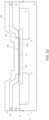
- the semiconductor body 2 may have a structure different from what has been described, as shown as an example in Figure 26 , which, purely by way of example, refers to the embodiment shown in Figure 1 ; however, the same considerations apply also with reference to the other embodiments.
- the semiconductor body 2 comprises a field stop region 104, of the N type, and an enriched cathode region 106, of the N+ type.
- the field stop region 104 extends under the cathode region 4, in direct contact, and has a peak doping level as an example in the order of 10 16 cm -3 ;
- the enriched cathode region 106 extends under the field stop region 104, in direct contact, and has a peak doping level as an example comprised between 1*10 19 cm -3 and 1*10 20 cm -3 .
- the bottom metallization structure 12 extends under the enriched cathode region 106, in direct contact.
Landscapes
- Electrodes Of Semiconductors (AREA)
- Light Receiving Elements (AREA)
Abstract
Description
- The present invention relates to a diode with a contact structure including an improved barrier region and to the related manufacturing process.
- As is known, in the field of semiconductor device manufacturing, the coupling between a semiconductor device and the outside world is made possible by contact structures that include metal regions (also known as metallizations), which are often formed by aluminum and are arranged in contact with the underlying semiconductor material (in particular, silicon).
- Since aluminum tends to diffuse into silicon (a phenomenon also known as "interdiffusion"), with consequent diffusion in the more surface doped areas and shortening with the deeper doped areas of the silicon, appropriate precautions need to be taken to prevent this from happening.
- For example, it is known to overcome the aforementioned problem by adding a certain amount of silicon (for example, with a concentration typically comprised in the range 0.8-2%) in the aluminum region, to reduce the solubility of aluminum in the underlying semiconductor material; however, the material thus formed is characterized by high resistivity and requires the adoption of a relatively complicated manufacturing flow. For this reason, solutions have been proposed over time that provide for the use of one or more barrier layers formed by metal materials other than aluminum, such as titanium and related alloys, which guarantee the formation of good contacts on the semiconductor material and have a reduced solubility compared to aluminum. The barrier layers are interposed between the semiconductor material and the aluminum region.
- In general, metal-semiconductor junctions based on one or more layers of titanium and/or related alloys prove to be satisfactory for contacting N- or P-type semiconductor regions, provided that the doping is sufficiently high (approximately, higher than 1*1016cm-3); conversely, the junction exhibits a non-ohmic, i.e. rectifying, behavior.
- The aforementioned rectifying behavior is particularly evident in case of so-called low efficiency injection anode diode, which are characterized by the presence of an anode region with P-type doping and low doping level (for example, with peak comprised between 1*1014 cm-3 and 1*1016cm-3). In particular, the anode region has a reduced doping to increase the switching speed of the diode, although this involves an increase in the voltage drop in conduction, i.e. an increase in the so-called forward voltage, with the same current flowing through the diode.
- A partial solution to the aforementioned problem of rectifying contacts in case of P-type semiconductive regions with low doping level is to adopt a barrier layer formed by platinum silicide, so as to benefit from the fact that platinum silicide has a lower Schottky barrier potential height than silicon with P-type doping. Unfortunately, however, platinum silicide has a negative forward voltage drop temperature coefficient at high current levels; this causes, in high power applications with multiple diodes connected in parallel, an irreversible imbalance effect, wherein the diode having the lowest voltage drop at the ends thereof draws a large part of the load current, up to reaching the thermal leakage condition and the consequent destruction of the electronic component. Furthermore, this imbalance effect becomes even more critical as the junction temperature increases, since the average lifetime of the minority carriers induced by platinum has a positive temperature coefficient which contributes to further lower the voltage drop of diodes in conduction.
-
US 2017/0186847 A1 discloses a diode according to the preamble of claim 1. The paper " Impact of Elevated Source Drain Architecture on ESD Protection Devices for a 90nm CMOS Technology Node", of Thijs S. et al., ELECTRICAL OVERSTRESS/ELECTROSTATIC DISCHARGE SIMPOSIUM, 2003, EOS/ESD '03, IEEE, Piscataway, NY, USA, 21 September 2003, pp.1-8, discloses a diode with a metallization of copper arranged on a barrier region. - The aim of the present invention is therefore to provide a diode that at least partially overcomes the drawbacks of the prior art.
- According to the present invention, a diode and a manufacturing process are provided as defined in the appended claims.
- For a better understanding of the present invention, preferred embodiments thereof are now described, purely by way of non-limiting example and with reference to the attached drawings, wherein:
-
Figures 1 ,2 ,24 ,25 and26 schematically show cross-sections (not to scale) of embodiments of the present diode; -
Figures 3-13 schematically show cross-sections of the diode shown inFigure 1 , during successive steps of a manufacturing process; and -
Figures 14-23 schematically shown cross-sections of the diode shown inFigure 2 , during successive steps of a manufacturing process. -
Figure 1 shows a diode 1, which comprises asemiconductor body 2 formed by silicon, which in turn includes acathode region 4, which has an N-type doping and is delimited by a front surface Sa and by a rear surface Sb. As an example, thecathode region 4 has a peak doping level comprised between 1013cm-3 and 1014cm-3. - The
semiconductor body 2 further comprises ananode region 8, which has P-type doping and extends into thecathode region 4, from the front surface Sa, so as to form a PN junction with thecathode region 4. Theanode region 8 has a peak doping level for example comprised between 1*1014 cm-3 and 1*1016 cm-3. Although not shown, in top view theanode region 8 may have approximately a circular or polygonal shape. - The
semiconductor body 2 may further comprise a guard ring 9 (optional), which extends into thecathode region 4 from the front surface Sa, so as to laterally surround theanode region 8, wherewith it is in direct contact. Theguard ring 9 has a doping of the P- type, i.e. it has a lower doping level than the doping level of theanode region 8. Furthermore, theguard ring 9 is for preventing the so-called edge breakdown of theanode region 8. - The
semiconductor body 2 may further comprise an enriched anode region 10 (optional), which has a doping of the P+ type (for example, with peak doping level in the order of 1*1020 cm-3) and is for obtaining a different trade-off between switching losses and conduction losses. The enrichedanode region 10 extends inside an inner portion of theanode region 8, from the front surface Sa, without contacting theunderlying cathode region 4. Although not shown, in top view the enrichedanode region 10 may have approximately a circular or polygonal shape. In practice, theanode region 8 forms a main anode region, in which there may extend the enrichedanode region 10. - In a manner known per se, and therefore not shown in detail, the diode 1 further comprises a
rear metallization structure 12, which extends underneath the rear surface Sb of thecathode region 4. - The diode 1 further comprises a
field oxide region 14, which is formed for example by silicon oxide and extends on the front surface Sa, in direct contact with theunderlying semiconductor body 2. - Furthermore, the diode 1 comprises a front
dielectric region 16, which extends above thefield oxide region 14, wherewith it is in direct contact, and may for example include a dielectric layer stack, which is not shown in detail and may for example include a TEOS oxide layer and an overlying phosphosilicate glass layer. - The
field oxide region 14 and the frontdielectric region 16 are traversed by an opening 15, which faces the enrichedanode region 10. Abarrier region 17 extends inside theopening 15, which is formed by cobalt disilicide (CoSi2) and overlies the front surface Sa, in direct contact with the underlying enrichedanode region 10. A peripheral portion of theanode region 8, which is laterally offset with respect to the enrichedanode region 10, is overlaid by thefield oxide region 14; moreover, without any loss of generality, the portions of theguard ring 9 which are laterally offset with respect to theanode region 8 are overlaid by thefield oxide region 14. - The diode 1 further comprises a
front metallization structure 19, which includes at least onemetallization region 18, which is formed by aluminum or by a silicon-free aluminum alloy and extends on the frontdielectric region 16, as well as inside the opening 15, so as to contact theunderlying barrier region 17. - In greater detail, an inner portion of the
metallization region 18 extends inside the opening 15, in direct contact with the enrichedanode region 10. A peripheral portion of themetallization region 18 extends on a portion of the frontdielectric region 16 which laterally delimits theopening 15; this portion of the frontdielectric region 16 and an underlying portion of thefield oxide region 14 therefore separate the aforementioned peripheral portion of themetallization region 18 from theunderlying semiconductor body 2. - Although not shown, the
front metallization structure 19 may comprise further conductive regions; moreover, in a manner known per se, thefront metallization structure 19 forms an electrical contact towards the outside world. For instance, a so-called "wire bonding" (not shown) may be formed above themetallization region 18. - In practice, owing to the reduced doping of the
anode region 8, the diode 1 is characterized by high switching speed and a limited increase in the forward voltage and therefore by a good trade-off between switching losses and conduction losses. Furthermore, the Applicant has observed how the use of thebarrier region 17 allows to benefit from the advantages conferred by aluminum (in particular, a reduced resistivity and a lower defectiveness with respect to the aluminum-silicon alloy), without the diffusion of aluminum occurring inside thesemiconductor body 2. -
Figure 2 shows a further embodiment, which is described with reference to the differences with respect to what has been shown inFigure 1 . Elements already present inFigure 1 are indicated with the same reference signs, unless otherwise specified. - In detail, the field oxide region (here indicated with 114) is traversed by the opening (here indicated with 115), which faces both the enriched anode region 10 (optional), and therefore the inner portion of the
anode region 8, and the peripheral portion of theanode region 8, which, as mentioned, is laterally offset with respect to the enrichedanode region 8. - The barrier region (here indicated with 117) extends into the opening 115, so as to overlie, in direct contact, the enriched
anode region 10 and the peripheral portion of theanode region 8. - The front dielectric region (here indicated with 116) extends, as well as on the
field oxide region 114, also on the portion ofbarrier region 117 that overlies the peripheral portion of theanode region 8, in direct contact. Moreover, the frontdielectric region 116 is traversed by arespective opening 125, which is referred to as the top opening 125. - In detail, the
top opening 125 faces the portion ofbarrier region 117 that overlies the enrichedanode region 10, and therefore the inner portion of theanode region 8. - The metallization region (here indicated with 118) extends on the front
dielectric region 116 and inside the top opening 125, so as to contact the portion ofbarrier region 117 that overlies the enrichedanode region 10. - In practice, in the embodiment shown in
Figure 2 , thebarrier region 117 forms a shield which extends laterally with respect to thetop opening 125, and therefore also with respect to the portion ofmetallization region 118 that contacts the portion ofbarrier region 117 that overlies the enrichedanode region 10. The aforementioned shield is also to prevent the diffusions of aluminum towards the peripheral portion of theanode region 8, and in particular the diffusions that may occur at the bottom corner of the top opening 125, in the direction of the peripheral portion of theanode region 8. - That said, the embodiment shown in
Figure 1 may be manufactured by the process described hereinbelow. - Initially, as shown in
Figure 3 , in a manner known per se there are formed thecathode region 4, theguard ring 9 and a first preliminarydielectric region 214, which extends on the front surface Sa and includes a thin portion 214', which extends on a portion ofcathode region 4 surrounded by theguard ring 9 and on an inner portion of theguard ring 9, and athick portion 214", which is thicker than the thin portion 214', laterally surrounds the thin portion 214', wherewith it forms a single piece, and overlies an outer portion of theguard ring 9. For instance, the thin portion 214' has a thickness comprised between 10 and 100nm. Thethick portion 214" has a thickness at least equal to 100nm. The first preliminarydielectric region 214 is intended to form thefield oxide region 14. - In greater detail, the first preliminary
dielectric region 214 is formed by thermal oxide. For instance, although not shown in detail, the first preliminarydielectric region 214 may be formed by carrying out a first thermal growth, followed by a selective removal of part of the grown thermal oxide, such first thermal growth being then followed by a second thermal growth to form the thin portion 214', where the aforementioned part of grown thermal oxide, as well as thethick portion 214", which comprises thermal oxide grown during the first and the second thermal growths, had previously been selectively removed. - Then, as shown in
Figure 4 , an ion implantation process of P-type doping species (for example, boron), indicated byarrows 208, is carried out, followed by a thermal activation process; these operations lead to the formation of theanode region 8, which extends underneath the thin portion 214' of the first preliminarydielectric region 214, therefore it is laterally offset with respect to thethick portion 214", since the first preliminarydielectric region 214 functions as a mask for the implant. Moreover, the implant may occur, for example, with a dosage comprised between 1e12 cm-2 and 1e13 cm-2 and with energy comprised between 50 and 150 KeV. - Subsequently, as shown in
Figure 5 , above the first preliminary dielectric region 214 a second preliminarydielectric region 216 is formed, intended to form the frontdielectric region 16. - Then, as shown in
Figure 6 , a plasma or acid etch is performed, by using a respective mask (not shown), so as to selectively remove a part of the thin portion 214' of the first preliminarydielectric region 214 and an overlying portion of the second preliminarydielectric region 216, so as to form theopening 15. The remaining portions of the first and the second preliminarydielectric regions field oxide region 14 and the frontdielectric region 16, respectively. - Then, as shown in
Figure 7 , a further ion implantation process of P-type doping species, indicated byarrows 210, is carried out, followed by a respective thermal activation process; thefield oxide region 14 and the frontdielectric region 16 function as a corresponding mask, in such a way that these operations lead to the formation of the enrichedanode region 10. Moreover, the implant may occur, for example, with a dosage comprised between 1e13 cm-2 and 1e16 cm-2 and with energy comprised between 10 and 100 KeV. - Subsequently, as shown in
Figure 8 , a cobalt sputtering process is performed, in order to form afirst metal layer 217, which extends on the frontdielectric region 16 and inside theopening 15, in direct contact with the enrichedanode region 10. - In greater detail, the portion of the
first metal layer 217 placed in contact with the semiconductor material (in particular, with the enriched anode region 10) is indicated with 217', while the portion of thefirst metal layer 217 spaced apart from the semiconductor material, since it is arranged on the frontdielectric region 16, is indicated with 217". - Then, as shown in
Figure 9 , asecond metal layer 230 is formed on thefirst metal layer 217, for example by sputtering. Thesecond metal layer 230 is formed for example by titanium nitride (TiN) and performs a protective function towards the underlyingfirst metal layer 217. In any case, the formation of thesecond metal layer 230 is optional. - Then, as shown in
Figure 10 , a so-called rapid thermal process (RTP) is performed, at a temperature comprised, for example, between 400 and 500°C and with a duration, for example, comprised between 20 and 60 seconds. This causes a silicidation of the cobalt placed in contact with the silicon; in other words, the portion 217' of thefirst metal layer 217 is transformed into cobalt silicide (CoSi), while theportion 217" of thefirst metal layer 217 remains of cobalt. - Subsequently, as shown in
Figure 11 , an etch is performed (for example of the wet type, although it may also be of the dry type), in order to remove thesecond metal layer 230 and the cobalt that has not transformed into cobalt silicide, that is theportion 217" of thefirst metal layer 217. - Then, as shown in
Figure 12 , a further rapid thermal process is performed, at a temperature comprised for example between 700 and 950°C and with a duration, for example, comprised between 30 and 120 seconds, so as to transform the cobalt silicide which forms the portion 217' of thefirst metal layer 217 into cobalt disilicide. In this manner, the portion 217' of thefirst metal layer 217 is transformed into thebarrier region 17. In this regard, cobalt disilicide has a lower resistivity than cobalt silicide. - Subsequently, as shown in
Figure 13 , themetallization region 18 is formed, for example by sputtering. - Then, the manufacturing process may proceed in a manner known per se and therefore not shown, for example with the formation of the
rear metallization structure 12. - Instead, as regards the embodiment shown in
Figure 2 , it may be manufactured by following the process described hereinbelow. - Initially, the same operations described with reference to
Figures 3 and4 are performed. - Subsequently, an etch is performed (for example of the wet type, although it may also be of the dry type) in order to selectively remove the thin portion 214' of the first preliminary
dielectric region 214, so as to expose theanode region 8. In this manner, as shown inFigure 14 , theopening 115 is formed; moreover, the etch does not involve thethick portion 214" of the first preliminarydielectric region 214, which forms thefield oxide region 114. - Then, as shown in
Figure 15 , a cobalt sputtering process is performed, in order to form thefirst metal layer 217, which extends on thefield oxide region 114 and inside theopening 115, in direct contact with theanode region 8. - In greater detail, the portion of the
first metal layer 217 placed in contact with the semiconductor material (in particular, with the anode region 8) is again indicated with 217', while the portion of thefirst metal layer 217 spaced apart from the semiconductor material, since it is arranged on thefield oxide region 114, is indicated with 217". - Subsequently, as shown in
Figure 16 , the aforementionedsecond metal layer 230, whose presence is in any case optional, as previously explained, is formed on thefirst metal layer 217 by sputtering. - Then, as shown in
Figure 17 , a rapid thermal process is performed, at a temperature comprised, for example, between 400 and 500°C and with a duration, for example, comprised between 20 and 60 seconds. This causes a silicidation of the cobalt placed in contact with the silicon; in other words, the portion 217' of thefirst metal layer 217 is transformed into cobalt silicide (CoSi), while theportion 217" of thefirst metal layer 217 remains of cobalt. - Subsequently, as shown in
Figure 18 , an etch is performed (for example of the wet type, although it may also be of the dry type), in order to remove thesecond metal layer 230 and the cobalt that has not transformed into cobalt silicide, that is theportion 217" of thefirst metal layer 217. - Then, as shown in
Figure 19 , a further rapid thermal process is performed, at a temperature comprised for example between 700 and 950°C and with a duration, for example, comprised between 30 and 120 seconds, so as to transform the cobalt silicide which forms the portion 217' of thefirst metal layer 217 into cobalt disilicide. In this manner, the portion 217' of thefirst metal layer 217 is transformed into thebarrier region 117. - Subsequently, as shown in
Figure 20 , the second preliminarydielectric region 216 is formed on thefield oxide region 114 and on thebarrier region 117. - Then, as shown in
Figure 21 , an etch is performed (for example of the wet type, although it may also be of the dry type), by using a respective mask (not shown), so as to selectively remove a portion of the second preliminarydielectric region 216 and form thetop opening 125. The remaining portions of the second preliminarydielectric region 216 form the frontdielectric region 16. - Then, as shown in
Figure 22 , a further ion implantation process of P-type doping species, indicated byarrows 250, is carried out followed by a respective thermal activation process; the frontdielectric region 116 functions as a corresponding mask, in such a way that these operations lead to the formation of the enrichedanode region 10. Moreover, the implant may occur, for example, with a dosage comprised between 1e15 cm-2 and 1e16 cm-2 and with energy comprised between 10 and 100 KeV, while the thermal activation process may occur, for example, at a temperature comprised between 600 and 900°C and with a duration comprised between 30 and 90 minutes. - Then, as shown in
Figure 23 , themetallization region 118 is formed, for example by sputtering. - Subsequently, the manufacturing process may proceed in a manner known per se and therefore not described.
- The advantages that the present solution affords are clear from what has been previously described and illustrated. In practice, the barrier region and the metallization region form an improved contact structure with respect to the prior art.
- In particular, the use of a cobalt disilicide barrier region allows to form a metal-semiconductor junction with ohmic behavior in a diode with an anode region having a low P-type doping level, i.e. in a diode with high switching speed, without using platinum silicide or silicon-enriched aluminum. In this manner, the diode exhibits a reduced forward voltage with respect to what may be obtained in case of a platinum silicide barrier region; moreover, the Applicant has observed how the diode has a temperature coefficient with a modulus that is reduced with respect to what occurs in case of a platinum silicide barrier region, as well as positive in a range of current values comprised between 120A and 200A.
- Finally, it is clear that modifications and variations may be made to what has been described and illustrated so far, without however departing from the scope of the present invention, as defined in the attached claims.
- For example, the guard ring and/or the enriched anode region may be absent, as previously explained. In case the enriched
anode region 10 is absent, in the embodiment of the type shown inFigure 1 there occurs that thebarrier region 17 contacts the inner portion of theanode region 8, as shown inFigure 24 ; furthermore, in the embodiment of the type shown inFigure 2 there occurs that thebarrier region 117 contacts either the peripheral portion and the inner portion of theanode region 8, as shown inFigure 25 . In the manufacturing process, the ionic implantation process shown inFigure 7 andFigure 22 is thus not carried out. - The composition of the front dielectric region may be different from what has been described.
- Regarding the manufacturing process, the formation of the
second metal layer 230 may be absent, as previously mentioned. Moreover, cobalt disilicide may be obtained from cobalt by performing a single rapid thermal process, i.e. without providing for an initial transformation into cobalt silicide, however performing a double rapid thermal process allows to avoid the formation of defectiveness at the edges of the barrier regions. - In addition, all the ion implantation operations described may provide for the use of respective additional masks.
- Finally, the
semiconductor body 2 may have a structure different from what has been described, as shown as an example inFigure 26 , which, purely by way of example, refers to the embodiment shown inFigure 1 ; however, the same considerations apply also with reference to the other embodiments. - In detail, the
semiconductor body 2 comprises a field stop region 104, of the N type, and an enrichedcathode region 106, of the N+ type. In particular, the field stop region 104 extends under thecathode region 4, in direct contact, and has a peak doping level as an example in the order of 1016cm-3; the enrichedcathode region 106 extends under the field stop region 104, in direct contact, and has a peak doping level as an example comprised between 1*1019cm-3 and 1*1020cm-3. Thebottom metallization structure 12 extends under the enrichedcathode region 106, in direct contact.
Claims (15)
- A diode comprising a semiconductor body (2) of silicon including:- a cathode region (4), which has a first conductivity type and is delimited by a front surface (Sa); and- an anode region (8,10), which has a second conductivity type and extends into the cathode region (4) from the front surface (Sa);
said diode (1) further comprising:- a barrier region (17;117) of cobalt disilicide, arranged on the anode region (8,10); and- a metallization region (18; 118) of aluminum or of an aluminum alloy, arranged on the barrier region (17;117);
characterized in that the barrier region (17;117) contacts the anode region (8,10). - The diode according to claim 1, wherein the anode region (8,10) has a P-type conductivity and comprises a main anode region (8), which extends in the cathode region (4) starting from the front surface (Sa) and has a peak doping level comprised between 1*1014 cm-3 and 1*1016 cm-3.
- The diode according to claim 2, wherein the main anode region (8) comprises an inner portion and a peripheral portion, said diode (1) further comprising:- a field oxide region (14), which extends on the semiconductor body (2); and- a front dielectric region (16), arranged on the field oxide region (14);
and wherein the field oxide region (14) and the front dielectric region (16) are traversed by a first opening (15) which faces the inner portion of the main anode region (8), the field oxide region (14) extending on the peripheral portion of the main anode region (8) ; and wherein the barrier region (17) extends inside the first opening (15), in direct contact with the inner portion of the main anode region (8). - The diode according to claim 3, wherein the metallization region (18) extends on the front dielectric region (16) and inside the first opening (15).
- The diode according to claim 2, wherein the main anode region (8) comprises an inner portion and a peripheral portion, said diode (1) further comprising:- a field oxide region (114), which extends on the semiconductor body (2) and is traversed by a first opening (115), which faces the inner portion and the peripheral portion of the main anode region (8), the barrier region (117) extending inside the first opening (115), on the inner portion and on the peripheral portion of the main anode region (8); and- a front dielectric region (116), which extends on the field oxide region (114) and on a portion of the barrier region (117) arranged on the peripheral portion of the main anode region (8), said front dielectric region (116) being traversed by a second opening (125) which faces a portion of the barrier region (117) arranged on the inner portion of the main anode region (8);
and wherein the metallization region (118) extends on the front dielectric region (116) and on said portion of the barrier region (117) arranged on the inner portion of the main anode region (8). - The diode according to claim 2, wherein the main anode region (8) comprises an inner portion and a peripheral portion; and wherein the anode region (8,10) further comprises an enriched anode region (10), which extends into the inner portion of the main anode region (8) and has a higher doping level than the doping level of the main anode region (8), said diode (1) further comprising:- a field oxide region (14), which extends on the semiconductor body (2); and- a front dielectric region (16), arranged on the field oxide region (14);
and wherein the field oxide region (14) and the front dielectric region (16) are traversed by a first opening (15) that faces the enriched anode region (10), the field oxide region (14) extending on the peripheral portion of the main anode region (8); and wherein the barrier region (17) extends inside the first opening (15), on the enriched anode region (10) . - The diode according to claim 2, wherein the main anode region (8) comprises an inner portion and a peripheral portion; and wherein the anode region (8,10) further comprises an enriched anode region (10), which extends into the inner portion of the main anode region (8) and has a higher doping level than the doping level of the main anode region (8), said diode (1) further comprising:- a field oxide region (114), which extends on the semiconductor body (2) and is traversed by a first opening (115), which faces the enriched anode region (10) and the peripheral portion of the main anode region (8), the barrier region (117) extending inside the first opening (115), on the enriched anode region (10) and the peripheral portion of the main anode region (8); and- a front dielectric region (116), which extends on the field oxide region (114) and on a portion of the barrier region (117) arranged on the peripheral portion of the main anode region (8), said front dielectric region (116) being traversed by a second opening (125) which faces a portion of the barrier region (117) arranged on the enriched anode region (10);
and wherein the metallization region (118) extends on the front dielectric region (116) and on said portion of the barrier region (117) arranged on the enriched anode region (10) . - A process for manufacturing a diode (1), comprising:- forming a semiconductor body (2) of silicon including a cathode region (4), which has a first conductivity type and is delimited by a front surface (Sa), and an anode region (8,10), which has a second conductivity type and extends into the cathode region (4) from the front surface (Sa);- on the anode region (8,10), forming a barrier region (17;117) of cobalt disilicide; and- on the barrier region (17;117), forming a metallization region (18;118) of aluminum or of an aluminum alloy;
characterized in that the barrier region (17;117) contacts the anode region (8,10). - The manufacturing process according to claim 8, wherein the anode region (8,10) has a P-type conductivity and comprises a main anode region (8), which extends in the cathode region (4) starting from the front surface (Sa) and has a peak doping level comprised between 1*1014 cm-3 and 1*1016 cm-3.
- The manufacturing process according to claim 9, further comprising:- on the semiconductor body (2), forming a first preliminary dielectric region (214) including a respective thin portion (214') and a respective thick portion (214"), which surrounds the thin portion (214');- forming the main anode region (8) underneath the thin portion (214') of the first preliminary dielectric region (214), the main anode region (8) comprising a respective inner portion and a respective peripheral portion; and subsequently- on the first preliminary dielectric region (214), forming a second preliminary dielectric region (216);- selectively removing a portion of the second preliminary dielectric region (216) and an underlying part of the thin portion (214') of the first preliminary dielectric region (214), so as to form a first opening (15) which faces the inner portion of the main anode region (8), the residual portions of the first and the second preliminary dielectric regions (214,216) respectively forming a field oxide region (14), which extends on the peripheral portion of the main anode region (8), and a front dielectric region (16) ;
and wherein forming the barrier region (17) comprises forming the barrier region (17) inside the first opening (15), in direct contact with the inner portion of the main anode region (8); and wherein forming the metallization region (118) comprises forming the metallization region (118) on the front dielectric region (16) and inside the first opening (15). - The manufacturing process according to claim 9, further comprising:- on the semiconductor body (2), forming a first preliminary dielectric region (214) including a respective thin portion (214') and a respective thick portion (214"), which surrounds the thin portion (214');- forming the main anode region (8) underneath the thin portion (214') of the first preliminary dielectric region (214), the main anode region (8) comprising a respective inner portion and a respective peripheral portion; and subsequently- on the first preliminary dielectric region (214), forming a second preliminary dielectric region (216);- selectively removing a portion of the second preliminary dielectric region (216) and an underlying part of the thin portion (214') of the first preliminary dielectric region (214), so as to form a first opening (15) which faces the inner portion of the main anode region (8), the residual portions of the first and the second preliminary dielectric regions (214,216) respectively forming a field oxide region (14), which extends on the peripheral portion of the main anode region (8), and a front dielectric region (16) ;- through the first opening (15), forming an enriched anode region (10), which extends in the inner portion of the main anode region (8) and has a higher doping level than the doping level of the main anode region (8);
and wherein forming the barrier region (17) comprises forming the barrier region (17) inside the first opening (15), in direct contact with the enriched anode region (10); and wherein forming the metallization region (118) comprises forming the metallization region (118) on the front dielectric region (16) and inside the first opening (15). - The manufacturing process according to claim 10 or 11, wherein forming the barrier region (17) comprises:- forming a conductive layer (217) of cobalt including a first portion (217'), arranged inside the first opening (15), and a second portion (217"), arranged on the front dielectric region (16);- performing a first thermal process to transform the cobalt of the first portion (217') of the conductive layer (217) into cobalt silicide; and subsequently- selectively removing the second portion (217") of the conductive layer (217); and subsequently- performing a second thermal process to transform the cobalt silicide of the first portion (217') of the conductive layer (217) into cobalt disilicide.
- The manufacturing process according to claim 9, further comprising:- on the semiconductor body (2), forming a first preliminary dielectric region (214) including a respective thin portion (214') and a respective thick portion (214"), which surrounds the thin portion (214');- forming the main anode region (8) underneath the thin portion (214') of the first preliminary dielectric region (214), said main anode region (8) comprising a respective inner portion and a peripheral portion;- selectively removing the thin portion (214') of the first preliminary dielectric region (214), so as to form a first opening (115) which faces the inner portion and the peripheral portion of the main anode region (8), the remaining portion of the first preliminary dielectric region (214) forming a field oxide region (114);
and wherein forming the barrier region (117) comprises forming the barrier region (117) inside the first opening (115), in direct contact with the inner portion and the peripheral portion of the main anode region (8); said manufacturing process further comprising:- forming a second preliminary dielectric region (216) on the barrier region (117) and on the field oxide region (114); and subsequently- selectively removing a portion of the second preliminary dielectric region (216), so as to form a second opening (125) which faces a portion of the barrier region (117) that overlies the inner portion of the main anode region (8), the remaining portion of the second preliminary dielectric region (216) forming a front dielectric region (116); and subsequently- forming the metallization region (118) on the front dielectric region (116) and on said portion of the barrier region (117) that overlies the inner portion of the main anode region (8). - The manufacturing process according to claim 9, further comprising:- on the semiconductor body (2), forming a first preliminary dielectric region (214) including a respective thin portion (214') and a respective thick portion (214"), which surrounds the thin portion (214');- forming the main anode region (8) underneath the thin portion (214') of the first preliminary dielectric region (214), said main anode region (8) comprising a respective inner portion and a peripheral portion;- selectively removing the thin portion (214') of the first preliminary dielectric region (214), so as to form a first opening (115) which faces the inner portion and the peripheral portion of the main anode region (8), the remaining portion of the first preliminary dielectric region (214) forming a field oxide region (114);
and wherein forming the barrier region (117) comprises forming the barrier region (117) inside the first opening (115), in direct contact with the inner portion and the peripheral portion of the main anode region (8); said manufacturing process further comprising:- forming a second preliminary dielectric region (216) on the barrier region (117) and on the field oxide region (114); and subsequently- selectively removing a portion of the second preliminary dielectric region (216), so as to form a second opening (125) which faces a portion of the barrier region (117) that overlies the inner portion of the main anode region (8), the remaining portion of the second preliminary dielectric region (216) forming a front dielectric region (116); and subsequently- through the second opening (125), forming an enriched anode region (10), which extends in the inner portion of the main anode region (8) and has a higher doping level than the doping level of the main anode region (8); and subsequently- forming the metallization region (118) on the front dielectric region (116) and on said portion of the barrier region (117) that overlies the inner portion of the main anode region (8). - The manufacturing process according to claim 13 or 14, wherein forming the barrier region (17) comprises:- forming a conductive layer (217) of cobalt including a first portion (217'), arranged inside the first opening (115), and a second portion (217"), arranged on the field oxide region (114);- performing a first thermal process to transform the cobalt of the first portion (217') of the conductive layer (217) into cobalt silicide; and subsequently- selectively removing the second portion (217") of the conductive layer (217); and subsequently- performing a second thermal process to transform the cobalt silicide of the first portion (217') of the conductive layer (217) into cobalt disilicide.
Applications Claiming Priority (1)
| Application Number | Priority Date | Filing Date | Title |
|---|---|---|---|
| IT102022000000203A IT202200000203A1 (en) | 2022-01-10 | 2022-01-10 | DIODE WITH CONTACT STRUCTURE INCLUDING AN IMPROVED BARRIER REGION AND RELEVANT MANUFACTURING PROCESS |
Publications (1)
| Publication Number | Publication Date |
|---|---|
| EP4210115A1 true EP4210115A1 (en) | 2023-07-12 |
Family
ID=80685324
Family Applications (1)
| Application Number | Title | Priority Date | Filing Date |
|---|---|---|---|
| EP22212787.0A Pending EP4210115A1 (en) | 2022-01-10 | 2022-12-12 | Diode with contact structure including an improved barrier region and related manufacturing process |
Country Status (3)
| Country | Link |
|---|---|
| US (1) | US12622040B2 (en) |
| EP (1) | EP4210115A1 (en) |
| IT (1) | IT202200000203A1 (en) |
Citations (7)
| Publication number | Priority date | Publication date | Assignee | Title |
|---|---|---|---|---|
| US20050026379A1 (en) * | 2003-07-31 | 2005-02-03 | Thorsten Kammler | Polysilicon line having a metal silicide region enabling linewidth scaling |
| EP2341528A1 (en) * | 2010-01-05 | 2011-07-06 | ABB Technology AG | Power Semiconductor Device and its manufacturing method |
| WO2014202750A1 (en) * | 2013-06-20 | 2014-12-24 | Abb Technology Ag | Fast recovery diode |
| US20150115449A1 (en) * | 2013-10-31 | 2015-04-30 | Infineon Technologies Ag | Semiconductor Device Having a Corrosion-Resistant Metallization and Method for Manufacturing Thereof |
| US20150303268A1 (en) * | 2013-01-18 | 2015-10-22 | Hitachi Power Semiconductor Device, Ltd. | Diode and power conversion device |
| US20170186847A1 (en) | 2015-12-25 | 2017-06-29 | Rohm Co., Ltd. | Semiconductor device and method for manufacturing semiconductor device |
| EP3196943A1 (en) * | 2016-01-22 | 2017-07-26 | ABB Technology AG | Bipolar diode and method for manufacturing such a diode |
Family Cites Families (7)
| Publication number | Priority date | Publication date | Assignee | Title |
|---|---|---|---|---|
| US7279390B2 (en) | 2005-03-21 | 2007-10-09 | Semiconductor Components Industries, L.L.C. | Schottky diode and method of manufacture |
| JP6995725B2 (en) * | 2018-09-19 | 2022-01-17 | 株式会社東芝 | Semiconductor device |
| US11309438B2 (en) * | 2019-12-10 | 2022-04-19 | Fuji Electric Co., Ltd. | Silicon carbide semiconductor device and method of manufacturing silicon carbide semiconductor device |
| JP7371507B2 (en) * | 2020-01-22 | 2023-10-31 | 富士電機株式会社 | Method for manufacturing silicon carbide semiconductor device |
| JP7305591B2 (en) | 2020-03-24 | 2023-07-10 | 株式会社東芝 | semiconductor equipment |
| JP7505278B2 (en) * | 2020-06-11 | 2024-06-25 | 富士電機株式会社 | Silicon carbide semiconductor device |
| CN220189657U (en) | 2022-01-10 | 2023-12-15 | 意法半导体股份有限公司 | Semiconductor diode and semiconductor device |
-
2022
- 2022-01-10 IT IT102022000000203A patent/IT202200000203A1/en unknown
- 2022-12-12 EP EP22212787.0A patent/EP4210115A1/en active Pending
-
2023
- 2023-01-04 US US18/150,118 patent/US12622040B2/en active Active
Patent Citations (7)
| Publication number | Priority date | Publication date | Assignee | Title |
|---|---|---|---|---|
| US20050026379A1 (en) * | 2003-07-31 | 2005-02-03 | Thorsten Kammler | Polysilicon line having a metal silicide region enabling linewidth scaling |
| EP2341528A1 (en) * | 2010-01-05 | 2011-07-06 | ABB Technology AG | Power Semiconductor Device and its manufacturing method |
| US20150303268A1 (en) * | 2013-01-18 | 2015-10-22 | Hitachi Power Semiconductor Device, Ltd. | Diode and power conversion device |
| WO2014202750A1 (en) * | 2013-06-20 | 2014-12-24 | Abb Technology Ag | Fast recovery diode |
| US20150115449A1 (en) * | 2013-10-31 | 2015-04-30 | Infineon Technologies Ag | Semiconductor Device Having a Corrosion-Resistant Metallization and Method for Manufacturing Thereof |
| US20170186847A1 (en) | 2015-12-25 | 2017-06-29 | Rohm Co., Ltd. | Semiconductor device and method for manufacturing semiconductor device |
| EP3196943A1 (en) * | 2016-01-22 | 2017-07-26 | ABB Technology AG | Bipolar diode and method for manufacturing such a diode |
Non-Patent Citations (4)
| Title |
|---|
| BROADBENT E K ET AL: "SELF-ALIGNED SILICIDED (PTSI AND COSI2) ULTRA-SHALLOW P+/N JUNCTIONS", IEEE ELECTRON DEVICE LETTERS, IEEE, USA, vol. EDL-08, no. 7, 1 July 1987 (1987-07-01), pages 318 - 320, XP000819044, ISSN: 0741-3106 * |
| THIJS S ET AL: "Impact of elevated source drain architecture on ESD protection devices for a 90nm CMOS technology node", ELECTRICAL OVERSTRESS/ELECTROSTATIC DISCHARGE SYMPOSIUM, 2003. EOS/ESD '03, IEEE, PISCATAWAY, NJ, USA, 21 September 2003 (2003-09-21), pages 1 - 8, XP031533898, ISBN: 978-1-58537-057-3 * |
| THIJS S. ET AL.: "ELECTRICAL", 21 September 2003, IEEE, article "Impact of Elevated Source Drain Architecture on ESD Protection Devices for a 90nm CMOS Technology Node", pages: 1 - 8 |
| ZHANG S-L ET AL: "Self-aligned silicides for Ohmic contacts in complementary metal-oxide-semiconductor technology: TiSi2, CoSi2, and NiSi", JOURNAL OF VACUUM SCIENCE, AMERICAN INSTITUTE OF PHYSICS, 2 HUNTINGTON QUADRANGLE, MELVILLE, NY 11747, vol. 22, no. 4, 1 July 2004 (2004-07-01), pages 1361 - 1370, XP012073738, ISSN: 0734-2101, DOI: 10.1116/1.1688364 * |
Also Published As
| Publication number | Publication date |
|---|---|
| US12622040B2 (en) | 2026-05-05 |
| US20230223458A1 (en) | 2023-07-13 |
| IT202200000203A1 (en) | 2023-07-10 |
Similar Documents
| Publication | Publication Date | Title |
|---|---|---|
| US9905666B2 (en) | Trench schottky rectifier device and method for manufacturing the same | |
| CN108039360B (en) | Edge termination structure employing recesses for edge termination elements | |
| US8338906B2 (en) | Schottky device | |
| US6998694B2 (en) | High switching speed two mask Schottky diode with high field breakdown | |
| US9064904B2 (en) | MOS P-N junction Schottky diode device and method for manufacturing the same | |
| US6825073B1 (en) | Schottky diode with high field breakdown and low reverse leakage current | |
| US20100258899A1 (en) | Schottky diode device with an extended guard ring and fabrication method thereof | |
| US7880166B2 (en) | Fast recovery reduced p-n junction rectifier | |
| US8728878B2 (en) | MOS P-N junction diode device and method for manufacturing the same | |
| CN220189657U (en) | Semiconductor diode and semiconductor device | |
| JP2003258271A (en) | Silicon carbide Schottky diode and method of manufacturing the same | |
| US9406788B2 (en) | Structure of a trench MOS rectifier and method of forming the same | |
| US20080258263A1 (en) | High Current Steering ESD Protection Zener Diode And Method | |
| US20170133480A1 (en) | Mos p-n junction diode with enhanced response speed and manufacturing method thereof | |
| US7368371B2 (en) | Silicon carbide Schottky diode and method of making the same | |
| US12622040B2 (en) | Diode with contact structure including an improved barrier region and related manufacturing process | |
| JP6540547B2 (en) | MPS diode | |
| US7906386B2 (en) | Semiconductor device and method of fabricating the same | |
| KR20200027902A (en) | Structure and method for sic based protection device | |
| KR100598348B1 (en) | Schottky Diode Manufacturing Method Using Silicon-based CMOS Process | |
| CN116417521A (en) | Diode with contact structure including improved barrier region and process for manufacturing the same | |
| US20250311399A1 (en) | Reverse-conducting igbt device with low efficiency injection anode and manufacturing process thereof | |
| US20250107117A1 (en) | Schottky diode with low reverse current and high heat dissipation effect | |
| WO2025192748A1 (en) | Semiconductor device | |
| US20070293028A1 (en) | Method of forming low forward voltage Shottky barrier diode with LOCOS structure therein |
Legal Events
| Date | Code | Title | Description |
|---|---|---|---|
| PUAI | Public reference made under article 153(3) epc to a published international application that has entered the european phase |
Free format text: ORIGINAL CODE: 0009012 |
|
| STAA | Information on the status of an ep patent application or granted ep patent |
Free format text: STATUS: THE APPLICATION HAS BEEN PUBLISHED |
|
| AK | Designated contracting states |
Kind code of ref document: A1 Designated state(s): AL AT BE BG CH CY CZ DE DK EE ES FI FR GB GR HR HU IE IS IT LI LT LU LV MC ME MK MT NL NO PL PT RO RS SE SI SK SM TR |
|
| STAA | Information on the status of an ep patent application or granted ep patent |
Free format text: STATUS: REQUEST FOR EXAMINATION WAS MADE |
|
| 17P | Request for examination filed |
Effective date: 20231023 |
|
| RBV | Designated contracting states (corrected) |
Designated state(s): AL AT BE BG CH CY CZ DE DK EE ES FI FR GB GR HR HU IE IS IT LI LT LU LV MC ME MK MT NL NO PL PT RO RS SE SI SK SM TR |
|
| STAA | Information on the status of an ep patent application or granted ep patent |
Free format text: STATUS: EXAMINATION IS IN PROGRESS |
|
| 17Q | First examination report despatched |
Effective date: 20250516 |