EP4207967A2 - Organic light emitting diode and organic light emitting display device including the same - Google Patents
Organic light emitting diode and organic light emitting display device including the same Download PDFInfo
- Publication number
- EP4207967A2 EP4207967A2 EP22203390.4A EP22203390A EP4207967A2 EP 4207967 A2 EP4207967 A2 EP 4207967A2 EP 22203390 A EP22203390 A EP 22203390A EP 4207967 A2 EP4207967 A2 EP 4207967A2
- Authority
- EP
- European Patent Office
- Prior art keywords
- blue
- organic light
- emitting
- light emitting
- compound
- Prior art date
- Legal status (The legal status is an assumption and is not a legal conclusion. Google has not performed a legal analysis and makes no representation as to the accuracy of the status listed.)
- Pending
Links
Images


Classifications
-
- H—ELECTRICITY
- H10—SEMICONDUCTOR DEVICES; ELECTRIC SOLID-STATE DEVICES NOT OTHERWISE PROVIDED FOR
- H10K—ORGANIC ELECTRIC SOLID-STATE DEVICES
- H10K50/00—Organic light-emitting devices
- H10K50/80—Constructional details
- H10K50/805—Electrodes
- H10K50/81—Anodes
- H10K50/818—Reflective anodes, e.g. ITO combined with thick metallic layers
-
- C—CHEMISTRY; METALLURGY
- C09—DYES; PAINTS; POLISHES; NATURAL RESINS; ADHESIVES; COMPOSITIONS NOT OTHERWISE PROVIDED FOR; APPLICATIONS OF MATERIALS NOT OTHERWISE PROVIDED FOR
- C09K—MATERIALS FOR MISCELLANEOUS APPLICATIONS, NOT PROVIDED FOR ELSEWHERE
- C09K11/00—Luminescent materials, e.g. electroluminescent or chemiluminescent
- C09K11/06—Luminescent materials, e.g. electroluminescent or chemiluminescent containing organic luminescent materials
-
- H—ELECTRICITY
- H10—SEMICONDUCTOR DEVICES; ELECTRIC SOLID-STATE DEVICES NOT OTHERWISE PROVIDED FOR
- H10K—ORGANIC ELECTRIC SOLID-STATE DEVICES
- H10K50/00—Organic light-emitting devices
- H10K50/10—OLEDs or polymer light-emitting diodes [PLED]
- H10K50/11—OLEDs or polymer light-emitting diodes [PLED] characterised by the electroluminescent [EL] layers
-
- H—ELECTRICITY
- H10—SEMICONDUCTOR DEVICES; ELECTRIC SOLID-STATE DEVICES NOT OTHERWISE PROVIDED FOR
- H10K—ORGANIC ELECTRIC SOLID-STATE DEVICES
- H10K50/00—Organic light-emitting devices
- H10K50/10—OLEDs or polymer light-emitting diodes [PLED]
- H10K50/11—OLEDs or polymer light-emitting diodes [PLED] characterised by the electroluminescent [EL] layers
- H10K50/125—OLEDs or polymer light-emitting diodes [PLED] characterised by the electroluminescent [EL] layers specially adapted for multicolour light emission, e.g. for emitting white light
- H10K50/13—OLEDs or polymer light-emitting diodes [PLED] characterised by the electroluminescent [EL] layers specially adapted for multicolour light emission, e.g. for emitting white light comprising stacked EL layers within one EL unit
-
- H—ELECTRICITY
- H10—SEMICONDUCTOR DEVICES; ELECTRIC SOLID-STATE DEVICES NOT OTHERWISE PROVIDED FOR
- H10K—ORGANIC ELECTRIC SOLID-STATE DEVICES
- H10K50/00—Organic light-emitting devices
- H10K50/10—OLEDs or polymer light-emitting diodes [PLED]
- H10K50/19—Tandem OLEDs
-
- H—ELECTRICITY
- H10—SEMICONDUCTOR DEVICES; ELECTRIC SOLID-STATE DEVICES NOT OTHERWISE PROVIDED FOR
- H10K—ORGANIC ELECTRIC SOLID-STATE DEVICES
- H10K50/00—Organic light-emitting devices
- H10K50/80—Constructional details
- H10K50/805—Electrodes
- H10K50/82—Cathodes
- H10K50/828—Transparent cathodes, e.g. comprising thin metal layers
-
- H—ELECTRICITY
- H10—SEMICONDUCTOR DEVICES; ELECTRIC SOLID-STATE DEVICES NOT OTHERWISE PROVIDED FOR
- H10K—ORGANIC ELECTRIC SOLID-STATE DEVICES
- H10K59/00—Integrated devices, or assemblies of multiple devices, comprising at least one organic light-emitting element covered by group H10K50/00
- H10K59/30—Devices specially adapted for multicolour light emission
- H10K59/35—Devices specially adapted for multicolour light emission comprising red-green-blue [RGB] subpixels
-
- H—ELECTRICITY
- H10—SEMICONDUCTOR DEVICES; ELECTRIC SOLID-STATE DEVICES NOT OTHERWISE PROVIDED FOR
- H10K—ORGANIC ELECTRIC SOLID-STATE DEVICES
- H10K59/00—Integrated devices, or assemblies of multiple devices, comprising at least one organic light-emitting element covered by group H10K50/00
- H10K59/30—Devices specially adapted for multicolour light emission
- H10K59/38—Devices specially adapted for multicolour light emission comprising colour filters or colour changing media [CCM]
-
- H—ELECTRICITY
- H10—SEMICONDUCTOR DEVICES; ELECTRIC SOLID-STATE DEVICES NOT OTHERWISE PROVIDED FOR
- H10K—ORGANIC ELECTRIC SOLID-STATE DEVICES
- H10K85/00—Organic materials used in the body or electrodes of devices covered by this subclass
- H10K85/30—Coordination compounds
- H10K85/321—Metal complexes comprising a group IIIA element, e.g. Tris (8-hydroxyquinoline) gallium [Gaq3]
- H10K85/322—Metal complexes comprising a group IIIA element, e.g. Tris (8-hydroxyquinoline) gallium [Gaq3] comprising boron
-
- H—ELECTRICITY
- H10—SEMICONDUCTOR DEVICES; ELECTRIC SOLID-STATE DEVICES NOT OTHERWISE PROVIDED FOR
- H10K—ORGANIC ELECTRIC SOLID-STATE DEVICES
- H10K85/00—Organic materials used in the body or electrodes of devices covered by this subclass
- H10K85/60—Organic compounds having low molecular weight
- H10K85/615—Polycyclic condensed aromatic hydrocarbons, e.g. anthracene
- H10K85/622—Polycyclic condensed aromatic hydrocarbons, e.g. anthracene containing four rings, e.g. pyrene
-
- H—ELECTRICITY
- H10—SEMICONDUCTOR DEVICES; ELECTRIC SOLID-STATE DEVICES NOT OTHERWISE PROVIDED FOR
- H10K—ORGANIC ELECTRIC SOLID-STATE DEVICES
- H10K85/00—Organic materials used in the body or electrodes of devices covered by this subclass
- H10K85/60—Organic compounds having low molecular weight
- H10K85/649—Aromatic compounds comprising a hetero atom
- H10K85/654—Aromatic compounds comprising a hetero atom comprising only nitrogen as heteroatom
-
- H—ELECTRICITY
- H10—SEMICONDUCTOR DEVICES; ELECTRIC SOLID-STATE DEVICES NOT OTHERWISE PROVIDED FOR
- H10K—ORGANIC ELECTRIC SOLID-STATE DEVICES
- H10K85/00—Organic materials used in the body or electrodes of devices covered by this subclass
- H10K85/60—Organic compounds having low molecular weight
- H10K85/649—Aromatic compounds comprising a hetero atom
- H10K85/657—Polycyclic condensed heteroaromatic hydrocarbons
-
- H—ELECTRICITY
- H10—SEMICONDUCTOR DEVICES; ELECTRIC SOLID-STATE DEVICES NOT OTHERWISE PROVIDED FOR
- H10K—ORGANIC ELECTRIC SOLID-STATE DEVICES
- H10K2101/00—Properties of the organic materials covered by group H10K85/00
- H10K2101/10—Triplet emission
-
- H—ELECTRICITY
- H10—SEMICONDUCTOR DEVICES; ELECTRIC SOLID-STATE DEVICES NOT OTHERWISE PROVIDED FOR
- H10K—ORGANIC ELECTRIC SOLID-STATE DEVICES
- H10K2101/00—Properties of the organic materials covered by group H10K85/00
- H10K2101/40—Interrelation of parameters between multiple constituent active layers or sublayers, e.g. HOMO values in adjacent layers
-
- H—ELECTRICITY
- H10—SEMICONDUCTOR DEVICES; ELECTRIC SOLID-STATE DEVICES NOT OTHERWISE PROVIDED FOR
- H10K—ORGANIC ELECTRIC SOLID-STATE DEVICES
- H10K85/00—Organic materials used in the body or electrodes of devices covered by this subclass
- H10K85/30—Coordination compounds
- H10K85/341—Transition metal complexes, e.g. Ru(II)polypyridine complexes
- H10K85/346—Transition metal complexes, e.g. Ru(II)polypyridine complexes comprising platinum
-
- H—ELECTRICITY
- H10—SEMICONDUCTOR DEVICES; ELECTRIC SOLID-STATE DEVICES NOT OTHERWISE PROVIDED FOR
- H10K—ORGANIC ELECTRIC SOLID-STATE DEVICES
- H10K85/00—Organic materials used in the body or electrodes of devices covered by this subclass
- H10K85/40—Organosilicon compounds, e.g. TIPS pentacene
-
- H—ELECTRICITY
- H10—SEMICONDUCTOR DEVICES; ELECTRIC SOLID-STATE DEVICES NOT OTHERWISE PROVIDED FOR
- H10K—ORGANIC ELECTRIC SOLID-STATE DEVICES
- H10K85/00—Organic materials used in the body or electrodes of devices covered by this subclass
- H10K85/60—Organic compounds having low molecular weight
- H10K85/615—Polycyclic condensed aromatic hydrocarbons, e.g. anthracene
-
- H—ELECTRICITY
- H10—SEMICONDUCTOR DEVICES; ELECTRIC SOLID-STATE DEVICES NOT OTHERWISE PROVIDED FOR
- H10K—ORGANIC ELECTRIC SOLID-STATE DEVICES
- H10K85/00—Organic materials used in the body or electrodes of devices covered by this subclass
- H10K85/60—Organic compounds having low molecular weight
- H10K85/649—Aromatic compounds comprising a hetero atom
- H10K85/657—Polycyclic condensed heteroaromatic hydrocarbons
- H10K85/6572—Polycyclic condensed heteroaromatic hydrocarbons comprising only nitrogen in the heteroaromatic polycondensed ring system, e.g. phenanthroline or carbazole
-
- H—ELECTRICITY
- H10—SEMICONDUCTOR DEVICES; ELECTRIC SOLID-STATE DEVICES NOT OTHERWISE PROVIDED FOR
- H10K—ORGANIC ELECTRIC SOLID-STATE DEVICES
- H10K85/00—Organic materials used in the body or electrodes of devices covered by this subclass
- H10K85/60—Organic compounds having low molecular weight
- H10K85/658—Organoboranes
Definitions
- the present disclosure relates to an organic light emitting diode, and more particularly, to an organic light emitting diode having high display performance and an organic light emitting display device including the organic light emitting diode.
- an organic light emitting display device which includes an organic light emitting diode (OLED) and may be called to as an organic electroluminescent device, is rapidly developed.
- OLED organic light emitting diode
- the OLED emits light by injecting electrons from a cathode as an electron injection electrode and holes from an anode as a hole injection electrode into an emitting material layer, combining the electrons with the holes, generating an exciton, and transforming the exciton from an excited state to a ground state.
- the related art OLED has a limitation in the emitting properties such as the driving voltage, the luminance, the color purity and the lifespan.
- the blue OLED has a big limitation in the emitting properties.
- embodiments of the present disclosure are directed to an OLED and an organic light emitting display device that substantially obviate one or more of the problems associated with the limitations and disadvantages of the related art.
- An object of the present disclosure is to provide an OLED and an organic light emitting device having high display performance.
- an aspect of the present disclosure is an organic light emitting diode including a reflective electrode; a transparent electrode facing the reflective electrode; and a first emitting part including a first blue emitting material layer and positioned between the reflective electrode and the transparent electrode, the first blue emitting material layer including a fluorescent compound; and a second emitting part including a second blue emitting material layer and positioned between the first emitting part and the transparent electrode, the second blue emitting material layer including a fluorescent compound and a phosphorescent compound, and a charge generation layer positioned between the first and second emitting parts, wherein a difference between a second emission peak intensity of the fluorescent compound of the second blue emitting material layer and a second emission peak intensity of the fluorescent compound of the first blue emitting material layer is 0.1 or less.
- an organic light emitting display device including a substrate including a blue pixel region, a red pixel region and a green pixel region; and first to third organic light emitting diodes positioned over the substrate and respectively corresponding to the blue pixel region, the red pixel region and the green pixel region, each of the first to third organic light emitting diodes including: a reflective electrode; a transparent electrode facing the reflective electrode; and an organic light emitting layer between the reflective electrode and the transparent electrode, wherein in the first organic light emitting diode, the organic light emitting layer includes a first emitting part including a first blue emitting material layer a second emitting part including a second blue emitting material layer and positioned between the first emitting part and the transparent electrode, wherein the first blue emitting material layer includes a fluorescent compound, and the second blue emitting material layer includes a fluorescent compound and a phosphorescent compound, and a charge generation layer positioned between the first and second emitting parts, and wherein a difference between a second emission peak intensity
- FIG. 1 is a schematic circuit diagram of an organic light emitting display device of the present disclosure.
- an organic light emitting display device includes a gate line GL, a data line DL, a power line PL, a switching thin film transistor TFT Ts, a driving TFT Td, a storage capacitor Cst, and an OLED D.
- the gate line GL and the data line DL cross each other to define a pixel region P.
- the pixel region may include a red pixel region, a green pixel region and a blue pixel region.
- the switching TFT Ts is connected to the gate line GL and the data line DL, and the driving TFT Td and the storage capacitor Cst are connected to the switching TFT Ts and the power line PL.
- the OLED D is connected to the driving TFT Td.
- the switching TFT Ts when the switching TFT Ts is turned on by a gate signal applied through the gate line GL, a data signal from the data line DL is applied to the gate electrode of the driving TFT Td and an electrode of the storage capacitor Cst.
- the driving TFT Td When the driving TFT Td is turned on by the data signal, an electric current is supplied to the OLED D from the power line PL. As a result, the OLED D emits light. In this case, when the driving TFT Td is turned on, a level of an electric current applied from the power line PL to the OLED D is determined such that the OLED D can produce a gray scale.
- the storage capacitor Cst serves to maintain the voltage of the gate electrode of the driving TFT Td when the switching TFT Ts is turned off. Accordingly, even if the switching TFT Ts is turned off, a level of an electric current applied from the power line PL to the OLED D is maintained to next frame.
- the organic light emitting display device displays a desired image.
- FIG. 2 is a schematic cross-sectional view of an organic light emitting display device according to a first embodiment of the present disclosure.
- the organic light emitting display device 100 includes a substrate 110, a TFT Tr on or over the substrate 110, a planarization layer 150 covering the TFT Tr and an OLED D on the planarization layer 150 and connected to the TFT Tr.
- a red pixel region, a green pixel region and a blue pixel region may be defined on the substrate 110.
- the substrate 110 may be a glass substrate or a flexible substrate.
- the flexible substrate may be one of a polyimide (PI) substrate, a polyethersulfone (PES) substrate, a polyethylenenaphthalate (PEN) substrate, a polyethylene terephthalate (PET) substrate and a polycarbonate (PC) substrate.
- PI polyimide
- PES polyethersulfone
- PEN polyethylenenaphthalate
- PET polyethylene terephthalate
- PC polycarbonate
- a buffer layer 122 is formed on the substrate, and the TFT Tr is formed on the buffer layer 122.
- the buffer layer 122 may be omitted.
- the buffer layer 122 may be formed of an inorganic insulating material, e.g., silicon oxide or silicon nitride.
- a semiconductor layer 120 is formed on the buffer layer 122.
- the semiconductor layer 120 may include an oxide semiconductor material or polycrystalline silicon.
- a light-shielding pattern (not shown) may be formed under the semiconductor layer 120.
- the light to the semiconductor layer 120 is shielded or blocked by the light-shielding pattern such that thermal degradation of the semiconductor layer 120 can be prevented.
- impurities may be doped into both sides of the semiconductor layer 120.
- a gate insulating layer 124 is formed on the semiconductor layer 120.
- the gate insulating layer 124 may be formed of an inorganic insulating material such as silicon oxide or silicon nitride.
- a gate electrode 130 which is formed of a conductive material, e.g., metal, is formed on the gate insulating layer 124 to correspond to a center of the semiconductor layer 120.
- the gate insulating layer 124 is formed on an entire surface of the substrate 110.
- the gate insulating layer 124 may be patterned to have the same shape as the gate electrode 130.
- the interlayer insulating layer 132 is formed on the gate electrode 130 and over an entire surface of the substrate 110.
- the interlayer insulating layer 132 may be formed of an inorganic insulating material, e.g., silicon oxide or silicon nitride, or an organic insulating material, e.g., benzocyclobutene or photo-acryl.
- the interlayer insulating layer 132 includes first and second contact holes 134 and 136 exposing both sides of the semiconductor layer 120.
- the first and second contact holes 134 and 136 are positioned at both sides of the gate electrode 130 to be spaced apart from the gate electrode 130.
- the first and second contact holes 134 and 136 are formed through the gate insulating layer 124.
- the gate insulating layer 124 is patterned to have the same shape as the gate electrode 130, the first and second contact holes 134 and 136 is formed only through the interlayer insulating layer 132.
- a source electrode 144 and a drain electrode 146 which are formed of a conductive material, e.g., metal, are formed on the interlayer insulating layer 132.
- the source electrode 144 and the drain electrode 146 are spaced apart from each other with respect to the gate electrode 130 and respectively contact both sides of the semiconductor layer 120 through the first and second contact holes 134 and 136.
- the semiconductor layer 120, the gate electrode 130, the source electrode 144 and the drain electrode 146 constitute the TFT Tr.
- the TFT Tr serves as a driving element. Namely, the TFT Tr is the driving TFT Td (of FIG. 1 ).
- the gate electrode 130, the source electrode 144, and the drain electrode 146 are positioned over the semiconductor layer 120. Namely, the TFT Tr has a coplanar structure.
- the gate electrode may be positioned under the semiconductor layer, and the source and drain electrodes may be positioned over the semiconductor layer such that the TFT Tr may have an inverted staggered structure.
- the semiconductor layer may include amorphous silicon.
- the gate line and the data line cross each other to define the pixel region, and the switching TFT is formed to be connected to the gate and data lines.
- the switching TFT is connected to the TFT Tr as the driving element.
- the power line which may be formed to be parallel to and spaced apart from one of the gate and data lines, and the storage capacitor for maintaining the voltage of the gate electrode of the TFT Tr in one frame may be further formed.
- a planarization layer 150 is formed on an entire surface of the substrate 110 to cover the source and drain electrodes 144 and 146.
- the planarization layer 150 provides a flat top surface and has a drain contact hole 152 exposing the drain electrode 146 of the TFT Tr.
- the OLED D is disposed on the planarization layer 150 and includes a first electrode 210, which is connected to the drain electrode 146 of the TFT Tr, an organic light emitting layer 220 and a second electrode 230.
- the organic light emitting layer 220 and the second electrode 230 are sequentially stacked on the first electrode 210.
- the OLED D is positioned in each of the red, green and blue pixel regions and respectively emits the red, green and blue light.
- the first electrode 210 is separately formed in each pixel region.
- the first electrode 210 may be an anode and may include a transparent conductive oxide material layer, which may be formed of a conductive material, e.g., a transparent conductive oxide (TCO), having a relatively high work function, and a reflective layer.
- TCO transparent conductive oxide
- the first electrode 210 may be a reflective electrode.
- the transparent conductive oxide material layer may be formed of one of indium-tin-oxide (ITO), indium-zinc-oxide (IZO), indium-tin-zinc-oxide (ITZO), tin oxide (SnO), zinc oxide (ZnO), indium-copper-oxide (ICO) and aluminum-zinc-oxide (AI:ZnO, AZO), and the reflective layer may be formed of one of silver (Ag), an alloy of Ag and one of palladium (Pd), copper (Cu), indium (In) and neodymium (Nd), and aluminum-palladium-copper (APC) alloy.
- the first electrode 210 may have a structure of ITO/Ag/ITO or ITO/APC/ITO.
- a bank layer 160 is formed on the planarization layer 150 to cover an edge of the first electrode 210. Namely, the bank layer 160 is positioned at a boundary of the pixel region and exposes a center of the first electrode 210 in the pixel region.
- the organic light emitting layer 220 as an emitting unit is formed on the first electrode 210.
- the organic light emitting layer 220 includes a first emitting part including a first blue emitting material layer (EML) and a second emitting part including a second blue EML.
- EML blue emitting material layer
- the organic light emitting layer 220 has a double stack structure so that the OLED D has a tandem structure.
- Each of the first and second emitting parts may further include at least one of a hole injection layer (HIL), a hole transporting layer (HTL), an electron blocking layer (EBL), a hole blocking layer (HBL), an electron transporting layer (ETL) and an electron injection layer (EIL) to have a multi-layered structure.
- the organic light emitting layer 220 may further include a charge generation layer (CGL) between the first and second emitting parts.
- the first blue EML is a fluorescent emitting layer including a host and a fluorescent compound as a fluorescent emitter (dopant)
- the second blue EML is a phosphor-stabilized-fluorescence (PSF) emitting layer including a first host, a second host, a phosphorescent compound and a fluorescent compound as a fluorescent emitter (dopant).
- PSF phosphor-stabilized-fluorescence
- the second blue EML being the PSF emitting layer is disposed to be closer to the second electrode 230 being a transparent electrode than the first blue EML being the fluorescent emitting layer, and a difference "
- a difference" I Amax(FD2_PL)-Amax(FD1_PL) I " between a maximum emission wavelength "Amax(FD2_PL)" of the fluorescent compound "FD2" as the emitter or dopant in the first blue EML being the fluorescent emitting layer and a maximum emission wavelength " ⁇ max(FD1_PL)" of the fluorescent compound "FD1" in the second blue EML being the PSF emitting layer is 15nm or less.
- a difference" I ⁇ max(FD1_Abs)- ⁇ max(PD_PL) I " between a maximum absorption wavelength " ⁇ max(FD1_Abs)" of the fluorescent compound "FD1” and a maximum emission wavelength " ⁇ max(PD_PL)" of the phosphorescent compound "PD” is 10nm or less.
- Emission and absorption characteristics may be measured at room temperature (i.e. 25 ° C) in an organic solvent, such as toluene.
- an organic solvent such as toluene
- a solution of the sample in an organic solvent (such as toluene) having a concentration of about 1 ⁇ 10 -5 M may be used.
- the emission and absorption may be measured using a fluorescence spectrometer, such as FS-5 Fluorescence spectrometer (Edinburgh Instruments), with photoluminescence detection.
- the second electrode 230 is formed over the substrate 110 where the organic light emitting layer 220 is formed.
- the second electrode 230 covers an entire surface of the display area and may be formed of a conductive material having a relatively low work function to serve as a cathode.
- the second electrode 230 may be formed of aluminum (Al), magnesium (Mg), calcium (Ca), silver (Ag) or their alloy, e.g., Mg-Ag alloy (MgAg).
- the second electrode 230 may have a thin profile, e.g., 10 to 30nm, to be transparent (or semi-transparent).
- the first electrode 210 may be a transparent electrode
- the second electrode 230 may be a reflective electrode.
- the second blue EML being the PSF emitting layer is disposed to be closer to the first electrode 210 being the transparent electrode than the first blue EML being the fluorescent emitting layer.
- the OLED D may further include a capping layer on the second electrode 230.
- the emitting efficiency of the OLED D may be further improved by the capping layer.
- An encapsulation film (or an encapsulation layer) 170 is formed on the second electrode 230 to prevent penetration of moisture into the OLED D.
- the encapsulation film 170 includes a first inorganic insulating layer 172, an organic insulating layer 174 and a second inorganic insulating layer 176 sequentially stacked, but it is not limited thereto.
- the organic light emitting display device 100 may include a color filter corresponding to the red, green and blue pixel regions.
- the color filter may be positioned on or over the OLED D or the encapsulation film 170.
- the organic light emitting display device 100 may further include a cover window (not shown) on or over the encapsulation film 170 or the color filter.
- the substrate 110 and the cover window have a flexible property such that a flexible organic light emitting display device may be provided.
- FIG. 3 is a schematic cross-sectional view of an organic light emitting display device according to a second embodiment of the present disclosure.
- the organic light emitting display device 400 includes a first substrate 410, where a red pixel RP, a green pixel GP and a blue pixel BP are defined, a second substrate 470 facing the first substrate 410, an OLED D, which is positioned between the first and second substrates 410 and 470 and providing blue emission, and a color conversion layer 480 between the OLED D and the second substrate 470.
- Each of the first and second substrates 410 and 470 may be a glass substrate or a flexible substrate.
- the flexible substrate may be one of a polyimide (PI) substrate, polyethersulfone (PES), polyethylenenaphthalate (PEN), polyethylene terephthalate (PET) and polycarbonate (PC).
- PI polyimide
- PES polyethersulfone
- PEN polyethylenenaphthalate
- PET polyethylene terephthalate
- PC polycarbonate
- a TFT Tr which corresponding to each of the red, green and blue pixels RP, GP and BP, is formed on the first substrate 410, and a planarization layer (a passivation layer) 450, which has a drain contact hole 452 exposing an electrode, e.g., a drain electrode, of the TFT Tr is formed to cover the TFT Tr.
- a planarization layer (a passivation layer) 450 which has a drain contact hole 452 exposing an electrode, e.g., a drain electrode, of the TFT Tr is formed to cover the TFT Tr.
- the OLED D including a first electrode 210, an organic light emitting layer 220 and a second electrode 230 is formed on the planarization layer 450.
- the first electrode 210 may be connected to the drain electrode of the TFT Tr through the drain contact hole 452.
- a bank layer 466 is formed on the planarization layer 450 to cover an edge of the first electrode 210.
- the OLED D is formed in each of the red, green and blue pixels RP, GP and BP and provides the blue light. Namely, the OLED D1 is a blue OLED.
- the first electrode 210 may be an anode, and the second electrode 230 may be a cathode.
- the first electrode 210 is a reflective electrode, and the second electrode 230 is a transparent electrode.
- the first electrode 210 may have a structure of ITO/Ag/ITO, and the second electrode 230 may include MgAg.
- the organic light emitting layer 220 includes a first emitting part including a first blue EML and a second emitting part including a second blue EML.
- Each of the first and second emitting parts may further include at least one of an HIL, an HTL, an EBL, an HBL, an ETL and an EIL to have a multi-layered structure.
- the organic light emitting layer 220 may further include a CGL between the first and second emitting parts.
- the first blue EML is a fluorescent emitting layer including a host and a fluorescent compound as a fluorescent emitter (dopant)
- the second blue EML is a phosphor-stabilized-fluorescence (PSF) emitting layer including a first host, a second host, a phosphorescent compound and a fluorescent compound as a fluorescent emitter (dopant).
- PSF phosphor-stabilized-fluorescence
- the second blue EML being the PSF emitting layer is disposed to be closer to the second electrode 230 being a transparent electrode than the first blue EML being the fluorescent emitting layer, and a difference"
- a difference" I Amax(FD2_PL)-Amax(FD1_PL) I " between a maximum emission wavelength "Amax(FD2_PL)" of the fluorescent compound "FD2" as the emitter or dopant in the first blue EML being the fluorescent emitting layer and a maximum emission wavelength " ⁇ max(FD1_PL)" of the fluorescent compound "FD1" in the second blue EML being the PSF emitting layer is 15nm or less.
- " between a maximum absorption wavelength " ⁇ max(FD1_Abs)” of the fluorescent compound "FD2" and a maximum emission wavelength " ⁇ max(PD_PL)” of the phosphorescent compound "PD” is 10nm or less.
- the color conversion layer 480 includes a first color conversion layer 482 corresponding to the red pixel RP and a second color conversion layer 484 corresponding to the green pixel GP.
- the color conversion layer 480 may include an inorganic color conversion material such as a quantum dot.
- the color conversion layer 480 is not presented in the blue pixel BP so that the OLED D in the blue pixel may directly face the second electrode 470.
- the blue light from the OLED D in the red pixel region RP is converted into the red light by the first color conversion layer 482 in the red pixel RP, and the blue light from the OLED D in the green pixel region GP is converted into the green light by the second color conversion layer 484 in the green pixel GP.
- a color filter may be formed between the second substrate 470 and the color conversion layer 480.
- a red color filter may be formed between the first color conversion layer 482 and the second substrate 470
- a green color filter may be formed between the second color conversion layer 484 and the second substrate 470.
- the organic light emitting display device 400 can display a full-color image.
- the color conversion layer 480 is disposed between the OLED D and the first substrate 410.
- the second emitting part including the second blue EML which is the PSF emitting layer
- the first emitting part including the first blue EML which is the fluorescent emitting layer
- the OLED D emitting the blue light is formed in all of the red, green and blue pixel regions RP, GP and BP, and a full color image is provided by using the color conversion layer 480.
- FIG. 4 is a schematic cross-sectional view of an organic light emitting display device according to a third embodiment of the present disclosure.
- the organic light emitting display device 500 includes a substrate 510, wherein first to a red pixel region RP, a green pixel region GP and a blue pixel region BP are defined, a TFT Tr over the substrate 510 and an OLED D over the TFT Tr.
- the OLED D is connected to the TFT Tr.
- the substrate 510 may be a glass substrate or a flexible substrate.
- a buffer layer 512 is formed on the substrate 510, and the TFT Tr is formed on the buffer layer 512.
- the buffer layer 512 may be omitted.
- the TFT Tr is positioned on the buffer layer 512.
- the TFT Tr includes a semiconductor layer, a gate electrode, a source electrode and a drain electrode and acts as a driving element. Namely, the TFT Tr may be the driving TFT Td (of FIG. 1 ).
- a planarization layer (or passivation layer) 550 is formed on the TFT Tr.
- the planarization layer 550 has a flat top surface and includes a drain contact hole 552 exposing the drain electrode of the TFT Tr.
- the OLED D is disposed on the planarization layer 550 and includes a first electrode 210, an organic light emitting layer 220 and a second electrode 230.
- the first electrode 210 is connected to the drain electrode of the TFT Tr, and the organic light emitting layer 220 and the second electrode 230 are sequentially stacked on the first electrode 210.
- the OLED D is disposed in each of the red, green and blue pixel regions RP, GP and BP and emits different color light in the red, green and blue pixel regions RP, GP and BP.
- the OLED D in the red pixel region RP may emit the red light
- the OLED D in the green pixel region GP may emit the green light
- the OLED D in the blue pixel region BP may emit the blue light.
- the first electrode 210 is formed to be separated in the red, green and blue pixel regions RP, GP and BP, and the second electrode 230 is formed as one-body to cover the red, green and blue pixel regions RP, GP and BP.
- the first electrode 210 is one of an anode and a cathode
- the second electrode 230 is the other one of the anode and the cathode.
- the first electrode 210 is a reflective electrode
- the second electrode 230 is a transparent electrode (or a semi-transparent electrode). Namely, the light from the OLED D passes through the second electrode 230 to display an image. (i.e., a top-emission type organic light emitting display device)
- the first electrode 210 may be an anode and may include a transparent conductive oxide material layer, which may be formed of a conductive material, e.g., a transparent conductive oxide (TCO), having a relatively high work function, and a reflection layer.
- a transparent conductive oxide material layer which may be formed of a conductive material, e.g., a transparent conductive oxide (TCO), having a relatively high work function, and a reflection layer.
- TCO transparent conductive oxide
- the second electrode 230 may a cathode and may be formed of a conductive material having a relatively low work function.
- the second electrode 230 may have a thin profile to be transparent (or semi-transparent).
- the organic light emitting layer 220 e.g., a first organic light emitting layer, includes a first emitting part, e.g., a first blue emitting part, including a first blue EML and a second emitting part, e.g., a second blue emitting part, including a second blue EML.
- a first emitting part e.g., a first blue emitting part, including a first blue EML
- a second emitting part e.g., a second blue emitting part, including a second blue EML.
- the organic light emitting layer 220 e.g., a second organic light emitting layer, includes a first emitting part, e.g., a first red emitting part, including a first red EML and a second emitting part, e.g., a second red emitting part, including a second red EML.
- the organic light emitting layer 220 e.g., a third organic light emitting layer, includes a first emitting part, e.g., a first green emitting part, including a first green EML and a second emitting part, e.g., a second green emitting part, including a second green EML.
- each of the first and second emitting parts may further include at least one of an HIL, an HTL, an EBL, an HBL, an ETL and an EIL to have a multi-layered structure.
- the organic light emitting layer 220 may further include a CGL between the first and second emitting parts.
- the first blue EML is a fluorescent emitting layer including a host and a fluorescent compound as a fluorescent compound as a fluorescent emitter (dopant), and the second blue EML is a phosphor-stabilized-fluorescence (PSF) emitting layer including a first host, a second host, a phosphorescent compound and a fluorescent compound as a fluorescent compound as a fluorescent emitter (dopant).
- PSF phosphor-stabilized-fluorescence
- the second blue EML being the PSF emitting layer is disposed to be closer to the second electrode 230 being a transparent electrode than the first blue EML being the fluorescent emitting layer, and a difference "
- a difference" I Amax(FD2_PL)-Amax(FD1_PL) I " between a maximum emission wavelength "Amax(FD2_PL)" of the fluorescent compound "FD2" as the emitter or dopant in the first blue EML being the fluorescent emitting layer and a maximum emission wavelength " ⁇ max(FD1_PL)" of the fluorescent compound "FD1" in the second blue EML being the PSF emitting layer is 15nm or less.
- a difference" I ⁇ max(FD1_Abs)- ⁇ max(PD_PL) I " between a maximum absorption wavelength " ⁇ max(FD1_Abs)" of the fluorescent compound "FD2" and a maximum emission wavelength " ⁇ max(PD_PL)" of the phosphorescent compound "PD” is 10nm or less.
- the first red EML is a fluorescent emitting layer including a host, a delayed fluorescent compound and a fluorescent compound as a fluorescent dopant
- the second red EML is a phosphorescent emitting layer including a host and a phosphorescent compound as a phosphorescent emitter (dopant).
- the second red EML being the phosphorescent emitting layer is disposed to be closer to the second electrode 230 being the transparent electrode than the first red EML being the fluorescent emitting layer, and the second red EML being the phosphorescent emitting layer has higher emitting efficiency (cd/A) than the first red EML being the fluorescent emitting layer.
- the phosphorescent emitter of the second red EML being the phosphorescent emitting layer may have higher quantum efficiency than the fluorescent emitter of the first red EML being the fluorescent emitting layer.
- the first green EML is a phosphorescent emitting layer including a host and a phosphorescent compound as a phosphorescent emitter (dopant)
- the second green EML is a fluorescent emitting layer including a host, a delayed fluorescent compound and a fluorescent compound as a fluorescent dopant.
- the second green EML being the fluorescent emitting layer is disposed to be closer to the second electrode 230 being the transparent electrode than the first green EML being the phosphorescent emitting layer, and the second green EML being the fluorescent emitting layer has higher emitting efficiency (cd/A) than the first green EML being the phosphorescent emitting layer.
- the fluorescent emitter of the second green EML being the fluorescent emitting layer may have higher quantum efficiency than the phosphorescent emitter of the first green EML being the phosphorescent emitting layer.
- the OLED D may further include the capping layer on the second electrode 230.
- the emitting efficiency of the OLED D and/or the organic light emitting display device 500 may be further improved by the capping layer.
- An encapsulation film (or an encapsulation layer) 570 is formed on the second electrode 230 to prevent penetration of moisture into the OLED D.
- the encapsulation film 570 may have a structure including an inorganic insulating layer and an organic insulating layer.
- the organic light emitting display device 500 may include a color filter corresponding to the red, green and blue pixel regions RP, GP and BP.
- the color filter may be positioned on or over the OLED D or the encapsulation film 570.
- the first electrode 210 serves as a transparent electrode
- the second electrode 230 serves as a reflective electrode.
- the second blue EML being the PSF emitting layer is disposed to be closer to the first electrode 210 being the transparent electrode than the first blue EML being the fluorescent emitting layer.
- the red pixel region RP the second red EML being the phosphorescent emitting layer is disposed to be closer to the first electrode 210 being the transparent electrode than the first red EML being the fluorescent emitting layer.
- the second green EML being the fluorescent emitting layer is disposed to be closer to the first electrode 210 being the transparent electrode than the first green EML being the phosphorescent emitting layer.
- the organic light emitting display device 500 may further include a cover window (not shown) on or over the encapsulation film 570 or the color filter.
- the substrate 510 and the cover window have a flexible property such that a flexible organic light emitting display device may be provided.
- FIG. 5 is a schematic cross-sectional view of a blue OLED of the present disclosure
- FIG. 6 is a schematic cross-sectional view of a red OLED of the present disclosure
- FIG. 7 is a schematic cross-sectional view of a green OLED of the present disclosure.
- the blue OLED D1-B includes a first electrode 210 being a reflective electrode, a second electrode 230 being a transparent electrode (a semitransparent electrode) and facing the first electrode 210 and a first organic light emitting layer 220-B, e.g., a blue organic light emitting layer.
- the first organic light emitting layer 220-B includes a first blue emitting part 310 including a first blue EML 320 and a second blue emitting part 350 including a second blue EML 360.
- the first organic light emitting layer 220-B may further include a CGL 390 between the first and second blue emitting parts 310 and 350.
- the red OLED D1-R includes a first electrode 210 being a reflective electrode, a second electrode 230 being a transparent electrode (a semitransparent electrode) and facing the first electrode 210 and a second organic light emitting layer 220-R, e.g., a red organic light emitting layer.
- the second organic light emitting layer 220-R includes a first red emitting part 610 including a first red EML 620 and a second red emitting part 650 including a second red EML 660.
- the second organic light emitting layer 220-R may further include a CGL 690 between the first and second red emitting parts 610 and 650.
- the green OLED D1-G includes a first electrode 210 being a reflective electrode, a second electrode 230 being a transparent electrode (a semitransparent electrode) and facing the first electrode 210 and a third organic light emitting layer 220-G, e.g., a green organic light emitting layer.
- the third organic light emitting layer 220-G includes a first green emitting part 710 including a first green EML 720 and a second green emitting part 750 including a second green EML 760.
- the third organic light emitting layer 220-G may further include a CGL 790 between the first and second green emitting parts 710 and 750.
- each of the blue OLED D1-B, the red OLED D1-R and the green OLED D1-G may further include a capping layer 290 for enhancing a light extraction.
- the capping layer 290 of the blue OLED D1-B, the capping layer 290 of the red OLED D1-R and the capping layer 290 of the green OLED D1-G may be continuously formed as one-body.
- the blue OLED D1-B is positioned to correspond to the red, green and blue pixel regions RP, GP and BP.
- the blue OLED D1-B is positioned in the blue pixel region BP
- the red OLED D1-R is positioned in the red pixel region RP
- the green OLED D1-G is positioned in the green pixel region GP.
- the first electrode 210 may be anode, and the second electrode 230 may be a cathode.
- the first electrode 210 is a reflective electrode
- the second electrode 230 is a transparent electrode (or a semi-transparent electrode).
- the first electrode 210 may have a structure of ITO/Ag/ITO
- the second electrode 230 may be formed of MgAg or Al.
- Mg may be doped with 10wt%.
- the first electrode 210 may have a first transmittance
- the second electrode 230 may have a second transmittance greater than the first transmittance.
- the first blue emitting part 310 may further include at least one of a first HTL 313 under the first blue EML 320 and a first ETL 319 on or over the first blue EML 320.
- the first blue emitting part 310 may further include an HIL 311 under the first HTL 313.
- the first blue emitting part 310 may further include at least one of a first EBL 315 between the first blue EML 320 and the first HTL 313 and a first HBL 317 between the first blue EML 320 and the first ETL 319.
- the second blue emitting part 350 may further include at least one of a second HTL 351 under the second blue EML 360 and a second ETL 357 on or over the second blue EML 360.
- the second blue emitting part 350 may further include an EIL 359 on the second ETL 357.
- the second blue emitting part 350 may further include at least one of the second EBL 353 between the second blue EML 360 and the second HTL 351 and a second HBL 355 between the second blue EML 360 and the second ETL 357.
- the first red emitting part 610 may further include at least one of a first HTL 613 under the first red EML 620 and a first ETL 619 on or over the first red EML 620.
- the first red emitting part 610 may further include an HIL 611 under the first HTL 613.
- the first red emitting part 610 may further include at least one of a first EBL 615 between the first red EML 620 and the first HTL 613 and a first HBL 617 between the first red EML 620 and the first ETL 619.
- the second red emitting part 650 may further include at least one of a second HTL 651 under the second red EML 660 and a second ETL 657 on or over the second red EML 660.
- the second red emitting part 650 may further include an EIL 659 on the second ETL 657.
- the second red emitting part 650 may further include at least one of the second EBL 653 between the second red EML 660 and the second HTL 651 and a second HBL 655 between the second red EML 660 and the second ETL 657.
- the first green emitting part 710 may further include at least one of a first HTL 713 under the first green EML 720 and a first ETL 719 on or over the first green EML 720.
- the first green emitting part 710 may further include an HIL 711 under the first HTL 713.
- the first green emitting part 710 may further include at least one of a first EBL 715 between the first green EML 720 and the first HTL 713 and a first HBL 717 between the first green EML 720 and the first ETL 719.
- the second green emitting part 750 may further include at least one of a second HTL 751 under the second green EML 760 and a second ETL 757 on or over the second green EML 760.
- the second green emitting part 750 may further include an EIL 759 on the second ETL 757.
- the second green emitting part 750 may further include at least one of the second EBL 753 between the second green EML 760 and the second HTL 751 and a second HBL 755 between the second green EML 760 and the second ETL 757.
- the CGL 390 in the blue OLED D1-B may be a P-N junction type CGL of an N-type CGL 392 and a P-type CGL 394.
- the N-type CGL 392 is positioned between the first ETL 319 and the second HTL 351
- the P-type CGL 394 is positioned between the N-type CGL 392 and the second HTL 351.
- the N-type CGL 392 provides an electron into the first blue EML 320 of the first blue emitting part 310
- the P-type CGL 394 provides a hole into the second blue EML 360 of the second blue emitting part 350.
- the CGL 690 in the red OLED D1-R may be a P-N junction type CGL of an N-type CGL 692 and a P-type CGL 694.
- the N-type CGL 692 is positioned between the first ETL 619 and the second HTL 651
- the P-type CGL 694 is positioned between the N-type CGL 692 and the second HTL 651.
- the N-type CGL 692 provides an electron into the first red EML 620 of the first red emitting part 610
- the P-type CGL 694 provides a hole into the second red EML 660 of the second red emitting part 650.
- the CGL 790 in the green OLED D1-G may be a P-N junction type CGL of an N-type CGL 792 and a P-type CGL 794.
- the N-type CGL 792 is positioned between the first ETL 719 and the second HTL 751
- the P-type CGL 794 is positioned between the N-type CGL 792 and the second HTL 751.
- the N-type CGL 792 provides an electron into the first green EML 720 of the first green emitting part 710
- the P-type CGL 794 provides a hole into the second green EML 760 of the second green emitting part 750.
- Each of the HIL 311, 611 and 711, the first HTL 313, 613 and 713, the first EBL 315, 615 and 715, the first HBL 317, 617 and 717, the first ETL 319, 619 and 719, the second HTL 351, 651 and 751, the second EBL 353, 653 and 753, the second HBL 355, 655 and 755, the second HTL 357, 657 and 757 and the EIL 359, 659 and 759 may be a common layer in the blue OLED D1-B, the red OLED D1-R and the green OLED D1-G.
- the HIL 311, 611 and 711, the first HTL 313, 613 and 713, the first EBL 315, 615 and 715, the first HBL 317, 617 and 717, the first ETL 319, 619 and 719, the second HTL 351, 651 and 751, the second EBL 353, 653 and 753, the second HBL 355, 655 and 755, the second HTL 357, 657 and 757 and the EIL 359, 659 and 759 may be continuously formed as one-body, respectively.
- the second blue EML 360 as the PSF emitting layer includes a first compound 362, a second compound 364, a third compound 366 and a fourth compound 368.
- the first compound 362 is a fluorescent compound as a fluorescent emitter or a fluorescent dopant
- the second compound 364 is a phosphorescent compound as an auxiliary dopant.
- the third compound 366 is a p-type host, e.g., a first host
- the fourth compound 368 is an n-type host, e.g., a second host.
- the first compound 362 is represented by Formula 1.
- each of R 1 and R 2 is independently selected from the group consisting of hydrogen, deuterium, a substituted or unsubstituted C5 to C30 heteroaryl group and a substituted or unsubstituted C6 to C30 arylamine (arylamino) group
- each of R 3 , R 4 , R 5 and R 6 is independently selected from the group consisting of hydrogen, deuterium, a substituted or unsubstituted C1 to C10 alkyl group and a substituted or unsubstituted C6 to C30 aryl group.
- Each of n1 and n2 is independently an integer of 1 to 3
- each of n3, n4, n5 and n6 is independently an integer of 0 to 5.
- a substituent of an alkyl group, an aryl group, a heteroaryl group, an arylene group, a heteroarylene group and an arylamine group may be at least one of deuterium, a C1 to C10 alkyl group and a C6 to C30 aryl group.
- a group defined herein as being "substituted or unsubstituted” is preferably unsubstituted or substituted with a C1 to C10 alkyl group.
- a group described as "substituted or unsubstituted” may be substituted with one or more groups defined herein (as valency allows).
- the C6 to C30 aryl group may be selected from the group consisting of phenyl, biphenyl, terphenyl, naphthyl, anthracenyl, pentanenyl, indenyl, indenoindenyl, heptalenyl, biphenylenyl, indacenyl, phenanthrenyl, benzophenanthrenyl, dibenzophenanthrenyl, azulenyl, pyrenyl, fluoranthenyl, triphenylenyl, chrysenyl, tetraphenyl, tetrasenyl, picenyl, pentaphenyl, pentacenyl, fluorenyl, indenofluorenyl and spiro-fluorenyl.
- the C5 to C30 heteroaryl group may be selected from the group consisting of pyrrolyl, pyridinyl, pyrimidinyl, pyrazinyl, pyridazinyl, triazinyl, tetrazinyl, imidazolyl, pyrazolyl, indolyl, isoindolyl, indazolyl, indolizinyl, pyrrolizinyl, carbazolyl, benzocarbazolyl, dibenzocarbazolyl, indolocarbazolyl, indenocarbazolyl, benzofurocarbazolyl, benzothienocarbazolyl, quinolinyl, isoquinolinyl, phthalazinyl, quinoxalinyl, cinnolinyl, quinazolinyl, quinozolinyl, quinolinyl, purinyl, phthalazinyl, quinoxalinyl,
- each of R 1 and R 2 may be independently selected from a C5 to C30 heteroaryl group, e.g., carbazolyl, unsubstituted or substituted with a C1 to C10 alkyl group, e.g., methyl.
- Each of R 3 , R 4 , R 5 and R 6 may be independently selected from a C6 to C30 aryl group, e.g., phenyl, unsubstituted or substituted with a C1 to C10 alkyl group, e.g., tert-butyl.
- the first compound 362 in Formula 1 may be represented by Formula 1a.
- each of R 11 , R 12 , R 13 , R 14 , R 15 , R 16 , R 17 and R 18 is independently selected from the group consisting of deuterium, a substituted or unsubstituted C1 to C10 alkyl group and a substituted or unsubstituted C6 to C30 aryl group.
- Each of a1, a2, a3 and n4 is independently an integer of 0 to 4, and each of a5, a6, a7 and a8 is independently an integer of 0 to 5.
- each of R 11 , R 12 , R 13 , R 14 , R 15 , R 16 , R 17 and R 18 may be independently selected from a substituted or unsubstituted C1 to C10 alkyl group, e.g., methyl or tert-butyl, each of a1, a2, a3, a4, a5 and a6 may be independently 0 or 1, and each of a7 and a8 may be 0.
- the first compound 362 in Formula 1 may be one of the compounds in Formula 2.
- the second compound 364 is represented by Formula 3.
- each of R 21 , R 22 and R 23 is independently selected from the group consisting of a substituted or unsubstituted C1 to C10 alkyl group, a substituted or unsubstituted C6 to C30 aryl group and a substituted or unsubstituted C5 to 30 heteroaryl group.
- b1 is an integer of 0 to 2
- b2 is an integer of 0 to 4
- b3 is an integer of 0 to 3.
- R 24 is selected from the group consisting of absent, hydrogen, a substituted or unsubstituted C1 to C10 alkyl group, a substituted or unsubstituted C6 to C30 aryl group and a substituted or unsubstituted C5 to 30 heteroaryl group.
- R 24 may be selected from the group consisting of hydrogen, a substituted or unsubstituted C1 to C10 alkyl group, a substituted or unsubstituted C6 to C30 aryl group and a substituted or unsubstituted C5 to 30 heteroaryl group.
- each of R 22 , R 23 and R 24 may be independently selected from a substituted or unsubstituted C1 to C10 alkyl group, e.g., methyl or tert-butyl, b2 and b3 may be 1, and b1 may be 0.
- the second compound 364 may be one of the compounds in Formula 4.
- the third compound 366 may be represented by Formula 5.
- each of R 31 , R 32 , R 33 , R 34 , R 35 and R 36 is independently selected from the group consisting of a substituted or unsubstituted C1 to C10 alkyl group, a substituted or unsubstituted C6 to C30 aryl group and a substituted or unsubstituted C5 to C30 heteroaryl group, and each of c1, c2, c3, c4, c5 and c6 is independently an integer of 0 to 4.
- each of R 31 , R 32 , R 33 and R 34 may be independently selected from a substituted or unsubstituted C1 to C10 alkyl group, e.g., methyl or tert-butyl and a substituted or unsubstituted C6 to C30 aryl group, e.g., phenyl unsubstituted or substituted with a C1 to C10 alkyl group, e.g., methyl, each of c1, c2, c3 and c4 may be independently 0 or 1, and c5 and c6 may be 0.
- Formula 5 a linking position of the carbazole moiety may be specified. Namely, Formula 5 may be represented by Formula 5a.
- the third compound 366 may be one of the compounds in Formula 6.
- the fourth compound 368 is represented by Formula 7.
- each of R 41 , R 42 , R 43 and R 44 is independently selected from the group consisting of a substituted or unsubstituted C1 to C10 alkyl group, a substituted or unsubstituted C6 to C30 aryl group and a substituted or unsubstituted C5 to 30 heteroaryl group, and each of d1, d2, d3 and d4 is independently an integer of 0 to 4.
- each of R 41 , R 42 , R 43 and R 44 may be independently selected from a C1 to C10 alkyl group, e.g., methyl or tert-butyl, and a C6 to C30 aryl group, e.g., phenyl, unsubstituted or substituted with a C1 to C10 alkyl group, e.g., tert-butyl, and each of d1, d2, d3 and d4 may be independently 0 or 1.
- the fourth compound 368 may be one of the compounds in Formula 8.
- the second blue EML 360 being the PSF emitting layer consists of the first to fourth compounds 362, 364, 366 and 368. Namely, a summation of a weight % of the first compound 362, a weight % of the second compound 364, a weight % of the third compound 366 and a weight % of the fourth compound 368 in the second blue EML 360 is 100 wt%.
- the weight % of the second compound 364 is greater than that of the first compound 362 and is smaller than each of the weight % of the third compound 366 and the weight % of the fourth compound 368.
- the weight % of the third compound 366 and the weight % of the fourth compound 368 may be same or different.
- the second compound 364 may have a weight % of about 500 to 2000, and each of the third and fourth compounds 366 and 368 may have a weight % of about 3000 to 6000.
- the first blue EML 320 being the fluorescent emitting layer includes a fifth compound 322 and a sixth compound 324.
- the fifth compound 322 is a fluorescent compound, e.g., a fluorescent emitter or a fluorescent dopant, and the sixth compound 324 is a host.
- the fifth compound 322 is represented by Formula 9.
- each of Ar 1 , Ar 2 , Ar 3 and Ar 4 is independently selected from the group consisting of a substituted or unsubstituted C1 to C10 alkyl group, a substituted or unsubstituted C6 to C30 aryl group and a substituted or unsubstituted C6 to C30 arylamine (arylamino) group.
- each of Ar 1 , Ar 2 , Ar 3 and Ar 4 may be independently selected from a C1 to C10 alkyl group, e.g., tert-butyl, and a C6 to C30 aryl group, e.g., phenyl or naphthyl.
- the fifth compound 322 may be one of the compounds in Formula 10.
- the sixth compound 324 is represented by Formula 5.
- the sixth compound 324 and the third compound 366 may be different.
- a linking position of the carbazole moiety may be specified.
- the sixth compound 324 may be represented by Formula 11.
- each of R 51 , R 52 , R 53 , R 54 , R 55 and R 56 is independently selected from the group consisting of a substituted or unsubstituted C1 to C10 alkyl group, a substituted or unsubstituted C6 to C30 aryl group and a substituted or unsubstituted C5 to C30 heteroaryl group, and each of e1, e2, e3, e4, e5 and e6 is independently an integer of 0 to 4.
- each of R 51 , R 52 , R 53 , R 54 , R 55 and R 56 may be independently selected from a substituted or unsubstituted C1 to C10 alkyl group, e.g., methyl or tert-butyl and a substituted or unsubstituted C6 to C30 aryl group, e.g., phenyl unsubstituted or substituted with a C1 to C10 alkyl group, e.g., methyl, and each of e1, e2, e3, e4, e5 and e6 may be independently 0 or 1.
- the sixth compound 324 may be one of the compounds in Formula 12.
- the second blue EML 360 being the PSF emitting layer is disposed to be closer to the second electrode 230 being the transparent electrode. Namely, the second blue EML 360 being the PSF emitting layer is positioned between the second electrode 230 being the transparent electrode and the first blue EML 320 being the fluorescent emitting layer.
- the first blue EML 320 being the fluorescent emitting layer consists of the fifth and sixth compounds 322 and 324. Namely, a summation of a weight % of the fifth compound 322 and a weight % of the sixth compound 324 in the first blue EML 320 is 100 wt%.
- the weight % of the fifth compound 233 is smaller than that of the sixth compound 324.
- the fifth compound 322 may have a weight % of 0.1 to 10.
- " between a second emission peak intensity "I 2nd (EML2)” of the second blue EML 360 being the PSF emitting layer and a second emission peak intensity "I 2nd (EML1)” of the first blue EML 320 being the fluorescent emitting layer is 0.1 or less.
- a difference" I Amax(FD2_PL)-Amax(FD1_PL) I " between a maximum emission wavelength "Amax(FD2_PL)" of the fifth compound 322 "FD2" in the first blue EML 320 being the fluorescent emitting layer and a maximum emission wavelength "Amax(FD1_PL)" of the first compound 362 "FD1" in the second blue EML 360 being the PSF emitting layer is 15nm or less.
- the second emission peak means that an emission peak having a second greatest intensity or an emission peak at an emission wavelength obtained by adding 30 nm to the maximum emission wavelength.
- the first blue EML 320 has a first thickness t1
- the second blue EML 360 has a second thickness t2 being greater than the first thickness t1.
- the first thickness t1 may have a range of 15 to 30nm
- the second thickness t2 may have a range of 25 to 40nm.
- the second emitting part 350 including the second blue EML 360 being the PSF emitting layer is disposed to be closer to the first electrode 210.
- the second emitting part 350 including the second blue EML 360 being the PSF emitting layer is positioned between the first electrode 210 and the first emitting part 310 including the first blue EML 320 being the fluorescent emitting layer.
- the first red EML 620 being the fluorescent emitting layer includes a seventh compound 622, an eighth compound 624 and a ninth compound 626.
- the seventh compound 622 is a fluorescent compound, e.g., a fluorescent emitter or a fluorescent dopant
- the eighth compound 524 is a delayed fluorescent compound, e.g., an auxiliary dopant or an auxiliary host
- the ninth compound 626 is a host.
- the second red EML 660 being the phosphorescent emitting layer includes a tenth compound 662 and an eleventh compound 664.
- the tenth compound 662 is a phosphorescent compound, e.g., a phosphorescent emitter or a phosphorescent dopant, and the eleventh compound 664 is a host.
- the second red EML 660 being the phosphorescent emitting layer is disposed to be closer to the second electrode 230 being the transparent electrode.
- the second red EML 660 being the phosphorescent emitting layer is positioned between the second electrode 230 being the transparent electrode and the first red EML 620 being the fluorescent emitting layer. Since the second red EML 660 being the phosphorescent emitting layer, which has higher emitting efficiency (cd/A) than the first red EML 620 being the fluorescent emitting layer, is disposed to be closer to the second electrode 230 being the transparent electrode, the emitting property of the red OLED D1-R is improved. For example, a quantum efficiency of the tenth compound 662 in the second red EML 660 may be greater than that of the seventh compound 622 in the first red EML 620.
- the first green EML 720 being the phosphorescent emitting layer includes a twelfth compound 722 and a thirteenth compound 724.
- the twelfth compound 722 is a phosphorescent compound, e.g., a phosphorescent emitter or a phosphorescent dopant, and the thirteenth compound 724 is a host.
- the second green EML 760 being the fluorescent emitting layer includes a fourteenth compound 762, a fifteenth compound 764 and a sixteenth compound 766.
- the fourteenth compound 762 is a fluorescent compound e.g., a fluorescent emitter or a fluorescent dopant
- the fifteenth compound 764 is a delayed fluorescence compound e.g., an auxiliary dopant or an auxiliary host
- the sixteenth compound 766 is a host.
- the second emitting part 650 including the second red EML 660 being the phosphorescent emitting layer is disposed to be closer to the first electrode 210 being the transparent electrode. Namely, the second emitting part 650 including the second red EML 660 being the phosphorescent emitting layer is positioned between the first electrode 210 being the transparent electrode and the first emitting part 610 including the first red EML 620 being the fluorescent emitting layer.
- the second green EML 760 being the fluorescent emitting layer is disposed to be closer to the second electrode 230 being the transparent electrode.
- the second green EML 760 being the fluorescent emitting layer is positioned between the second electrode 230 being the transparent electrode and the first green EML 720 being the phosphorescent emitting layer. Since the second green EML 760 being the fluorescent emitting layer, which has higher emitting efficiency (cd/A) than the first green EML 720 being the phosphorescent emitting layer, is disposed to be closer to the second electrode 230 being the transparent electrode, the emitting property of the green OLED D1-G is improved. For example, a quantum efficiency of the fifteenth compound 762 in the second green EML 760 may be greater than that of the twelfth compound 722 in the first green EML 720.
- the second emitting part 750 including the second green EML 760 being the fluorescent emitting layer is disposed to be closer to the first electrode 210 being the transparent electrode. Namely, the second emitting part 750 including the second green EML 760 being the fluorescent emitting layer is positioned between the first electrode 210 being the transparent electrode and the first emitting part 710 including the first green EML 720 being the phosphorescent emitting layer.
- the seventh compound 622 in the first red EML 620 may be represented by Formula 13.
- each of R 61 and R 62 is independently selected from the group consisting of hydrogen and a substituted or unsubstituted C6 to C30 aryl group.
- Each of R 63 and R 64 is independently selected from the group consisting of hydrogen, a substituted or unsubstituted C1 to C10 alkyl group and a substituted or unsubstituted C6 to C30 aryl group, or R 63 and R 64 are connected to each other to form a substituted or unsubstituted aromatic ring or a substituted or unsubstituted fused-ring.
- Each of R 65 and R 66 is independently selected from the group consisting of hydrogen and a substituted or unsubstituted C6 to C30 aryl group.
- R 67 and R 68 is independently selected from the group consisting of hydrogen, a substituted or unsubstituted C1 to C10 alkyl group and a substituted or unsubstituted C6 to C30 aryl group, or R 67 and R 68 are connected to each other to form a substituted or unsubstituted aromatic ring or a substituted or unsubstituted fused-ring.
- the seventh compound 622 in the first red EML 620 may be one of the compounds in Formula 14.
- Each of the eighth compound 624 in the first red EML 620 and the fifteenth compound 764 in the second green EML 760 is represented by Formula 15.
- each of R 71 and R 72 is independently selected from the group consisting of a substituted or unsubstituted C1 to C10 alkyl group and a substituted or unsubstituted C6 to C30 aryl group
- R 73 is selected from the group consisting of hydrogen, a substituted or unsubstituted C1 to C10 alkyl group and a substituted or unsubstituted C6 to C30 aryl group.
- Each of f1 and f2 is independently an integer of 0 to 5
- f3 is an integer of 1 to 4.
- each of R 71 and R 72 may be a C1 to C10 alkyl group, e.g., methyl or tert-butyl, and each of f1 and f2 may be independently 0 or 1.
- R 73 may be a C6 to C30 aryl group, e.g., phenyl, unsubstituted or substituted with a C1 to C10 alkyl group, e.g., methyl, and f3 may be 1.
- the eighth compound 624 in the first red EML 620 and the fifteenth compound 764 in the second green EML 760 may be same or different.
- each of the eighth compound 624 in the first red EML 620 and the fifteenth compound 764in the second green EML 760 may be independently selected from the compounds in Formula 16.
- the tenth compound 662 in the second red EML 660 is one of the compounds in Formula 17.
- the twelfth compound 722 in the first green EML 720 is one of the compounds in Formula 18.
- the fourteenth compound 762 in the second green EML 760 is represented by Formula 19.
- X1 is O or S.
- R 81 and R 82 is independently selected from the group consisting of hydrogen, a substituted or unsubstituted C1 to C10 alkyl group and a substituted or unsubstituted C6 to C30 aryl group, or R 81 and R 82 are connected to each other to form a substituted or unsubstituted aromatic ring.
- Each of R 83 and R 84 is independently selected from the group consisting of hydrogen, a substituted or unsubstituted C1 to C10 alkyl group and a substituted or unsubstituted C6 to C30 aryl group, or R 83 and R 84 are connected to each other to form a substituted or unsubstituted aromatic ring.
- the fourteenth compound 762 in the second green EML 760 may be one of the compounds in Formula 20.
- Each of the ninth compound 626 in the first red EML 620 and the eleventh compound 664 in the second red EML 660 is represented by Formula 21.
- each of R 91 , R 92 , R 93 and R 94 is independently selected from the group consisting of a substituted or unsubstituted C1 to C10 alkyl group and a substituted or unsubstituted C6 to C30 aryl group, and each of g1, g2, g3 and g4 is independently an integer of 0 to 4.
- Y 1 is represented by Formula 21a or Formula 21b.
- each of R 95 and R 96 is independently selected from the group consisting of a substituted or unsubstituted C1 to C10 alkyl group and a substituted or unsubstituted C6 to C30 aryl group, and each of g5 and g6 is independently an integer of 0 to 4.
- each of R 97 and R 98 is independently selected from the group consisting of a substituted or unsubstituted C1 to C10 alkyl group and a substituted or unsubstituted C6 to C30 aryl group, g7 is an integer of 0 to 3, and g8 is an integer of 0 to 4.
- X 2 is NR 99 , O or S, and R 99 is selected from the group consisting of hydrogen, a substituted or unsubstituted C1 to C10 alkyl group and a substituted or unsubstituted C6 to C30 aryl group.
- the ninth compound 626 in the first red EML 620 and the eleventh compound 664 in the second red EML 660 may be same or different.
- Each of the ninth compound 626 in the first red EML 620 and the eleventh compound 664 in the second red EML 660 may be independently selected from the compounds in Formula 22.
- Each of the thirteenth compound 724 in the first green EML 720 and the sixteenth compound 766 in the second green EML 760 is represented by Formula 23.
- each of R 101 and R 102 is independently selected from the group consisting of a substituted or unsubstituted C1 to C10 alkyl group and a substituted or unsubstituted C6 to C30 aryl group.
- Each of R 103 and R 104 is independently selected from the group consisting of a substituted or unsubstituted C1 to C10 alkyl group and a substituted or unsubstituted C6 to C30 aryl group, or R 103 and R 104 are connected to each other to form a substituted or unsubstituted hetero ring.
- Each of h1, h2, h3 and h4 is independently an integer of 0 to 4, and Y 2 is represented by Formula 23a or Formula 23b.
- each of R 105 and R 106 is independently selected from the group consisting of a substituted or unsubstituted C1 to C10 alkyl group and a substituted or unsubstituted C6 to C30 aryl group, and each of h5 and h6 is independently an integer of 0 to 4.
- each of R 107 and R 108 is independently selected from the group consisting of a substituted or unsubstituted C1 to C10 alkyl group and a substituted or unsubstituted C6 to C30 aryl group, h7 is an integer of 0 to 3, and h8 is an integer of 0 to 4.
- X 3 is NR 109 , O or S, and R 109 is selected from the group consisting of hydrogen, a substituted or unsubstituted C1 to C10 alkyl group and a substituted or unsubstituted C6 to C30 aryl group.
- the thirteenth compound 724 in the first green EML 720 and the sixteenth compound 766 in the second green EML 760 may be same or different.
- the thirteenth compound 724 in the first green EML 720 and the sixteenth compound 766 in the second green EML 760 may be same as or different from the sixth compound 324 in the first blue EML 320.
- Each of the thirteenth compound 724 in the first green EML 720 and the sixteenth compound 766 in the second green EML 760 may be independently selected from the compounds in Formula 24.
- the first red EML 620 in the red OLED D1-R consists of the seventh to ninth compounds 622, 624 and 626. Namely, a summation of a weight % of the seventh compound 622, a weight % of the eighth compound 624 and a weight % of ninth compound 626 in the first red EML 620 is 100wt%.
- the weight % of the eighth compound 624 is greater than that of the seventh compound 622 and is equal to or smaller than that of the ninth compound 626.
- each of the eighth compound 624 the ninth compound 626 may have a weight % of about 4000 to 6000.
- the second red EML 660 in the red OLED D1-R consists of the tenth and eleventh compounds 662 and 664. Namely, a summation of a weight % of the tenth compound 664 and a weight % of the eleventh compound 664 in the second red EML 660 is 100wt%.
- the weight % of the eleventh compound 664 is greater than that of the tenth compound 662.
- the tenth compound 662 may have a weight % of about 0.1 to 10.
- the first red EML 620 may have the same thickness as the first blue EML 320, and the second red EML 660 may have the same thickness as the second blue EML 360. Namely, the second red EML 660 may have a thickness being greater than the first red EML 620.
- the first red EML 620 may have a thickness with a range of 15 to 30nm
- the second red EML 660 may have a thickness with a range of 25 to 40nm.
- the first green EML 720 in the green OLED D1-G consists of the twelfth and thirteenth compounds 722 and 724. Namely, a summation of a weight % of the twelfth compound 724 and a weight % of the thirteenth compound 724 in the first green EML 720 is 100wt%.
- the weight % of the thirteenth compound 724 is greater than that of the twelfth compound 722.
- the twelfth compound 722 may have a weight % of about 0.1 to 15.
- the second green EML 760 in the green OLED D1-G consists of the fourteenth to sixteenth compounds 762, 764 and 766. Namely, a summation of a weight % of the fourteenth compound 762, a weight % of the fifteenth compound 764 and a weight % of sixteenth compound 766 in the second green EML 760 is 100wt%.
- the weight % of the fifteenth compound 764 is greater than that of the fourteenth compound 762 and is equal to or smaller than that of the sixteenth compound 766.
- each of the fifteenth compound 764 the sixteenth compound 766 may have a weight % of about 4000 to 6000.
- the first green EML 720 may have the same thickness as the first blue EML 320, and the second green EML 760 may have the same thickness as the second blue EML 360. Namely, the second green EML 760 may have a thickness being greater than the first green EML 720.
- the first green EML 720 may have a thickness with a range of 15 to 30nm
- the second green EML 760 may have a thickness with a range of 25 to 40nm.
- Each of the HILs 311, 611 and 711 may include the compound (HAT-CN) in Formula 25.
- each of the HILs 311, 611 and 711 may include one of the compounds selected from the group consisting of 4,4',4"-tris(3-methylphenylamino)triphenylamine (MTDATA), 4,4',4"-tris(N,N-diphenyl-amino)triphenylamine (NATA), 4,4',4"-tris(N-(naphthalene-1-yl)-N-phenyl-amino)triphenylamine (1T-NATA), 4,4',4"-tris(N-(naphthalene-2-yl)-N-phenyl-amino)triphenylamine (2T-NATA), copper phthalocyanine (CuPc), tris(4-carbazoyl-9-yl-phenyl)amine (TCTA), N,N'-diphenyl-N,N'-bis(1-naphthyl)-1,1'-biphenyl-4,4"-diamine (MTDATA
- Each of the first HTLs 313, 613 and 713 and the second HTLs 351, 651 and 751 may include the compound (NPB) in Formula 26.
- each of the first HTLs 313, 613 and 713 and the second HTLs 351, 651 and 751 may include one of the compounds selected from the group consisting of N,N'-diphenyl-N,N'-bis(3-methylphenyl)-1,1'-biphenyl-4,4'-diamine (TPD), NPB (or NPD), 4,4'-bis(N-carbazolyl)-1,1'-biphenyl (CBP), poly[N,N'-bis(4-butylphenyl)-N,N'-bis(phenyl)-benzidine] (Poly-TPD), (poly[(9,9-dioctylfluorenyl-2,7-diyl)-co-(4,4'-(N-(4-sec-butylphenyl)diphenylamine))] (TFB), di-[4-(N,N-di-p-tolyl-phen
- Each of the first HTLs 313, 613 and 713 and the second HTLs 351, 651 and 751 may have a thickness of 10 to 70nm.
- a thickness of each of the first HTLs 313, 613 and 713 may be smaller than that of each of the second HTLs 351, 651 and 751, respectively.
- Each of the first ETLs 319, 619 and 719 and the second ETLs 357, 657 and 757 may include the compound (TPBi) in Formula 27.
- each of the first ETLs 319, 619 and 719 and the second ETLs 357, 657 and 757 may include one of the compounds selected from the group consisting of tris-(8-hydroxyquinoline aluminum (Alq 3 ), 2-biphenyl-4-yl-5-(4-t-butylphenyl)-1,3,4-oxadiazole (PBD), spiro-PBD, lithium quinolate (Liq), 1,3,5-tris(N-phenylbenzimidazol-2-yl)benzene (TPBi), bis(2-methyl-8-quinolinolato-N1,O8)-(1,1'-biphenyl-4-olato)aluminum(BAIq), 4,7-diphenyl-1,10-phenanthroline (Bphen), 2,9-bis(naphthalene-2-yl)4,7-diphenyl-1,10-phenanthroline (NBphen), 2,9-dimethyl-4,7-diphen
- Each of the first ETLs 319, 619 and 719 and the second ETLs 357, 657 and 757 may have a thickness of 5 to 50nm.
- a thickness of each of the first ETLs 319, 619 and 719 may be smaller than that of each of the second ETLs 357, 657 and 757, respectively.
- Each of the EILs 359, 659 and 759 may include the compound (Liq) in Formula 28.
- each of the EILs 359, 659 and 759 may include at least one of an alkali halide compound, such as LiF, CsF, NaF, or BaF 2 , and an organo-metallic compound, such as lithium benzoate or sodium stearate.
- an alkali halide compound such as LiF, CsF, NaF, or BaF 2
- an organo-metallic compound such as lithium benzoate or sodium stearate.
- Each of the EILs 359, 659 and 759 may have a thickness of 1 to 10nm.
- Each of the first EBLs 315, 615 and 715 and the second EBLs 353, 653, 753 may include the compound (TAPC) in Formula 29.
- each of the first EBLs 315, 615 and 715 and the second EBLs 353, 653, 753 may include one of compounds selected from the group consisting of TCTA, tris[4-(diethylamino)phenyl]amine, N-(biphenyl-4-yl)-9,9-dimethyl-N-(4-(9-phenyl-9H-carbazol-3-yl)phenyl)-9H-fluoren-2-amine, TAPC, MTDATA, 1,3-bis(carbazol-9-yl)benzene (mCP), 3,3'-bis(N-carbazolyl)-1,1'-biphenyl (mCBP), CuPc, N,N'-bis[4-[bis(3-methylphenyl)amino]phenyl]-N,N'-diphenyl-[1,1'-biphenyl]-4,4'-diamine (DNTPD), TDAPB, DCDPA and 2,8
- Each of the first EBLs 315, 615 and 715 and the second EBLs 353, 653, 753 may have a thickness of 1 to 10nm.
- a thickness of each of the first EBLs 315, 615 and 715 may be equal to that of each of the second EBLs 353, 653, 753, respectively.
- Each of the first HBLs 317, 617 and 717 and the second HBLs 355, 655 and 755 may include the compound (B3PYMPM) in Formula 30.
- each of the first HBLs 317, 617 and 717 and the second HBLs 355, 655 and 755 may include one of BCP, BAIq, Alq3, PBD, spiro-PBD, Liq, bis-4,6-(3,5-di-3-pyridylphenyl)-2-methylpyrimidine (B3PYMPM), bis[2-(diphenylphosphino)phenyl]ether oxide (DPEPO), 9-(6-9H-carbazol-9-yl)pyridine-3-yl)-9H-3,9'-bicarbazole and TSPO1.
- BCP bis-4,6-(3,5-di-3-pyridylphenyl)-2-methylpyrimidine
- DPEPO bis[2-(diphenylphosphino)phenyl]ether oxide
- Each of the first HBLs 317, 617 and 717 and the second HBLs 355, 655 and 755 may have a thickness of 1 to 10nm.
- a thickness of each of the first HBLs 317, 617 and 717 may be equal to that of each of the second HBLs 355, 655 and 755.
- Each of the n-type CGLs 392, 692 and 792 may include a host, which is the material of the ETLs 319, 619, 719, 357, 657 and 757, and an n-type dopant.
- the n-type dopant may be lithium (Li) and may be dopant with a weight % of 0.1 to 10.
- Each of the p-type CGLs 394, 694 and 794 may include a host, which is the material of the HTLs 313, 613, 713, 351, 651 and 751, and a p-type dopant.
- the p-type dopant may the compound in Formula 25 and may be dopant with a weight % of 10 to 30.
- Each of the n-type CGLs 392, 692 and 792 and the p-type CGLs 394, 694 and 794 may have a thickness of 1 to 20nm.
- a thickness of each of the n-type CGLs 392, 692 and 792 may be greater than that of each of the p-type CGLs 394, 694 and 794, respectively.
- the capping layer 290 is positioned on or over the second electrode 230 being the transparent electrode.
- the capping layer 290 may include the material of the HTLs 313, 613, 713, 351, 651 and 751 and may have a thickness of 10 to 199nm.
- the blue OLED D1-B includes the first emitting part 310 including a fluorescent emitting layer and the second emitting part 350 including a PSF emitting layer, and the second emitting part 350 is disposed to be closer to the transparent electrode.
- " between a second emission peak intensity of the second blue EML 360 being the PSF emitting layer and a second emission peak intensity of the first blue EML 320 being the fluorescent emitting layer is 0.1 or less.
- strong cavity effect is provided in the blue OLED D1-B so that the blue OLED D1-B has lower driving voltage and significantly-improved blue emitting efficiency.
- the second blue EML 360 being the PSF emitting layer has higher emitting efficiency than the first blue EML 320 being the fluorescent emitting layer so that the cavity effect in the blue OLED D1-B is further strengthened.
- a difference" I Amax(FD2_PL)-Amax(FD1_PL) I " between a maximum emission wavelength "Amax(FD2_PL)" of the fifth compound 322 "FD2" in the first blue EML 320 being the fluorescent emitting layer and a maximum emission wavelength "Amax(FD1_PL)" of the first compound 362 "FD1" in the second blue EML 360 being the PSF emitting layer is 15nm or less.
- " between a maximum absorption wavelength " ⁇ max(FD1_Abs)" of the first compound 362 "FD1” and a maximum emission wavelength " ⁇ max(PD_PL)” of the second compound 364 "PD” is 10nm or less.
- the display performance of the organic light emitting display device including the blue OLED D1-B is improved.
- the red OLED D1-R includes the first emitting part 610 including a fluorescent emitting layer and the second emitting part 650 including a phosphorescent emitting layer, which has a higher emitting efficiency than the fluorescent emitting layer in the first emitting part 610, and the second emitting part 650 is disposed to be closer to the transparent electrode.
- strong cavity effect is provided in the red OLED D1-R so that the red OLED D1-R has low driving voltage and significantly-improved red emitting efficiency.
- the green OLED D1-G includes the first emitting part 710 including a phosphorescent emitting layer and the second emitting part 750 including a fluorescent emitting layer, which has a higher emitting efficiency than the phosphorescent emitting layer in the first emitting part 710, and the second emitting part 750 is disposed to be closer to the transparent electrode.
- strong cavity effect is provided in the green OLED D1-G so that the green OLED D1-G has low driving voltage and significantly-improved red emitting efficiency.
- the display performance of the organic light emitting display device including the blue OLED D1-B, the red OLED D1-R and the green OLED D1-G is improved.
- FIG. 8 is a schematic cross-sectional view of an organic light emitting display device according to a fourth embodiment of the present disclosure
- FIG. 9 is a schematic cross-sectional view of a white OLED of the present disclosure.
- the organic light emitting display device 800 includes a first substrate 810, where a red pixel region RP, a green pixel region GP and a blue pixel region BP are defined, a second substrate 870 facing the first substrate 810, an OLED D, which is positioned between the first and second substrates 810 and 870 and providing white emission, and a color filter layer 880 between the OLED D and the second substrate 870.
- Each of the first and second substrates 810 and 870 may be a glass substrate or a flexible substrate.
- each of the first and second substrates 810 and 870 may be a polyimide (PI) substrate, a polyethersulfone (PES) substrate, a polyethylenenaphthalate (PEN) substrate, a polyethylene terephthalate (PET) substrate or a polycarbonate (PC) substrate.
- PI polyimide
- PES polyethersulfone
- PEN polyethylenenaphthalate
- PET polyethylene terephthalate
- PC polycarbonate
- a buffer layer 820 is formed on the substrate, and the TFT Tr corresponding to each of the red, green and blue pixel regions RP, GP and BP is formed on the buffer layer 820.
- the buffer layer 820 may be omitted.
- a semiconductor layer 822 is formed on the buffer layer 820.
- the semiconductor layer 822 may include an oxide semiconductor material or polycrystalline silicon.
- a gate insulating layer 824 is formed on the semiconductor layer 822.
- the gate insulating layer 824 may be formed of an inorganic insulating material such as silicon oxide or silicon nitride.
- a gate electrode 830 which is formed of a conductive material, e.g., metal, is formed on the gate insulating layer 824 to correspond to a center of the semiconductor layer 822.
- An interlayer insulating layer 832 which is formed of an insulating material, is formed on the gate electrode 830.
- the interlayer insulating layer 832 may be formed of an inorganic insulating material, e.g., silicon oxide or silicon nitride, or an organic insulating material, e.g., benzocyclobutene or photo-acryl.
- the interlayer insulating layer 832 includes first and second contact holes 834 and 836 exposing both sides of the semiconductor layer 822.
- the first and second contact holes 834 and 836 are positioned at both sides of the gate electrode 830 to be spaced apart from the gate electrode 830.
- the source electrode 840 and the drain electrode 842 are spaced apart from each other with respect to the gate electrode 830 and respectively contact both sides of the semiconductor layer 822 through the first and second contact holes 834 and 836.
- the semiconductor layer 822, the gate electrode 830, the source electrode 840 and the drain electrode 842 constitute the TFT Tr.
- the TFT Tr serves as a driving element. Namely, the TFT Tr may correspond to the driving TFT Td (of FIG. 1 ).
- the gate line and the data line cross each other to define the pixel region, and the switching TFT is formed to be connected to the gate and data lines.
- the switching TFT is connected to the TFT Tr as the driving element.
- the power line which may be formed to be parallel to and spaced apart from one of the gate and data lines, and the storage capacitor for maintaining the voltage of the gate electrode of the TFT Tr in one frame may be further formed.
- a planarization layer 850 which includes a drain contact hole 852 exposing the drain electrode 842 of the TFT Tr, is formed to cover the TFT Tr.
- a first electrode 810 which is connected to the drain electrode 842 of the TFT Tr through the drain contact hole 852, is separately formed in each pixel region and on the planarization layer 850.
- the first electrode 810 may be an anode and may include a transparent conductive oxide material layer, which is formed of a conductive material, e.g., a transparent conductive oxide (TCO), having a relatively high work function and a reflective layer. Namely, the first electrode 810 is a reflective electrode.
- TCO transparent conductive oxide
- the first electrode 810 may have a single-layered structure of transparent conductive oxide material layer. Namely, the first electrode 810 may a transparent electrode.
- the transparent conductive oxide material layer of the first electrode 810 may be formed of one of indium-tin-oxide (ITO), indium-zinc-oxide (IZO), indium-tin-zinc-oxide (ITZO), tin oxide (SnO), zinc oxide (ZnO), indium-copper-oxide (ICO) and aluminum-zinc-oxide (AI:ZnO, AZO), and the reflective layer of the first electrode 810 may be formed of one of silver (Ag), an alloy of Ag and one of palladium (Pd), copper (Cu), indium (In) and neodymium (Nd), and aluminum-palladium-copper (APC) alloy.
- the first electrode 810 may have a structure of ITO/Ag/ITO or ITO/APC/ITO.
- a bank layer 866 is formed on the planarization layer 850 to cover an edge of the first electrode 810. Namely, the bank layer 866 is positioned at a boundary of the pixel region and exposes a center of the first electrode 810 in each of the red, green and blue pixel regions RP, GP and BP. The bank layer 866 may be omitted.
- An organic light emitting layer 820 is formed on the first electrode 810, and the second electrode 830 is formed over the substrate 810 including the organic light emitting layer 820.
- the second electrode 830 since the light emitted from the organic light emitting layer 820 is incident to the color filter layer 880 through the second electrode 830, the second electrode 830 has a thin profile for transmitting the light.
- the second electrode 830 covers an entire surface of the display area and may be formed of a conductive material having a relatively low work function to serve as a cathode.
- the second electrode 830 may be formed of aluminum (Al), magnesium (Mg), calcium (Ca), silver (Ag) or their alloy, e.g., Mg-Ag alloy (MgAg).
- the second electrode 830 may have a thin profile, e.g., 10 to 30nm, to be transparent (or semi-transparent).
- the first electrode 810, the organic emitting layer 820 and the second electrode 830 constitute the OLED D.
- the OLED D may further include a capping layer 890 (of FIG. 9 ) for enhancing the light extraction.
- the organic light emitting layer 820 includes a first emitting part 710 including a first blue EML 720, which is a fluorescent emitting layer, a second emitting part 730 including a second blue EML 740, which is a PSF emitting layer, and a third emitting part 750 including a third EML 760, which emits red light and yellow-green light.
- the third EML 760 may comprise sublayers, a sublayer emitting red light and a sublayer emitting yellow-green light
- the organic light emitting layer 820 may further include a first CGL 770 between the first and third emitting parts 710 and 750 and a second CGL 780 between the second and third emitting parts 730 and 750.
- the organic light emitting display device 800 includes the red, green and blue pixel regions RP, GP and BP, and the OLED D2 emits white light in the red, green and blue pixel regions RP, GP and BP.
- the first emitting part 710 may further include at least one of a first HTL 714 under the first blue EML 720 and a first ETL 716 on the first blue EML 720.
- the first emitting part 710 may further include an HIL 712 under the first HTL 714.
- the first emitting part 710 may further include at least one of a first EBL between the first blue EML 720 and the first HTL 714 and a first HBL between the first blue EML 720 and the first ETL 716.
- the second emitting part 730 may further include at least one of a second HTL 732 under the second blue EML 740 and a second ETL 734 on the second blue EML 740.
- the second emitting part 730 may further include an EIL 736 on the second ETL 734.
- the second emitting part 730 may further include at least one of a second EBL between the second blue EML 740 and the second HTL 732 and a second HBL between the second blue EML 740 and the second ETL 734.
- the third EML 760 may include a red EML 762 and a green EML 764.
- the green EML 764 may be positioned between the red EML 762 and the second emitting part 730.
- the third EML 760 may further include a yellow-green EML between the red EML 762 and the green EML 764.
- the red EML 762 may include a red host and a red dopant (emitter)
- the green EML 764 may include a green host and a green dopant
- the yellow-green EML may include a yellow-green host and a yellow-green dopant.
- Each of the red dopant, the green dopant and the yellow-green dopant may be a fluorescent compound, a phosphorescent compound and a delayed fluorescent compound.
- the third emitting part 750 may further include at least one of a third HTL 752 under the third EML 760 and a third ETL 754 on the third EML 760.
- the third emitting part 750 may further include at least one of a third EBL between the third EML 760 and the third HTL 752 and a third HBL between the third EML 760 and the third ETL 754.
- the first CGL 770 is positioned between the first and third emitting parts 710 and 750
- the second CGL 780 is positioned between the second and third emitting parts 730 and 750.
- the first emitting part 710, the first CGL 770, the third emitting part 750, the second CGL 780 and the second emitting part 730 are sequentially stacked on the first electrode 810.
- the first emitting part 710 is positioned between the first electrode 810 and the first CGL 770
- the third emitting part 750 is positioned between the first and second CGLs 770 and 780
- the second emitting part 730 is positioned between the second electrode 830 and the second CGL 780.
- the first CGL 770 may be a P-N junction CGL of a first N-type CGL 772 and a first P-type CGL 774
- the second CGL 780 may be a P-N junction CGL of a second N-type CGL 782 and a second P-type CGL 784.
- the first N-type CGL 772 is positioned between the first ETL 716 and the third HTL 752
- the first P-type CGL 774 is positioned between the first N-type CGL 772 and the third HTL 752.
- the second N-type CGL 782 is positioned between the third ETL 754 and the second HTL 732
- the second P-type CGL 784 is positioned between the second N-type CGL 782 and the second HTL 732.
- the second blue EML 740 includes a first compound 742 represented by Formula 1, a second compound 744 represented by Formula 3, a third compound 746 represented by Formula 5 and a fourth compound 748 represented by Formula 7, and the first blue EML 720 includes a fifth compound 722 represented by Formula 9 and a sixth compound 724 represented by Formula 11.
- the first blue EML 720 is a fluorescent emitting layer
- the second blue EML 740 is a PSF emitting layer.
- " between a second emission peak intensity of the second blue EML 740 being the PSF emitting layer and a second emission peak intensity of the first blue EML 720 being the fluorescent emitting layer is 0.1 or less.
- the second blue EML 740 being the PSF emitting layer has higher emitting efficiency than the first blue EML 720 being the fluorescent emitting layer so that the cavity effect in the OLED D2 is further strengthened.
- a difference" I Amax(FD2_PL)-Amax(FD1_PL) I " between a maximum emission wavelength "Amax(FD2_PL)" of the fifth compound 722 "FD2" in the first blue EML 720 being the fluorescent emitting layer and a maximum emission wavelength "Amax(FD1_PL)" of the first compound 742 "FD1" in the second blue EML 740 being the PSF emitting layer is 15nm or less.
- " between a maximum absorption wavelength " ⁇ max(FD1_Abs)" of the first compound 742 "FD1” and a maximum emission wavelength " ⁇ max(PD_PL)” of the second compound 744 "PD” is 10nm or less.
- the color filter layer 880 is disposed over the OLED D2 and includes a red color filter 882, a green color filter 884 and a blue color filter 886 respectively corresponding to the red, green and blue pixels RP, GP and BP.
- the red color filter 882 may include at least one of red dye and red pigment
- the green color filter 884 may include at least one of green dye and green pigment
- the blue color filter 886 may include at least one of blue dye and blue pigment.
- the color filter layer 880 may be attached to the OLED D2 by using an adhesive layer.
- the color filter layer 880 may be formed directly on the OLED D2.
- An encapsulation film (not shown) may be formed to prevent penetration of moisture into the OLED D2.
- the encapsulation film may include a first inorganic insulating layer, an organic insulating layer and a second inorganic insulating layer sequentially stacked, but it is not limited thereto.
- the encapsulation film may be omitted.
- a polarization plate (not shown) for reducing an ambient light reflection may be attached to an outer side of the second substrate 870.
- the polarization plate may be a circular polarization plate.
- the light from the OLED D2 passes through the second electrode 830, and the color filter layer 880 is disposed over the OLED D2.
- the light from the OLED D2 passes through the first electrode 810, and the color filter layer 880 may be disposed between the OLED D2 and the first substrate 710.
- the second emitting part 730 including the second blue EML 740 being the PSF emitting layer is disposed to be closer to the first electrode 810, and the first emitting part 710 including the first blue EML 720 being the fluorescent emitting layer is disposed between the third emitting part 750 and the second electrode 830.
- a color conversion layer (not shown) may be formed between the OLED D2 and the color filter layer 880.
- the color conversion layer may include a red color conversion layer, a green color conversion layer and a blue color conversion layer respectively corresponding to the red, green and blue pixels RP, GP and BP.
- the white light from the OLED D2 is converted into the red light, the green light and the blue light by the red, green and blue color conversion layer, respectively.
- the color conversion layer may include a quantum dot.
- the OLED D2 in the red, green and blue pixels RP, GP and BP emits the white light, and the white light from the OLED D2 passes through the red color filter 882, the green color filter 884 and the blue color filter 886.
- the red light, the green light and the blue light are provided from the red pixel RP, the green pixel GP and the blue pixel BP, respectively.
- the OLED D2 emitting the white light is used for a display device.
- the OLED D2 may be formed on an entire surface of a substrate without at least one of the driving element and the color filter layer to be used for a lightening device.
- the display device and the lightening device each including the OLED D2 of the present disclosure may be referred to as an organic light emitting device.
- the white OLED D2 is formed in all of the red, green and blue pixel regions RP, GP and BP, and a full color image is provided by using the color filter layer 880.
- An anode (ITO/Ag/ITO, 10nm), an HIL (the compound in Formula 25, 3nm), a first HTL (the compound in Formula 26, 27nm), a first EBL (the compound in Formula 29, 5nm), a first EML (23nm), a first HBL (the compound in Formula 30, 5nm), a first ETL (the compound in Formula 27, 12nm), an N-type CGL (the compound in Formula 27 and Li (0.5wt% doping), 12nm), a P-type CGL (the compound in Formula 26 and the compound in Formula 25 (20wt% doping), 5nm), a second HTL (the compound in Formula 26, 55nm), a second EBL (the compound in Formula 29, 5nm), a second EML (30nm), a second HBL (the compound in Formula 30, 5nm), a second ETL (the compound in Formula 27, 25nm), an EIL (the compound in Formula 28, 12nm), a cathode (AgMg, 12nm
- the compound R-PD-1 (2wt%) in Formula 17 and the compound RH-1 (98wt%) in Formula 22 are used to form the first EML, and the compound R-FD-1 (1wt%) in Formula 14, the compound TADF-1 (49wt%) in Formula 16 and the compound RH-1 (50wt%) in Formula 22 are used to form the second EML.
- the compound R-FD-1 (1wt%) in Formula 14 the compound TADF-1 (49wt%) in Formula 16 and the compound RH-1 (50wt%) in Formula 22 are used to form the first EML, and the compound R-PD-1 (2wt%) in Formula 17 and the compound RH-1 (98wt%) in Formula 22 are used to form the second EML.
- the compound R-PD-1 (2wt%) in Formula 17 and the compound RH-1 (98wt%) in Formula 22 are used to form a film, and the quantum efficiency of the compound R-PD-1 is measured.
- the compound R-FD-1 (2wt%) in Formula 14 the compound TADF-1 (49wt%) in Formula 16 and the compound RH-1 (50wt%) in Formula 22 are used to form a film, and the quantum efficiency of the compound R-FD-1 is measured.
- the red phosphorescent emitting layer has a quantum efficiency of 93.2%
- the red fluorescent emitting layer has a quantum efficiency of 93.0%.
- the compound G-FD-1 (1wt%) in Formula 20 the compound TADF-12 (29wt%) in Formula 16 and the compound GH-11 (70wt%) in Formula 24 are used to form the first EML, and the compound G-PD-1 (8wt%) in Formula 18 and the compound GH-1 (92wt%) in Formula 24 are used to form the second EML.
- the compound G-PD-1 (8wt%) in Formula 18 and the compound GH-1 (92wt%) in Formula 24 are used to form the first EML, and the compound G-FD-1 (1wt%) in Formula 20, the compound TADF-12 (29wt%) in Formula 16 and the compound GH-11 (70wt%) in Formula 24 are used to form the second EML.
- the compound G-PD-1 (8wt%) in Formula 18 and the compound GH-1 (92wt%) in Formula 24 are used to form a film, and the quantum efficiency of the compound G-PD-1 is measured.
- the compound G-FD-1 (1wt%) in Formula 20 the compound TADF-12 (29wt%) in Formula 16 and the compound GH-11 (70wt%) in Formula 24 are used to form a film, and the quantum efficiency of the compound G-FD-1 is measured.
- the green phosphorescent emitting layer had a quantum efficiency of 91.6%
- the green fluorescent emitting layer had a quantum efficiency of 95.2%.
- the compound FD2-1 (1wt%) in Formula 10 and the compound BH-1 (99wt%) in Formula 12 are used to form the first and second EMLs.
- the compound FD1-1 (1wt%) in Formula 2 the compound PD1-5 (12wt%) in Formula 4, the compound PH-1 (43.5wt%) in Formula 6 and the compound NH-1 (43.5wt%) in Formula 8 are used to form the first EML, and the compound FD2-1 (1wt%) in Formula 10 and the compound BH-1 (99wt%) in Formula 12 are used to form the second EML.
- the compound FD2-1 (1wt%) in Formula 10 and the compound BH-1 (99wt%) in Formula 12 are used to form the first EML, and the compound FD1-1 (1wt%) in Formula 2, the compound PD1-5 (12wt%) in Formula 4, the compound PH-1 (43.5wt%) in Formula 6 and the compound NH-1 (43.5wt%) in Formula 8 are used to form the second EML.
- the compound FD2-1 (1wt%) in Formula 10 and the compound BH-1 (99wt%) in Formula 12 are used to form a film, and the quantum efficiency of the compound FD2-1 is measured.
- the compound FD1-1 (1wt%) in Formula 2 the compound PD1-5 (12wt%) in Formula 4
- the compound PH-1 (43.5wt%) in Formula 6 and the compound NH-1 (43.5wt%) in Formula 8 are used to form a film, and the quantum efficiency of the compound G-FD-1 is measured.
- the blue emitting layer has a quantum efficiency of 94.0%
- the blue PSF emitting layer has a quantum efficiency of 98.5%.
- the emitting properties i.e., the driving voltage (V), the color coordinate index (CIE) and the luminance (cd/A), of the red, green and blue OLEDs in Comparative Examples 1 to 4 and Examples 1 to 3 are measured and listed in Table 1.
- the emitting properties of the white organic light emitting display device "Tandem Structure" including the red OLED of Ex1 in the red pixel region, the green OLED of Ex2 in the green pixel region and the blue OLED of Ref1, Ref2 or Ex3 in the blue pixel region are measured and listed in Table 2.
- the driving voltage is reduced, and the emitting efficiency is improved.
- the phosphorescent emitting layer which has a relatively high emitting efficiency (quantum efficiency)
- the emitting efficiency of the red OLED is improved.
- the driving voltage is reduced, and the emitting efficiency is improved.
- the fluorescent emitting layer which has a relatively high emitting efficiency (quantum efficiency)
- the emitting efficiency of the green OLED is improved.
- the blue OLED of Ref3 which include only the fluorescent emitting layer, and the blue OLED of Ref4, in which the fluorescent emitting layer is disposed to be closer to the second electrode being the transparent electrode
- the blue OLED of Ex3 in which the PSF emitting layer is disposed to be closer to the second electrode being the transparent electrode, the driving voltage is reduced, and the emitting efficiency is improved.
- the PSF emitting layer which has a relatively high emitting efficiency (quantum efficiency)
- the emitting efficiency of the blue OLED is improved.
- the compound in Formula 31 is used instead of the compound FD1-1 in the second blue EML.
- the compound in Formula 32 is used instead of the compound FD1-1 in the second blue EML.
- the emitting properties i.e., the driving voltage (V), the color coordinate index (CIE) and the luminance (cd/A), of the red, green and blue OLEDs in Comparative Examples 5 and 6 and Example 3 are measured and listed in Table 3.
- the emitting properties of the white organic light emitting display device "Tandem Structure" including the red OLED of Ex1 in the red pixel region, the green OLED of Ex2 in the green pixel region and the blue OLED of Ref5, Ref6 or Ex3 in the blue pixel region are measured and listed in Table 4.
- the OLED of Ref5 and Ex3 includes a first bule EML being the fluorescent emitting layer and a second blue EML being the PSF emitting layer
- the OLED of Ref5 and Ref6 does not meet the above condition in that a difference"
- a difference between a second emission peak intensity " I 2nd (EML2)” of the second blue EML being the PSF emitting layer and a second emission peak intensity "I 2nd (EML1)” of the first blue EML being the fluorescent emitting layer is 0.1.
- a difference between a second emission peak intensity " I 2nd (EML2)” of the second blue EML being the PSF emitting layer and a second emission peak intensity "I 2nd (EML1)” of the first blue EML being the fluorescent emitting layer is greater than 0.1.
- the compound in Formula 33 is used instead of the compound FD1-1 in the second blue EML.
- the compound in Formula 34 is used instead of the compound FD1-1 in the second blue EML.
- the emitting properties i.e., the driving voltage (V), the color coordinate index (CIE) and the luminance (cd/A), of the red, green and blue OLEDs in Comparative Examples 7 and 8 and Example 3 are measured and listed in Table 5.
- the emitting properties of the white organic light emitting display device "Tandem Structure" including the red OLED of Ex1 in the red pixel region, the green OLED of Ex2 in the green pixel region and the blue OLED of Ref7, Ref8 or Ex3 in the blue pixel region are measured and listed in Table 6.
- FIG. 11A the PL spectrum of the fluorescent compound used in the blue OLED of Ex3 is shown in FIG. 11A
- the PL spectrums of the fluorescent compounds used in the blue OLED of Ref7 and Ref8 are shown in FIG. 11B .
- Table 5 R G B Ex1 Ex2 Ex3 Ref7 Ref8 V 7.11 8.10 5.9 6.0 6.2 CIE (x,y) (0.683, 0.316) (0.227, 0.734) (0.133, 0.057) (0.144, 0.038) (0.119, 0.106) cd/A 82.2 208.0 28.2 9.6 30.9
- Table 6 R G B W CIE(x, y) cd/A Tandem Structure Ex1 Ex2 Ex3 (0.323, 0.329) 109.8 Ex1 Ex2 Ref7 86.7 Ex1 Ex2 Ref8 91.8
- the emitting efficiency of the OLED of Ex3 and the display device including the same is improved.
- the luminance is slightly increased, the driving voltage is increased and the emission peak is shifted toward long wavelength.
- the OLED of Ref7, Ref8 and Ex3 includes a first bule EML being the fluorescent emitting layer and a second blue EML being the PSF emitting layer
- the OLED of Ref7 and Ref8 does not meet the above condition in that a difference between a maximum emission wavelength of the fluorescent compound as the emitter or dopant in the first blue EML being the fluorescent emitting layer and a maximum emission wavelength of the fluorescent compound in the second blue EML being the PSF emitting layer is 15nm or less.
- a difference between a maximum emission wavelength of the fluorescent compound as the emitter or dopant in the first blue EML being the fluorescent emitting layer and a maximum emission wavelength of the fluorescent compound in the second blue EML being the PSF emitting layer is 15nm or less so that the cavity effect in the OLED is improved.
- the OLED of Ref7 and Ref8 does not meet the above condition so that the cavity effect in the OLED is decreased and/or the emission wavelength shift problem occurs.
- the compound in Formula 35 is used instead of the compound PD1-5 in the second blue EML.
- the emitting properties i.e., the driving voltage (V), the color coordinate index (CIE) and the luminance (cd/A), of the red, green and blue OLEDs in Comparative Example 9 and Example 3 are measured and listed in Table 7.
- the emitting properties of the white organic light emitting display device "Tandem Structure" including the red OLED of Ex1 in the red pixel region, the green OLED of Ex2 in the green pixel region and the blue OLED of Ref9 or Ex3 in the blue pixel region are measured and listed in Table 8.
- the OLED of Ref7, Ref8 and Ex3 includes a first bule EML being the fluorescent emitting layer and a second blue EML being the PSF emitting layer, the OLED of Ref7 and Ref8 does not meet the above condition in that a difference between a maximum absorption wavelength of the fluorescent compound and a maximum emission wavelength of the phosphorescent compound is 10nm or less.
- a difference between a maximum absorption wavelength of the fluorescent compound and a maximum emission wavelength of the phosphorescent compound is 10nm or less.
- the OLED of Ref9 does not meet the above condition so that the emitting efficiency of the OLED is decreased.
Landscapes
- Chemical & Material Sciences (AREA)
- Physics & Mathematics (AREA)
- Engineering & Computer Science (AREA)
- Materials Engineering (AREA)
- Spectroscopy & Molecular Physics (AREA)
- Optics & Photonics (AREA)
- Inorganic Chemistry (AREA)
- Crystallography & Structural Chemistry (AREA)
- Organic Chemistry (AREA)
- Electroluminescent Light Sources (AREA)
Abstract
Description
- The present application claims the benefit of
Korean Patent Application No. 10-2021-0189586 filed in the Republic of Korea on December 28, 2021 - The present disclosure relates to an organic light emitting diode, and more particularly, to an organic light emitting diode having high display performance and an organic light emitting display device including the organic light emitting diode.
- Requirement for flat panel display devices having small occupied area is increased. Among the flat panel display devices, a technology of an organic light emitting display device, which includes an organic light emitting diode (OLED) and may be called to as an organic electroluminescent device, is rapidly developed.
- The OLED emits light by injecting electrons from a cathode as an electron injection electrode and holes from an anode as a hole injection electrode into an emitting material layer, combining the electrons with the holes, generating an exciton, and transforming the exciton from an excited state to a ground state.
- However, the related art OLED has a limitation in the emitting properties such as the driving voltage, the luminance, the color purity and the lifespan. In particular, the blue OLED has a big limitation in the emitting properties.
- Accordingly, embodiments of the present disclosure are directed to an OLED and an organic light emitting display device that substantially obviate one or more of the problems associated with the limitations and disadvantages of the related art.
- An object of the present disclosure is to provide an OLED and an organic light emitting device having high display performance.
- Additional features and aspects will be set forth in the description that follows, and in part will be apparent from the description, or may be learned by practice of the present disclosure concepts provided herein. Other features and aspects of the present disclosure concepts may be realized and attained by the structure particularly pointed out in the written description, or derivable therefrom, and the claims hereof as well as the appended drawings.
- To achieve these and other advantages in accordance with the purpose of the embodiments of the present disclosure, as described herein, an aspect of the present disclosure is an organic light emitting diode including a reflective electrode; a transparent electrode facing the reflective electrode; and a first emitting part including a first blue emitting material layer and positioned between the reflective electrode and the transparent electrode, the first blue emitting material layer including a fluorescent compound; and a second emitting part including a second blue emitting material layer and positioned between the first emitting part and the transparent electrode, the second blue emitting material layer including a fluorescent compound and a phosphorescent compound, and a charge generation layer positioned between the first and second emitting parts, wherein a difference between a second emission peak intensity of the fluorescent compound of the second blue emitting material layer and a second emission peak intensity of the fluorescent compound of the first blue emitting material layer is 0.1 or less.
- Another aspect of the present disclosure is an organic light emitting display device including a substrate including a blue pixel region, a red pixel region and a green pixel region; and first to third organic light emitting diodes positioned over the substrate and respectively corresponding to the blue pixel region, the red pixel region and the green pixel region, each of the first to third organic light emitting diodes including: a reflective electrode; a transparent electrode facing the reflective electrode; and an organic light emitting layer between the reflective electrode and the transparent electrode, wherein in the first organic light emitting diode, the organic light emitting layer includes a first emitting part including a first blue emitting material layer a second emitting part including a second blue emitting material layer and positioned between the first emitting part and the transparent electrode, wherein the first blue emitting material layer includes a fluorescent compound, and the second blue emitting material layer includes a fluorescent compound and a phosphorescent compound, and a charge generation layer positioned between the first and second emitting parts, and wherein a difference between a second emission peak intensity of the fluorescent compound of the second blue emitting material layer and a second emission peak intensity of the fluorescent compound of the first blue emitting material layer is 0.1 or less.
- It is to be understood that both the foregoing general description and the following detailed description are exemplary and explanatory and are intended to provide further explanation of the inventive concepts as claimed.
- The accompanying drawings, which are included to provide a further understanding of the present disclosure and are incorporated in and constitute a part of this application, illustrate embodiments of the present disclosure and together with the description serve to explain principles of the present disclosure.
-
FIG. 1 is a schematic circuit diagram of an organic light emitting display device of the present disclosure. -
FIG. 2 is a schematic cross-sectional view of an organic light emitting display device according to a first embodiment of the present disclosure. -
FIG. 3 is a schematic cross-sectional view of an organic light emitting display device according to a second embodiment of the present disclosure. -
FIG. 4 is a schematic cross-sectional view of an organic light emitting display device according to a third embodiment of the present disclosure. -
FIG. 5 is a schematic cross-sectional view of a blue OLED of the present disclosure. -
FIG. 6 is a schematic cross-sectional view of a red OLED of the present disclosure. -
FIG. 7 is a schematic cross-sectional view of a green OLED of the present disclosure. -
FIG. 8 is a schematic cross-sectional view of an organic light emitting display device according to a fourth embodiment of the present disclosure. -
FIG. 9 is a schematic cross-sectional view of a white OLED of the present disclosure. -
FIGs. 10A to 10C are an EL spectrum of an OLED of the present disclosure. -
FIGs. 11A and11B are a PL spectrum of a fluorescent compound used for an OLED of the present disclosure. -
FIG. 12 is a spectrum showing an absorption wavelength of a fluorescent compound and an emission wavelength of a phosphorescent compound used for an OLED of the present disclosure. - Reference will now be made in detail to some of the examples and preferred embodiments, which are illustrated in the accompanying drawings.
-
FIG. 1 is a schematic circuit diagram of an organic light emitting display device of the present disclosure. - As shown in
FIG. 1 , an organic light emitting display device includes a gate line GL, a data line DL, a power line PL, a switching thin film transistor TFT Ts, a driving TFT Td, a storage capacitor Cst, and an OLED D. The gate line GL and the data line DL cross each other to define a pixel region P. The pixel region may include a red pixel region, a green pixel region and a blue pixel region. - The switching TFT Ts is connected to the gate line GL and the data line DL, and the driving TFT Td and the storage capacitor Cst are connected to the switching TFT Ts and the power line PL. The OLED D is connected to the driving TFT Td.
- In the organic light emitting display device, when the switching TFT Ts is turned on by a gate signal applied through the gate line GL, a data signal from the data line DL is applied to the gate electrode of the driving TFT Td and an electrode of the storage capacitor Cst.
- When the driving TFT Td is turned on by the data signal, an electric current is supplied to the OLED D from the power line PL. As a result, the OLED D emits light. In this case, when the driving TFT Td is turned on, a level of an electric current applied from the power line PL to the OLED D is determined such that the OLED D can produce a gray scale.
- The storage capacitor Cst serves to maintain the voltage of the gate electrode of the driving TFT Td when the switching TFT Ts is turned off. Accordingly, even if the switching TFT Ts is turned off, a level of an electric current applied from the power line PL to the OLED D is maintained to next frame.
- As a result, the organic light emitting display device displays a desired image.
-
FIG. 2 is a schematic cross-sectional view of an organic light emitting display device according to a first embodiment of the present disclosure. - As shown in
FIG. 2 , the organic lightemitting display device 100 includes asubstrate 110, a TFT Tr on or over thesubstrate 110, aplanarization layer 150 covering the TFT Tr and an OLED D on theplanarization layer 150 and connected to the TFT Tr. A red pixel region, a green pixel region and a blue pixel region may be defined on thesubstrate 110. - The
substrate 110 may be a glass substrate or a flexible substrate. For example, the flexible substrate may be one of a polyimide (PI) substrate, a polyethersulfone (PES) substrate, a polyethylenenaphthalate (PEN) substrate, a polyethylene terephthalate (PET) substrate and a polycarbonate (PC) substrate. - A
buffer layer 122 is formed on the substrate, and the TFT Tr is formed on thebuffer layer 122. Thebuffer layer 122 may be omitted. For example, thebuffer layer 122 may be formed of an inorganic insulating material, e.g., silicon oxide or silicon nitride. - A
semiconductor layer 120 is formed on thebuffer layer 122. Thesemiconductor layer 120 may include an oxide semiconductor material or polycrystalline silicon. - When the
semiconductor layer 120 includes the oxide semiconductor material, a light-shielding pattern (not shown) may be formed under thesemiconductor layer 120. The light to thesemiconductor layer 120 is shielded or blocked by the light-shielding pattern such that thermal degradation of thesemiconductor layer 120 can be prevented. On the other hand, when thesemiconductor layer 120 includes polycrystalline silicon, impurities may be doped into both sides of thesemiconductor layer 120. - A
gate insulating layer 124 is formed on thesemiconductor layer 120. Thegate insulating layer 124 may be formed of an inorganic insulating material such as silicon oxide or silicon nitride. - A
gate electrode 130, which is formed of a conductive material, e.g., metal, is formed on thegate insulating layer 124 to correspond to a center of thesemiconductor layer 120. InFIG. 2 , thegate insulating layer 124 is formed on an entire surface of thesubstrate 110. Alternatively, thegate insulating layer 124 may be patterned to have the same shape as thegate electrode 130. - An interlayer insulating
layer 132 is formed on thegate electrode 130 and over an entire surface of thesubstrate 110. The interlayer insulatinglayer 132 may be formed of an inorganic insulating material, e.g., silicon oxide or silicon nitride, or an organic insulating material, e.g., benzocyclobutene or photo-acryl. - The interlayer insulating
layer 132 includes first and second contact holes 134 and 136 exposing both sides of thesemiconductor layer 120. The first and second contact holes 134 and 136 are positioned at both sides of thegate electrode 130 to be spaced apart from thegate electrode 130. - The first and second contact holes 134 and 136 are formed through the
gate insulating layer 124. Alternatively, when thegate insulating layer 124 is patterned to have the same shape as thegate electrode 130, the first and second contact holes 134 and 136 is formed only through the interlayer insulatinglayer 132. - A
source electrode 144 and adrain electrode 146, which are formed of a conductive material, e.g., metal, are formed on theinterlayer insulating layer 132. - The
source electrode 144 and thedrain electrode 146 are spaced apart from each other with respect to thegate electrode 130 and respectively contact both sides of thesemiconductor layer 120 through the first and second contact holes 134 and 136. - The
semiconductor layer 120, thegate electrode 130, thesource electrode 144 and thedrain electrode 146 constitute the TFT Tr. The TFT Tr serves as a driving element. Namely, the TFT Tr is the driving TFT Td (ofFIG. 1 ). - In the TFT Tr, the
gate electrode 130, thesource electrode 144, and thedrain electrode 146 are positioned over thesemiconductor layer 120. Namely, the TFT Tr has a coplanar structure. - Alternatively, in the TFT Tr, the gate electrode may be positioned under the semiconductor layer, and the source and drain electrodes may be positioned over the semiconductor layer such that the TFT Tr may have an inverted staggered structure. In this instance, the semiconductor layer may include amorphous silicon.
- Although not shown, the gate line and the data line cross each other to define the pixel region, and the switching TFT is formed to be connected to the gate and data lines. The switching TFT is connected to the TFT Tr as the driving element. In addition, the power line, which may be formed to be parallel to and spaced apart from one of the gate and data lines, and the storage capacitor for maintaining the voltage of the gate electrode of the TFT Tr in one frame may be further formed.
- A
planarization layer 150 is formed on an entire surface of thesubstrate 110 to cover the source and drainelectrodes planarization layer 150 provides a flat top surface and has adrain contact hole 152 exposing thedrain electrode 146 of the TFT Tr. - The OLED D is disposed on the
planarization layer 150 and includes afirst electrode 210, which is connected to thedrain electrode 146 of the TFT Tr, an organiclight emitting layer 220 and asecond electrode 230. The organiclight emitting layer 220 and thesecond electrode 230 are sequentially stacked on thefirst electrode 210. The OLED D is positioned in each of the red, green and blue pixel regions and respectively emits the red, green and blue light. - The
first electrode 210 is separately formed in each pixel region. Thefirst electrode 210 may be an anode and may include a transparent conductive oxide material layer, which may be formed of a conductive material, e.g., a transparent conductive oxide (TCO), having a relatively high work function, and a reflective layer. Namely, thefirst electrode 210 may be a reflective electrode. - For example, the transparent conductive oxide material layer may be formed of one of indium-tin-oxide (ITO), indium-zinc-oxide (IZO), indium-tin-zinc-oxide (ITZO), tin oxide (SnO), zinc oxide (ZnO), indium-copper-oxide (ICO) and aluminum-zinc-oxide (AI:ZnO, AZO), and the reflective layer may be formed of one of silver (Ag), an alloy of Ag and one of palladium (Pd), copper (Cu), indium (In) and neodymium (Nd), and aluminum-palladium-copper (APC) alloy. For example, the
first electrode 210 may have a structure of ITO/Ag/ITO or ITO/APC/ITO. - In addition, a
bank layer 160 is formed on theplanarization layer 150 to cover an edge of thefirst electrode 210. Namely, thebank layer 160 is positioned at a boundary of the pixel region and exposes a center of thefirst electrode 210 in the pixel region. - The organic
light emitting layer 220 as an emitting unit is formed on thefirst electrode 210. For example, OLED D in the blue pixel region, the organiclight emitting layer 220 includes a first emitting part including a first blue emitting material layer (EML) and a second emitting part including a second blue EML. Namely, the organiclight emitting layer 220 has a double stack structure so that the OLED D has a tandem structure. - Each of the first and second emitting parts may further include at least one of a hole injection layer (HIL), a hole transporting layer (HTL), an electron blocking layer (EBL), a hole blocking layer (HBL), an electron transporting layer (ETL) and an electron injection layer (EIL) to have a multi-layered structure. In addition, the organic
light emitting layer 220 may further include a charge generation layer (CGL) between the first and second emitting parts. - As illustrated below, in the OLED D in the blue pixel region, the first blue EML is a fluorescent emitting layer including a host and a fluorescent compound as a fluorescent emitter (dopant), and the second blue EML is a phosphor-stabilized-fluorescence (PSF) emitting layer including a first host, a second host, a phosphorescent compound and a fluorescent compound as a fluorescent emitter (dopant). In addition, the second blue EML being the PSF emitting layer is disposed to be closer to the
second electrode 230 being a transparent electrode than the first blue EML being the fluorescent emitting layer, and a difference " | I2nd(EML2)-I2nd(EML1) | " between a second emission peak intensity of the second blue EML being the PSF emitting layer and a second emission peak intensity of the first blue EML being the fluorescent emitting layer is 0.1 or less. As result, strong cavity effect is provided in the OLED D so that the OLED D has a significantly-improved blue emitting efficiency with sufficient lifespan. - Moreover, a difference" I Amax(FD2_PL)-Amax(FD1_PL) I " between a maximum emission wavelength "Amax(FD2_PL)" of the fluorescent compound "FD2" as the emitter or dopant in the first blue EML being the fluorescent emitting layer and a maximum emission wavelength "λmax(FD1_PL)" of the fluorescent compound "FD1" in the second blue EML being the PSF emitting layer is 15nm or less. As a result, the emitting property of the OLED D is further improved.
- Furthermore, in the second blue EML being the PSF emitting layer, a difference" I λmax(FD1_Abs)-λmax(PD_PL) I " between a maximum absorption wavelength "λmax(FD1_Abs)" of the fluorescent compound "FD1" and a maximum emission wavelength "λmax(PD_PL)" of the phosphorescent compound "PD" is 10nm or less. As a result, the emitting property of the OLED D is significantly improved.
- Emission and absorption characteristics may be measured at room temperature (i.e. 25°C) in an organic solvent, such as toluene. For example, a solution of the sample in an organic solvent (such as toluene) having a concentration of about 1 × 10⁻⁵ M may be used. The emission and absorption may be measured using a fluorescence spectrometer, such as FS-5 Fluorescence spectrometer (Edinburgh Instruments), with photoluminescence detection.
- The
second electrode 230 is formed over thesubstrate 110 where the organiclight emitting layer 220 is formed. Thesecond electrode 230 covers an entire surface of the display area and may be formed of a conductive material having a relatively low work function to serve as a cathode. For example, thesecond electrode 230 may be formed of aluminum (Al), magnesium (Mg), calcium (Ca), silver (Ag) or their alloy, e.g., Mg-Ag alloy (MgAg). Thesecond electrode 230 may have a thin profile, e.g., 10 to 30nm, to be transparent (or semi-transparent). - Alternatively, in a bottom-emission type organic light emitting
display device 100, thefirst electrode 210 may be a transparent electrode, and thesecond electrode 230 may be a reflective electrode. In this case, the second blue EML being the PSF emitting layer is disposed to be closer to thefirst electrode 210 being the transparent electrode than the first blue EML being the fluorescent emitting layer. - Although not shown, the OLED D may further include a capping layer on the
second electrode 230. The emitting efficiency of the OLED D may be further improved by the capping layer. - An encapsulation film (or an encapsulation layer) 170 is formed on the
second electrode 230 to prevent penetration of moisture into the OLED D. Theencapsulation film 170 includes a first inorganic insulatinglayer 172, an organic insulatinglayer 174 and a second inorganic insulatinglayer 176 sequentially stacked, but it is not limited thereto. - Although not shown, the organic light emitting
display device 100 may include a color filter corresponding to the red, green and blue pixel regions. For example, the color filter may be positioned on or over the OLED D or theencapsulation film 170. - In addition, the organic light emitting
display device 100 may further include a cover window (not shown) on or over theencapsulation film 170 or the color filter. In this instance, thesubstrate 110 and the cover window have a flexible property such that a flexible organic light emitting display device may be provided. -
FIG. 3 is a schematic cross-sectional view of an organic light emitting display device according to a second embodiment of the present disclosure. - As shown in
FIG. 3 , the organic light emittingdisplay device 400 includes afirst substrate 410, where a red pixel RP, a green pixel GP and a blue pixel BP are defined, asecond substrate 470 facing thefirst substrate 410, an OLED D, which is positioned between the first andsecond substrates color conversion layer 480 between the OLED D and thesecond substrate 470. - Each of the first and
second substrates - A TFT Tr, which corresponding to each of the red, green and blue pixels RP, GP and BP, is formed on the
first substrate 410, and a planarization layer (a passivation layer) 450, which has adrain contact hole 452 exposing an electrode, e.g., a drain electrode, of the TFT Tr is formed to cover the TFT Tr. - The OLED D including a
first electrode 210, an organiclight emitting layer 220 and asecond electrode 230 is formed on theplanarization layer 450. In this instance, thefirst electrode 210 may be connected to the drain electrode of the TFT Tr through thedrain contact hole 452. - A
bank layer 466 is formed on theplanarization layer 450 to cover an edge of thefirst electrode 210. - The OLED D is formed in each of the red, green and blue pixels RP, GP and BP and provides the blue light. Namely, the OLED D1 is a blue OLED.
- The
first electrode 210 may be an anode, and thesecond electrode 230 may be a cathode. Thefirst electrode 210 is a reflective electrode, and thesecond electrode 230 is a transparent electrode. For example, thefirst electrode 210 may have a structure of ITO/Ag/ITO, and thesecond electrode 230 may include MgAg. - The organic
light emitting layer 220 includes a first emitting part including a first blue EML and a second emitting part including a second blue EML. - Each of the first and second emitting parts may further include at least one of an HIL, an HTL, an EBL, an HBL, an ETL and an EIL to have a multi-layered structure. In addition, the organic
light emitting layer 220 may further include a CGL between the first and second emitting parts. - The first blue EML is a fluorescent emitting layer including a host and a fluorescent compound as a fluorescent emitter (dopant), and the second blue EML is a phosphor-stabilized-fluorescence (PSF) emitting layer including a first host, a second host, a phosphorescent compound and a fluorescent compound as a fluorescent emitter (dopant). In addition, the second blue EML being the PSF emitting layer is disposed to be closer to the
second electrode 230 being a transparent electrode than the first blue EML being the fluorescent emitting layer, and a difference" | I2nd(EML2)-I2nd(EML1) | " between a second emission peak intensity of the second blue EML being the PSF emitting layer and a second emission peak intensity of the first blue EML being the fluorescent emitting layer is 0.1 or less. As result, strong cavity effect is provided in the OLED D so that the OLED D has a significantly-improved blue emitting efficiency with sufficient lifespan. - Moreover, a difference" I Amax(FD2_PL)-Amax(FD1_PL) I " between a maximum emission wavelength "Amax(FD2_PL)" of the fluorescent compound "FD2" as the emitter or dopant in the first blue EML being the fluorescent emitting layer and a maximum emission wavelength "λmax(FD1_PL)" of the fluorescent compound "FD1" in the second blue EML being the PSF emitting layer is 15nm or less. As a result, the emitting property of the OLED D is further improved.
- Furthermore, in the second blue EML being the PSF emitting layer, a difference" | λmax(FD1_Abs)-λmax(PD_PL) | " between a maximum absorption wavelength "λmax(FD1_Abs)" of the fluorescent compound "FD2" and a maximum emission wavelength "λmax(PD_PL)" of the phosphorescent compound "PD" is 10nm or less. As a result, the emitting property of the OLED D is significantly improved.
- The
color conversion layer 480 includes a firstcolor conversion layer 482 corresponding to the red pixel RP and a secondcolor conversion layer 484 corresponding to the green pixel GP. For example, thecolor conversion layer 480 may include an inorganic color conversion material such as a quantum dot. Thecolor conversion layer 480 is not presented in the blue pixel BP so that the OLED D in the blue pixel may directly face thesecond electrode 470. - The blue light from the OLED D in the red pixel region RP is converted into the red light by the first
color conversion layer 482 in the red pixel RP, and the blue light from the OLED D in the green pixel region GP is converted into the green light by the secondcolor conversion layer 484 in the green pixel GP. - Although not shown, a color filter may be formed between the
second substrate 470 and thecolor conversion layer 480. For example, a red color filter may be formed between the firstcolor conversion layer 482 and thesecond substrate 470, and a green color filter may be formed between the secondcolor conversion layer 484 and thesecond substrate 470. - Accordingly, the organic light emitting
display device 400 can display a full-color image. - On the other hand, when the light from the OLED D passes through the
first substrate 410, i.e., a bottom-emission type OLED, thecolor conversion layer 480 is disposed between the OLED D and thefirst substrate 410. In this instance, the second emitting part including the second blue EML, which is the PSF emitting layer, is disposed to be closer to thefirst electrode 210 being the transparent electrode, and the first emitting part including the first blue EML, which is the fluorescent emitting layer, is disposed between the second emitting part and thesecond electrode 230 being the reflective electrode. - In the organic light emitting
display device 400, the OLED D emitting the blue light is formed in all of the red, green and blue pixel regions RP, GP and BP, and a full color image is provided by using thecolor conversion layer 480. -
FIG. 4 is a schematic cross-sectional view of an organic light emitting display device according to a third embodiment of the present disclosure. - As shown in
FIG. 4 , the organic light emittingdisplay device 500 includes asubstrate 510, wherein first to a red pixel region RP, a green pixel region GP and a blue pixel region BP are defined, a TFT Tr over thesubstrate 510 and an OLED D over the TFT Tr. The OLED D is connected to the TFT Tr. - The
substrate 510 may be a glass substrate or a flexible substrate. - A
buffer layer 512 is formed on thesubstrate 510, and the TFT Tr is formed on thebuffer layer 512. Thebuffer layer 512 may be omitted. - The TFT Tr is positioned on the
buffer layer 512. The TFT Tr includes a semiconductor layer, a gate electrode, a source electrode and a drain electrode and acts as a driving element. Namely, the TFT Tr may be the driving TFT Td (ofFIG. 1 ). - A planarization layer (or passivation layer) 550 is formed on the TFT Tr. The
planarization layer 550 has a flat top surface and includes adrain contact hole 552 exposing the drain electrode of the TFT Tr. - The OLED D is disposed on the
planarization layer 550 and includes afirst electrode 210, an organiclight emitting layer 220 and asecond electrode 230. Thefirst electrode 210 is connected to the drain electrode of the TFT Tr, and the organiclight emitting layer 220 and thesecond electrode 230 are sequentially stacked on thefirst electrode 210. The OLED D is disposed in each of the red, green and blue pixel regions RP, GP and BP and emits different color light in the red, green and blue pixel regions RP, GP and BP. For example, the OLED D in the red pixel region RP may emit the red light, the OLED D in the green pixel region GP may emit the green light, and the OLED D in the blue pixel region BP may emit the blue light. - The
first electrode 210 is formed to be separated in the red, green and blue pixel regions RP, GP and BP, and thesecond electrode 230 is formed as one-body to cover the red, green and blue pixel regions RP, GP and BP. - The
first electrode 210 is one of an anode and a cathode, and thesecond electrode 230 is the other one of the anode and the cathode. In addition, thefirst electrode 210 is a reflective electrode, and thesecond electrode 230 is a transparent electrode (or a semi-transparent electrode). Namely, the light from the OLED D passes through thesecond electrode 230 to display an image. (i.e., a top-emission type organic light emitting display device) - For example, the
first electrode 210 may be an anode and may include a transparent conductive oxide material layer, which may be formed of a conductive material, e.g., a transparent conductive oxide (TCO), having a relatively high work function, and a reflection layer. - The
second electrode 230 may a cathode and may be formed of a conductive material having a relatively low work function. Thesecond electrode 230 may have a thin profile to be transparent (or semi-transparent). - In the blue pixel region BP, the organic
light emitting layer 220, e.g., a first organic light emitting layer, includes a first emitting part, e.g., a first blue emitting part, including a first blue EML and a second emitting part, e.g., a second blue emitting part, including a second blue EML. - In the red pixel region RP, the organic
light emitting layer 220, e.g., a second organic light emitting layer, includes a first emitting part, e.g., a first red emitting part, including a first red EML and a second emitting part, e.g., a second red emitting part, including a second red EML. - In the green pixel region BP, the organic
light emitting layer 220, e.g., a third organic light emitting layer, includes a first emitting part, e.g., a first green emitting part, including a first green EML and a second emitting part, e.g., a second green emitting part, including a second green EML. - In each of the red, green and blue pixel regions RP, GP and BP, each of the first and second emitting parts may further include at least one of an HIL, an HTL, an EBL, an HBL, an ETL and an EIL to have a multi-layered structure. In addition, in each of the red, green and blue pixel regions RP, GP and BP, the organic
light emitting layer 220 may further include a CGL between the first and second emitting parts. - The first blue EML is a fluorescent emitting layer including a host and a fluorescent compound as a fluorescent compound as a fluorescent emitter (dopant), and the second blue EML is a phosphor-stabilized-fluorescence (PSF) emitting layer including a first host, a second host, a phosphorescent compound and a fluorescent compound as a fluorescent compound as a fluorescent emitter (dopant). In addition, the second blue EML being the PSF emitting layer is disposed to be closer to the
second electrode 230 being a transparent electrode than the first blue EML being the fluorescent emitting layer, and a difference " | I2nd(EML2)-I2nd(EML1) | " between a second emission peak intensity of the second blue EML being the PSF emitting layer and a second emission peak intensity of the first blue EML being the fluorescent emitting layer is 0.1 or less. As result, strong cavity effect is provided in the OLED D so that the OLED D has a significantly-improved blue emitting efficiency with sufficient lifespan. - Moreover, a difference" I Amax(FD2_PL)-Amax(FD1_PL) I " between a maximum emission wavelength "Amax(FD2_PL)" of the fluorescent compound "FD2" as the emitter or dopant in the first blue EML being the fluorescent emitting layer and a maximum emission wavelength "λmax(FD1_PL)" of the fluorescent compound "FD1" in the second blue EML being the PSF emitting layer is 15nm or less. As a result, the emitting property of the OLED D is further improved.
- Furthermore, in the second blue EML being the PSF emitting layer, a difference" I λmax(FD1_Abs)-λmax(PD_PL) I " between a maximum absorption wavelength "λmax(FD1_Abs)" of the fluorescent compound "FD2" and a maximum emission wavelength "λmax(PD_PL)" of the phosphorescent compound "PD" is 10nm or less. As a result, the emitting property of the OLED D is significantly improved.
- The first red EML is a fluorescent emitting layer including a host, a delayed fluorescent compound and a fluorescent compound as a fluorescent dopant, and the second red EML is a phosphorescent emitting layer including a host and a phosphorescent compound as a phosphorescent emitter (dopant). The second red EML being the phosphorescent emitting layer is disposed to be closer to the
second electrode 230 being the transparent electrode than the first red EML being the fluorescent emitting layer, and the second red EML being the phosphorescent emitting layer has higher emitting efficiency (cd/A) than the first red EML being the fluorescent emitting layer. For example, the phosphorescent emitter of the second red EML being the phosphorescent emitting layer may have higher quantum efficiency than the fluorescent emitter of the first red EML being the fluorescent emitting layer. - As a result, strong cavity effect is provided in the OLED D in the red pixel region RP so that the OLED D in the red pixel region RP has low driving voltage and significantly-improved red emitting efficiency.
- The first green EML is a phosphorescent emitting layer including a host and a phosphorescent compound as a phosphorescent emitter (dopant), and the second green EML is a fluorescent emitting layer including a host, a delayed fluorescent compound and a fluorescent compound as a fluorescent dopant. The second green EML being the fluorescent emitting layer is disposed to be closer to the
second electrode 230 being the transparent electrode than the first green EML being the phosphorescent emitting layer, and the second green EML being the fluorescent emitting layer has higher emitting efficiency (cd/A) than the first green EML being the phosphorescent emitting layer. For example, the fluorescent emitter of the second green EML being the fluorescent emitting layer may have higher quantum efficiency than the phosphorescent emitter of the first green EML being the phosphorescent emitting layer. - As a result, strong cavity effect is provided in the OLED D in the green pixel region GP so that the OLED D in the green pixel region GP has low driving voltage and significantly-improved green emitting efficiency.
- Although not shown, the OLED D may further include the capping layer on the
second electrode 230. The emitting efficiency of the OLED D and/or the organic light emittingdisplay device 500 may be further improved by the capping layer. - An encapsulation film (or an encapsulation layer) 570 is formed on the
second electrode 230 to prevent penetration of moisture into the OLED D. Theencapsulation film 570 may have a structure including an inorganic insulating layer and an organic insulating layer. - Although not shown, the organic light emitting
display device 500 may include a color filter corresponding to the red, green and blue pixel regions RP, GP and BP. For example, the color filter may be positioned on or over the OLED D or theencapsulation film 570. - On the other hand, in the bottom-emission type organic light emitting
display device 500, thefirst electrode 210 serves as a transparent electrode, and thesecond electrode 230 serves as a reflective electrode. In this instance, in the blue pixel region BP, the second blue EML being the PSF emitting layer is disposed to be closer to thefirst electrode 210 being the transparent electrode than the first blue EML being the fluorescent emitting layer. In the red pixel region RP, the second red EML being the phosphorescent emitting layer is disposed to be closer to thefirst electrode 210 being the transparent electrode than the first red EML being the fluorescent emitting layer. In the green pixel region GP, the second green EML being the fluorescent emitting layer is disposed to be closer to thefirst electrode 210 being the transparent electrode than the first green EML being the phosphorescent emitting layer. - In addition, the organic light emitting
display device 500 may further include a cover window (not shown) on or over theencapsulation film 570 or the color filter. In this instance, thesubstrate 510 and the cover window have a flexible property such that a flexible organic light emitting display device may be provided. -
FIG. 5 is a schematic cross-sectional view of a blue OLED of the present disclosure,FIG. 6 is a schematic cross-sectional view of a red OLED of the present disclosure, andFIG. 7 is a schematic cross-sectional view of a green OLED of the present disclosure. - Referring to
FIG. 5 , the blue OLED D1-B includes afirst electrode 210 being a reflective electrode, asecond electrode 230 being a transparent electrode (a semitransparent electrode) and facing thefirst electrode 210 and a first organic light emitting layer 220-B, e.g., a blue organic light emitting layer. The first organic light emitting layer 220-B includes a first blue emittingpart 310 including a firstblue EML 320 and a second blue emittingpart 350 including a secondblue EML 360. In addition, the first organic light emitting layer 220-B may further include aCGL 390 between the first and second blue emittingparts - Referring to
FIG. 6 , the red OLED D1-R includes afirst electrode 210 being a reflective electrode, asecond electrode 230 being a transparent electrode (a semitransparent electrode) and facing thefirst electrode 210 and a second organic light emitting layer 220-R, e.g., a red organic light emitting layer. The second organic light emitting layer 220-R includes a first red emittingpart 610 including a firstred EML 620 and a second red emittingpart 650 including a secondred EML 660. In addition, the second organic light emitting layer 220-R may further include aCGL 690 between the first and second red emittingparts - Referring to
FIG. 7 , the green OLED D1-G includes afirst electrode 210 being a reflective electrode, asecond electrode 230 being a transparent electrode (a semitransparent electrode) and facing thefirst electrode 210 and a third organic light emitting layer 220-G, e.g., a green organic light emitting layer. The third organic light emitting layer 220-G includes a first green emittingpart 710 including a firstgreen EML 720 and a second green emittingpart 750 including a secondgreen EML 760. In addition, the third organic light emitting layer 220-G may further include aCGL 790 between the first and second green emittingparts - In addition, each of the blue OLED D1-B, the red OLED D1-R and the green OLED D1-G may further include a
capping layer 290 for enhancing a light extraction. Thecapping layer 290 of the blue OLED D1-B, thecapping layer 290 of the red OLED D1-R and thecapping layer 290 of the green OLED D1-G may be continuously formed as one-body. - In the organic light emitting
display device 400 inFIG. 3 , the blue OLED D1-B is positioned to correspond to the red, green and blue pixel regions RP, GP and BP. - On the other hand, in the organic light emitting
display device 500 inFIG. 4 , the blue OLED D1-B is positioned in the blue pixel region BP, the red OLED D1-R is positioned in the red pixel region RP, and the green OLED D1-G is positioned in the green pixel region GP. - The
first electrode 210 may be anode, and thesecond electrode 230 may be a cathode. Thefirst electrode 210 is a reflective electrode, and thesecond electrode 230 is a transparent electrode (or a semi-transparent electrode). For example, thefirst electrode 210 may have a structure of ITO/Ag/ITO, and thesecond electrode 230 may be formed of MgAg or Al. When thesecond electrode 230 is formed of MgAg, Mg may be doped with 10wt%. Namely, thefirst electrode 210 may have a first transmittance, and thesecond electrode 230 may have a second transmittance greater than the first transmittance. - The first blue emitting
part 310 may further include at least one of afirst HTL 313 under the firstblue EML 320 and afirst ETL 319 on or over the firstblue EML 320. In addition, the first blue emittingpart 310 may further include anHIL 311 under thefirst HTL 313. Moreover, the first blue emittingpart 310 may further include at least one of afirst EBL 315 between the firstblue EML 320 and thefirst HTL 313 and afirst HBL 317 between the firstblue EML 320 and thefirst ETL 319. - The second blue emitting
part 350 may further include at least one of asecond HTL 351 under the secondblue EML 360 and asecond ETL 357 on or over the secondblue EML 360. In addition, the second blue emittingpart 350 may further include anEIL 359 on thesecond ETL 357. Moreover, the second blue emittingpart 350 may further include at least one of thesecond EBL 353 between the secondblue EML 360 and thesecond HTL 351 and asecond HBL 355 between the secondblue EML 360 and thesecond ETL 357. - The first red emitting
part 610 may further include at least one of afirst HTL 613 under the firstred EML 620 and afirst ETL 619 on or over the firstred EML 620. In addition, the first red emittingpart 610 may further include anHIL 611 under thefirst HTL 613. Moreover, the first red emittingpart 610 may further include at least one of afirst EBL 615 between the firstred EML 620 and thefirst HTL 613 and afirst HBL 617 between the firstred EML 620 and thefirst ETL 619. - The second red emitting
part 650 may further include at least one of asecond HTL 651 under the secondred EML 660 and asecond ETL 657 on or over the secondred EML 660. In addition, the second red emittingpart 650 may further include anEIL 659 on thesecond ETL 657. Moreover, the second red emittingpart 650 may further include at least one of thesecond EBL 653 between the secondred EML 660 and thesecond HTL 651 and asecond HBL 655 between the secondred EML 660 and thesecond ETL 657. - The first green emitting
part 710 may further include at least one of afirst HTL 713 under the firstgreen EML 720 and afirst ETL 719 on or over the firstgreen EML 720. In addition, the first green emittingpart 710 may further include anHIL 711 under thefirst HTL 713. Moreover, the first green emittingpart 710 may further include at least one of afirst EBL 715 between the firstgreen EML 720 and thefirst HTL 713 and afirst HBL 717 between the firstgreen EML 720 and thefirst ETL 719. - The second green emitting
part 750 may further include at least one of asecond HTL 751 under the secondgreen EML 760 and asecond ETL 757 on or over the secondgreen EML 760. In addition, the second green emittingpart 750 may further include anEIL 759 on thesecond ETL 757. Moreover, the second green emittingpart 750 may further include at least one of thesecond EBL 753 between the secondgreen EML 760 and thesecond HTL 751 and asecond HBL 755 between the secondgreen EML 760 and thesecond ETL 757. - The
CGL 390 in the blue OLED D1-B may be a P-N junction type CGL of an N-type CGL 392 and a P-type CGL 394. The N-type CGL 392 is positioned between thefirst ETL 319 and thesecond HTL 351, and the P-type CGL 394 is positioned between the N-type CGL 392 and thesecond HTL 351. The N-type CGL 392 provides an electron into the firstblue EML 320 of the first blue emittingpart 310, and the P-type CGL 394 provides a hole into the secondblue EML 360 of the second blue emittingpart 350. - The
CGL 690 in the red OLED D1-R may be a P-N junction type CGL of an N-type CGL 692 and a P-type CGL 694. The N-type CGL 692 is positioned between thefirst ETL 619 and thesecond HTL 651, and the P-type CGL 694 is positioned between the N-type CGL 692 and thesecond HTL 651. The N-type CGL 692 provides an electron into the firstred EML 620 of the first red emittingpart 610, and the P-type CGL 694 provides a hole into the secondred EML 660 of the second red emittingpart 650. - The
CGL 790 in the green OLED D1-G may be a P-N junction type CGL of an N-type CGL 792 and a P-type CGL 794. The N-type CGL 792 is positioned between thefirst ETL 719 and thesecond HTL 751, and the P-type CGL 794 is positioned between the N-type CGL 792 and thesecond HTL 751. The N-type CGL 792 provides an electron into the firstgreen EML 720 of the first green emittingpart 710, and the P-type CGL 794 provides a hole into the secondgreen EML 760 of the second green emittingpart 750. - Each of the
HIL first HTL first EBL first HBL first ETL second HTL second EBL second HBL second HTL EIL HIL first HTL first EBL first HBL first ETL second HTL second EBL second HBL second HTL EIL - The second
blue EML 360 as the PSF emitting layer includes afirst compound 362, asecond compound 364, athird compound 366 and afourth compound 368. Thefirst compound 362 is a fluorescent compound as a fluorescent emitter or a fluorescent dopant, and thesecond compound 364 is a phosphorescent compound as an auxiliary dopant. Thethird compound 366 is a p-type host, e.g., a first host, and thefourth compound 368 is an n-type host, e.g., a second host. - The
first compound 362 is represented byFormula 1.

- In
Formula 1, each of R1 and R2 is independently selected from the group consisting of hydrogen, deuterium, a substituted or unsubstituted C5 to C30 heteroaryl group and a substituted or unsubstituted C6 to C30 arylamine (arylamino) group, and each of R3, R4, R5 and R6 is independently selected from the group consisting of hydrogen, deuterium, a substituted or unsubstituted C1 to C10 alkyl group and a substituted or unsubstituted C6 to C30 aryl group. Each of n1 and n2 is independently an integer of 1 to 3, and each of n3, n4, n5 and n6 is independently an integer of 0 to 5. - In the present disclosure, without specific definition, a substituent of an alkyl group, an aryl group, a heteroaryl group, an arylene group, a heteroarylene group and an arylamine group may be at least one of deuterium, a C1 to C10 alkyl group and a C6 to C30 aryl group. A group defined herein as being "substituted or unsubstituted" is preferably unsubstituted or substituted with a C1 to C10 alkyl group.
- A group described as "substituted or unsubstituted" may be substituted with one or more groups defined herein (as valency allows).
- In the present disclosure, the C6 to C30 aryl group (or C6 to C30 arylene group) may be selected from the group consisting of phenyl, biphenyl, terphenyl, naphthyl, anthracenyl, pentanenyl, indenyl, indenoindenyl, heptalenyl, biphenylenyl, indacenyl, phenanthrenyl, benzophenanthrenyl, dibenzophenanthrenyl, azulenyl, pyrenyl, fluoranthenyl, triphenylenyl, chrysenyl, tetraphenyl, tetrasenyl, picenyl, pentaphenyl, pentacenyl, fluorenyl, indenofluorenyl and spiro-fluorenyl.
- In the present disclosure, the C5 to C30 heteroaryl group may be selected from the group consisting of pyrrolyl, pyridinyl, pyrimidinyl, pyrazinyl, pyridazinyl, triazinyl, tetrazinyl, imidazolyl, pyrazolyl, indolyl, isoindolyl, indazolyl, indolizinyl, pyrrolizinyl, carbazolyl, benzocarbazolyl, dibenzocarbazolyl, indolocarbazolyl, indenocarbazolyl, benzofurocarbazolyl, benzothienocarbazolyl, quinolinyl, isoquinolinyl, phthalazinyl, quinoxalinyl, cinnolinyl, quinazolinyl, quinozolinyl, quinolinyl, purinyl, phthalazinyl, quinoxalinyl, benzoquinolinyl, benzoisoquinolinyl, benzoquinazolinyl, benzoquinoxalinyl, acridinyl, phenanthrolinyl, perimidinyl, phenanthridinyl, pteridinyl, cinnolinyl, naphtharidinyl, furanyl, oxazinyl, oxazolyl, oxadiazolyl, triazolyl, dioxynyl, benzofuranyl, dibenzofuranyl, thiopyranyl, xanthenyl, chromanyl, isochromanyl, thioazinyl, thiophenyl, benzothiophenyl, dibenzothiophenyl, difuropyrazinyl, benzofurodibenzofuranyl, benzothienobenzothiophenyl, benzothienodibenzothiophenyl, benzothienobenzofuranyl, and benzothienodibenzofuranyl.
- For example, in
Formula 1, each of R1 and R2 may be independently selected from a C5 to C30 heteroaryl group, e.g., carbazolyl, unsubstituted or substituted with a C1 to C10 alkyl group, e.g., methyl. Each of R3, R4, R5 and R6 may be independently selected from a C6 to C30 aryl group, e.g., phenyl, unsubstituted or substituted with a C1 to C10 alkyl group, e.g., tert-butyl. - The
first compound 362 inFormula 1 may be represented by Formula 1a.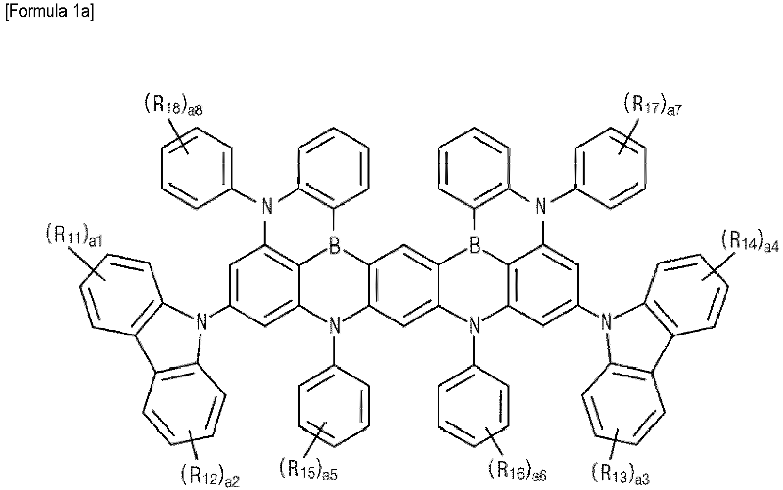
- In Formula 1a, each of R11, R12, R13, R14, R15, R16, R17 and R18 is independently selected from the group consisting of deuterium, a substituted or unsubstituted C1 to C10 alkyl group and a substituted or unsubstituted C6 to C30 aryl group. Each of a1, a2, a3 and n4 is independently an integer of 0 to 4, and each of a5, a6, a7 and a8 is independently an integer of 0 to 5.
- For example, in Formula 1a, each of R11, R12, R13, R14, R15, R16, R17 and R18 may be independently selected from a substituted or unsubstituted C1 to C10 alkyl group, e.g., methyl or tert-butyl, each of a1, a2, a3, a4, a5 and a6 may be independently 0 or 1, and each of a7 and a8 may be 0.
- The
first compound 362 inFormula 1 may be one of the compounds in Formula 2.
- The
second compound 364 is represented by Formula 3.

- In Formula 3, each of R21, R22 and R23 is independently selected from the group consisting of a substituted or unsubstituted C1 to C10 alkyl group, a substituted or unsubstituted C6 to C30 aryl group and a substituted or unsubstituted C5 to 30 heteroaryl group. b1 is an integer of 0 to 2, b2 is an integer of 0 to 4, and b3 is an integer of 0 to 3. R24 is selected from the group consisting of absent, hydrogen, a substituted or unsubstituted C1 to C10 alkyl group, a substituted or unsubstituted C6 to C30 aryl group and a substituted or unsubstituted C5 to 30 heteroaryl group. R24 may be selected from the group consisting of hydrogen, a substituted or unsubstituted C1 to C10 alkyl group, a substituted or unsubstituted C6 to C30 aryl group and a substituted or unsubstituted C5 to 30 heteroaryl group.
- For example, in Formula 3, each of R22, R23 and R24 may be independently selected from a substituted or unsubstituted C1 to C10 alkyl group, e.g., methyl or tert-butyl, b2 and b3 may be 1, and b1 may be 0.
- The
second compound 364 may be one of the compounds in Formula 4.

- The
third compound 366 may be represented by Formula 5.
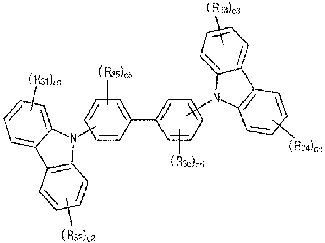
- In Formula 5, each of R31, R32, R33, R34, R35 and R36 is independently selected from the group consisting of a substituted or unsubstituted C1 to C10 alkyl group, a substituted or unsubstituted C6 to C30 aryl group and a substituted or unsubstituted C5 to C30 heteroaryl group, and each of c1, c2, c3, c4, c5 and c6 is independently an integer of 0 to 4.
- For example, each of R31, R32, R33 and R34 may be independently selected from a substituted or unsubstituted C1 to C10 alkyl group, e.g., methyl or tert-butyl and a substituted or unsubstituted C6 to C30 aryl group, e.g., phenyl unsubstituted or substituted with a C1 to C10 alkyl group, e.g., methyl, each of c1, c2, c3 and c4 may be independently 0 or 1, and c5 and c6 may be 0.
- In Formula 5, a linking position of the carbazole moiety may be specified. Namely, Formula 5 may be represented by Formula 5a.

- In Formula 5a, the definition of each of R31, R32, R33, R34, R35, R36, c1, c2, c3, c4, c5 and c6 is same as those in Formula 5.
- For example, the
third compound 366 may be one of the compounds in Formula 6.

- The
fourth compound 368 is represented by Formula 7.

- In Formula 7, each of R41, R42, R43 and R44 is independently selected from the group consisting of a substituted or unsubstituted C1 to C10 alkyl group, a substituted or unsubstituted C6 to C30 aryl group and a substituted or unsubstituted C5 to 30 heteroaryl group, and each of d1, d2, d3 and d4 is independently an integer of 0 to 4.
- For example, each of R41, R42, R43 and R44 may be independently selected from a C1 to C10 alkyl group, e.g., methyl or tert-butyl, and a C6 to C30 aryl group, e.g., phenyl, unsubstituted or substituted with a C1 to C10 alkyl group, e.g., tert-butyl, and each of d1, d2, d3 and d4 may be independently 0 or 1.
- The
fourth compound 368 may be one of the compounds in Formula 8.
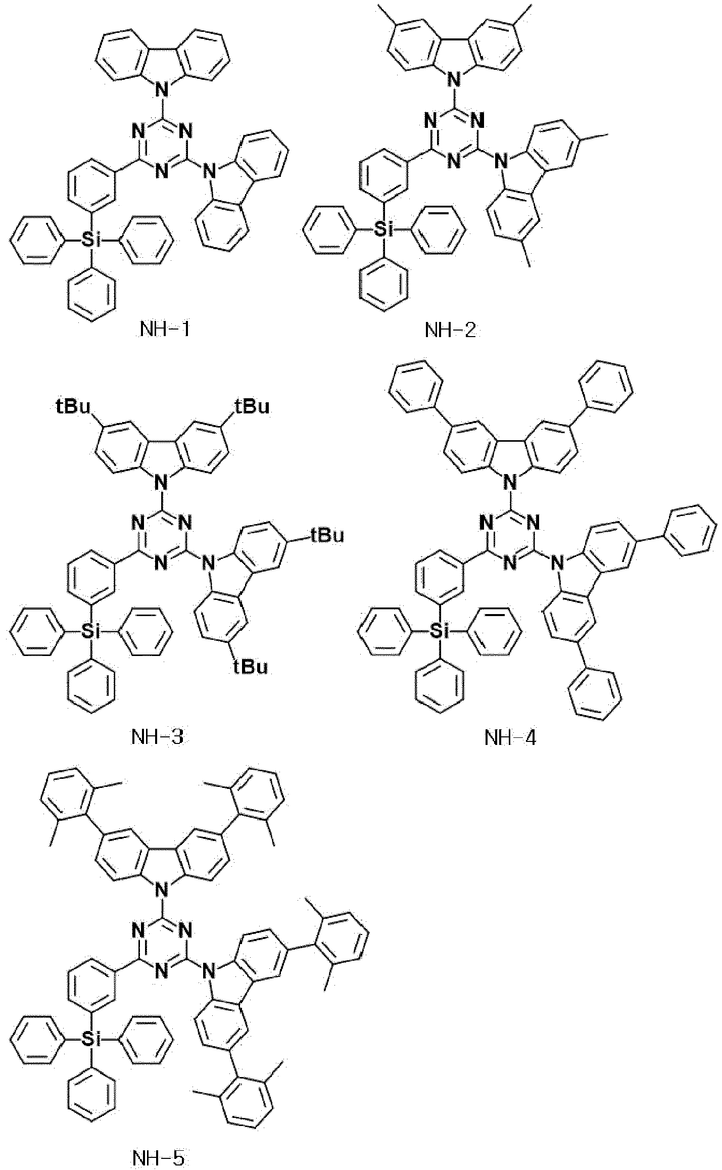
- The second
blue EML 360 being the PSF emitting layer consists of the first tofourth compounds first compound 362, a weight % of thesecond compound 364, a weight % of thethird compound 366 and a weight % of thefourth compound 368 in the secondblue EML 360 is 100 wt%. - In the second
blue EML 360, the weight % of thesecond compound 364 is greater than that of thefirst compound 362 and is smaller than each of the weight % of thethird compound 366 and the weight % of thefourth compound 368. The weight % of thethird compound 366 and the weight % of thefourth compound 368 may be same or different. For example, in the secondblue EML 360, with respect to thefirst compound 362, thesecond compound 364 may have a weight % of about 500 to 2000, and each of the third andfourth compounds - In the second
blue EML 360, a difference" I λmax(FD1_Abs)-λmax(PD_PL) I " between a maximum absorption wavelength "λmax(FD1_Abs)" of thefirst compound 362 "FD1" and a maximum emission wavelength "λmax(PD_PL)" of thesecond compound 364 "PD" is 10nm or less. As a result, the emission property of the OLED D1-B is significantly improved. - The first
blue EML 320 being the fluorescent emitting layer includes afifth compound 322 and asixth compound 324. Thefifth compound 322 is a fluorescent compound, e.g., a fluorescent emitter or a fluorescent dopant, and thesixth compound 324 is a host. - The
fifth compound 322 is represented by Formula 9.
- In Formula 9, each of Ar1, Ar2, Ar3 and Ar4 is independently selected from the group consisting of a substituted or unsubstituted C1 to C10 alkyl group, a substituted or unsubstituted C6 to C30 aryl group and a substituted or unsubstituted C6 to C30 arylamine (arylamino) group.
- For example, each of Ar1, Ar2, Ar3 and Ar4 may be independently selected from a C1 to C10 alkyl group, e.g., tert-butyl, and a C6 to C30 aryl group, e.g., phenyl or naphthyl.
- The
fifth compound 322 may be one of the compounds in Formula 10.

- The
sixth compound 324 is represented by Formula 5. Thesixth compound 324 and thethird compound 366 may be different. - In Formula 5, a linking position of the carbazole moiety may be specified. Namely, the
sixth compound 324 may be represented by Formula 11.
- In Formula 11, each of R51, R52, R53, R54, R55 and R56 is independently selected from the group consisting of a substituted or unsubstituted C1 to C10 alkyl group, a substituted or unsubstituted C6 to C30 aryl group and a substituted or unsubstituted C5 to C30 heteroaryl group, and each of e1, e2, e3, e4, e5 and e6 is independently an integer of 0 to 4.
- For example, each of R51, R52, R53, R54, R55 and R56 may be independently selected from a substituted or unsubstituted C1 to C10 alkyl group, e.g., methyl or tert-butyl and a substituted or unsubstituted C6 to C30 aryl group, e.g., phenyl unsubstituted or substituted with a C1 to C10 alkyl group, e.g., methyl, and each of e1, e2, e3, e4, e5 and e6 may be independently 0 or 1.
- For example, the
sixth compound 324 may be one of the compounds inFormula 12.
- In the blue OLED D1-B, the second
blue EML 360 being the PSF emitting layer is disposed to be closer to thesecond electrode 230 being the transparent electrode. Namely, the secondblue EML 360 being the PSF emitting layer is positioned between thesecond electrode 230 being the transparent electrode and the firstblue EML 320 being the fluorescent emitting layer. - The first
blue EML 320 being the fluorescent emitting layer consists of the fifth andsixth compounds fifth compound 322 and a weight % of thesixth compound 324 in the firstblue EML 320 is 100 wt%. - In the first
blue EML 320, the weight % of the fifth compound 233 is smaller than that of thesixth compound 324. For example, in the firstblue EML 320, thefifth compound 322 may have a weight % of 0.1 to 10. - A difference" | I2nd(EML2)-I2nd(EML1) | " between a second emission peak intensity "I2nd(EML2)" of the second
blue EML 360 being the PSF emitting layer and a second emission peak intensity "I2nd(EML1)" of the firstblue EML 320 being the fluorescent emitting layer is 0.1 or less. As a result, strong cavity effect is provided in the blue OLED D1-B so that the blue OLED D1-B has lower driving voltage and significantly improved blue emitting efficiency. - In addition, a difference" I Amax(FD2_PL)-Amax(FD1_PL) I " between a maximum emission wavelength "Amax(FD2_PL)" of the
fifth compound 322 "FD2" in the firstblue EML 320 being the fluorescent emitting layer and a maximum emission wavelength "Amax(FD1_PL)" of thefirst compound 362 "FD1" in the secondblue EML 360 being the PSF emitting layer is 15nm or less. As a result, the emitting property of the blue OLED D1-B is further improved. - In the specification, "the second emission peak" means that an emission peak having a second greatest intensity or an emission peak at an emission wavelength obtained by adding 30 nm to the maximum emission wavelength.
- The first
blue EML 320 has a first thickness t1, and the secondblue EML 360 has a second thickness t2 being greater than the first thickness t1. For example, the first thickness t1 may have a range of 15 to 30nm, and the second thickness t2 may have a range of 25 to 40nm. - In the blue OLED D1-B, in which the
first electrode 210 is a transparent electrode and thesecond electrode 230 is a reflective electrode, the second emittingpart 350 including the secondblue EML 360 being the PSF emitting layer is disposed to be closer to thefirst electrode 210. Namely, the second emittingpart 350 including the secondblue EML 360 being the PSF emitting layer is positioned between thefirst electrode 210 and the first emittingpart 310 including the firstblue EML 320 being the fluorescent emitting layer. - The first
red EML 620 being the fluorescent emitting layer includes aseventh compound 622, aneighth compound 624 and aninth compound 626. Theseventh compound 622 is a fluorescent compound, e.g., a fluorescent emitter or a fluorescent dopant, the eighth compound 524 is a delayed fluorescent compound, e.g., an auxiliary dopant or an auxiliary host, and theninth compound 626 is a host. - The second
red EML 660 being the phosphorescent emitting layer includes atenth compound 662 and aneleventh compound 664. Thetenth compound 662 is a phosphorescent compound, e.g., a phosphorescent emitter or a phosphorescent dopant, and theeleventh compound 664 is a host. - In the red OLED D1-R, the second
red EML 660 being the phosphorescent emitting layer is disposed to be closer to thesecond electrode 230 being the transparent electrode. Namely, the secondred EML 660 being the phosphorescent emitting layer is positioned between thesecond electrode 230 being the transparent electrode and the firstred EML 620 being the fluorescent emitting layer. Since the secondred EML 660 being the phosphorescent emitting layer, which has higher emitting efficiency (cd/A) than the firstred EML 620 being the fluorescent emitting layer, is disposed to be closer to thesecond electrode 230 being the transparent electrode, the emitting property of the red OLED D1-R is improved. For example, a quantum efficiency of thetenth compound 662 in the secondred EML 660 may be greater than that of theseventh compound 622 in the firstred EML 620. - The first
green EML 720 being the phosphorescent emitting layer includes atwelfth compound 722 and athirteenth compound 724. Thetwelfth compound 722 is a phosphorescent compound, e.g., a phosphorescent emitter or a phosphorescent dopant, and thethirteenth compound 724 is a host. - The second
green EML 760 being the fluorescent emitting layer includes afourteenth compound 762, afifteenth compound 764 and asixteenth compound 766. Thefourteenth compound 762 is a fluorescent compound e.g., a fluorescent emitter or a fluorescent dopant, thefifteenth compound 764 is a delayed fluorescence compound e.g., an auxiliary dopant or an auxiliary host, and thesixteenth compound 766 is a host. - In the red OLED D1-R, in which the
first electrode 210 is a transparent electrode and thesecond electrode 230 is a reflective electrode, the second emittingpart 650 including the secondred EML 660 being the phosphorescent emitting layer is disposed to be closer to thefirst electrode 210 being the transparent electrode. Namely, the second emittingpart 650 including the secondred EML 660 being the phosphorescent emitting layer is positioned between thefirst electrode 210 being the transparent electrode and the first emittingpart 610 including the firstred EML 620 being the fluorescent emitting layer. - In the green OLED D1-G, the second
green EML 760 being the fluorescent emitting layer is disposed to be closer to thesecond electrode 230 being the transparent electrode. Namely, the secondgreen EML 760 being the fluorescent emitting layer is positioned between thesecond electrode 230 being the transparent electrode and the firstgreen EML 720 being the phosphorescent emitting layer. Since the secondgreen EML 760 being the fluorescent emitting layer, which has higher emitting efficiency (cd/A) than the firstgreen EML 720 being the phosphorescent emitting layer, is disposed to be closer to thesecond electrode 230 being the transparent electrode, the emitting property of the green OLED D1-G is improved. For example, a quantum efficiency of thefifteenth compound 762 in the secondgreen EML 760 may be greater than that of thetwelfth compound 722 in the firstgreen EML 720. - In the green OLED D1-R, in which the
first electrode 210 is a transparent electrode and thesecond electrode 230 is a reflective electrode, the second emittingpart 750 including the secondgreen EML 760 being the fluorescent emitting layer is disposed to be closer to thefirst electrode 210 being the transparent electrode. Namely, the second emittingpart 750 including the secondgreen EML 760 being the fluorescent emitting layer is positioned between thefirst electrode 210 being the transparent electrode and the first emittingpart 710 including the firstgreen EML 720 being the phosphorescent emitting layer. - The
seventh compound 622 in the firstred EML 620 may be represented by Formula 13.
- In Formula 13, each of R61 and R62 is independently selected from the group consisting of hydrogen and a substituted or unsubstituted C6 to C30 aryl group. Each of R63 and R64 is independently selected from the group consisting of hydrogen, a substituted or unsubstituted C1 to C10 alkyl group and a substituted or unsubstituted C6 to C30 aryl group, or R63 and R64 are connected to each other to form a substituted or unsubstituted aromatic ring or a substituted or unsubstituted fused-ring. Each of R65 and R66 is independently selected from the group consisting of hydrogen and a substituted or unsubstituted C6 to C30 aryl group. Each of R67 and R68 is independently selected from the group consisting of hydrogen, a substituted or unsubstituted C1 to C10 alkyl group and a substituted or unsubstituted C6 to C30 aryl group, or R67 and R68 are connected to each other to form a substituted or unsubstituted aromatic ring or a substituted or unsubstituted fused-ring.
- For example, the
seventh compound 622 in the firstred EML 620 may be one of the compounds in Formula 14.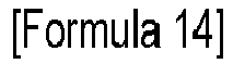

- Each of the
eighth compound 624 in the firstred EML 620 and thefifteenth compound 764 in the secondgreen EML 760 is represented by Formula 15.

- In Formula 15, each of R71 and R72 is independently selected from the group consisting of a substituted or unsubstituted C1 to C10 alkyl group and a substituted or unsubstituted C6 to C30 aryl group, and R73 is selected from the group consisting of hydrogen, a substituted or unsubstituted C1 to C10 alkyl group and a substituted or unsubstituted C6 to C30 aryl group. Each of f1 and f2 is independently an integer of 0 to 5, and f3 is an integer of 1 to 4.
- For example, each of R71 and R72 may be a C1 to C10 alkyl group, e.g., methyl or tert-butyl, and each of f1 and f2 may be independently 0 or 1. R73 may be a C6 to C30 aryl group, e.g., phenyl, unsubstituted or substituted with a C1 to C10 alkyl group, e.g., methyl, and f3 may be 1.
- The
eighth compound 624 in the firstred EML 620 and thefifteenth compound 764 in the secondgreen EML 760 may be same or different. For example, each of theeighth compound 624 in the firstred EML 620 and the fifteenth compound 764in the secondgreen EML 760 may be independently selected from the compounds in Formula 16.

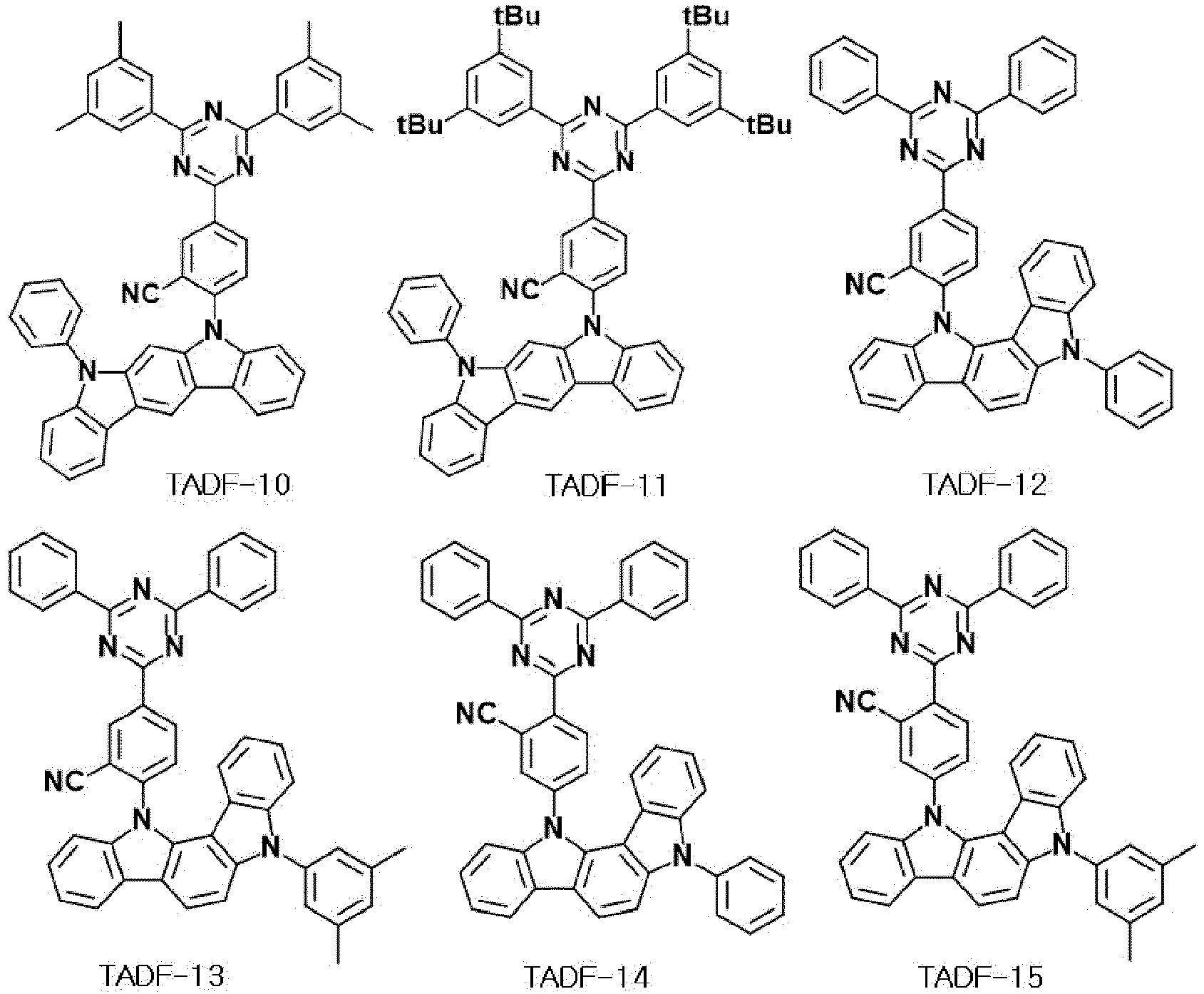
- The
tenth compound 662 in the secondred EML 660 is one of the compounds in Formula 17.
- The
twelfth compound 722 in the firstgreen EML 720 is one of the compounds in Formula 18.

- The
fourteenth compound 762 in the secondgreen EML 760 is represented by Formula 19.
- In Formula 19, X1 is O or S. Each of R81 and R82 is independently selected from the group consisting of hydrogen, a substituted or unsubstituted C1 to C10 alkyl group and a substituted or unsubstituted C6 to C30 aryl group, or R81 and R82 are connected to each other to form a substituted or unsubstituted aromatic ring. Each of R83 and R84 is independently selected from the group consisting of hydrogen, a substituted or unsubstituted C1 to C10 alkyl group and a substituted or unsubstituted C6 to C30 aryl group, or R83 and R84 are connected to each other to form a substituted or unsubstituted aromatic ring.
- For example, the
fourteenth compound 762 in the secondgreen EML 760 may be one of the compounds in Formula 20.

- Each of the
ninth compound 626 in the firstred EML 620 and theeleventh compound 664 in the secondred EML 660 is represented by Formula 21.
- In Formula 21, each of R91, R92, R93 and R94 is independently selected from the group consisting of a substituted or unsubstituted C1 to C10 alkyl group and a substituted or unsubstituted C6 to C30 aryl group, and each of g1, g2, g3 and g4 is independently an integer of 0 to 4. Y1 is represented by Formula 21a or Formula 21b.


- In Formula 21a, each of R95 and R96 is independently selected from the group consisting of a substituted or unsubstituted C1 to C10 alkyl group and a substituted or unsubstituted C6 to C30 aryl group, and each of g5 and g6 is independently an integer of 0 to 4.
- In Formula 21b, each of R97 and R98 is independently selected from the group consisting of a substituted or unsubstituted C1 to C10 alkyl group and a substituted or unsubstituted C6 to C30 aryl group, g7 is an integer of 0 to 3, and g8 is an integer of 0 to 4. X2 is NR99, O or S, and R99 is selected from the group consisting of hydrogen, a substituted or unsubstituted C1 to C10 alkyl group and a substituted or unsubstituted C6 to C30 aryl group.
- The
ninth compound 626 in the firstred EML 620 and theeleventh compound 664 in the secondred EML 660 may be same or different. - Each of the
ninth compound 626 in the firstred EML 620 and theeleventh compound 664 in the secondred EML 660 may be independently selected from the compounds in Formula 22.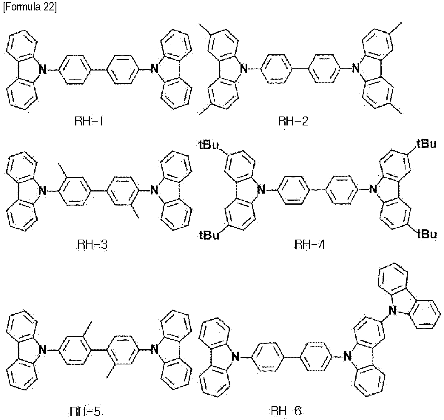

- Each of the
thirteenth compound 724 in the firstgreen EML 720 and thesixteenth compound 766 in the secondgreen EML 760 is represented by Formula 23.

- In Formula 23, each of R101 and R102 is independently selected from the group consisting of a substituted or unsubstituted C1 to C10 alkyl group and a substituted or unsubstituted C6 to C30 aryl group. Each of R103 and R104 is independently selected from the group consisting of a substituted or unsubstituted C1 to C10 alkyl group and a substituted or unsubstituted C6 to C30 aryl group, or R103 and R104 are connected to each other to form a substituted or unsubstituted hetero ring. Each of h1, h2, h3 and h4 is independently an integer of 0 to 4, and Y2 is represented by Formula 23a or Formula 23b.


- In Formula 23a, each of R105 and R106 is independently selected from the group consisting of a substituted or unsubstituted C1 to C10 alkyl group and a substituted or unsubstituted C6 to C30 aryl group, and each of h5 and h6 is independently an integer of 0 to 4.
- In Formula 23b, each of R107 and R108 is independently selected from the group consisting of a substituted or unsubstituted C1 to C10 alkyl group and a substituted or unsubstituted C6 to C30 aryl group, h7 is an integer of 0 to 3, and h8 is an integer of 0 to 4. X3 is NR109, O or S, and R109 is selected from the group consisting of hydrogen, a substituted or unsubstituted C1 to C10 alkyl group and a substituted or unsubstituted C6 to C30 aryl group.
- The
thirteenth compound 724 in the firstgreen EML 720 and thesixteenth compound 766 in the secondgreen EML 760 may be same or different. In addition, thethirteenth compound 724 in the firstgreen EML 720 and thesixteenth compound 766 in the secondgreen EML 760 may be same as or different from thesixth compound 324 in the firstblue EML 320. - Each of the
thirteenth compound 724 in the firstgreen EML 720 and thesixteenth compound 766 in the secondgreen EML 760 may be independently selected from the compounds in Formula 24.

- The first
red EML 620 in the red OLED D1-R consists of the seventh toninth compounds seventh compound 622, a weight % of theeighth compound 624 and a weight % ofninth compound 626 in the firstred EML 620 is 100wt%. - In the first
red EML 620 of the red OLED D1-R, the weight % of theeighth compound 624 is greater than that of theseventh compound 622 and is equal to or smaller than that of theninth compound 626. For example, in the firstred EML 620, with respect to theseventh compound 622, each of theeighth compound 624 theninth compound 626 may have a weight % of about 4000 to 6000. - The second
red EML 660 in the red OLED D1-R consists of the tenth andeleventh compounds tenth compound 664 and a weight % of theeleventh compound 664 in the secondred EML 660 is 100wt%. - In the second
red EML 660 of the red OLED D1-R, the weight % of theeleventh compound 664 is greater than that of thetenth compound 662. For example, in the secondred EML 660, thetenth compound 662 may have a weight % of about 0.1 to 10. - The first
red EML 620 may have the same thickness as the firstblue EML 320, and the secondred EML 660 may have the same thickness as the secondblue EML 360. Namely, the secondred EML 660 may have a thickness being greater than the firstred EML 620. For example, the firstred EML 620 may have a thickness with a range of 15 to 30nm, and the secondred EML 660 may have a thickness with a range of 25 to 40nm. - The first
green EML 720 in the green OLED D1-G consists of the twelfth andthirteenth compounds twelfth compound 724 and a weight % of thethirteenth compound 724 in the firstgreen EML 720 is 100wt%. - In the first
green EML 720 of the green OLED D1-G, the weight % of thethirteenth compound 724 is greater than that of thetwelfth compound 722. For example, in the firstgreen EML 720, thetwelfth compound 722 may have a weight % of about 0.1 to 15. - The second
green EML 760 in the green OLED D1-G consists of the fourteenth tosixteenth compounds fourteenth compound 762, a weight % of thefifteenth compound 764 and a weight % ofsixteenth compound 766 in the secondgreen EML 760 is 100wt%. - In the second
green EML 760 of the green OLED D1-G, the weight % of thefifteenth compound 764 is greater than that of thefourteenth compound 762 and is equal to or smaller than that of thesixteenth compound 766. For example, in the secondgreen EML 760, with respect to thefourteenth compound 762, each of thefifteenth compound 764 thesixteenth compound 766 may have a weight % of about 4000 to 6000. - The first
green EML 720 may have the same thickness as the firstblue EML 320, and the secondgreen EML 760 may have the same thickness as the secondblue EML 360. Namely, the secondgreen EML 760 may have a thickness being greater than the firstgreen EML 720. For example, the firstgreen EML 720 may have a thickness with a range of 15 to 30nm, and the secondgreen EML 760 may have a thickness with a range of 25 to 40nm. - Each of the
HILs 
- Alternatively, each of the HILs 311, 611 and 711 may include one of the compounds selected from the group consisting of 4,4',4"-tris(3-methylphenylamino)triphenylamine (MTDATA), 4,4',4"-tris(N,N-diphenyl-amino)triphenylamine (NATA), 4,4',4"-tris(N-(naphthalene-1-yl)-N-phenyl-amino)triphenylamine (1T-NATA), 4,4',4"-tris(N-(naphthalene-2-yl)-N-phenyl-amino)triphenylamine (2T-NATA), copper phthalocyanine (CuPc), tris(4-carbazoyl-9-yl-phenyl)amine (TCTA), N,N'-diphenyl-N,N'-bis(1-naphthyl)-1,1'-biphenyl-4,4"-diamine (NPB or NPD), 1,4,5,8,9,11-hexaazatriphenylenehexacarbonitrile(dipyrazino[2,3-f:2'3'-h]quinoxaline-2,3,6,7,10,11-hexacarbonitrile (HAT-CN), 1,3,5-tris[4-(diphenylamino)phenyl]benzene (TDAPB), poly(3,4-ethylenedioxythiphene)polystyrene sulfonate (PEDOT/PSS) and N-(biphenyl-4-yl)-9,9-dimethyl-N-(4-(9-phenyl-9H-carbazol-3-yl)phenyl)-9H-fluoren-2-amine. Each of the
HILs - Each of the
first HTLs second HTLs 
- Alternatively, each of the first HTLs 313, 613 and 713 and the second HTLs 351, 651 and 751 may include one of the compounds selected from the group consisting of N,N'-diphenyl-N,N'-bis(3-methylphenyl)-1,1'-biphenyl-4,4'-diamine (TPD), NPB (or NPD), 4,4'-bis(N-carbazolyl)-1,1'-biphenyl (CBP), poly[N,N'-bis(4-butylphenyl)-N,N'-bis(phenyl)-benzidine] (Poly-TPD), (poly[(9,9-dioctylfluorenyl-2,7-diyl)-co-(4,4'-(N-(4-sec-butylphenyl)diphenylamine))] (TFB), di-[4-(N,N-di-p-tolyl-amino)-phenyl]cyclohexane (TAPC), 3,5-di(9H-carbazol-9-yl)-N,N-diphenylaniline (DCDPA), N-(biphenyl-4-yl)-9,9-dimethyl-N-(4-(9-phenyl-9H-carbazol-3-yl)phenyl)-9H-fluoren-2-amine and N-(biphenyl-4-yl)-N-(4-(9-phenyl-9H-carbazol-3-yl)phenyl)biphenyl-4-amine.
- Each of the
first HTLs second HTLs first HTLs second HTLs - Each of the
first ETLs second ETLs 
- Alternatively, each of the first ETLs 319, 619 and 719 and the second ETLs 357, 657 and 757 may include one of the compounds selected from the group consisting of tris-(8-hydroxyquinoline aluminum (Alq3), 2-biphenyl-4-yl-5-(4-t-butylphenyl)-1,3,4-oxadiazole (PBD), spiro-PBD, lithium quinolate (Liq), 1,3,5-tris(N-phenylbenzimidazol-2-yl)benzene (TPBi), bis(2-methyl-8-quinolinolato-N1,O8)-(1,1'-biphenyl-4-olato)aluminum(BAIq), 4,7-diphenyl-1,10-phenanthroline (Bphen), 2,9-bis(naphthalene-2-yl)4,7-diphenyl-1,10-phenanthroline (NBphen), 2,9-dimethyl-4,7-diphenyl-1,10-phenathroline (BCP), 3-(4-biphenyl)-4-phenyl-5-tert-butylphenyl-1,2,4-triazole (TAZ), 4-(naphthalen-1-yl)-3,5-diphenyl-4H-1,2,4-triazole(NTAZ), 1,3,5-tri(p-pyrid-3-yl-phenyl)benzene (TpPyPB), 2,4,6-tris(3'-(pyridin-3-yl)biphenyl-3-yl)1,3,5-triazine (TmPPPyTz), poly[9,9-bis(3'-((N,N-dimethyl)-N-ethylammonium)-propyl)-2,7-fluorene]-alt-2,7-(9,9-dioctylfluorene)] (PFNBr), tris(phenylquinoxaline (TPQ) and diphenyl-4-triphenylsilyl-phenylphosphine oxide (TSPO1).
- Each of the
first ETLs second ETLs first ETLs second ETLs - Each of the
EILs 
- Alternatively, each of the
EILs EILs - Each of the
first EBLs second EBLs 

- Alternatively, each of the
first EBLs second EBLs - Each of the
first EBLs second EBLs first EBLs second EBLs - Each of the
first HBLs second HBLs 
- Alternatively, each of the
first HBLs second HBLs - Each of the
first HBLs second HBLs first HBLs second HBLs - Each of the n-
type CGLs ETLs - Each of the p-
type CGLs HTLs - Each of the n-
type CGLs type CGLs type CGLs type CGLs - The
capping layer 290 is positioned on or over thesecond electrode 230 being the transparent electrode. For example, thecapping layer 290 may include the material of theHTLs - As illustrated above, the blue OLED D1-B includes the first emitting
part 310 including a fluorescent emitting layer and the second emittingpart 350 including a PSF emitting layer, and the second emittingpart 350 is disposed to be closer to the transparent electrode. In this instance, a difference" | I2nd(EML2)-I2nd(EML1) | " between a second emission peak intensity of the secondblue EML 360 being the PSF emitting layer and a second emission peak intensity of the firstblue EML 320 being the fluorescent emitting layer is 0.1 or less. As result, strong cavity effect is provided in the blue OLED D1-B so that the blue OLED D1-B has lower driving voltage and significantly-improved blue emitting efficiency. - In addition, the second
blue EML 360 being the PSF emitting layer has higher emitting efficiency than the firstblue EML 320 being the fluorescent emitting layer so that the cavity effect in the blue OLED D1-B is further strengthened. - Moreover, a difference" I Amax(FD2_PL)-Amax(FD1_PL) I " between a maximum emission wavelength "Amax(FD2_PL)" of the
fifth compound 322 "FD2" in the firstblue EML 320 being the fluorescent emitting layer and a maximum emission wavelength "Amax(FD1_PL)" of thefirst compound 362 "FD1" in the secondblue EML 360 being the PSF emitting layer is 15nm or less. As a result, the emitting property of the blue OLED D1-B is further improved. - Furthermore, in the second
blue EML 360 being the PSF emitting layer, a difference" | Amax(FD1_Abs)-λmax(PD_PL) | " between a maximum absorption wavelength "λmax(FD1_Abs)" of thefirst compound 362 "FD1" and a maximum emission wavelength "λmax(PD_PL)" of thesecond compound 364 "PD" is 10nm or less. As a result, the emitting property of the blue OLED D1-B is significantly improved. - Accordingly, the display performance of the organic light emitting display device including the blue OLED D1-B is improved.
- The red OLED D1-R includes the first emitting
part 610 including a fluorescent emitting layer and the second emittingpart 650 including a phosphorescent emitting layer, which has a higher emitting efficiency than the fluorescent emitting layer in the first emittingpart 610, and the second emittingpart 650 is disposed to be closer to the transparent electrode. As a result, strong cavity effect is provided in the red OLED D1-R so that the red OLED D1-R has low driving voltage and significantly-improved red emitting efficiency. - The green OLED D1-G includes the first emitting
part 710 including a phosphorescent emitting layer and the second emittingpart 750 including a fluorescent emitting layer, which has a higher emitting efficiency than the phosphorescent emitting layer in the first emittingpart 710, and the second emittingpart 750 is disposed to be closer to the transparent electrode. As a result, strong cavity effect is provided in the green OLED D1-G so that the green OLED D1-G has low driving voltage and significantly-improved red emitting efficiency. - Accordingly, the display performance of the organic light emitting display device including the blue OLED D1-B, the red OLED D1-R and the green OLED D1-G is improved.
-
FIG. 8 is a schematic cross-sectional view of an organic light emitting display device according to a fourth embodiment of the present disclosure, andFIG. 9 is a schematic cross-sectional view of a white OLED of the present disclosure. - As shown in
FIG. 8 , the organic light emittingdisplay device 800 includes afirst substrate 810, where a red pixel region RP, a green pixel region GP and a blue pixel region BP are defined, asecond substrate 870 facing thefirst substrate 810, an OLED D, which is positioned between the first andsecond substrates color filter layer 880 between the OLED D and thesecond substrate 870. - Each of the first and
second substrates second substrates - A
buffer layer 820 is formed on the substrate, and the TFT Tr corresponding to each of the red, green and blue pixel regions RP, GP and BP is formed on thebuffer layer 820. Thebuffer layer 820 may be omitted. - A
semiconductor layer 822 is formed on thebuffer layer 820. Thesemiconductor layer 822 may include an oxide semiconductor material or polycrystalline silicon. - A
gate insulating layer 824 is formed on thesemiconductor layer 822. Thegate insulating layer 824 may be formed of an inorganic insulating material such as silicon oxide or silicon nitride. - A
gate electrode 830, which is formed of a conductive material, e.g., metal, is formed on thegate insulating layer 824 to correspond to a center of thesemiconductor layer 822. - An interlayer insulating
layer 832, which is formed of an insulating material, is formed on thegate electrode 830. The interlayer insulatinglayer 832 may be formed of an inorganic insulating material, e.g., silicon oxide or silicon nitride, or an organic insulating material, e.g., benzocyclobutene or photo-acryl. - The interlayer insulating
layer 832 includes first and second contact holes 834 and 836 exposing both sides of thesemiconductor layer 822. The first and second contact holes 834 and 836 are positioned at both sides of thegate electrode 830 to be spaced apart from thegate electrode 830. - A
source electrode 840 and adrain electrode 842, which are formed of a conductive material, e.g., metal, are formed on theinterlayer insulating layer 832. - The
source electrode 840 and thedrain electrode 842 are spaced apart from each other with respect to thegate electrode 830 and respectively contact both sides of thesemiconductor layer 822 through the first and second contact holes 834 and 836. - The
semiconductor layer 822, thegate electrode 830, thesource electrode 840 and thedrain electrode 842 constitute the TFT Tr. The TFT Tr serves as a driving element. Namely, the TFT Tr may correspond to the driving TFT Td (ofFIG. 1 ). - Although not shown, the gate line and the data line cross each other to define the pixel region, and the switching TFT is formed to be connected to the gate and data lines. The switching TFT is connected to the TFT Tr as the driving element.
- In addition, the power line, which may be formed to be parallel to and spaced apart from one of the gate and data lines, and the storage capacitor for maintaining the voltage of the gate electrode of the TFT Tr in one frame may be further formed.
- A
planarization layer 850, which includes adrain contact hole 852 exposing thedrain electrode 842 of the TFT Tr, is formed to cover the TFT Tr. - A
first electrode 810, which is connected to thedrain electrode 842 of the TFT Tr through thedrain contact hole 852, is separately formed in each pixel region and on theplanarization layer 850. Thefirst electrode 810 may be an anode and may include a transparent conductive oxide material layer, which is formed of a conductive material, e.g., a transparent conductive oxide (TCO), having a relatively high work function and a reflective layer. Namely, thefirst electrode 810 is a reflective electrode. - Alternatively, the
first electrode 810 may have a single-layered structure of transparent conductive oxide material layer. Namely, thefirst electrode 810 may a transparent electrode. - For example, the transparent conductive oxide material layer of the
first electrode 810 may be formed of one of indium-tin-oxide (ITO), indium-zinc-oxide (IZO), indium-tin-zinc-oxide (ITZO), tin oxide (SnO), zinc oxide (ZnO), indium-copper-oxide (ICO) and aluminum-zinc-oxide (AI:ZnO, AZO), and the reflective layer of thefirst electrode 810 may be formed of one of silver (Ag), an alloy of Ag and one of palladium (Pd), copper (Cu), indium (In) and neodymium (Nd), and aluminum-palladium-copper (APC) alloy. For example, thefirst electrode 810 may have a structure of ITO/Ag/ITO or ITO/APC/ITO. - A bank layer 866 is formed on the
planarization layer 850 to cover an edge of thefirst electrode 810. Namely, the bank layer 866 is positioned at a boundary of the pixel region and exposes a center of thefirst electrode 810 in each of the red, green and blue pixel regions RP, GP and BP. The bank layer 866 may be omitted. - An organic
light emitting layer 820 is formed on thefirst electrode 810, and thesecond electrode 830 is formed over thesubstrate 810 including the organiclight emitting layer 820. - In the organic light emitting
display device 800, since the light emitted from the organiclight emitting layer 820 is incident to thecolor filter layer 880 through thesecond electrode 830, thesecond electrode 830 has a thin profile for transmitting the light. - The
second electrode 830 covers an entire surface of the display area and may be formed of a conductive material having a relatively low work function to serve as a cathode. For example, thesecond electrode 830 may be formed of aluminum (Al), magnesium (Mg), calcium (Ca), silver (Ag) or their alloy, e.g., Mg-Ag alloy (MgAg). Thesecond electrode 830 may have a thin profile, e.g., 10 to 30nm, to be transparent (or semi-transparent). - The
first electrode 810, the organic emittinglayer 820 and thesecond electrode 830 constitute the OLED D. The OLED D may further include a capping layer 890 (ofFIG. 9 ) for enhancing the light extraction. - Referring to
FIG. 9 , the organiclight emitting layer 820 includes a first emittingpart 710 including a firstblue EML 720, which is a fluorescent emitting layer, a second emittingpart 730 including a secondblue EML 740, which is a PSF emitting layer, and a third emittingpart 750 including athird EML 760, which emits red light and yellow-green light. It will be appreciated, that thethird EML 760 may comprise sublayers, a sublayer emitting red light and a sublayer emitting yellow-green light In addition, the organiclight emitting layer 820 may further include afirst CGL 770 between the first and third emittingparts second CGL 780 between the second and third emittingparts - The organic light emitting
display device 800 includes the red, green and blue pixel regions RP, GP and BP, and the OLED D2 emits white light in the red, green and blue pixel regions RP, GP and BP. - The first emitting
part 710 may further include at least one of afirst HTL 714 under the firstblue EML 720 and afirst ETL 716 on the firstblue EML 720. In addition, the first emittingpart 710 may further include anHIL 712 under thefirst HTL 714. - Although not shown, the first emitting
part 710 may further include at least one of a first EBL between the firstblue EML 720 and thefirst HTL 714 and a first HBL between the firstblue EML 720 and thefirst ETL 716. - The second emitting
part 730 may further include at least one of asecond HTL 732 under the secondblue EML 740 and asecond ETL 734 on the secondblue EML 740. In addition, the second emittingpart 730 may further include anEIL 736 on thesecond ETL 734. - Although not shown, the second emitting
part 730 may further include at least one of a second EBL between the secondblue EML 740 and thesecond HTL 732 and a second HBL between the secondblue EML 740 and thesecond ETL 734. - In the third emitting
part 750, thethird EML 760 may include ared EML 762 and agreen EML 764. Thegreen EML 764 may be positioned between thered EML 762 and the second emittingpart 730. In addition, thethird EML 760 may further include a yellow-green EML between thered EML 762 and thegreen EML 764. - The
red EML 762 may include a red host and a red dopant (emitter), thegreen EML 764 may include a green host and a green dopant, and the yellow-green EML may include a yellow-green host and a yellow-green dopant. Each of the red dopant, the green dopant and the yellow-green dopant may be a fluorescent compound, a phosphorescent compound and a delayed fluorescent compound. - The third
emitting part 750 may further include at least one of athird HTL 752 under thethird EML 760 and athird ETL 754 on thethird EML 760. - Although not shown, the third emitting
part 750 may further include at least one of a third EBL between thethird EML 760 and thethird HTL 752 and a third HBL between thethird EML 760 and thethird ETL 754. - The
first CGL 770 is positioned between the first and third emittingparts second CGL 780 is positioned between the second and third emittingparts part 710, thefirst CGL 770, the third emittingpart 750, thesecond CGL 780 and the second emittingpart 730 are sequentially stacked on thefirst electrode 810. In other words, the first emittingpart 710 is positioned between thefirst electrode 810 and thefirst CGL 770, the third emittingpart 750 is positioned between the first and second CGLs 770 and 780, and the second emittingpart 730 is positioned between thesecond electrode 830 and thesecond CGL 780. - The
first CGL 770 may be a P-N junction CGL of a first N-type CGL 772 and a first P-type CGL 774, and thesecond CGL 780 may be a P-N junction CGL of a second N-type CGL 782 and a second P-type CGL 784. - In the
first CGL 770, the first N-type CGL 772 is positioned between thefirst ETL 716 and thethird HTL 752, and the first P-type CGL 774 is positioned between the first N-type CGL 772 and thethird HTL 752. - In the
second CGL 780, the second N-type CGL 782 is positioned between thethird ETL 754 and thesecond HTL 732, and the second P-type CGL 784 is positioned between the second N-type CGL 782 and thesecond HTL 732. - The second
blue EML 740 includes a first compound 742 represented byFormula 1, a second compound 744 represented by Formula 3, a third compound 746 represented by Formula 5 and a fourth compound 748 represented by Formula 7, and the firstblue EML 720 includes afifth compound 722 represented by Formula 9 and asixth compound 724 represented by Formula 11. - Namely, the first
blue EML 720 is a fluorescent emitting layer, and the secondblue EML 740 is a PSF emitting layer. - A difference" | I2nd(EML2)-I2nd(EML1) | " between a second emission peak intensity of the second
blue EML 740 being the PSF emitting layer and a second emission peak intensity of the firstblue EML 720 being the fluorescent emitting layer is 0.1 or less. As result, strong cavity effect is provided in the OLED D2 so that the OLED D2 has lower driving voltage and significantly-improved blue emitting efficiency. - In addition, the second
blue EML 740 being the PSF emitting layer has higher emitting efficiency than the firstblue EML 720 being the fluorescent emitting layer so that the cavity effect in the OLED D2 is further strengthened. - Moreover, a difference" I Amax(FD2_PL)-Amax(FD1_PL) I " between a maximum emission wavelength "Amax(FD2_PL)" of the
fifth compound 722 "FD2" in the firstblue EML 720 being the fluorescent emitting layer and a maximum emission wavelength "Amax(FD1_PL)" of the first compound 742 "FD1" in the secondblue EML 740 being the PSF emitting layer is 15nm or less. As a result, the emitting property of the OLED D2 is further improved. - Furthermore, in the second
blue EML 740 being the PSF emitting layer, a difference" | Amax(FD1_Abs)-λmax(PD_PL) | " between a maximum absorption wavelength "λmax(FD1_Abs)" of the first compound 742 "FD1" and a maximum emission wavelength "λmax(PD_PL)" of the second compound 744 "PD" is 10nm or less. As a result, the emitting property of the OLED D2 is significantly improved. - Referring back to
FIG. 8 , thecolor filter layer 880 is disposed over the OLED D2 and includes ared color filter 882, agreen color filter 884 and ablue color filter 886 respectively corresponding to the red, green and blue pixels RP, GP and BP. - The
red color filter 882 may include at least one of red dye and red pigment, thegreen color filter 884 may include at least one of green dye and green pigment, and theblue color filter 886 may include at least one of blue dye and blue pigment. - Although not shown, the
color filter layer 880 may be attached to the OLED D2 by using an adhesive layer. Alternatively, thecolor filter layer 880 may be formed directly on the OLED D2. - An encapsulation film (not shown) may be formed to prevent penetration of moisture into the OLED D2. For example, the encapsulation film may include a first inorganic insulating layer, an organic insulating layer and a second inorganic insulating layer sequentially stacked, but it is not limited thereto. The encapsulation film may be omitted.
- A polarization plate (not shown) for reducing an ambient light reflection may be attached to an outer side of the
second substrate 870. For example, the polarization plate may be a circular polarization plate. - In the OLED of
FIG. 8 , the light from the OLED D2 passes through thesecond electrode 830, and thecolor filter layer 880 is disposed over the OLED D2. Alternatively, the light from the OLED D2 passes through thefirst electrode 810, and thecolor filter layer 880 may be disposed between the OLED D2 and thefirst substrate 710. In this instance, the second emittingpart 730 including the secondblue EML 740 being the PSF emitting layer is disposed to be closer to thefirst electrode 810, and the first emittingpart 710 including the firstblue EML 720 being the fluorescent emitting layer is disposed between the third emittingpart 750 and thesecond electrode 830. - A color conversion layer (not shown) may be formed between the OLED D2 and the
color filter layer 880. The color conversion layer may include a red color conversion layer, a green color conversion layer and a blue color conversion layer respectively corresponding to the red, green and blue pixels RP, GP and BP. The white light from the OLED D2 is converted into the red light, the green light and the blue light by the red, green and blue color conversion layer, respectively. For example, the color conversion layer may include a quantum dot. - As described above, in the organic light emitting
display device 800, the OLED D2 in the red, green and blue pixels RP, GP and BP emits the white light, and the white light from the OLED D2 passes through thered color filter 882, thegreen color filter 884 and theblue color filter 886. As a result, the red light, the green light and the blue light are provided from the red pixel RP, the green pixel GP and the blue pixel BP, respectively. - In
FIG. 8 , the OLED D2 emitting the white light is used for a display device. Alternatively, the OLED D2 may be formed on an entire surface of a substrate without at least one of the driving element and the color filter layer to be used for a lightening device. The display device and the lightening device each including the OLED D2 of the present disclosure may be referred to as an organic light emitting device. - In the organic light emitting
display device 800, the white OLED D2 is formed in all of the red, green and blue pixel regions RP, GP and BP, and a full color image is provided by using thecolor filter layer 880. - An anode (ITO/Ag/ITO, 10nm), an HIL (the compound in Formula 25, 3nm), a first HTL (the compound in Formula 26, 27nm), a first EBL (the compound in Formula 29, 5nm), a first EML (23nm), a first HBL (the compound in Formula 30, 5nm), a first ETL (the compound in Formula 27, 12nm), an N-type CGL (the compound in Formula 27 and Li (0.5wt% doping), 12nm), a P-type CGL (the compound in Formula 26 and the compound in Formula 25 (20wt% doping), 5nm), a second HTL (the compound in Formula 26, 55nm), a second EBL (the compound in Formula 29, 5nm), a second EML (30nm), a second HBL (the compound in Formula 30, 5nm), a second ETL (the compound in Formula 27, 25nm), an EIL (the compound in Formula 28, 12nm), a cathode (AgMg, 12nm) and a capping layer (the compound in Formula 26, 75nm) are sequentially deposited to form an OLED.
- The compound R-PD-1 (2wt%) in Formula 17 and the compound RH-1 (98wt%) in Formula 22 are used to form the first EML, and the compound R-FD-1 (1wt%) in Formula 14, the compound TADF-1 (49wt%) in Formula 16 and the compound RH-1 (50wt%) in Formula 22 are used to form the second EML.
- The compound R-FD-1 (1wt%) in Formula 14, the compound TADF-1 (49wt%) in Formula 16 and the compound RH-1 (50wt%) in Formula 22 are used to form the first EML, and the compound R-PD-1 (2wt%) in Formula 17 and the compound RH-1 (98wt%) in Formula 22 are used to form the second EML.
- The compound R-PD-1 (2wt%) in Formula 17 and the compound RH-1 (98wt%) in Formula 22 are used to form a film, and the quantum efficiency of the compound R-PD-1 is measured. In addition, the compound R-FD-1 (2wt%) in Formula 14, the compound TADF-1 (49wt%) in Formula 16 and the compound RH-1 (50wt%) in Formula 22 are used to form a film, and the quantum efficiency of the compound R-FD-1 is measured. As a result of the measurement, the red phosphorescent emitting layer has a quantum efficiency of 93.2%, and the red fluorescent emitting layer has a quantum efficiency of 93.0%.
- The compound G-FD-1 (1wt%) in Formula 20, the compound TADF-12 (29wt%) in Formula 16 and the compound GH-11 (70wt%) in Formula 24 are used to form the first EML, and the compound G-PD-1 (8wt%) in Formula 18 and the compound GH-1 (92wt%) in Formula 24 are used to form the second EML.
- The compound G-PD-1 (8wt%) in Formula 18 and the compound GH-1 (92wt%) in Formula 24 are used to form the first EML, and the compound G-FD-1 (1wt%) in Formula 20, the compound TADF-12 (29wt%) in Formula 16 and the compound GH-11 (70wt%) in Formula 24 are used to form the second EML.
- The compound G-PD-1 (8wt%) in Formula 18 and the compound GH-1 (92wt%) in Formula 24 are used to form a film, and the quantum efficiency of the compound G-PD-1 is measured. In addition, the compound G-FD-1 (1wt%) in Formula 20, the compound TADF-12 (29wt%) in Formula 16 and the compound GH-11 (70wt%) in Formula 24 are used to form a film, and the quantum efficiency of the compound G-FD-1 is measured. As a result of the measurement, the green phosphorescent emitting layer had a quantum efficiency of 91.6%, and the green fluorescent emitting layer had a quantum efficiency of 95.2%.
- The compound FD2-1 (1wt%) in Formula 10 and the compound BH-1 (99wt%) in
Formula 12 are used to form the first and second EMLs. - The compound FD1-1 (1wt%) in Formula 2, the compound PD1-5 (12wt%) in Formula 4, the compound PH-1 (43.5wt%) in Formula 6 and the compound NH-1 (43.5wt%) in Formula 8 are used to form the first EML, and the compound FD2-1 (1wt%) in Formula 10 and the compound BH-1 (99wt%) in
Formula 12 are used to form the second EML. - The compound FD2-1 (1wt%) in Formula 10 and the compound BH-1 (99wt%) in
Formula 12 are used to form the first EML, and the compound FD1-1 (1wt%) in Formula 2, the compound PD1-5 (12wt%) in Formula 4, the compound PH-1 (43.5wt%) in Formula 6 and the compound NH-1 (43.5wt%) in Formula 8 are used to form the second EML. - The compound FD2-1 (1wt%) in Formula 10 and the compound BH-1 (99wt%) in
Formula 12 are used to form a film, and the quantum efficiency of the compound FD2-1 is measured. In addition, the compound FD1-1 (1wt%) in Formula 2, the compound PD1-5 (12wt%) in Formula 4, the compound PH-1 (43.5wt%) in Formula 6 and the compound NH-1 (43.5wt%) in Formula 8 are used to form a film, and the quantum efficiency of the compound G-FD-1 is measured. As a result of the measurement, the blue emitting layer has a quantum efficiency of 94.0%, and the blue PSF emitting layer has a quantum efficiency of 98.5%. - The emitting properties, i.e., the driving voltage (V), the color coordinate index (CIE) and the luminance (cd/A), of the red, green and blue OLEDs in Comparative Examples 1 to 4 and Examples 1 to 3 are measured and listed in Table 1.
- In addition, the emitting properties of the white organic light emitting display device "Tandem Structure" including the red OLED of Ex1 in the red pixel region, the green OLED of Ex2 in the green pixel region and the blue OLED of Ref1, Ref2 or Ex3 in the blue pixel region are measured and listed in Table 2.
Table 1 R G B Ex1 Ref1 Ref2 Ex2 Ref3 Ref4 Ex3 V 7.11 7.31 8.2 8.10 6.1 6.0 5.9 CIE (x,y) (0.683, 0.316) (0.682, 0.317) (0.287, 0.691) (0.227, 0.734) (0.149, 0.049) (0.133, 0.064) (0.133, 0.057) cd/A 82.2 79.6 191.1 208.0 16.9 23.7 28.2 Table 2 R G B W CIE(x, y) cd/A Tandem Structure Ex1 Ex2 Ref3 (0.323, 0.329) 98.1 Ex1 Ex2 Ref4 100.5 Ex1 Ex2 Ex3 109.8 - As shown in Table 1, in comparison to the red OLED of Ref1, in which the fluorescent emitting layer is disposed to be closer to the second electrode, i.e., the cathode, being the transparent electrode, in the red OLED of Ex1, in which the phosphorescent emitting layer is disposed to be closer to the second electrode being the transparent electrode, the driving voltage is reduced, and the emitting efficiency is improved. Namely, when the phosphorescent emitting layer, which has a relatively high emitting efficiency (quantum efficiency), is disposed to be closer to the second electrode being the transparent electrode, the emitting efficiency of the red OLED is improved.
- In addition, in comparison to the green OLED of Ref2, in which the phosphorescent emitting layer is disposed to be closer to the second electrode being the transparent electrode, in the green OLED of Ex2, in which the fluorescent emitting layer is disposed to be closer to the second electrode being the transparent electrode, the driving voltage is reduced, and the emitting efficiency is improved. Namely, when the fluorescent emitting layer, which has a relatively high emitting efficiency (quantum efficiency), is disposed to be closer to the second electrode being the transparent electrode, the emitting efficiency of the green OLED is improved.
- Moreover, in comparison to the blue OLED of Ref3, which include only the fluorescent emitting layer, and the blue OLED of Ref4, in which the fluorescent emitting layer is disposed to be closer to the second electrode being the transparent electrode, in the blue OLED of Ex3, in which the PSF emitting layer is disposed to be closer to the second electrode being the transparent electrode, the driving voltage is reduced, and the emitting efficiency is improved. Namely, when the PSF emitting layer, which has a relatively high emitting efficiency (quantum efficiency), is disposed to be closer to the second electrode being the transparent electrode, the emitting efficiency of the blue OLED is improved.
- As shown in Table 2, in the organic light emitting display device, in which the red OLED of Ex1, the green OLED of Ex2 and the blue OLED of Ex3 are respectively disposed in the red, green and blue pixel regions, the emitting efficiency is significantly improved.
- In the blue OLED of Ex3, the compound in Formula 31 is used instead of the compound FD1-1 in the second blue EML.
- In the blue OLED of Ex3, the compound in Formula 32 is used instead of the compound FD1-1 in the second blue EML.


- The emitting properties, i.e., the driving voltage (V), the color coordinate index (CIE) and the luminance (cd/A), of the red, green and blue OLEDs in Comparative Examples 5 and 6 and Example 3 are measured and listed in Table 3.
- In addition, the emitting properties of the white organic light emitting display device "Tandem Structure" including the red OLED of Ex1 in the red pixel region, the green OLED of Ex2 in the green pixel region and the blue OLED of Ref5, Ref6 or Ex3 in the blue pixel region are measured and listed in Table 4.
- Moreover, the EL spectrum of the blue OLED of Ex3, Ref5 and Ref6 are shown in
FIGs. 10A to 10C , respectively.Table 3 R G B Ex1 Ex2 Ex3 Ref5 Ref6 V 7.11 8.10 5.9 5.9 6.3 CIE (x,y) (0.683, 0.316) (0.227, 0.734) (0.133, 0.057) (0.130, 0.072) (0.118, 0.116) cd/A 82.2 208.0 28.2 29.4 30.7 Table 4 R G B W CIE(x, y) cd/A Tandem Structure Ex1 Ex2 Ex3 (0.323, 0.329) 109.8 Ex1 Ex2 Ref5 103.9 Ex1 Ex2 Ref6 88.0 - As shown in Tables 3 and 4, in comparison to the OLED of Ref5 and Ref6 and the display device including the same, the emitting efficiency of the OLED of Ex3 and the display device including the same is improved.
- Namely, although the OLED of Ref5, Ref6 and Ex3 includes a first bule EML being the fluorescent emitting layer and a second blue EML being the PSF emitting layer, the OLED of Ref5 and Ref6 does not meet the above condition in that a difference" | I2nd(EML2)-I2nd(EML1) | " between a second emission peak intensity "I2nd(EML2)" of the second blue EML being the PSF emitting layer and a second emission peak intensity "I2nd(EML1)" of the first blue EML being the fluorescent emitting layer is 0.1 or less.
- Referring to
FIG. 10B , in the OLED of Ref5, a difference between a second emission peak intensity " I2nd(EML2)" of the second blue EML being the PSF emitting layer and a second emission peak intensity "I2nd(EML1)" of the first blue EML being the fluorescent emitting layer is 0.1. Referring toFIG. 10B , in the OLED of Ref6, a difference between a second emission peak intensity " I2nd(EML2)" of the second blue EML being the PSF emitting layer and a second emission peak intensity "I2nd(EML1)" of the first blue EML being the fluorescent emitting layer is greater than 0.1. - In the blue OLED of Ex3, the compound in Formula 33 is used instead of the compound FD1-1 in the second blue EML.
- In the blue OLED of Ex3, the compound in Formula 34 is used instead of the compound FD1-1 in the second blue EML.


- The emitting properties, i.e., the driving voltage (V), the color coordinate index (CIE) and the luminance (cd/A), of the red, green and blue OLEDs in Comparative Examples 7 and 8 and Example 3 are measured and listed in Table 5.
- In addition, the emitting properties of the white organic light emitting display device "Tandem Structure" including the red OLED of Ex1 in the red pixel region, the green OLED of Ex2 in the green pixel region and the blue OLED of Ref7, Ref8 or Ex3 in the blue pixel region are measured and listed in Table 6.
- Moreover, the PL spectrum of the fluorescent compound used in the blue OLED of Ex3 is shown in
FIG. 11A , and the PL spectrums of the fluorescent compounds used in the blue OLED of Ref7 and Ref8 are shown inFIG. 11B .Table 5 R G B Ex1 Ex2 Ex3 Ref7 Ref8 V 7.11 8.10 5.9 6.0 6.2 CIE (x,y) (0.683, 0.316) (0.227, 0.734) (0.133, 0.057) (0.144, 0.038) (0.119, 0.106) cd/A 82.2 208.0 28.2 9.6 30.9 Table 6 R G B W CIE(x, y) cd/A Tandem Structure Ex1 Ex2 Ex3 (0.323, 0.329) 109.8 Ex1 Ex2 Ref7 86.7 Ex1 Ex2 Ref8 91.8 - As shown in Tables 5 and 6, in comparison to the OLED of Ref7 and Ref8 and the display device including the same, the emitting efficiency of the OLED of Ex3 and the display device including the same is improved. In the OLED of Ref8, although the luminance is slightly increased, the driving voltage is increased and the emission peak is shifted toward long wavelength.
- Namely, although the OLED of Ref7, Ref8 and Ex3 includes a first bule EML being the fluorescent emitting layer and a second blue EML being the PSF emitting layer, the OLED of Ref7 and Ref8 does not meet the above condition in that a difference between a maximum emission wavelength of the fluorescent compound as the emitter or dopant in the first blue EML being the fluorescent emitting layer and a maximum emission wavelength of the fluorescent compound in the second blue EML being the PSF emitting layer is 15nm or less.
- Namely, referring to
FIG. 11A , in the OLED of Ex3, a difference between a maximum emission wavelength of the fluorescent compound as the emitter or dopant in the first blue EML being the fluorescent emitting layer and a maximum emission wavelength of the fluorescent compound in the second blue EML being the PSF emitting layer is 15nm or less so that the cavity effect in the OLED is improved. - However, referring to
FIG. 11B , the OLED of Ref7 and Ref8 does not meet the above condition so that the cavity effect in the OLED is decreased and/or the emission wavelength shift problem occurs. - In the blue OLED of Ex3, the compound in Formula 35 is used instead of the compound PD1-5 in the second blue EML.

- The emitting properties, i.e., the driving voltage (V), the color coordinate index (CIE) and the luminance (cd/A), of the red, green and blue OLEDs in Comparative Example 9 and Example 3 are measured and listed in Table 7.
- In addition, the emitting properties of the white organic light emitting display device "Tandem Structure" including the red OLED of Ex1 in the red pixel region, the green OLED of Ex2 in the green pixel region and the blue OLED of Ref9 or Ex3 in the blue pixel region are measured and listed in Table 8.
- Moreover, the absorption wavelength of the fluorescent compound and the emission wavelength of the phosphorescent compound in the OLED of Ex3 and Ref9 are shown in
FIG. 12 .Table 7 R G B Ex1 Ex2 Ex3 Ref9 V 7.11 8.10 5.9 5.9 CIE (x,y) (0.683, 0.316) (0.227, 0.734) (0.133, 0.057) (0.130, 0.072) cd/A 82.2 208.0 28.2 24.4 Table 8 R G B W CIE(x, y) cd/A Tandem Structure Ex1 Ex2 Ex3 (0.323, 0.329) 109.8 Ex1 Ex2 Ref9 97.3 - As shown in Tables 7 and 8, in comparison to the OLED of Ref7 and Ref8 and the display device including the same, the emitting efficiency of the OLED of Ex3 and the display device including the same is improved.
- Namely, although the OLED of Ref7, Ref8 and Ex3 includes a first bule EML being the fluorescent emitting layer and a second blue EML being the PSF emitting layer, the OLED of Ref7 and Ref8 does not meet the above condition in that a difference between a maximum absorption wavelength of the fluorescent compound and a maximum emission wavelength of the phosphorescent compound is 10nm or less.
- Namely, Referring to
FIG. 12 , in the second blue EML of the OLED of Ex3, a difference between a maximum absorption wavelength of the fluorescent compound and a maximum emission wavelength of the phosphorescent compound is 10nm or less. - However, referring to
FIG. 12 , the OLED of Ref9 does not meet the above condition so that the emitting efficiency of the OLED is decreased. - It will be apparent to those skilled in the art that various modifications and variations can be made in the present disclosure without departing from the spirit or scope of the present disclosure. Thus, it is intended that the present disclosure cover the modifications and variations of this disclosure provided they come within the scope of the appended claims and their equivalents.
- Also disclosed are the following numbered clauses:
- 1. An organic light emitting diode, comprising:
- a reflective electrode;
- a transparent electrode facing the reflective electrode; and
- a first emitting part including a first blue emitting material layer and positioned between the reflective electrode and the transparent electrode, the first blue emitting material layer including a fluorescent compound; and
- a second emitting part including a second blue emitting material layer and positioned between the first emitting part and the transparent electrode, the second blue emitting material layer including a fluorescent compound and a phosphorescent compound,
- wherein a difference between a second emission peak intensity of the second blue emitting material layer and a second emission peak intensity of the first blue emitting material layer is 0.1 or less.
- 2. The organic light emitting diode according to
clause 1, wherein a difference between a maximum emission wavelength of the fluorescent compound in the first blue emitting material layer and a maximum emission wavelength of the fluorescent compound in the second blue emitting material layer is 15nm or less. - 3. The organic light emitting diode according to
clause 1, wherein in the second blue emitting material layer, a difference between a maximum absorption wavelength of the fluorescent compound and a maximum emission wavelength of the phosphorescent compound is 10nm or less. - 3. The organic light emitting diode according to
clause 1, wherein in the second blue emitting material layer, the fluorescent compound is represented by Formula 1:
- wherein each of R1 and R2 is independently selected from the group consisting of hydrogen, deuterium, a substituted or unsubstituted C5 to C30 heteroaryl group and a substituted or unsubstituted C6 to C30 arylamine group,
- wherein each of R3, R4, R5 and R6 is independently selected from the group consisting of hydrogen, deuterium, a substituted or unsubstituted C1 to C10 alkyl group and a substituted or unsubstituted C6 to C30 aryl group,
- wherein each of n1 and n2 is independently an integer of 1 to 3, and each of n3, n4, n5 and n6 is independently an integer of 0 to 5,
- wherein the phosphorescent compound is represented by Formula 3:


- wherein each of R21, R22 and R23 is independently selected from the group consisting of a substituted or unsubstituted C1 to C10 alkyl group, a substituted or unsubstituted C6 to C30 aryl group and a substituted or unsubstituted C5 to 30 heteroaryl group,
- wherein b1 is an integer of 0 to 2, b2 is an integer of 0 to 4, and b3 is an integer of 0 to 3,
- wherein R24 is selected from the group consisting of hydrogen, a substituted or unsubstituted C1 to C10 alkyl group, a substituted or unsubstituted C6 to C30 aryl group and a substituted or unsubstituted C5 to 30 heteroaryl group.
- 5. The organic light emitting diode according to clause 4, wherein the fluorescent compound in the second blue emitting material layer is one of compounds in Formula 2:

- 6. The organic light emitting diode according to clause 4, wherein the phosphorescent compound in the second blue emitting material layer is one of compounds in Formula 4:


- 7. The organic light emitting diode according to clause 4, wherein the second blue emitting material layer further includes a first host and a second host,
- wherein the first host is represented by Formula 5:


- wherein each of R31, R32, R33, R34, R35 and R36 is independently selected from the group consisting of a substituted or unsubstituted C1 to C10 alkyl group, a substituted or unsubstituted C6 to C30 aryl group and a substituted or unsubstituted C5 to C30 heteroaryl group,
- wherein each of c1, c2, c3, c4, c5 and c6 is independently an integer of 0 to 4,
- wherein the first host is represented by Formula 7:

- wherein each of R41, R42, R43 and R44 is independently selected from the group consisting of a substituted or unsubstituted C1 to C10 alkyl group, a substituted or unsubstituted C6 to C30 aryl group and a substituted or unsubstituted C5 to 30 heteroaryl group, and
- wherein each of d1, d2, d3 and d4 is independently an integer of 0 to 4.
- wherein the first host is represented by Formula 5:
- 8. The organic light emitting diode according to clause 7, wherein the first host is one of compounds in Formula 6:


- 9. The organic light emitting diode according to clause 7, wherein the second host is one of compounds in Formula 8:


- 10. The organic light emitting diode according to clause 4, wherein the fluorescent compound in the first blue emitting material layer is represented by Formula 9:


- 11. The organic light emitting diode according to clause 10, wherein the fluorescent compound in the first blue emitting material layer is one of compounds in Formula 10:


- 12. The organic light emitting diode according to clause 10, wherein the first blue emitting material layer further includes a host represented by Formula 11:

- wherein each of R51, R52, R53, R54, R55 and R56 is independently selected from the group consisting of a substituted or unsubstituted C1 to C10 alkyl group, a substituted or unsubstituted C6 to C30 aryl group and a substituted or unsubstituted C5 to C30 heteroaryl group, and
- wherein each of e1, e2, e3, e4, e5 and e6 is independently an integer of 0 to 4.
- 13. The organic light emitting diode according to
clause 12, wherein the host in the first blue emitting material layer is one of compounds in Formula 12:

- 14. The organic light emitting diode according to
clause 1, further comprising: a third emitting part including a third emitting material layer and positioned between the first and second emitting parts, wherein the third emitting material layer emits red light and green light. - 15. An organic light emitting display device, comprising:
- a substrate including a blue pixel region, a red pixel region and a green pixel region; and
- first to third organic light emitting diodes positioned over the substrate and respectively corresponding to the blue pixel region, the red pixel region and the green pixel region, each of the first to third organic light emitting diodes including:
- a reflective electrode;
- a transparent electrode facing the reflective electrode; and
- an organic light emitting layer between the reflective electrode and the transparent electrode,
- wherein in the first organic light emitting diode, the organic light emitting layer includes a first emitting part including a first blue emitting material layer a second emitting part including a second blue emitting material layer and positioned between the first emitting part and the transparent electrode,
- wherein the first blue emitting material layer includes a fluorescent compound, and the second blue emitting material layer includes a fluorescent compound and a phosphorescent compound, and
- wherein a difference between a second emission peak intensity of the second blue emitting material layer and a second emission peak intensity of the first blue emitting material layer is 0.1 or less.
- 16. The organic light emitting display device according to clause 15, wherein a difference between a maximum emission wavelength of the fluorescent compound in the first blue emitting material layer and a maximum emission wavelength of the fluorescent compound in the second blue emitting material layer is 15nm or less.
- 17. The organic light emitting display device according to clause 15, wherein in the second blue emitting material layer, a difference between a maximum absorption wavelength of the fluorescent compound and a maximum emission wavelength of the phosphorescent compound is 10nm or less.
- 18. The organic light emitting display device according to clause 15, wherein in the second blue emitting material layer, the fluorescent compound is represented by Formula 1:

- wherein each of R1 and R2 is independently selected from the group consisting of hydrogen, deuterium, a substituted or unsubstituted C5 to C30 heteroaryl group and a substituted or unsubstituted C6 to C30 arylamine group,
- wherein each of R3, R4, R5 and R6 is independently selected from the group consisting of hydrogen, deuterium, a substituted or unsubstituted C1 to C10 alkyl group and a substituted or unsubstituted C6 to C30 aryl group,
- wherein each of n1 and n2 is independently an integer of 1 to 3, and each of n3, n4, n5 and n6 is independently an integer of 0 to 5,
- wherein the phosphorescent compound is represented by Formula 3:


- wherein each of R21, R22 and R23 is independently selected from the group consisting of a substituted or unsubstituted C1 to C10 alkyl group, a substituted or unsubstituted C6 to C30 aryl group and a substituted or unsubstituted C5 to 30 heteroaryl group,
- wherein b1 is an integer of 0 to 2, b2 is an integer of 0 to 4, and b3 is an integer of 0 to 3,
- wherein R24 is selected from the group consisting of hydrogen, a substituted or unsubstituted C1 to C10 alkyl group, a substituted or unsubstituted C6 to C30 aryl group and a substituted or unsubstituted C5 to 30 heteroaryl group.
- 19. The organic light emitting display device according to clause 18, wherein the fluorescent compound in the second blue emitting material layer is one of compounds in Formula 2:

- 20. The organic light emitting display device according to clause 18, wherein the phosphorescent compound in the second blue emitting material layer is one of compounds in Formula 4:
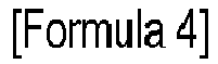

- 21. The organic light emitting display device according to clause 18, wherein the fluorescent compound in the first blue emitting material layer is represented by Formula 9:


- 22. The organic light emitting display device according to clause 21, wherein the fluorescent compound in the first blue emitting material layer is one of compounds in Formula 10:
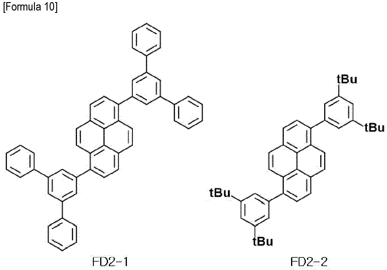

- 23. The organic light emitting display device according to clause 15, wherein in the second organic light emitting diode, the organic light emitting layer includes a first emitting part including a first red emitting material layer and a second emitting part including a second red emitting material layer and positioned between the first emitting part and the transparent electrode,
- wherein the first red emitting material layer is a florescent emitting layer, and the second red emitting material layer is a phosphorescent emitting layer,
- wherein in the third organic light emitting diode, the organic light emitting layer includes a first emitting part including a first green emitting material layer and a second emitting part including a second green emitting material layer and positioned between the first emitting part and the transparent electrode,
- wherein the first green emitting material layer is a phosphorescent emitting layer, and the second green emitting material layer is a florescent emitting layer.
- 24. The organic light emitting display device according to clause 23, wherein the second red emitting material layer has an emitting efficiency being greater than the first red emitting material layer, and the second green emitting material layer has an emitting efficiency being greater than the first green emitting material layer.
- 25. The organic light emitting display device according to clause 15, wherein the organic light emitting layer in the first organic light emitting diode further includes a third emitting material layer and positioned between the first and second emitting parts, wherein the third emitting material layer emits red light and green light, and
wherein each of the second and third organic light emitting diodes has the same structure as the first organic light emitting diode. - 26. The organic light emitting display device according to clause 25, further comprising: a color filter layer positioned between the substrate and each of the first to third organic light emitting diodes or over each of the first to third organic light emitting diodes.
- 27. The organic light emitting display device according to clause 15, wherein each of the second and third organic light emitting diodes has the same structure as the first organic light emitting diode, and
wherein the organic light emitting display device further comprises: a color conversion layer positioned between the substrate and each of the first and second organic light emitting diodes or over each of the first and second organic light emitting diodes.
Claims (15)
- An organic light emitting diode, comprising:a reflective electrode;a transparent electrode facing the reflective electrode; anda first emitting part including a first blue emitting material layer and positioned between the reflective electrode and the transparent electrode, the first blue emitting material layer including a fluorescent compound;a second emitting part including a second blue emitting material layer and positioned between the first emitting part and the transparent electrode, the second blue emitting material layer including a fluorescent compound and a phosphorescent compound; anda charge generation layer positioned between the first and second emitting parts;wherein a difference between a second emission peak intensity of the fluorescent compound in the second blue emitting material layer and a second emission peak intensity of the fluorescent compound in the first blue emitting material layer is 0.1 or less.
- The organic light emitting diode according to claim 1, wherein a difference between a maximum emission wavelength of the fluorescent compound in the first blue emitting material layer and a maximum emission wavelength of the fluorescent compound in the second blue emitting material layer is 15nm or less.
- The organic light emitting diode according to claim 1 or 2, wherein in the second blue emitting material layer, a difference between a maximum absorption wavelength of the fluorescent compound and a maximum emission wavelength of the phosphorescent compound is 10nm or less.
- The organic light emitting diode according to any preceding claim, wherein in the second blue emitting material layer, the fluorescent compound is represented by Formula 1:
 wherein each of R1 and R2 is independently selected from the group consisting of deuterium, a substituted or unsubstituted C5 to C30 heteroaryl group and a substituted or unsubstituted C6 to C30 arylamine group,wherein each of R3, R4, R5 and R6 is independently selected from the group consisting of deuterium, a substituted or unsubstituted C1 to C10 alkyl group and a substituted or unsubstituted C6 to C30 aryl group,wherein each of n1 and n2 is independently an integer of 0 to 3, and each of n3, n4, n5 and n6 is independently an integer of 0 to 5, and/orwherein the phosphorescent compound is represented by Formula 3:
 wherein each of R21, R22 and R23 is independently selected from the group consisting of a substituted or unsubstituted C1 to C10 alkyl group, a substituted or unsubstituted C6 to C30 aryl group and a substituted or unsubstituted C5 to 30 heteroaryl group,wherein b1 is an integer of 0 to 2, b2 is an integer of 0 to 4, and b3 is an integer of 0 to 3,wherein R24 is selected from the group consisting of absent, hydrogen, a substituted or unsubstituted C1 to C10 alkyl group, a substituted or unsubstituted C6 to C30 aryl group and a substituted or unsubstituted C5 to 30 heteroaryl group.
 - The organic light emitting diode according to claim 4, wherein the fluorescent compound in the second blue emitting material layer is one of compounds in Formula 2:

- The organic light emitting diode according to claim 4 or 5, wherein the phosphorescent compound in the second blue emitting material layer is one of compounds in Formula 4:

- The organic light emitting diode according to any preceding claim, wherein the second blue emitting material layer further includes a first host and a second host,wherein the first host is represented by Formula 5:

 wherein each of R31, R32, R33, R34, R35 and R36 is independently selected from the group consisting of a substituted or unsubstituted C1 to C10 alkyl group, a substituted or unsubstituted C6 to C30 aryl group and a substituted or unsubstituted C5 to C30 heteroaryl group,wherein each of c1, c2, c3, c4, c5 and c6 is independently an integer of 0 to 4,wherein the first host is represented by Formula 7:
 wherein each of R41, R42, R43 and R44 is independently selected from the group consisting of a substituted or unsubstituted C1 to C10 alkyl group, a substituted or unsubstituted C6 to C30 aryl group and a substituted or unsubstituted C5 to 30 heteroaryl group, andwherein each of d1, d2, d3 and d4 is independently an integer of 0 to 4, optionally wherein the first host is one of compounds in Formula 6:

 wherein the second host is one of compounds in Formula 8:

- The organic light emitting diode according to any preceding claim, wherein the fluorescent compound in the first blue emitting material layer is represented by Formula 9:


- The organic light emitting diode according to claim 8, wherein the fluorescent compound in the first blue emitting material layer is one of compounds in Formula 10:


- The organic light emitting diode according to any preceding claim, wherein the first blue emitting material layer further includes a host represented by Formula 11:
 wherein each of R51, R52, R53, R54, R55 and R56 is independently selected from the group consisting of a substituted or unsubstituted C1 to C10 alkyl group, a substituted or unsubstituted C6 to C30 aryl group and a substituted or unsubstituted C5 to C30 heteroaryl group, andwherein each of e1, e2, e3, e4, e5 and e6 is independently an integer of 0 to 4, optionally wherein the host in the first blue emitting material layer is one of compounds in Formula 12:
- The organic light emitting diode according to any preceding claim, further comprising: a third emitting part including a third emitting material layer and positioned between the first and second emitting parts, wherein the third emitting material layer emits red light and yellow-green light.
- An organic light emitting display device, comprising:a substrate including a blue pixel region, a red pixel region and a green pixel region; andfirst to third organic light emitting diodes positioned over the substrate and respectively corresponding to the blue pixel region, the red pixel region and the green pixel region, each of the first to third organic light emitting diodes including:a reflective electrode;a transparent electrode facing the reflective electrode; andan organic light emitting layer between the reflective electrode and the transparent electrode,wherein in the first organic light emitting diode, the organic light emitting layer includes a first emitting part including a first blue emitting material layer a second emitting part including a second blue emitting material layer and positioned between the first emitting part and the transparent electrode;a charge generation layer positioned between the first and second emitting parts;wherein the first blue emitting material layer includes a fluorescent compound, and the second blue emitting material layer includes a fluorescent compound and a phosphorescent compound, andwherein a difference between a second emission peak intensity of the fluorescent compound in the second blue emitting material layer and a second emission peak intensity of the fluorescent compound in the first blue emitting material layer is 0.1 or less.
- The organic light emitting display device according to claim 12, wherein the first organic light emitting diode is an organic light emitting diode according to any one of claims 1-11.
- The organic light emitting display device according to claim 12 or 13, wherein in the second organic light emitting diode, the organic light emitting layer includes a first emitting part including a first red emitting material layer and a second emitting part including a second red emitting material layer and positioned between the first emitting part and the transparent electrode,wherein the first red emitting material layer is a florescent emitting layer, and the second red emitting material layer is a phosphorescent emitting layer,wherein in the third organic light emitting diode, the organic light emitting layer includes a first emitting part including a first green emitting material layer and a second emitting part including a second green emitting material layer and positioned between the first emitting part and the transparent electrode,wherein the first green emitting material layer is a phosphorescent emitting layer, and the second green emitting material layer is a florescent emitting layer, optionally, wherein the second red emitting material layer has an emitting efficiency being greater than the first red emitting material layer, and the second green emitting material layer has an emitting efficiency being greater than the first green emitting material layer.
- The organic light emitting display device according to any of claims 12-14, wherein each of the second and third organic light emitting diodes has the same structure as the first organic light emitting diode, optionallywherein the organic light emitting display device, further comprises: a color filter layer positioned between the substrate and each of the first to third organic light emitting diodes or over each of the first to third organic light emitting diodes; orwherein the organic light emitting display device further comprises: a color conversion layer positioned between the substrate and each of the first and second organic light emitting diodes or over each of the first and second organic light emitting diodes.
Applications Claiming Priority (1)
| Application Number | Priority Date | Filing Date | Title |
|---|---|---|---|
| KR1020210189586A KR102956288B1 (en) | 2021-12-28 | 2021-12-28 | Organic light emitting diode and organic light emitting display device including the same |
Publications (2)
| Publication Number | Publication Date |
|---|---|
| EP4207967A2 true EP4207967A2 (en) | 2023-07-05 |
| EP4207967A3 EP4207967A3 (en) | 2023-09-06 |
Family
ID=83995080
Family Applications (1)
| Application Number | Title | Priority Date | Filing Date |
|---|---|---|---|
| EP22203390.4A Pending EP4207967A3 (en) | 2021-12-28 | 2022-10-24 | Organic light emitting diode and organic light emitting display device including the same |
Country Status (4)
| Country | Link |
|---|---|
| US (1) | US20230210001A1 (en) |
| EP (1) | EP4207967A3 (en) |
| KR (1) | KR102956288B1 (en) |
| CN (1) | CN116367570A (en) |
Family Cites Families (5)
| Publication number | Priority date | Publication date | Assignee | Title |
|---|---|---|---|---|
| EP1437395B2 (en) * | 2002-12-24 | 2015-08-26 | LG Display Co., Ltd. | Organic electroluminescent device |
| JP6151873B1 (en) | 2017-02-10 | 2017-06-21 | Lumiotec株式会社 | Organic electroluminescent device, display device, lighting device |
| CN116987108A (en) * | 2017-05-16 | 2023-11-03 | 学校法人关西学院 | Polycyclic aromatic compound, material for organic element, composition for forming light-emitting layer, organic electroluminescent element, and device |
| US11690285B2 (en) | 2018-11-28 | 2023-06-27 | Universal Display Corporation | Electroluminescent devices |
| KR102731161B1 (en) * | 2019-12-31 | 2024-11-15 | 엘지디스플레이 주식회사 | Organic Light Emitting Element and Display Device Using the Same |
-
2021
- 2021-12-28 KR KR1020210189586A patent/KR102956288B1/en active Active
-
2022
- 2022-10-24 EP EP22203390.4A patent/EP4207967A3/en active Pending
- 2022-12-02 US US18/074,194 patent/US20230210001A1/en active Pending
- 2022-12-28 CN CN202211699210.5A patent/CN116367570A/en active Pending
Also Published As
| Publication number | Publication date |
|---|---|
| EP4207967A3 (en) | 2023-09-06 |
| CN116367570A (en) | 2023-06-30 |
| KR102956288B1 (en) | 2026-04-22 |
| US20230210001A1 (en) | 2023-06-29 |
| KR20230100043A (en) | 2023-07-05 |
Similar Documents
| Publication | Publication Date | Title |
|---|---|---|
| KR102727943B1 (en) | Organic light emitting diode and organic light emitting device having thereof | |
| KR102839063B1 (en) | Organic light emitting diode and organic light emitting device having thereof | |
| KR102733723B1 (en) | Organic light emitting diode and organic light emitting device having thereof | |
| KR102733724B1 (en) | Organic light emitting diode and organic light emitting device having thereof | |
| CN112864332A (en) | Organic light emitting diode and organic light emitting device including the same | |
| US20230189628A1 (en) | Organic light emitting diode and organic light emitting display device including the same | |
| US20240244857A1 (en) | Organic compound, organic light emitting diode and organic light emitting device having the compound | |
| US12575322B2 (en) | Organic light emitting diode and organic light emitting display device including the same | |
| KR102927534B1 (en) | Organic light emitting diode and organic light emitting display device including the same | |
| CN117956817A (en) | Organic light emitting diode and organic light emitting device including the same | |
| CN117956816A (en) | Organic light emitting diode and organic light emitting device including the same | |
| EP4203645A2 (en) | Organic light emitting diode and organic light emitting display device including the same | |
| US20230210001A1 (en) | Organic light emitting diode and organic light emitting display device including the same | |
| US20220149296A1 (en) | Organic light emitting diode and organic light emitting device including the same | |
| US20240244967A1 (en) | Organic Light Emitting Diode and Organic Light Emitting Device Including the Same | |
| US20240237377A1 (en) | Organic light emitting diode and organic light emitting display device including the same | |
| EP4195903A1 (en) | Organic light emitting display device | |
| CN115835670B (en) | Organic light-emitting diode and organic light-emitting device having the organic light-emitting diode | |
| US20250241118A1 (en) | Organic light emitting diode and organic light emitting device including the same | |
| EP4199686A1 (en) | Organic light emitting diode and organic light emitting device including the same | |
| US20240237525A1 (en) | Organic Light Emitting Diode and Organic Light Emitting Device Including the Same | |
| US20230200231A1 (en) | Organic light emitting diode and organic light emitting display device including the same | |
| US20240179932A1 (en) | Organic light emitting diode and organic light emitting device including the same | |
| CN118265327A (en) | Organic light emitting diode and organic light emitting device including the same | |
| CN120548020A (en) | Organic light emitting diode and organic light emitting device including the same |
Legal Events
| Date | Code | Title | Description |
|---|---|---|---|
| PUAI | Public reference made under article 153(3) epc to a published international application that has entered the european phase |
Free format text: ORIGINAL CODE: 0009012 |
|
| STAA | Information on the status of an ep patent application or granted ep patent |
Free format text: STATUS: REQUEST FOR EXAMINATION WAS MADE |
|
| 17P | Request for examination filed |
Effective date: 20221024 |
|
| AK | Designated contracting states |
Kind code of ref document: A2 Designated state(s): AL AT BE BG CH CY CZ DE DK EE ES FI FR GB GR HR HU IE IS IT LI LT LU LV MC ME MK MT NL NO PL PT RO RS SE SI SK SM TR |
|
| PUAL | Search report despatched |
Free format text: ORIGINAL CODE: 0009013 |
|
| AK | Designated contracting states |
Kind code of ref document: A3 Designated state(s): AL AT BE BG CH CY CZ DE DK EE ES FI FR GB GR HR HU IE IS IT LI LT LU LV MC ME MK MT NL NO PL PT RO RS SE SI SK SM TR |
|
| RIC1 | Information provided on ipc code assigned before grant |
Ipc: H10K 101/10 20230101ALN20230728BHEP Ipc: H10K 85/60 20230101ALN20230728BHEP Ipc: H10K 85/30 20230101ALN20230728BHEP Ipc: H10K 50/19 20230101ALI20230728BHEP Ipc: H10K 50/11 20230101AFI20230728BHEP |
|
| RBV | Designated contracting states (corrected) |
Designated state(s): AL AT BE BG CH CY CZ DE DK EE ES FI FR GB GR HR HU IE IS IT LI LT LU LV MC ME MK MT NL NO PL PT RO RS SE SI SK SM TR |
|
| STAA | Information on the status of an ep patent application or granted ep patent |
Free format text: STATUS: EXAMINATION IS IN PROGRESS |
|
| 17Q | First examination report despatched |
Effective date: 20250113 |