EP4207613A1 - Isolated driver device and method of transmitting information in an isolated driver device - Google Patents
Isolated driver device and method of transmitting information in an isolated driver device Download PDFInfo
- Publication number
- EP4207613A1 EP4207613A1 EP22211470.4A EP22211470A EP4207613A1 EP 4207613 A1 EP4207613 A1 EP 4207613A1 EP 22211470 A EP22211470 A EP 22211470A EP 4207613 A1 EP4207613 A1 EP 4207613A1
- Authority
- EP
- European Patent Office
- Prior art keywords
- signal
- semiconductor die
- circuit
- modulation
- fault
- Prior art date
- Legal status (The legal status is an assumption and is not a legal conclusion. Google has not performed a legal analysis and makes no representation as to the accuracy of the status listed.)
- Granted
Links
Images


Classifications
-
- H—ELECTRICITY
- H04—ELECTRIC COMMUNICATION TECHNIQUE
- H04L—TRANSMISSION OF DIGITAL INFORMATION, e.g. TELEGRAPHIC COMMUNICATION
- H04L27/00—Modulated-carrier systems
- H04L27/18—Phase-modulated carrier systems, i.e. using phase-shift keying
- H04L27/20—Modulator circuits; Transmitter circuits
-
- H—ELECTRICITY
- H04—ELECTRIC COMMUNICATION TECHNIQUE
- H04B—TRANSMISSION
- H04B3/00—Line transmission systems
-
- H—ELECTRICITY
- H02—GENERATION; CONVERSION OR DISTRIBUTION OF ELECTRIC POWER
- H02M—APPARATUS FOR CONVERSION BETWEEN AC AND AC, BETWEEN AC AND DC, OR BETWEEN DC AND DC, AND FOR USE WITH MAINS OR SIMILAR POWER SUPPLY SYSTEMS; CONVERSION OF DC OR AC INPUT POWER INTO SURGE OUTPUT POWER; CONTROL OR REGULATION THEREOF
- H02M1/00—Details of apparatus for conversion
- H02M1/0003—Details of control, feedback or regulation circuits
- H02M1/0006—Arrangements for supplying an adequate voltage to the control circuit of converters
-
- H—ELECTRICITY
- H02—GENERATION; CONVERSION OR DISTRIBUTION OF ELECTRIC POWER
- H02M—APPARATUS FOR CONVERSION BETWEEN AC AND AC, BETWEEN AC AND DC, OR BETWEEN DC AND DC, AND FOR USE WITH MAINS OR SIMILAR POWER SUPPLY SYSTEMS; CONVERSION OF DC OR AC INPUT POWER INTO SURGE OUTPUT POWER; CONTROL OR REGULATION THEREOF
- H02M1/00—Details of apparatus for conversion
- H02M1/08—Circuits specially adapted for the generation of control voltages for semiconductor devices incorporated in static converters
-
- H—ELECTRICITY
- H03—ELECTRONIC CIRCUITRY
- H03K—PULSE TECHNIQUE
- H03K19/00—Logic circuits, i.e. having at least two inputs acting on one output; Inverting circuits
- H03K19/20—Logic circuits, i.e. having at least two inputs acting on one output; Inverting circuits characterised by logic function, e.g. AND, OR, NOR, NOT circuits
-
- H—ELECTRICITY
- H04—ELECTRIC COMMUNICATION TECHNIQUE
- H04B—TRANSMISSION
- H04B1/00—Details of transmission systems, not covered by a single one of groups H04B3/00 - H04B13/00; Details of transmission systems not characterised by the medium used for transmission
- H04B1/02—Transmitters
- H04B1/04—Circuits
- H04B1/0466—Fault detection or indication
-
- H—ELECTRICITY
- H04—ELECTRIC COMMUNICATION TECHNIQUE
- H04B—TRANSMISSION
- H04B1/00—Details of transmission systems, not covered by a single one of groups H04B3/00 - H04B13/00; Details of transmission systems not characterised by the medium used for transmission
- H04B1/06—Receivers
- H04B1/16—Circuits
-
- H—ELECTRICITY
- H04—ELECTRIC COMMUNICATION TECHNIQUE
- H04L—TRANSMISSION OF DIGITAL INFORMATION, e.g. TELEGRAPHIC COMMUNICATION
- H04L25/00—Baseband systems
- H04L25/38—Synchronous or start-stop systems, e.g. for Baudot code
- H04L25/40—Transmitting circuits; Receiving circuits
- H04L25/49—Transmitting circuits; Receiving circuits using code conversion at the transmitter; using predistortion; using insertion of idle bits for obtaining a desired frequency spectrum; using three or more amplitude levels ; Baseband coding techniques specific to data transmission systems
- H04L25/4902—Pulse width modulation; Pulse position modulation
-
- H—ELECTRICITY
- H02—GENERATION; CONVERSION OR DISTRIBUTION OF ELECTRIC POWER
- H02M—APPARATUS FOR CONVERSION BETWEEN AC AND AC, BETWEEN AC AND DC, OR BETWEEN DC AND DC, AND FOR USE WITH MAINS OR SIMILAR POWER SUPPLY SYSTEMS; CONVERSION OF DC OR AC INPUT POWER INTO SURGE OUTPUT POWER; CONTROL OR REGULATION THEREOF
- H02M3/00—Conversion of DC power input into DC power output
- H02M3/22—Conversion of DC power input into DC power output with intermediate conversion into AC
- H02M3/24—Conversion of DC power input into DC power output with intermediate conversion into AC by static converters
- H02M3/28—Conversion of DC power input into DC power output with intermediate conversion into AC by static converters using discharge tubes with control electrode or semiconductor devices with control electrode to produce the intermediate AC
- H02M3/325—Conversion of DC power input into DC power output with intermediate conversion into AC by static converters using discharge tubes with control electrode or semiconductor devices with control electrode to produce the intermediate AC using devices of a triode or a transistor type requiring continuous application of a control signal
- H02M3/335—Conversion of DC power input into DC power output with intermediate conversion into AC by static converters using discharge tubes with control electrode or semiconductor devices with control electrode to produce the intermediate AC using devices of a triode or a transistor type requiring continuous application of a control signal using semiconductor devices only
- H02M3/33507—Conversion of DC power input into DC power output with intermediate conversion into AC by static converters using discharge tubes with control electrode or semiconductor devices with control electrode to produce the intermediate AC using devices of a triode or a transistor type requiring continuous application of a control signal using semiconductor devices only with automatic control of the output voltage or current, e.g. flyback converters
Definitions
- the description relates to isolated driver devices and methods of transmitting information (e.g., data) in an isolated driver device.
- Isolated driver devices may be applied, for instance, in traction inverters, DC/DC converters, on-board chargers (OBC), and belt starter generators (BSG) for electric vehicles (EV) and hybrid electric vehicles (HEV).
- OBC on-board chargers
- BSG belt starter generators
- EV electric vehicles
- HEV hybrid electric vehicles
- Conventional isolated gate driver devices comprise two semiconductor dies arranged in the same device package: a low voltage (LV) die that usually exchanges signals with an external control unit (e.g., a microcontroller), and a high voltage (HV) die that includes a driver circuit.
- the low voltage die and the high voltage die are electrically isolated one from the other by a galvanic isolation barrier that usually includes one or more high voltage rating capacitances (HVCap) arranged between the two dies.
- HVCap high voltage rating capacitances
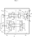
- FIG. 1 is a circuit block diagram exemplary of an isolated gate driver device 10 coupled to a microcontroller 20.
- the driver device 10 comprises a low voltage die 10a and a high voltage die 10b arranged in the same package.
- the driver device 10 comprises a control channel CH PWM (e.g., unidirectional) for transmitting a gate driving pulse-width modulated (PWM) signal from the low voltage die 10a to the high voltage die 10b, and a communication channel CH DATA (e.g., bidirectional) for exchanging an information signal (e.g., data signal) between the low voltage die 10a and the high voltage die 10b.
- CH PWM e.g., unidirectional
- CH DATA e.g., bidirectional
- the control channel CH PWM comprises an input pin 101 configured to receive a pulse-width modulated input signal PWM IN (e.g., single-ended) from the microcontroller 20.
- the frequency of the input signal PWM IN may be, for instance, in the range of 15 kHz to 5 MHz.
- the low voltage portion of the control channel CH PWM comprises a transmitter circuit 102 coupled to the input pin 101 and configured to convert the received PWM signal PWM IN into a pair of differential pulse-width modulated signals OUT P , OUT N .
- signal OUT P may be produced by a non-inverting buffer circuit that receives the input signal PWM IN at input
- signal OUT N may be produced by an inverting buffer circuit that receives the input signal PWM IN at input
- the low voltage portion of the control channel CH PWM further comprises a first high voltage rating capacitance 103P (e.g., an isolation capacitor) having a first terminal coupled to a first output of the transmitter circuit 102 to receive signal OUT P
- a second high voltage rating capacitance 103N e.g., an isolation capacitor
- the second terminals of the capacitances 103P and 103N provide the output nodes of the low voltage portion of the control channel CH PWM , which are connected (e.g., via bonding wires) to the input nodes of the high voltage portion of the control channel CH PWM in the high voltage die 10b.
- the signals OUT P , OUT N are filtered by the isolation capacitors 103P, 103N so that a pulsed differential signal V d reaches the high voltage portion of the control channel CH PWM .
- the differential signal V d comprises a train of pulses (positive and negative) corresponding to the edges (rising and falling, respectively) of the input PWM signal PWM IN .
- the high voltage portion of the control channel CH PWM comprises a receiver circuit 104 coupled to the input nodes of the die 10b to receive the differential signal V d , and configured to produce a reconstructed pulse-width modulated signal PWM RX as a function of the received differential signal V d .
- the receiver circuit 104 may be configured to set the signal PWM RX to a high logic value ('1') as a result of a positive pulse being detected in the differential signal V d , and to a low logic value ('0') as a result of a negative pulse being detected in the differential signal V d . Therefore, the reconstructed signal PWM RX may substantially correspond to a (slightly) delayed copy of the transmitted signal PWM IN .
- the high voltage portion of the control channel CH PWM comprises a driver stage 105 including a pre-driver circuit (e.g., buffers 1051 and 1052) configured to receive the reconstructed signal PWM RX and drive an output switching circuit as a function thereof.
- the output switching circuit may comprise a half-bridge driver stage comprising a high-side transistor and a low-side transistor arranged in series between a high voltage supply pin VH and a high voltage reference pin VL (e.g., ground) of the driver device 10.
- VH high voltage supply pin
- VL high voltage reference pin
- the output switching signal OUT may be used, for instance, to control one or more insulated-gate bipolar transistors (IGBT), silicon carbide transistors (SiC MOSFET) and/or silicon transistors (Si MOSFET) in high-voltage motor control applications.
- IGBT insulated-gate bipolar transistors
- SiC MOSFET silicon carbide transistors
- Si MOSFET silicon transistors
- the communication channel CH DATA comprises a bidirectional communication line 107 (e.g., a communication bus) configured to exchange one or more signals between the microcontroller 20 and the low voltage die 10a.
- the low voltage portion of the communication channel CH DATA comprises a low voltage logic circuit 108 coupled to the communication bus 107 to receive, transmit and process signals from/to the microcontroller 20.
- the logic circuit 108 is coupled to a differential transmitter circuit 109 configured to transmit an information signal (e.g., data signal) towards the high voltage portion of the communication channel CH DATA , and a differential receiver circuit 110 configured to receive an information signal (e.g., data signal) from the high voltage portion of the communication channel CH DATA .
- the differential output of the transmitter circuit 109 and the differential input of the receiver circuit 110 are coupled to the first terminals of a pair of high voltage rating capacitances 111P and 111N (e.g., isolation capacitors).
- the second terminals of the capacitances 111P and 111N provide the input/output nodes of the low voltage portion of the communication channel CH DATA , which are connected (e.g., via bonding wires) to the input/output nodes of the high voltage portion of the communication channel CH DATA in the high voltage die 10b.
- the high voltage portion of the communication channel CH DATA comprises a differential receiver circuit 112 coupled to the input/output nodes of the die 10b and configured to receive the information signal from the low voltage portion of the communication channel CH DATA , and a differential transmitter circuit 113 coupled to the input/output nodes of the die 10b and configured to transmit an information signal towards the low voltage portion of the communication channel CH DATA .
- the high voltage portion of the communication channel CH DATA comprises a high voltage logic circuit 114 coupled to the differential receiver circuit 112 and the differential transmitter circuit 113 to receive, transmit and process the information signal.
- a complete integrated bidirectional communication channel CH DATA includes a transmission-receiver (TX-RX) differential interface and an isolation barrier (e.g., a pair of isolation capacitors 111P and 111N) between the two dies 10a and 10b.
- TX-RX transmission-receiver
- isolation barrier e.g., a pair of isolation capacitors 111P and 111N
- a control channel CH PWM can be mainly employed for transmitting a PWM gate control signal between the different voltage sections of the isolated driver device 10.
- a data communication channel CH DATA can be mainly employed for transmitting an information signal between the different voltage sections of the isolated driver device 10.
- a plurality of communication channels (not visible in Figure 1 ) can be provided in an isolated driver device to implement additional functions.
- a bidirectional communication protocol which allows for data exchange between the two dies, can be used for overall device configuration, register readout and fault management. One of the information carried may thus regard the detection of faults.
- a failure event e.g., a fault
- the system has to wait for the end of an ongoing HV to LV data transmission and the subsequent LV to HV reverse data flow, before being able to use the communication channel CH DATA to communicate the detected fault to the external control unit 20.
- reacting rapidly on faults represents a desirable feature and a communication delay as described above may be undesirable.
- Driver devices known in the art may provide a faster path for critical fault detection resorting to the use of an additional (e.g., autonomous or dedicated) HV-to-LV communication channel so as to bypass the bidirectional data flow interface protocol of a standard communication channel CH DATA .
- an additional high voltage rating capacitance e.g., an additional isolation capacitor
- TX-RX circuitry which result in larger silicon area occupation.
- An object of one or more embodiments is to contribute in providing such improved isolated driver devices.
- such an object can be achieved by an electronic device having the features set forth in the claims that follow.
- One or more embodiments may relate to a corresponding method of transmitting information in an electronic device.
- an electronic device comprises a first semiconductor die (e.g., low voltage die) and a second semiconductor die (e.g., high voltage die) galvanically isolated from each other.
- the second semiconductor die includes a signal modulator circuit configured to modulate a carrier signal to produce a modulated signal encoding information.
- a galvanically isolated communication channel implemented in the first semiconductor die and the second semiconductor die is configured to transmit the modulated signal from the second semiconductor die to the first semiconductor die.
- the second semiconductor die includes a fault detection circuit configured to detect electrical faults in the second semiconductor die.
- the second semiconductor die further includes a logic circuit coupled to the fault detection circuit and configured to assert a modulation bypass signal in response to a fault being detected by the fault detection circuit.
- the second semiconductor die further includes modulation masking circuitry configured to force the modulated signal to a steady value over a plurality of periods of the carrier signal in response to the modulation bypass signal being asserted.
- the first semiconductor die includes a respective logic circuit sensitive to the modulated signal and configured to detect a condition where the modulated signal has a steady value over a plurality of periods of the carrier signal, and to assert a fault detection signal in response to the condition being detected.
- One or more embodiments thus facilitate fast detection of faults in the second semiconductor die without resorting to a dedicated fault detection communication channel between the two semiconductor dies.
- the modulation bypass signal may be asserted-high
- the modulation masking circuitry may comprise an inverter circuit configured to produce the complement signal of the modulation bypass signal, and an AND logic gate configured to combine the complement signal of the modulation bypass signal and the modulated signal to force the modulated signal to a low logic value.
- the modulation bypass signal may be asserted-low
- the modulation masking circuitry may comprise an AND logic gate configured to combine the modulation bypass signal and the modulated signal to force the modulated signal to a low logic value.
- the modulation bypass signal may be asserted-low
- the modulation masking circuitry may comprise an inverter circuit configured to produce the complement signal of the modulation bypass signal, and an OR logic gate configured to combine the complement signal of the modulation bypass signal and the modulated signal to force the modulated signal to a high logic value.
- the modulation bypass signal may be asserted-high
- the modulation masking circuitry may comprise an OR logic gate configured to combine the modulation bypass signal and the modulated signal to force the modulated signal to a high logic value.
- the galvanically isolated communication channel may include a transmitter circuit implemented in the second semiconductor die, at least one isolation capacitor and a receiver circuit implemented in the first semiconductor die, and electrically conductive means coupling the transmitter circuit to the at least one isolation capacitor.
- the first semiconductor die may include a respective fault detection circuit configured to detect electrical faults in the first semiconductor die, and the respective logic circuit may be further configured to assert the fault detection signal in response to a fault being detected by the respective fault detection circuit.
- the carrier signal may be modulated according to a pulse-width modulation to produce the modulated signal encoding information.
- the modulation masking circuitry may be configured to force the modulated signal to a steady value for a duration of ten or less periods of the carrier signal, optionally five or less periods of the carrier signal, optionally four periods of the carrier signal, three periods of the carrier signal, or two periods of the carrier signal.
- the modulation masking circuitry may be configured to force the modulated signal to a steady value until the fault detection signal is asserted by the respective logic circuit.
- the electronic device may further comprise an input node configured to receive a pulse-width modulated control signal, and a second galvanically isolated communication channel implemented in the first semiconductor die and the second semiconductor die and configured to transmit the pulse-width modulated control signal from the first semiconductor die to the second semiconductor die.
- the second semiconductor die may include a driver circuit configured to receive the pulse-width modulated control signal and produce an output switching signal.
- the driver circuit may include a half-bridge circuit arranged between a positive supply voltage pin and a reference supply voltage pin.
- the modulated signal may encode a value of a supply voltage at the positive supply voltage pin.
- an electronic system may comprise a processing unit configured to generate a pulse-width modulated control signal, an electronic device according to one or more embodiments coupled to the processing unit to receive therefrom the pulse-width modulated control signal and to transmit thereto the fault detection signal, and a voltage regulator circuit configured to produce the supply voltage at the positive supply voltage pin.
- an electronic system may further comprise a capacitor coupled to the positive supply voltage pin.
- a method of transmitting information in an electronic device may comprise:
- references to "an embodiment” or “one embodiment” in the framework of the present description is intended to indicate that a particular configuration, structure, or characteristic described in relation to the embodiment is comprised in at least one embodiment.
- phrases such as “in an embodiment” or “in one embodiment” that may be present in one or more points of the present description do not necessarily refer to one and the same embodiment.
- particular configurations, structures, or characteristics may be combined in any adequate way in one or more embodiments.
- Figure 2 is a circuit block diagram exemplary of communication channels in an isolated driver device.
- Figure 2 shows certain components of a conventional isolated driver device provided with a dedicated HV-to-LV unidirectional communication channel for fast detection of faults in the high voltage die 10b.
- the low voltage die 10a comprises a low voltage digital circuit 108' (e.g., including the low voltage logic circuit 108) coupled to a bidirectional communication channel CH DATA .
- the high voltage die 10b comprises a high voltage digital circuit 114' (e.g., including the high voltage logic circuit 114) coupled to the bidirectional communication channel CH DATA .
- the bidirectional communication channel CH DATA includes a transmitter circuit 109, a receiver circuit 110, isolation capacitors 111P and 111N, a receiver circuit 112 and a transmitter circuit 113 as described with reference to Figure 1 . It is noted that the transmitter and receiver circuits 109, 110, 112 and 113 are illustrated as single-ended circuits for the sake of ease of illustration only, but they may include differential circuits as described with reference to Figure 1 .
- the driver device comprises a dedicated HV-to-LV unidirectional communication channel CH FAULT from the high voltage die 10b to the low voltage die 10a, the channel CH FAULT including a respective transmitter circuit 115 in the high voltage die 10b, and respective isolation capacitor(s) 116 and receiver circuit 117 in the low voltage die 10a.
- the transmitter circuit 115, the receiver circuit 117 and the isolation capacitor(s) 116 are illustrated as single-ended circuits for the sake of ease of illustration only, but they may include differential circuits as described with reference to Figure 1 .
- the high voltage digital circuit 114' may comprise a high voltage diagnosis circuit 118 configured to produce a fault signal indicative of a fault being detected in the high voltage die 10b (e.g., the fault signal being asserted in response to a detected fault).
- the fault signal may be transmitted via the bidirectional channel CH DATA and/or the unidirectional dedicated channel CH FAULT .
- the low voltage digital circuit 108' may comprise a low voltage diagnosis circuit 119 configured to produce a respective fault signal indicative of a fault being detected in the low voltage die 10a (e.g., the respective fault signal being asserted in response to a detected fault).
- a first output 120a of the low voltage digital circuit 108' may provide a serial data output (SDO) signal produced by a serial peripheral interface (SPI) 121 as a function of the data signal received from the communication channel CH DATA and the diagnosis signal produced by the diagnosis circuit 119, e.g., as an OR combination (OR logic gate) of the data signal and diagnosis signal.
- a second output 120b of the low voltage digital circuit 108' may provide a slow fault detection signal produced as a function of the data signal received from the communication channel CH DATA and the diagnosis signal produced by the diagnosis circuit 119, e.g., as a NOR combination (NOR logic gate) of the data signal and diagnosis signal.
- a third output 120c of the low voltage digital circuit 108' may provide a fast fault detection signal produced as a function of the data signal received from the unidirectional channel CH FAULT and the diagnosis signal produced by the diagnosis circuit 119, e.g., as a NOR combination (NOR logic gate) of the two signals.
- faults detected in the high voltage die 10b can be communicated to an external control unit via a slower communication path resorting to a bidirectional communication channel CH DATA , and/or via a faster communication path resorting to a dedicated unidirectional communication channel CH AULT .
- the fault detection time may be as short as the TX-RX chain propagation delay.
- implementing a faster path CH FAULT for critical fault detection involves the use of a dedicated HV-to-LV channel in order to bypass the bidirectional interface data flow of channel CH DATA , resulting in large silicon area occupation due to the integration of large high voltage capacitor(s) 116 (e.g., having a voltage rating in the order of some kV) and related TX-RX circuitry 115 and 117.
- large high voltage capacitor(s) 116 e.g., having a voltage rating in the order of some kV
- one or more embodiments may rely on the presence of other communication channel(s) that are often integrated for device-specific functions, other than communication and driver control.
- an isolated driver device 10 may comprise a communication channel CH' DATA configured to transmit a modulated signal (e.g., a feedback signal, possibly modulated according to a PWM modulation) following the HV to LV data flow, i.e., from the high voltage die 10b to the low voltage die 10a.
- a modulated signal e.g., a feedback signal, possibly modulated according to a PWM modulation
- a logical conditioning may be applied to the modulated signal to temporarily "mask" the modulated signal transmitted via the channel CH' DATA .
- the low voltage logic circuit 108 may be configured to sense the "masking" (e.g., loss of information) of the modulated signal, and consequently assert a (fast) fault signal FAULT at an output 120d of the low voltage die 10a.
- such an approach to fast fault detection may be advantageous insofar as the temporary masking of the modulated signal (e.g., lack of information in the modulated signal) transmitted via the channel CH' DATA does not affect the operation of the device (e.g., does not affect other device specifications).
- a transparent reaction to fast masking transient of the channel CH' DATA can be modeled (e.g., implemented) as a low-pass filtering in the signal flow path.
- an isolated driver device 10 may comprise a high voltage die 10b and a low voltage die 10a electrically isolated by an isolation barrier, and a communication channel CH' DATA configured to transmit a modulated signal MOD (e.g., an information signal or a feedback signal) from the high voltage die 10b to the low voltage die 10a.
- the communication channel CH' DATA may be unidirectional (from the high voltage die to the low voltage die) or bidirectional, and may include a (differential) transmitter circuit 113' in the high voltage die 10b, as well as isolation capacitor(s) 111P', 111N' and a (differential) receiver circuit 110' in the low voltage die 10a.
- the high voltage die 10b may comprise a signal modulator circuit 122 configured to produce a modulated signal FB carrying some sort of information (e.g., a feedback, a reading value from a sensor, and the like).
- the high voltage die 10b may further comprise a high voltage diagnosis circuit 118 coupled to a logic circuit 114.
- the diagnosis circuit 118 may be configured to assert a high-voltage fault signal HV FAULT indicative of a fault being detected in the high voltage die 10b, and the logic circuit 114 may be configured to assert a signal BP (e.g., a modulation bypass signal) in response to the high-voltage fault signal HV_FAULT being asserted.
- BP e.g., a modulation bypass signal
- the bypass signal BP may be kept asserted for a certain period of time (e.g., fixed or programmable) t bypass , and may be de-asserted again at the end of the period of time t bypass .
- the high voltage die 10b may comprise logic circuitry 123 configured to mask (e.g., set to a low logic value) the modulated signal FB in response to the bypass signal BP being asserted.
- the masking circuitry 123 may comprise an inverter circuit 124 configured to produce the complement of the bypass signal BP, and an AND gate 125 configured to combine the complement of the bypass signal BP and the modulated signal FB to produce the output modulated signal MOD, where the output modulated signal MOD is "masked" when forced to a low logic value over plural periods.
- the masking circuitry 123 may comprise an OR gate configured to combine the bypass signal BP and the modulated signal FB to produce the output modulated signal MOD, where the output modulated signal MOD is "masked” when forced to a high logic value over plural periods.
- the modulated signal MOD as received at the low voltage die 10a may include a portion (see Figure 4 ) where the information content is masked and the signal is kept to the same logic value (e.g., low) over multiple periods.
- the logic circuit 108 in the low voltage die 10a may be configured to detect such loss of information in the modulated signal MOD_LV, and consequently assert the output fault signal FAULT at node 120d for transmission to the microcontroller 20.
- the value of the modulated signals MOD and MOD_LV may be masked for a short period of time t bypass (e.g., one period, two periods, three periods, etc. up to five or ten periods).
- the value of the modulated signals MOD and MOD_LV may be masked until the fault signal FAULT produced by the logic circuit 108 and monitored by the microcontroller 20 is asserted (e.g., the modulated signal MOD may be de-masked as soon as the microcontroller 20 acknowledges detection of a fault). Overall, a short period of time t detect may be needed to assert the fault signal FAULT after detection of a fault in the high voltage die 10b.
- Figures 5 and 6 are circuit block diagrams exemplary of a possible application of one or more embodiments.
- the isolated driver device 10 exemplified in Figure 5 includes a bidirectional communication channel CH DATA and a unidirectional control channel CH PWM substantially as disclosed with reference to Figure 1 .
- the isolated driver device 10 comprises a further (unidirectional, in the present example) communication channel CH' DATA configured to transmit a feedback signal from the high voltage die 10b to the low voltage die 10a.
- the communication channel CH' DATA is configured to regulate in a closed loop the positive supply rail VH generated by an isolated external flyback network 50 (or any other suitable DC-DC converter) for the high voltage driver stage 105.
- the secondary output of a transformer included in the flyback network 50 may be sensed at the high voltage die 10b and the information about the voltage level of the positive supply rail VH can be encoded by modulating the duty-cycle of a fixed frequency PWM signal at a flyback control circuit 502, thereby producing a modulated feedback signal PWM FLY .
- Fault detection circuitry 118 and masking circuitry 123 can be provided in the high voltage die 10b to act on the feedback signal PWM FLY and temporarily mask its value as a result of a fault being detected.
- the value of the feedback signal PWM FLY may be masked for a short period of time (e.g., one period, two periods, three periods, etc. up to five or ten periods). Additionally or alternatively, the value of the feedback signal PWM FLY may be masked until the fault signal FAULT produced by the logic circuit 108 in the low voltage die 10a and monitored by the microcontroller 20 is asserted.
- FIG. 7 is a further circuit block diagram that shows, in a simplified manner, the provision of fault detection circuitry and masking circuitry in a flyback feedback channel CH' DATA as discussed with reference to Figures 5 and 6 .
- the flyback regulation feature e.g., circuit 502
- the fast fault detection feature e.g., circuits 118, 114, 123 may share the same communication channel CH' DATA .
- the temporary lack of information in the flyback feedback signal does not affect the output battery regulation (i.e., the voltage at rail VH), insofar as a rectification capacitor C F is coupled to the secondary winding of the flyback transformer.
- the channel CH' DATA may be an information channel used mainly for transmitting information from a sensor to the microcontroller 20 via the low voltage die 10a (e.g., a temperature sensor or the like).
- one or more embodiments may rely on the use of a same communication channel CH' DATA for both a dedicated device function (e.g., flyback output regulation) and for HV-fault fast detection, thereby advantageously providing fast fault detection without increasing the silicon area occupation (e.g., because no extra high-voltage capacitor and related TX-RX channel circuitry has to be implemented).
- a dedicated device function e.g., flyback output regulation
- HV-fault fast detection e.g., flyback output regulation
Landscapes
- Engineering & Computer Science (AREA)
- Computer Networks & Wireless Communication (AREA)
- Signal Processing (AREA)
- Physics & Mathematics (AREA)
- Power Engineering (AREA)
- Spectroscopy & Molecular Physics (AREA)
- Computer Hardware Design (AREA)
- Computing Systems (AREA)
- General Engineering & Computer Science (AREA)
- Mathematical Physics (AREA)
- Dc Digital Transmission (AREA)
- Stored Programmes (AREA)
Abstract
Description
- The description relates to isolated driver devices and methods of transmitting information (e.g., data) in an isolated driver device.
- Isolated driver devices (e.g., gate driver devices) may be applied, for instance, in traction inverters, DC/DC converters, on-board chargers (OBC), and belt starter generators (BSG) for electric vehicles (EV) and hybrid electric vehicles (HEV).
- Conventional isolated gate driver devices comprise two semiconductor dies arranged in the same device package: a low voltage (LV) die that usually exchanges signals with an external control unit (e.g., a microcontroller), and a high voltage (HV) die that includes a driver circuit. The low voltage die and the high voltage die are electrically isolated one from the other by a galvanic isolation barrier that usually includes one or more high voltage rating capacitances (HVCap) arranged between the two dies.
-
Figure 1 is a circuit block diagram exemplary of an isolatedgate driver device 10 coupled to amicrocontroller 20. Thedriver device 10 comprises alow voltage die 10a and ahigh voltage die 10b arranged in the same package. Thedriver device 10 comprises a control channel CHPWM (e.g., unidirectional) for transmitting a gate driving pulse-width modulated (PWM) signal from thelow voltage die 10a to thehigh voltage die 10b, and a communication channel CHDATA (e.g., bidirectional) for exchanging an information signal (e.g., data signal) between thelow voltage die 10a and thehigh voltage die 10b. - The control channel CHPWM comprises an
input pin 101 configured to receive a pulse-width modulated input signal PWMIN (e.g., single-ended) from themicrocontroller 20. The frequency of the input signal PWMIN may be, for instance, in the range of 15 kHz to 5 MHz. In thelow voltage die 10a, the low voltage portion of the control channel CHPWM comprises atransmitter circuit 102 coupled to theinput pin 101 and configured to convert the received PWM signal PWMIN into a pair of differential pulse-width modulated signals OUTP, OUTN. For instance, signal OUTP may be produced by a non-inverting buffer circuit that receives the input signal PWMIN at input, and signal OUTN may be produced by an inverting buffer circuit that receives the input signal PWMIN at input. The low voltage portion of the control channel CHPWM further comprises a first highvoltage rating capacitance 103P (e.g., an isolation capacitor) having a first terminal coupled to a first output of thetransmitter circuit 102 to receive signal OUTP, and a second highvoltage rating capacitance 103N (e.g., an isolation capacitor) having a first terminal coupled to a second output of thetransmitter circuit 102 to receive signal OUTN. The second terminals of thecapacitances high voltage die 10b. The signals OUTP, OUTN are filtered by theisolation capacitors - The high voltage portion of the control channel CHPWM comprises a
receiver circuit 104 coupled to the input nodes of thedie 10b to receive the differential signal Vd , and configured to produce a reconstructed pulse-width modulated signal PWMRX as a function of the received differential signal Vd . For instance, thereceiver circuit 104 may be configured to set the signal PWMRX to a high logic value ('1') as a result of a positive pulse being detected in the differential signal Vd, and to a low logic value ('0') as a result of a negative pulse being detected in the differential signal Vd. Therefore, the reconstructed signal PWMRX may substantially correspond to a (slightly) delayed copy of the transmitted signal PWMIN. The high voltage portion of the control channel CHPWM comprises adriver stage 105 including a pre-driver circuit (e.g.,buffers 1051 and 1052) configured to receive the reconstructed signal PWMRX and drive an output switching circuit as a function thereof. For instance, the output switching circuit may comprise a half-bridge driver stage comprising a high-side transistor and a low-side transistor arranged in series between a high voltage supply pin VH and a high voltage reference pin VL (e.g., ground) of thedriver device 10. A node intermediate the high-side transistor and the low-side transistor may be electrically coupled to anoutput pin 106 of thedriver device 10. The high-side transistor and the low-side transistor are driven by the pre-driver circuit so that an output switching signal OUT is produced at the output pin 106 (e.g., the high-side transistor is in a conductive state when PWMRX = 0 and the low-side transistor is in a conductive state when PWMRX = 1). The output switching signal OUT may be used, for instance, to control one or more insulated-gate bipolar transistors (IGBT), silicon carbide transistors (SiC MOSFET) and/or silicon transistors (Si MOSFET) in high-voltage motor control applications. - As exemplified in
Figure 1 , the communication channel CHDATA comprises a bidirectional communication line 107 (e.g., a communication bus) configured to exchange one or more signals between themicrocontroller 20 and thelow voltage die 10a. In thelow voltage die 10a, the low voltage portion of the communication channel CHDATA comprises a lowvoltage logic circuit 108 coupled to thecommunication bus 107 to receive, transmit and process signals from/to themicrocontroller 20. Thelogic circuit 108 is coupled to adifferential transmitter circuit 109 configured to transmit an information signal (e.g., data signal) towards the high voltage portion of the communication channel CHDATA, and adifferential receiver circuit 110 configured to receive an information signal (e.g., data signal) from the high voltage portion of the communication channel CHDATA. The differential output of thetransmitter circuit 109 and the differential input of thereceiver circuit 110 are coupled to the first terminals of a pair of highvoltage rating capacitances capacitances high voltage die 10b. - The high voltage portion of the communication channel CHDATA comprises a
differential receiver circuit 112 coupled to the input/output nodes of thedie 10b and configured to receive the information signal from the low voltage portion of the communication channel CHDATA, and adifferential transmitter circuit 113 coupled to the input/output nodes of thedie 10b and configured to transmit an information signal towards the low voltage portion of the communication channel CHDATA. In thehigh voltage die 10b, the high voltage portion of the communication channel CHDATA comprises a highvoltage logic circuit 114 coupled to thedifferential receiver circuit 112 and thedifferential transmitter circuit 113 to receive, transmit and process the information signal. Therefore, a complete integrated bidirectional communication channel CHDATA includes a transmission-receiver (TX-RX) differential interface and an isolation barrier (e.g., a pair ofisolation capacitors dies - As exemplified in
Figure 1 , a control channel CHPWM can be mainly employed for transmitting a PWM gate control signal between the different voltage sections of theisolated driver device 10. Similarly, a data communication channel CHDATA can be mainly employed for transmitting an information signal between the different voltage sections of theisolated driver device 10. In some cases, a plurality of communication channels (not visible inFigure 1 ) can be provided in an isolated driver device to implement additional functions. - A bidirectional communication protocol, which allows for data exchange between the two dies, can be used for overall device configuration, register readout and fault management. One of the information carried may thus regard the detection of faults.
- In known devices, in the worst case scenario, if a failure event (e.g., a fault) occurs in the high voltage section (die 10b), the system has to wait for the end of an ongoing HV to LV data transmission and the subsequent LV to HV reverse data flow, before being able to use the communication channel CHDATA to communicate the detected fault to the
external control unit 20. In high voltage systems, reacting rapidly on faults represents a desirable feature and a communication delay as described above may be undesirable. - Driver devices known in the art may provide a faster path for critical fault detection resorting to the use of an additional (e.g., autonomous or dedicated) HV-to-LV communication channel so as to bypass the bidirectional data flow interface protocol of a standard communication channel CHDATA. However, that approach may involve the integration of an additional high voltage rating capacitance (e.g., an additional isolation capacitor) and related additional TX-RX circuitry, which result in larger silicon area occupation.
- Therefore, there is a need in the art to provide improved isolated driver circuits that facilitate fast communication between the high voltage die and the low voltage die (e.g., for the purposes of fast fault detection) without increasing the silicon area occupation (e.g., without providing a dedicated unidirectional communication channel).
- An object of one or more embodiments is to contribute in providing such improved isolated driver devices.
- According to one or more embodiments, such an object can be achieved by an electronic device having the features set forth in the claims that follow.
- One or more embodiments may relate to a corresponding method of transmitting information in an electronic device.
- The claims are an integral part of the technical teaching provided herein in respect of the embodiments.
- In one or more embodiments, an electronic device comprises a first semiconductor die (e.g., low voltage die) and a second semiconductor die (e.g., high voltage die) galvanically isolated from each other. The second semiconductor die includes a signal modulator circuit configured to modulate a carrier signal to produce a modulated signal encoding information. A galvanically isolated communication channel implemented in the first semiconductor die and the second semiconductor die is configured to transmit the modulated signal from the second semiconductor die to the first semiconductor die. The second semiconductor die includes a fault detection circuit configured to detect electrical faults in the second semiconductor die. The second semiconductor die further includes a logic circuit coupled to the fault detection circuit and configured to assert a modulation bypass signal in response to a fault being detected by the fault detection circuit. The second semiconductor die further includes modulation masking circuitry configured to force the modulated signal to a steady value over a plurality of periods of the carrier signal in response to the modulation bypass signal being asserted. The first semiconductor die includes a respective logic circuit sensitive to the modulated signal and configured to detect a condition where the modulated signal has a steady value over a plurality of periods of the carrier signal, and to assert a fault detection signal in response to the condition being detected.
- One or more embodiments thus facilitate fast detection of faults in the second semiconductor die without resorting to a dedicated fault detection communication channel between the two semiconductor dies.
- In one or more embodiments, the modulation bypass signal may be asserted-high, and the modulation masking circuitry may comprise an inverter circuit configured to produce the complement signal of the modulation bypass signal, and an AND logic gate configured to combine the complement signal of the modulation bypass signal and the modulated signal to force the modulated signal to a low logic value.
- In one or more embodiments, the modulation bypass signal may be asserted-low, and the modulation masking circuitry may comprise an AND logic gate configured to combine the modulation bypass signal and the modulated signal to force the modulated signal to a low logic value.
- In one or more embodiments, the modulation bypass signal may be asserted-low, and the modulation masking circuitry may comprise an inverter circuit configured to produce the complement signal of the modulation bypass signal, and an OR logic gate configured to combine the complement signal of the modulation bypass signal and the modulated signal to force the modulated signal to a high logic value.
- In one or more embodiments, the modulation bypass signal may be asserted-high, and the modulation masking circuitry may comprise an OR logic gate configured to combine the modulation bypass signal and the modulated signal to force the modulated signal to a high logic value.
- In one or more embodiments, the galvanically isolated communication channel may include a transmitter circuit implemented in the second semiconductor die, at least one isolation capacitor and a receiver circuit implemented in the first semiconductor die, and electrically conductive means coupling the transmitter circuit to the at least one isolation capacitor.
- In one or more embodiments, the first semiconductor die may include a respective fault detection circuit configured to detect electrical faults in the first semiconductor die, and the respective logic circuit may be further configured to assert the fault detection signal in response to a fault being detected by the respective fault detection circuit.
- In one or more embodiments, the carrier signal may be modulated according to a pulse-width modulation to produce the modulated signal encoding information.
- In one or more embodiments, the modulation masking circuitry may be configured to force the modulated signal to a steady value for a duration of ten or less periods of the carrier signal, optionally five or less periods of the carrier signal, optionally four periods of the carrier signal, three periods of the carrier signal, or two periods of the carrier signal.
- In one or more embodiments, the modulation masking circuitry may be configured to force the modulated signal to a steady value until the fault detection signal is asserted by the respective logic circuit.
- In one or more embodiments, the electronic device may further comprise an input node configured to receive a pulse-width modulated control signal, and a second galvanically isolated communication channel implemented in the first semiconductor die and the second semiconductor die and configured to transmit the pulse-width modulated control signal from the first semiconductor die to the second semiconductor die. The second semiconductor die may include a driver circuit configured to receive the pulse-width modulated control signal and produce an output switching signal. The driver circuit may include a half-bridge circuit arranged between a positive supply voltage pin and a reference supply voltage pin. The modulated signal may encode a value of a supply voltage at the positive supply voltage pin.
- In one or more embodiments, an electronic system may comprise a processing unit configured to generate a pulse-width modulated control signal, an electronic device according to one or more embodiments coupled to the processing unit to receive therefrom the pulse-width modulated control signal and to transmit thereto the fault detection signal, and a voltage regulator circuit configured to produce the supply voltage at the positive supply voltage pin.
- In one or more embodiments, an electronic system may further comprise a capacitor coupled to the positive supply voltage pin.
- In one or more embodiments, a method of transmitting information in an electronic device, wherein the electronic device comprises a first semiconductor die and a second semiconductor die galvanically isolated from each other, may comprise:
- modulating, at a signal modulator circuit of the second semiconductor die, a carrier signal to produce a modulated signal encoding information;
- transmitting the modulated signal from the second semiconductor die to the first semiconductor die via a galvanically isolated communication channel implemented in the first semiconductor die and the second semiconductor die;
- detecting, at a fault detection circuit of the second semiconductor die, electrical faults in the second semiconductor die;
- asserting, at a logic circuit of the second semiconductor die, a modulation bypass signal in response to a fault being detected by the fault detection circuit;
- forcing, at a modulation masking circuit of the second semiconductor die, the modulated signal to a steady value over a plurality of periods of the carrier signal in response to the modulation bypass signal being asserted;
- detecting, at a respective logic circuit of the first semiconductor die, a condition where the modulated signal a steady value over a plurality of periods of the carrier signal; and
- asserting, at the respective logic circuit of the first semiconductor die, a fault detection signal in response to the condition being detected.
- One or more embodiments will now be described, by way of example only, with reference to the annexed figures, wherein:
-
Figure 1 is a circuit block diagram exemplary of an isolated driver device that has already been described in the foregoing; -
Figure 2 is a circuit block diagram exemplary of communication channels in an isolated driver device; -
Figure 3 is a circuit block diagram exemplary of a communication channel in an isolated driver device according to one or more embodiments of the present description; -
Figure 4 is a time diagram exemplary of signals in a communication channel of an isolated driver device according to one or more embodiments of the present description; -
Figure 5 is a circuit block diagram exemplary of an isolated driver device for use with a voltage regulator circuit, according to one or more embodiments of the present description; -
Figure 6 is a circuit diagram exemplary of a flyback voltage regulator for use with an isolated driver device according to one or more embodiments of the present description; and -
Figure 7 is a circuit block diagram exemplary of a feedback communication channel in an isolated driver device according to one or more embodiments of the present description. - In the ensuing description, one or more specific details are illustrated, aimed at providing an in-depth understanding of examples of embodiments of this description. The embodiments may be obtained without one or more of the specific details, or with other methods, components, materials, etc. In other cases, known structures, materials, or operations are not illustrated or described in detail so that certain aspects of embodiments will not be obscured.
- Reference to "an embodiment" or "one embodiment" in the framework of the present description is intended to indicate that a particular configuration, structure, or characteristic described in relation to the embodiment is comprised in at least one embodiment. Hence, phrases such as "in an embodiment" or "in one embodiment" that may be present in one or more points of the present description do not necessarily refer to one and the same embodiment. Moreover, particular configurations, structures, or characteristics may be combined in any adequate way in one or more embodiments.
- The headings/references used herein are provided merely for convenience and hence do not define the extent of protection or the scope of the embodiments.
- Throughout the figures annexed herein, unless the context indicates otherwise, like parts or elements are indicated with like references/numerals and a corresponding description will not be repeated for the sake of brevity.
- By way of introduction to the detailed description of exemplary embodiments, reference may first be made to
Figure 2 , which is a circuit block diagram exemplary of communication channels in an isolated driver device. In particular,Figure 2 shows certain components of a conventional isolated driver device provided with a dedicated HV-to-LV unidirectional communication channel for fast detection of faults in the high voltage die 10b. - The
low voltage die 10a comprises a low voltage digital circuit 108' (e.g., including the low voltage logic circuit 108) coupled to a bidirectional communication channel CHDATA. Thehigh voltage die 10b comprises a high voltage digital circuit 114' (e.g., including the high voltage logic circuit 114) coupled to the bidirectional communication channel CHDATA. The bidirectional communication channel CHDATA includes atransmitter circuit 109, areceiver circuit 110,isolation capacitors receiver circuit 112 and atransmitter circuit 113 as described with reference toFigure 1 . It is noted that the transmitter andreceiver circuits Figure 1 . - Additionally, the driver device comprises a dedicated HV-to-LV unidirectional communication channel CHFAULT from the high voltage die 10b to the low voltage die 10a, the channel CHFAULT including a
respective transmitter circuit 115 in the high voltage die 10b, and respective isolation capacitor(s) 116 andreceiver circuit 117 in the low voltage die 10a. Again, thetransmitter circuit 115, thereceiver circuit 117 and the isolation capacitor(s) 116 are illustrated as single-ended circuits for the sake of ease of illustration only, but they may include differential circuits as described with reference toFigure 1 . - The high voltage digital circuit 114' may comprise a high
voltage diagnosis circuit 118 configured to produce a fault signal indicative of a fault being detected in thehigh voltage die 10b (e.g., the fault signal being asserted in response to a detected fault). The fault signal may be transmitted via the bidirectional channel CHDATA and/or the unidirectional dedicated channel CHFAULT. The low voltage digital circuit 108' may comprise a lowvoltage diagnosis circuit 119 configured to produce a respective fault signal indicative of a fault being detected in the low voltage die 10a (e.g., the respective fault signal being asserted in response to a detected fault). - A
first output 120a of the low voltage digital circuit 108' may provide a serial data output (SDO) signal produced by a serial peripheral interface (SPI) 121 as a function of the data signal received from the communication channel CHDATA and the diagnosis signal produced by thediagnosis circuit 119, e.g., as an OR combination (OR logic gate) of the data signal and diagnosis signal. Asecond output 120b of the low voltage digital circuit 108' may provide a slow fault detection signal produced as a function of the data signal received from the communication channel CHDATA and the diagnosis signal produced by thediagnosis circuit 119, e.g., as a NOR combination (NOR logic gate) of the data signal and diagnosis signal. Athird output 120c of the low voltage digital circuit 108' may provide a fast fault detection signal produced as a function of the data signal received from the unidirectional channel CHFAULT and the diagnosis signal produced by thediagnosis circuit 119, e.g., as a NOR combination (NOR logic gate) of the two signals. - Therefore, in a device as shown in
Figure 2 , faults detected in the high voltage die 10b can be communicated to an external control unit via a slower communication path resorting to a bidirectional communication channel CHDATA, and/or via a faster communication path resorting to a dedicated unidirectional communication channel CHAULT. In the latter case, the fault detection time may be as short as the TX-RX chain propagation delay. However, implementing a faster path CHFAULT for critical fault detection involves the use of a dedicated HV-to-LV channel in order to bypass the bidirectional interface data flow of channel CHDATA, resulting in large silicon area occupation due to the integration of large high voltage capacitor(s) 116 (e.g., having a voltage rating in the order of some kV) and related TX-RX circuitry - Instead of providing an additional, dedicated HV-to-LV communication channel CHFAULT, one or more embodiments may rely on the presence of other communication channel(s) that are often integrated for device-specific functions, other than communication and driver control.
- As exemplified in
Figure 3 , anisolated driver device 10 according to one or more embodiments may comprise a communication channel CH'DATA configured to transmit a modulated signal (e.g., a feedback signal, possibly modulated according to a PWM modulation) following the HV to LV data flow, i.e., from the high voltage die 10b to the low voltage die 10a. In one or more embodiments, in response to a fault being detected in the high voltage die 10b, a logical conditioning may be applied to the modulated signal to temporarily "mask" the modulated signal transmitted via the channel CH'DATA. The lowvoltage logic circuit 108 may be configured to sense the "masking" (e.g., loss of information) of the modulated signal, and consequently assert a (fast) fault signal FAULT at anoutput 120d of the low voltage die 10a. - In one or more embodiments, such an approach to fast fault detection may be advantageous insofar as the temporary masking of the modulated signal (e.g., lack of information in the modulated signal) transmitted via the channel CH'DATA does not affect the operation of the device (e.g., does not affect other device specifications). A transparent reaction to fast masking transient of the channel CH'DATA can be modeled (e.g., implemented) as a low-pass filtering in the signal flow path.
- Therefore, in one or more embodiments an
isolated driver device 10 may comprise a high voltage die 10b and a low voltage die 10a electrically isolated by an isolation barrier, and a communication channel CH'DATA configured to transmit a modulated signal MOD (e.g., an information signal or a feedback signal) from the high voltage die 10b to the low voltage die 10a. The communication channel CH'DATA may be unidirectional (from the high voltage die to the low voltage die) or bidirectional, and may include a (differential) transmitter circuit 113' in the high voltage die 10b, as well as isolation capacitor(s) 111P', 111N' and a (differential) receiver circuit 110' in the low voltage die 10a. - As exemplified in
Figures 3 and4 , thehigh voltage die 10b may comprise asignal modulator circuit 122 configured to produce a modulated signal FB carrying some sort of information (e.g., a feedback, a reading value from a sensor, and the like). Thehigh voltage die 10b may further comprise a highvoltage diagnosis circuit 118 coupled to alogic circuit 114. Thediagnosis circuit 118 may be configured to assert a high-voltage fault signal HV FAULT indicative of a fault being detected in the high voltage die 10b, and thelogic circuit 114 may be configured to assert a signal BP (e.g., a modulation bypass signal) in response to the high-voltage fault signal HV_FAULT being asserted. The bypass signal BP may be kept asserted for a certain period of time (e.g., fixed or programmable) tbypass, and may be de-asserted again at the end of the period of time tbypass. Thehigh voltage die 10b may compriselogic circuitry 123 configured to mask (e.g., set to a low logic value) the modulated signal FB in response to the bypass signal BP being asserted. For instance, if signal BP is asserted-high, the maskingcircuitry 123 may comprise aninverter circuit 124 configured to produce the complement of the bypass signal BP, and an ANDgate 125 configured to combine the complement of the bypass signal BP and the modulated signal FB to produce the output modulated signal MOD, where the output modulated signal MOD is "masked" when forced to a low logic value over plural periods. Alternatively, the maskingcircuitry 123 may comprise an OR gate configured to combine the bypass signal BP and the modulated signal FB to produce the output modulated signal MOD, where the output modulated signal MOD is "masked" when forced to a high logic value over plural periods. - Therefore, the modulated signal MOD as received at the low voltage die 10a (e.g., signal MOD_LV) may include a portion (see
Figure 4 ) where the information content is masked and the signal is kept to the same logic value (e.g., low) over multiple periods. Thelogic circuit 108 in the low voltage die 10a may be configured to detect such loss of information in the modulated signal MOD_LV, and consequently assert the output fault signal FAULT atnode 120d for transmission to themicrocontroller 20. In order not to hinder operation of thedevice 10, the value of the modulated signals MOD and MOD_LV may be masked for a short period of time tbypass (e.g., one period, two periods, three periods, etc. up to five or ten periods). Additionally or alternatively, the value of the modulated signals MOD and MOD_LV may be masked until the fault signal FAULT produced by thelogic circuit 108 and monitored by themicrocontroller 20 is asserted (e.g., the modulated signal MOD may be de-masked as soon as themicrocontroller 20 acknowledges detection of a fault). Overall, a short period of time tdetect may be needed to assert the fault signal FAULT after detection of a fault in the high voltage die 10b. -
Figures 5 and6 are circuit block diagrams exemplary of a possible application of one or more embodiments. In particular, theisolated driver device 10 exemplified inFigure 5 includes a bidirectional communication channel CHDATA and a unidirectional control channel CHPWM substantially as disclosed with reference toFigure 1 . Additionally, theisolated driver device 10 comprises a further (unidirectional, in the present example) communication channel CH'DATA configured to transmit a feedback signal from the high voltage die 10b to the low voltage die 10a. In particular, the communication channel CH'DATA is configured to regulate in a closed loop the positive supply rail VH generated by an isolated external flyback network 50 (or any other suitable DC-DC converter) for the highvoltage driver stage 105. The secondary output of a transformer included in theflyback network 50, as exemplified inFigure 6 , may be sensed at the high voltage die 10b and the information about the voltage level of the positive supply rail VH can be encoded by modulating the duty-cycle of a fixed frequency PWM signal at aflyback control circuit 502, thereby producing a modulated feedback signal PWMFLY.Fault detection circuitry 118 and masking circuitry 123 (not visible inFigure 5 for the sake of ease of illustration) can be provided in the high voltage die 10b to act on the feedback signal PWMFLY and temporarily mask its value as a result of a fault being detected. As previously discussed, in order not to hinder operation of thedevice 10, the value of the feedback signal PWMFLY may be masked for a short period of time (e.g., one period, two periods, three periods, etc. up to five or ten periods). Additionally or alternatively, the value of the feedback signal PWMFLY may be masked until the fault signal FAULT produced by thelogic circuit 108 in the low voltage die 10a and monitored by themicrocontroller 20 is asserted. -
Figure 7 is a further circuit block diagram that shows, in a simplified manner, the provision of fault detection circuitry and masking circuitry in a flyback feedback channel CH'DATA as discussed with reference toFigures 5 and6 . The flyback regulation feature (e.g., circuit 502) and the fast fault detection feature (e.g.,circuits - In one or more embodiments as exemplified in
Figure 7 , since the fault detection and assertion mechanism may take place in a short time (e.g., a few microseconds), the temporary lack of information in the flyback feedback signal does not affect the output battery regulation (i.e., the voltage at rail VH), insofar as a rectification capacitor CF is coupled to the secondary winding of the flyback transformer. - It will be understood that one or more embodiments have been disclosed herein with reference to the case of a flyback voltage feedback channel used for transmission of the fault signal purely by way of example. Other embodiments may rely on the use of communication channels provided in the
isolated driver device 10 for different purposes. Purely by way of additional example, the channel CH'DATA may be an information channel used mainly for transmitting information from a sensor to themicrocontroller 20 via the low voltage die 10a (e.g., a temperature sensor or the like). - Therefore, one or more embodiments may rely on the use of a same communication channel CH'DATA for both a dedicated device function (e.g., flyback output regulation) and for HV-fault fast detection, thereby advantageously providing fast fault detection without increasing the silicon area occupation (e.g., because no extra high-voltage capacitor and related TX-RX channel circuitry has to be implemented).
- Without prejudice to the underlying principles, the details and embodiments may vary, even significantly, with respect to what has been described by way of example only, without departing from the extent of protection.
- The extent of protection is determined by the annexed claims.
Claims (14)
- An electronic device (10), comprising:a first semiconductor die (10a);a second semiconductor die (10b) galvanically isolated from said first semiconductor die (10a), wherein the second semiconductor die (10b) includes a signal modulator circuit (122; 502) configured to modulate a carrier signal to produce a modulated signal (FB) encoding information;a galvanically isolated communication channel (113', 111P', 111N', 110') implemented in said first semiconductor die (10a) and said second semiconductor die (10b) and configured to transmit said modulated signal (FB) from the second semiconductor die (10b) to the first semiconductor die (10a);wherein the second semiconductor die (10b) includes:a fault detection circuit (118) configured to detect electrical faults in the second semiconductor die (10b);a logic circuit (114) coupled to the fault detection circuit (118) and configured to assert a modulation bypass signal (BP) in response to a fault being detected by the fault detection circuit (118); andmodulation masking circuitry (123) configured to force said modulated signal (FB) to a steady value over a plurality of periods of said carrier signal in response to said modulation bypass signal (BP) being asserted;and wherein the first semiconductor die (10a) includes a respective logic circuit (108) sensitive to said modulated signal (FB, MOD) and configured to detect a condition where said modulated signal (FB) has a steady value over a plurality of periods of said carrier signal, and to assert a fault detection signal (FAULT) in response to said condition being detected.
- The electronic device (10) of claim 1, wherein said modulation bypass signal (BP) is asserted-high, and wherein said modulation masking circuitry (123) comprises:an inverter circuit (124) configured to produce the complement signal of said modulation bypass signal (BP), andan AND logic gate (125) configured to combine the complement signal of said modulation bypass signal (BP) and said modulated signal (FB) to force said modulated signal (FB) to a low logic value.
- The electronic device (10) of claim 1, wherein said modulation bypass signal (BP) is asserted-low, and wherein said modulation masking circuitry (123) comprises an AND logic gate (125) configured to combine said modulation bypass signal (BP) and said modulated signal (FB) to force said modulated signal (FB) to a low logic value.
- The electronic device (10) of claim 1, wherein said modulation bypass signal (BP) is asserted-low, and wherein said modulation masking circuitry (123) comprises:an inverter circuit (124) configured to produce the complement signal of said modulation bypass signal (BP), andan OR logic gate configured to combine the complement signal of said modulation bypass signal (BP) and said modulated signal (FB) to force said modulated signal (FB) to a high logic value.
- The electronic device (10) of claim 1, wherein said modulation bypass signal (BP) is asserted-high, and wherein said modulation masking circuitry (123) comprises an OR logic gate configured to combine said modulation bypass signal (BP) and said modulated signal (FB) to force said modulated signal (FB) to a high logic value.
- The electronic device (10) of any of the previous claims, wherein said galvanically isolated communication channel (113', 111P', 111N', 110') includes:a transmitter circuit (113') implemented in said second semiconductor die (10b);at least one isolation capacitor (111P', 111N') and a receiver circuit (110') implemented in said first semiconductor die (10a); andelectrically conductive means coupling said transmitter circuit (113') to said at least one isolation capacitor (111P', 111N').
- The electronic device (10) of any of the previous claims, wherein the first semiconductor die (10a) includes a respective fault detection circuit (119) configured to detect electrical faults in the first semiconductor die (10a), and wherein said respective logic circuit (108) is further configured to assert said fault detection signal (FAULT) in response to a fault being detected by the respective fault detection circuit (119) .
- The electronic device (10) of any of the previous claims, wherein said carrier signal is modulated according to a pulse-width modulation to produce said modulated signal (FB) encoding information.
- The electronic device (10) of any of the previous claims, wherein said modulation masking circuitry (123) is configured to force said modulated signal (FB) to a steady value for a duration (tbypass) of ten or less periods of said carrier signal, preferably five or less periods of said carrier signal, more preferably four periods of said carrier signal, three periods of said carrier signal, or two periods of said carrier signal.
- The electronic device (10) of any of the previous claims, wherein said modulation masking circuitry (123) is configured to force said modulated signal (FB) to a steady value until said fault detection signal (FAULT) is asserted by said respective logic circuit (108).
- The electronic device (10) of any of the previous claims, further comprising:an input node (101) configured to receive a pulse-width modulated control signal (PWMIN ); anda second galvanically isolated communication channel (102, 103P, 103N, 104) implemented in said first semiconductor die (10a) and said second semiconductor die (10b) and configured to transmit said pulse-width modulated control signal (PWMIN ) from the first semiconductor die (10a) to the second semiconductor die (10b);wherein said second semiconductor die (10b) includes a driver circuit (105) configured to receive said pulse-width modulated control signal (PWMIN ) and produce an output switching signal (OUT), the driver circuit (105) including a half-bridge circuit arranged between a positive supply voltage pin (VH) and a reference supply voltage pin (VL),and wherein said modulated signal (FB) encodes a value of a supply voltage at said positive supply voltage pin (VH).
- An electronic system, comprising:a processing unit (20) configured to generate a pulse-width modulated control signal {PWMIN );an electronic device (10) according to claim 11 coupled to the processing unit (20) to receive therefrom said pulse-width modulated control signal (PWMIN ) and to transmit thereto said fault detection signal (FAULT); anda voltage regulator circuit (50) configured to produce said supply voltage at said positive supply voltage pin (VH).
- The electronic system of claim 12, further comprising a capacitor (CF) coupled to said positive supply voltage pin (VH).
- A method of transmitting information in an electronic device (10), wherein the electronic device (10) comprises a first semiconductor die (10a) and a second semiconductor die (10b) galvanically isolated from each other, the method comprising:modulating, at a signal modulator circuit (122; 502) of said second semiconductor die (10b), a carrier signal to produce a modulated signal (FB) encoding information;transmitting said modulated signal (FB) from the second semiconductor die (10b) to the first semiconductor die (10a) via a galvanically isolated communication channel (113', 111P', 111N', 110') implemented in said first semiconductor die (10a) and said second semiconductor die (10b);detecting, at a fault detection circuit (118) of said second semiconductor die (10b), electrical faults in the second semiconductor die (10b);asserting, at a logic circuit (114) of said second semiconductor die (10b), a modulation bypass signal (BP) in response to a fault being detected by the fault detection circuit (118);forcing, at a modulation masking circuit (123) of said second semiconductor die (10b), said modulated signal (FB) to a steady value over a plurality of periods of said carrier signal in response to said modulation bypass signal (BP) being asserted;detecting, at a respective logic circuit (108) of said first semiconductor die (10a), a condition where said modulated signal (FB) has a steady value over a plurality of periods of said carrier signal; andasserting, at said respective logic circuit (108) of said first semiconductor die (10a), a fault detection signal (FAULT) in response to said condition being detected.
Applications Claiming Priority (1)
| Application Number | Priority Date | Filing Date | Title |
|---|---|---|---|
| IT102022000000014A IT202200000014A1 (en) | 2022-01-03 | 2022-01-03 | Isolated driver and method of transmitting information in an isolated driver |
Publications (2)
| Publication Number | Publication Date |
|---|---|
| EP4207613A1 true EP4207613A1 (en) | 2023-07-05 |
| EP4207613B1 EP4207613B1 (en) | 2026-04-08 |
Family
ID=80625461
Family Applications (1)
| Application Number | Title | Priority Date | Filing Date |
|---|---|---|---|
| EP22211470.4A Active EP4207613B1 (en) | 2022-01-03 | 2022-12-05 | Isolated driver device and method of transmitting information in an isolated driver device |
Country Status (3)
| Country | Link |
|---|---|
| US (1) | US12095603B2 (en) |
| EP (1) | EP4207613B1 (en) |
| IT (1) | IT202200000014A1 (en) |
Cited By (2)
| Publication number | Priority date | Publication date | Assignee | Title |
|---|---|---|---|---|
| EP4583387A1 (en) * | 2024-01-04 | 2025-07-09 | Axis AB | Power supply system and method of handling faults in non-earthed apparatus |
| EP4583388A1 (en) * | 2024-01-04 | 2025-07-09 | Axis AB | Power supply system and method of handling faults in non-earthed apparatus |
Families Citing this family (3)
| Publication number | Priority date | Publication date | Assignee | Title |
|---|---|---|---|---|
| US11888658B2 (en) | 2020-10-08 | 2024-01-30 | Skyworks Solutions, Inc. | Transmitter for dual communication over an isolation channel |
| US11539559B2 (en) | 2020-10-08 | 2022-12-27 | Skyworks Solutions, Inc. | Demodulator for an isolation communication channel for dual communication |
| US11575305B2 (en) * | 2020-10-08 | 2023-02-07 | Skyworks Solutions, Inc. | Interface for passing control information over an isolation channel |
Citations (2)
| Publication number | Priority date | Publication date | Assignee | Title |
|---|---|---|---|---|
| EP3447798A2 (en) * | 2017-08-23 | 2019-02-27 | Semiconductor Components Industries, LLC | Circuits and methods for bi-directional data communication over isolation channels |
| EP3664270A1 (en) * | 2018-12-06 | 2020-06-10 | Infineon Technologies Austria AG | Circuits and methods for secondary-side rectified voltage sensing in isolated switched-mode power converters |
Family Cites Families (2)
| Publication number | Priority date | Publication date | Assignee | Title |
|---|---|---|---|---|
| US9000675B2 (en) * | 2010-09-21 | 2015-04-07 | Avago Technologies General Ip (Singapore) Pte. Ltd. | Transmitting and receiving digital and analog signals across an isolator |
| US9673809B1 (en) * | 2016-03-24 | 2017-06-06 | Nxp Usa, Inc. | Replication of a drive signal across a galvanic isolation barrier |
-
2022
- 2022-01-03 IT IT102022000000014A patent/IT202200000014A1/en unknown
- 2022-12-05 EP EP22211470.4A patent/EP4207613B1/en active Active
- 2022-12-27 US US18/146,872 patent/US12095603B2/en active Active
Patent Citations (2)
| Publication number | Priority date | Publication date | Assignee | Title |
|---|---|---|---|---|
| EP3447798A2 (en) * | 2017-08-23 | 2019-02-27 | Semiconductor Components Industries, LLC | Circuits and methods for bi-directional data communication over isolation channels |
| EP3664270A1 (en) * | 2018-12-06 | 2020-06-10 | Infineon Technologies Austria AG | Circuits and methods for secondary-side rectified voltage sensing in isolated switched-mode power converters |
Cited By (2)
| Publication number | Priority date | Publication date | Assignee | Title |
|---|---|---|---|---|
| EP4583387A1 (en) * | 2024-01-04 | 2025-07-09 | Axis AB | Power supply system and method of handling faults in non-earthed apparatus |
| EP4583388A1 (en) * | 2024-01-04 | 2025-07-09 | Axis AB | Power supply system and method of handling faults in non-earthed apparatus |
Also Published As
| Publication number | Publication date |
|---|---|
| US12095603B2 (en) | 2024-09-17 |
| US20230216717A1 (en) | 2023-07-06 |
| IT202200000014A1 (en) | 2023-07-03 |
| EP4207613B1 (en) | 2026-04-08 |
Similar Documents
| Publication | Publication Date | Title |
|---|---|---|
| EP4207613A1 (en) | Isolated driver device and method of transmitting information in an isolated driver device | |
| US11522537B2 (en) | Galvanic isolated gate driver based on a transformer used for both power transfer from primary to secondary coil and data transmission | |
| CN107612532B (en) | Signal transmission device and power switching element drive device | |
| US8566415B2 (en) | Safe torque off over network wiring | |
| US9929566B2 (en) | Power electronic circuit and system comprising the same | |
| US20250343534A1 (en) | Signal transmission device, electronic device, vehicle | |
| US20250192777A1 (en) | Signal transmission device, electronic appliance, and vehicle | |
| US20220417076A1 (en) | Transmitter circuit, corresponding isolated driver device, electronic system and method of encoding a pulse-width modulated signal into a differential pulsed signal | |
| EP1619782B1 (en) | Power converter with short circuit protection | |
| US7868682B2 (en) | Insulating communication circuit | |
| CN116388572A (en) | Isolated drive device and method for transmitting information in an isolated drive device | |
| JP2017118812A (en) | Power conversion device control system | |
| CN120546436A (en) | Bridge power supply driving circuit and bridge power supply | |
| US12051978B2 (en) | Data and power isolation barrier | |
| JP2003339168A (en) | Insulated drive type inverter device | |
| WO2017099191A1 (en) | Signal transfer circuit | |
| CN218416210U (en) | Charging circuit with high power density for automobile | |
| CN216162691U (en) | Power semiconductor device driving device and power semiconductor system | |
| US20260048707A1 (en) | Control device for a load in a vehicle control system and vehicle | |
| CN111628636B (en) | Driving device suitable for parallel connection of IGBTs in converter | |
| CN104038191A (en) | Driving circuit of voltage type gate control device | |
| CN218587092U (en) | High-efficiency automobile motor driving circuit | |
| US11949412B2 (en) | Semiconductor device and control system | |
| CN113169942A (en) | Interference-free transmission of signals between different ground potentials | |
| US20260045868A1 (en) | Active discharge method and power conversion system |
Legal Events
| Date | Code | Title | Description |
|---|---|---|---|
| PUAI | Public reference made under article 153(3) epc to a published international application that has entered the european phase |
Free format text: ORIGINAL CODE: 0009012 |
|
| STAA | Information on the status of an ep patent application or granted ep patent |
Free format text: STATUS: THE APPLICATION HAS BEEN PUBLISHED |
|
| AK | Designated contracting states |
Kind code of ref document: A1 Designated state(s): AL AT BE BG CH CY CZ DE DK EE ES FI FR GB GR HR HU IE IS IT LI LT LU LV MC ME MK MT NL NO PL PT RO RS SE SI SK SM TR |
|
| STAA | Information on the status of an ep patent application or granted ep patent |
Free format text: STATUS: REQUEST FOR EXAMINATION WAS MADE |
|
| 17P | Request for examination filed |
Effective date: 20230926 |
|
| RBV | Designated contracting states (corrected) |
Designated state(s): AL AT BE BG CH CY CZ DE DK EE ES FI FR GB GR HR HU IE IS IT LI LT LU LV MC ME MK MT NL NO PL PT RO RS SE SI SK SM TR |
|
| GRAP | Despatch of communication of intention to grant a patent |
Free format text: ORIGINAL CODE: EPIDOSNIGR1 |
|
| STAA | Information on the status of an ep patent application or granted ep patent |
Free format text: STATUS: GRANT OF PATENT IS INTENDED |
|
| INTG | Intention to grant announced |
Effective date: 20250718 |
|
| GRAJ | Information related to disapproval of communication of intention to grant by the applicant or resumption of examination proceedings by the epo deleted |
Free format text: ORIGINAL CODE: EPIDOSDIGR1 |
|
| STAA | Information on the status of an ep patent application or granted ep patent |
Free format text: STATUS: REQUEST FOR EXAMINATION WAS MADE |
|
| INTC | Intention to grant announced (deleted) | ||
| GRAP | Despatch of communication of intention to grant a patent |
Free format text: ORIGINAL CODE: EPIDOSNIGR1 |
|
| STAA | Information on the status of an ep patent application or granted ep patent |
Free format text: STATUS: GRANT OF PATENT IS INTENDED |
|
| INTG | Intention to grant announced |
Effective date: 20251104 |
|
| GRAS | Grant fee paid |
Free format text: ORIGINAL CODE: EPIDOSNIGR3 |
|
| GRAA | (expected) grant |
Free format text: ORIGINAL CODE: 0009210 |
|
| STAA | Information on the status of an ep patent application or granted ep patent |
Free format text: STATUS: THE PATENT HAS BEEN GRANTED |
|
| AK | Designated contracting states |
Kind code of ref document: B1 Designated state(s): AL AT BE BG CH CY CZ DE DK EE ES FI FR GB GR HR HU IE IS IT LI LT LU LV MC ME MK MT NL NO PL PT RO RS SE SI SK SM TR |
|
| REG | Reference to a national code |
Ref country code: CH Ref legal event code: F10 Free format text: ST27 STATUS EVENT CODE: U-0-0-F10-F00 (AS PROVIDED BY THE NATIONAL OFFICE) Effective date: 20260408 Ref country code: GB Ref legal event code: FG4D |
|
| REG | Reference to a national code |
Ref country code: DE Ref legal event code: R096 Ref document number: 602022033942 Country of ref document: DE |