EP4207412A1 - Electrochemical device and electronic device - Google Patents
Electrochemical device and electronic device Download PDFInfo
- Publication number
- EP4207412A1 EP4207412A1 EP22860184.5A EP22860184A EP4207412A1 EP 4207412 A1 EP4207412 A1 EP 4207412A1 EP 22860184 A EP22860184 A EP 22860184A EP 4207412 A1 EP4207412 A1 EP 4207412A1
- Authority
- EP
- European Patent Office
- Prior art keywords
- bonding
- electrode assembly
- bonding piece
- electrochemical device
- extension portion
- Prior art date
- Legal status (The legal status is an assumption and is not a legal conclusion. Google has not performed a legal analysis and makes no representation as to the accuracy of the status listed.)
- Pending
Links
- 238000004804 winding Methods 0.000 claims abstract description 17
- 239000000758 substrate Substances 0.000 claims description 86
- 239000004831 Hot glue Substances 0.000 claims description 5
- 238000010586 diagram Methods 0.000 description 18
- 230000000052 comparative effect Effects 0.000 description 16
- -1 polyethylene Polymers 0.000 description 7
- 239000000243 solution Substances 0.000 description 7
- 229910052782 aluminium Inorganic materials 0.000 description 6
- XAGFODPZIPBFFR-UHFFFAOYSA-N aluminium Chemical compound [Al] XAGFODPZIPBFFR-UHFFFAOYSA-N 0.000 description 6
- 239000008151 electrolyte solution Substances 0.000 description 6
- 229910000831 Steel Inorganic materials 0.000 description 5
- 239000000463 material Substances 0.000 description 5
- 239000010959 steel Substances 0.000 description 5
- 229920000178 Acrylic resin Polymers 0.000 description 4
- 239000004925 Acrylic resin Substances 0.000 description 4
- 239000004642 Polyimide Substances 0.000 description 4
- 238000000034 method Methods 0.000 description 4
- 239000012785 packaging film Substances 0.000 description 4
- 229920006280 packaging film Polymers 0.000 description 4
- 229920000139 polyethylene terephthalate Polymers 0.000 description 4
- 239000005020 polyethylene terephthalate Substances 0.000 description 4
- 229920001721 polyimide Polymers 0.000 description 4
- 229920000098 polyolefin Polymers 0.000 description 4
- 239000004814 polyurethane Substances 0.000 description 3
- RYGMFSIKBFXOCR-UHFFFAOYSA-N Copper Chemical compound [Cu] RYGMFSIKBFXOCR-UHFFFAOYSA-N 0.000 description 2
- 229920006257 Heat-shrinkable film Polymers 0.000 description 2
- 239000004952 Polyamide Substances 0.000 description 2
- 239000004698 Polyethylene Substances 0.000 description 2
- 239000004743 Polypropylene Substances 0.000 description 2
- PPBRXRYQALVLMV-UHFFFAOYSA-N Styrene Chemical compound C=CC1=CC=CC=C1 PPBRXRYQALVLMV-UHFFFAOYSA-N 0.000 description 2
- 229910052802 copper Inorganic materials 0.000 description 2
- 239000010949 copper Substances 0.000 description 2
- 229920001971 elastomer Polymers 0.000 description 2
- 230000002708 enhancing effect Effects 0.000 description 2
- SUPCQIBBMFXVTL-UHFFFAOYSA-N ethyl 2-methylprop-2-enoate Chemical compound CCOC(=O)C(C)=C SUPCQIBBMFXVTL-UHFFFAOYSA-N 0.000 description 2
- 239000002654 heat shrinkable material Substances 0.000 description 2
- 238000007731 hot pressing Methods 0.000 description 2
- 229910052751 metal Inorganic materials 0.000 description 2
- 239000002184 metal Substances 0.000 description 2
- 238000004806 packaging method and process Methods 0.000 description 2
- 238000011056 performance test Methods 0.000 description 2
- 239000002985 plastic film Substances 0.000 description 2
- 229920006255 plastic film Polymers 0.000 description 2
- 229920001200 poly(ethylene-vinyl acetate) Polymers 0.000 description 2
- 229920002647 polyamide Polymers 0.000 description 2
- 229920002312 polyamide-imide Polymers 0.000 description 2
- 229920000728 polyester Polymers 0.000 description 2
- 229920006149 polyester-amide block copolymer Polymers 0.000 description 2
- 229920000573 polyethylene Polymers 0.000 description 2
- 229920001155 polypropylene Polymers 0.000 description 2
- 229920001296 polysiloxane Polymers 0.000 description 2
- 229920001343 polytetrafluoroethylene Polymers 0.000 description 2
- 239000004810 polytetrafluoroethylene Substances 0.000 description 2
- 229920002635 polyurethane Polymers 0.000 description 2
- 239000004800 polyvinyl chloride Substances 0.000 description 2
- 229920002981 polyvinylidene fluoride Polymers 0.000 description 2
- 239000005060 rubber Substances 0.000 description 2
- 229910001220 stainless steel Inorganic materials 0.000 description 2
- 239000010935 stainless steel Substances 0.000 description 2
- XPVIQPQOGTVMSU-UHFFFAOYSA-N (4-acetamidophenyl)arsenic Chemical compound CC(=O)NC1=CC=C([As])C=C1 XPVIQPQOGTVMSU-UHFFFAOYSA-N 0.000 description 1
- 229920001054 Poly(ethylene‐co‐vinyl acetate) Polymers 0.000 description 1
- JAWMENYCRQKKJY-UHFFFAOYSA-N [3-(2,4,6,7-tetrahydrotriazolo[4,5-c]pyridin-5-ylmethyl)-1-oxa-2,8-diazaspiro[4.5]dec-2-en-8-yl]-[2-[[3-(trifluoromethoxy)phenyl]methylamino]pyrimidin-5-yl]methanone Chemical compound N1N=NC=2CN(CCC=21)CC1=NOC2(C1)CCN(CC2)C(=O)C=1C=NC(=NC=1)NCC1=CC(=CC=C1)OC(F)(F)F JAWMENYCRQKKJY-UHFFFAOYSA-N 0.000 description 1
- 239000000853 adhesive Substances 0.000 description 1
- 230000001070 adhesive effect Effects 0.000 description 1
- 229920013640 amorphous poly alpha olefin Polymers 0.000 description 1
- 230000009286 beneficial effect Effects 0.000 description 1
- 229920001400 block copolymer Polymers 0.000 description 1
- 239000003990 capacitor Substances 0.000 description 1
- 238000004146 energy storage Methods 0.000 description 1
- 230000014509 gene expression Effects 0.000 description 1
- 229920000642 polymer Polymers 0.000 description 1
Images



Classifications
-
- H—ELECTRICITY
- H01—ELECTRIC ELEMENTS
- H01M—PROCESSES OR MEANS, e.g. BATTERIES, FOR THE DIRECT CONVERSION OF CHEMICAL ENERGY INTO ELECTRICAL ENERGY
- H01M10/00—Secondary cells; Manufacture thereof
- H01M10/04—Construction or manufacture in general
- H01M10/0431—Cells with wound or folded electrodes
-
- H—ELECTRICITY
- H01—ELECTRIC ELEMENTS
- H01M—PROCESSES OR MEANS, e.g. BATTERIES, FOR THE DIRECT CONVERSION OF CHEMICAL ENERGY INTO ELECTRICAL ENERGY
- H01M10/00—Secondary cells; Manufacture thereof
- H01M10/42—Methods or arrangements for servicing or maintenance of secondary cells or secondary half-cells
- H01M10/4235—Safety or regulating additives or arrangements in electrodes, separators or electrolyte
-
- H—ELECTRICITY
- H01—ELECTRIC ELEMENTS
- H01M—PROCESSES OR MEANS, e.g. BATTERIES, FOR THE DIRECT CONVERSION OF CHEMICAL ENERGY INTO ELECTRICAL ENERGY
- H01M50/00—Constructional details or processes of manufacture of the non-active parts of electrochemical cells other than fuel cells, e.g. hybrid cells
- H01M50/50—Current conducting connections for cells or batteries
- H01M50/531—Electrode connections inside a battery casing
-
- H—ELECTRICITY
- H01—ELECTRIC ELEMENTS
- H01M—PROCESSES OR MEANS, e.g. BATTERIES, FOR THE DIRECT CONVERSION OF CHEMICAL ENERGY INTO ELECTRICAL ENERGY
- H01M50/00—Constructional details or processes of manufacture of the non-active parts of electrochemical cells other than fuel cells, e.g. hybrid cells
- H01M50/50—Current conducting connections for cells or batteries
- H01M50/531—Electrode connections inside a battery casing
- H01M50/536—Electrode connections inside a battery casing characterised by the method of fixing the leads to the electrodes, e.g. by welding
-
- H—ELECTRICITY
- H01—ELECTRIC ELEMENTS
- H01M—PROCESSES OR MEANS, e.g. BATTERIES, FOR THE DIRECT CONVERSION OF CHEMICAL ENERGY INTO ELECTRICAL ENERGY
- H01M2220/00—Batteries for particular applications
- H01M2220/30—Batteries in portable systems, e.g. mobile phone, laptop
-
- Y—GENERAL TAGGING OF NEW TECHNOLOGICAL DEVELOPMENTS; GENERAL TAGGING OF CROSS-SECTIONAL TECHNOLOGIES SPANNING OVER SEVERAL SECTIONS OF THE IPC; TECHNICAL SUBJECTS COVERED BY FORMER USPC CROSS-REFERENCE ART COLLECTIONS [XRACs] AND DIGESTS
- Y02—TECHNOLOGIES OR APPLICATIONS FOR MITIGATION OR ADAPTATION AGAINST CLIMATE CHANGE
- Y02E—REDUCTION OF GREENHOUSE GAS [GHG] EMISSIONS, RELATED TO ENERGY GENERATION, TRANSMISSION OR DISTRIBUTION
- Y02E60/00—Enabling technologies; Technologies with a potential or indirect contribution to GHG emissions mitigation
- Y02E60/10—Energy storage using batteries
-
- Y—GENERAL TAGGING OF NEW TECHNOLOGICAL DEVELOPMENTS; GENERAL TAGGING OF CROSS-SECTIONAL TECHNOLOGIES SPANNING OVER SEVERAL SECTIONS OF THE IPC; TECHNICAL SUBJECTS COVERED BY FORMER USPC CROSS-REFERENCE ART COLLECTIONS [XRACs] AND DIGESTS
- Y02—TECHNOLOGIES OR APPLICATIONS FOR MITIGATION OR ADAPTATION AGAINST CLIMATE CHANGE
- Y02P—CLIMATE CHANGE MITIGATION TECHNOLOGIES IN THE PRODUCTION OR PROCESSING OF GOODS
- Y02P70/00—Climate change mitigation technologies in the production process for final industrial or consumer products
- Y02P70/50—Manufacturing or production processes characterised by the final manufactured product
Definitions
- Embodiments of this application relate to the technical field of energy storage.
- An electrochemical device is a device that converts external energy into electrical energy and stores the electrical energy internally so that the electrical energy can be supplied to an external electronic device (such as a portable electronic device) when necessary.
- electrochemical devices are widely used in electronic devices such as a notebook computer, an e-book player, a portable phone, a portable fax machine, a video recorder, an LCD television set, a portable cleaner, a backup power supply, an automobile, a motorcycle, a bicycle, a lighting device, a game console, a watch or clock, a large household battery, and a capacitor.
- Safety performance of the electrochemical devices is of concern to users.
- the applicant hereof finds that during the transportation or use of an electronic device, mechanical abuse such as drop, collision, and vibration often occurs, so that a housing of the electrochemical device is prone to be stressed.
- the stress transmitted into the electrochemical device causes partial tearing of the interior of the electrochemical device, resulting in failure of the electrochemical device.
- embodiments of this application provide an electrochemical device and an electronic device to overcome or at least partly solve the foregoing problem of failure of the electrochemical device.
- an electrochemical device includes an electrode assembly, a housing, a first bonding piece, a second bonding piece, and a third bonding piece.
- the electrode assembly includes a first electrode plate, a second electrode plate, and a separator disposed between the first electrode plate and the second electrode plate.
- the first electrode plate, the separator, and the second electrode plate are wound to form a wound structure.
- the electrode assembly includes a first section, a first bend section, a second section, and a second bend section that are connected in sequence.
- the housing is configured to accommodate the electrode assembly.
- the first bonding piece includes a first body portion disposed on a surface of the first bend section and a first extension portion disposed on a surface of the first section.
- the first body portion is configured to bond the first bend section to the housing.
- the second bonding piece includes a second body portion disposed on a surface of the second bend section and a second extension portion disposed on the surface of the first section.
- the second body portion is configured to bond the second bend section to the housing.
- the third bonding piece is disposed between the electrode assembly and the housing. The third bonding piece is bonded to the housing, the first extension portion, and the second extension portion.
- the housing is bonded to the electrode assembly by the first bonding piece and the second bonding piece, thereby reducing the wobbling of the electrode assembly in the housing, and improving the anti-drop performance of the electrochemical device.
- the housing is bonded to the third bonding piece, and the third bonding piece is further bonded to the first extension portion of the first bonding piece and bonded to the second extension portion of the second bonding piece, thereby reducing the wobbling of the electrode assembly in the housing, and improving the anti-drop performance of the electrochemical device.
- the stress is cushioned by the first bonding piece, the second bonding piece, and the third bonding piece, thereby reducing the risk of tearing and damaging the electrode assembly, and reducing the risk of failure of the electrochemical device.
- the stress on the housing is transmitted to the first bonding piece and the second bonding piece through the third bonding piece, thereby reducing the risk of tearing the electrode assembly by an excessive stress between the third bonding piece and the housing.
- an electrolyte solution may reduce the bonding force of the third bonding piece infiltrated by the electrolyte solution, and impact the third bonding piece when the electrode assembly is dropping. The impact may further reduce the bonding force of the third bonding piece.
- the arrangement of the first bonding piece and the second bonding piece may reduce the risk of the wobbling the electrode assembly in the housing, and improve the safety performance.
- first section and the second section are flat straight sections that are parallel to each other. In some embodiments, the first section and/or the second section are bend sections. In some embodiments, a direction from the first section to the second section is a thickness direction of the electrode assembly. In some embodiments, a direction from the first bend section to the second bend section is a width direction of the electrode assembly.
- the first electrode plate and the second electrode plate are of opposite polarities.
- the first electrode plate is a positive electrode plate, and the second electrode plate is a negative electrode plate; or the first electrode plate is a negative electrode plate, and the second electrode plate is a positive electrode plate.
- the housing is a packaging bag formed by a packaging film configured to package the electrode assembly.
- the packaging film is an aluminum plastic film.
- the electrochemical device forms a pouch-type battery.
- the housing is a steel shell or an aluminum shell.
- the electrochemical device forms a hard-case battery, such as a steel-case battery or an aluminum-case battery.
- the first bonding piece, the second bonding piece, and the third bonding piece are an integrated structure. That is, the first bonding piece, the second bonding piece, and the third bonding piece are a one-piece structure.
- the first bonding piece includes a first bonding layer, a first substrate layer, and a second bonding layer that are stacked in sequence.
- the first bonding layer is provided on the first body portion and is configured to bond a surface of the first substrate layer oriented away from the electrode assembly to the housing.
- the second bonding layer is provided on the first body portion and is configured to bond a surface of the first substrate layer oriented toward the electrode assembly to the first bend section. In this way, the first bonding piece implements connection between the first bend section and the housing, thereby reducing the wobbling of the electrode assembly in the housing.
- the first bonding layer is further provided on the first extension portion and is configured to bond the surface of the first substrate layer oriented away from the electrode assembly to a surface of the third bonding piece oriented toward the electrode assembly.
- the second bonding layer is further provided on the first extension portion and is configured to bond the first substrate layer to the electrode assembly.
- the surface of the first substrate layer oriented toward the electrode assembly is in contact with the first section. That is, the first substrate layer is located in the first body portion and extends from the first body portion to the first extension portion, thereby making it convenient for the first bonding piece and the third bonding piece to bond.
- the second bonding piece includes a third bonding layer, a second substrate layer, and a fourth bonding layer that are stacked in sequence.
- the third bonding layer is provided on the second body portion and is configured to bond the second substrate layer to the housing.
- the fourth bonding layer is provided on the second body portion and is configured to bond the second substrate layer to the second bend section. The third bonding layer and the fourth bonding layer make it convenient to bond the second bonding piece to the housing and the second bend section, and reduce the wobbling of the electrode assembly in the housing.
- the third bonding layer is further provided on the second extension portion and is configured to bond the second substrate layer to the third bonding piece.
- the fourth bonding layer is further provided on the second extension portion and is configured to bond the second substrate layer to the first section.
- the surface of the second substrate layer oriented toward the electrode assembly is in contact with the first section. That is, the second substrate layer is located in the second body portion and extends from the second body portion to the second extension portion, thereby making it convenient for the second bonding piece and the third bonding piece to bond.
- At least one of the first bonding piece, the second bonding piece, or the third bonding piece is a hot-melt adhesive.
- the third bonding piece includes a fifth bonding layer and a third substrate layer that are stacked together.
- the fifth bonding layer is configured to bond a surface of the third substrate layer oriented away from the electrode assembly to the housing.
- a surface of the third substrate layer oriented toward the electrode assembly is bonded to the first extension portion and the second extension portion.
- the third bonding piece includes a fifth bonding layer, a third substrate layer, and a sixth bonding layer that are stacked in sequence.
- the fifth bonding layer is configured to bond a surface of the third substrate layer oriented away from the electrode assembly to the housing.
- the sixth bonding layer is configured to bond a surface of the third substrate layer oriented toward the electrode assembly to the first extension portion.
- the sixth bonding layer is further configured to bond the surface of the third substrate layer oriented toward the electrode assembly to the second extension portion.
- the fifth bonding layer and the sixth bonding layer enable the third bonding piece to bond to the housing, the first extension portion of the first bonding piece, and the second extension portion of the second bonding piece.
- a part of the surface of the third substrate layer oriented toward the electrode assembly corresponding to the electrode assembly is defined as a first part, an area of the first part is S 1, an area of the sixth bonding layer provided on the first part is S2, 0 ⁇ S2/S 1 ⁇ 0.1. So the third substrate layer is not bonded to the electrode assembly or a part of the third substrate layer is bonded to the electrode assembly. In this way, when the stress on the housing is transmitted to the third bonding piece, the stress can be transmitted quickly to the first bonding layer and the second bonding layer to reduce the risk of damaging the electrode assembly corresponding to the third bonding layer.
- a width of the first extension portion is 4 mm to 15 mm.
- a width of the second extension portion is 4 mm to 15 mm.
- the first electrode plate includes a first current collector, and an outer surface of the first section is an outer surface of the first current collector.
- the hardness of the first current collector is greater than the hardness of the separator.
- an outermost layer of the second bend section is the separator, and an ending of the separator is located in the second bend section.
- the first electrode plate is a positive electrode plate.
- the electrode assembly achieves a higher capacity and a higher energy density.
- the electrochemical device includes a first tab.
- the first tab is connected to the first electrode plate.
- the first tab is detached from the first extension portion, and the first tab is detached from the second extension portion. In this way, in the thickness direction of the electrode assembly, the thickness of the electrode assembly is prevented from being increased by the bonding between the third bonding piece and the first extension portion or second extension portion.
- the first bonding piece includes a third extension portion in addition to the first body portion and the first extension portion.
- the third extension portion extends from the first body portion to the surface of the second section along the winding direction.
- the second bonding piece includes a fourth extension portion in addition to the second body portion and the second extension portion.
- the fourth extension portion extends from the second body portion to the surface of the second section along a direction opposite to the winding direction.
- the electrochemical device further includes a fifth bonding piece.
- the fifth bonding piece is disposed between the electrode assembly and the housing.
- the fifth bonding piece is bonded to the housing, the third extension portion, and the fourth extension portion. The arrangement of the third extension portion, the fourth extension portion, and the fifth bonding piece enhances the protection for the electrode assembly.
- this application provides an electronic device.
- the electronic device includes a main body and the electrochemical device described above.
- the electronic device further includes a fourth bonding piece.
- the fourth bonding piece is configured to bond the main body to the housing. In a thickness direction of the electrode assembly, the third bonding piece is located between the first section and the fourth bonding piece. In this way, the electrochemical device is disposed inside the electronic device, thereby reducing the wobbling of the electrochemical device.
- the stress can be transmitted to the first bonding piece and the second bonding piece through the fourth bonding piece and the third bonding piece. In this way, the stress is dispersed, the risk of failure of the electrochemical device is reduced, and the service life of the electronic device is increased.
- an electrochemical device is provided, and a first bonding piece, a second bonding piece, and a third bonding piece are disposed between the electrode assembly and the housing of the electrochemical device.
- the first bonding piece is configured to bond the first bend section of the electrode assembly to the housing.
- the second bonding piece is configured to bond the second bend section of the electrode assembly to the housing.
- the third bonding piece is bonded to the first bonding piece and the second bonding piece, and the third bonding piece is bonded to the housing, thereby reducing the wobbling of the electrode assembly in the housing, and improving the anti-drop performance of the electrochemical device.
- the stress is cushioned by the first bonding piece, the second bonding piece, and the third bonding piece, thereby reducing the risk of tearing and damaging the electrode assembly, and reducing the risk of failure of the electrochemical device.
- the stress on the housing is transmitted to the first bonding piece and the second bonding piece through the third bonding piece, thereby reducing the risk of tearing the electrode assembly by an excessive stress between the third bonding piece and the housing, and in turn, reducing the risk of failure of the electrochemical device.
- an electrolyte solution may reduce the bonding force of the third bonding piece infiltrated by the electrolytic solution, and impact the third bonding piece when the electrode assembly is dropping.
- the impact may further reduce the bonding force of the third bonding piece.
- the arrangement of the first bonding piece and the second bonding piece may reduce the risk of wobbling the electrode assembly in the housing caused by the reduced bonding force of the third bonding piece, and improve the safety performance.
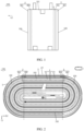
- FIG. 1 is a schematic diagram of the interior of an electrochemical device 100 according to each embodiment of this application.
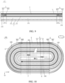
- FIG. 2 is a schematic diagram of an electrochemical device according to Embodiment 1 of this application.
- the electrochemical device 100 includes: an electrode assembly 1, a housing 2, a first bonding piece 3, a second bonding piece 4, and a third bonding piece 5.
- the electrode assembly 1 is accommodated in the housing 2.
- the first bonding piece 3, the second bonding piece 4, and the third bonding piece 5 are all disposed between the electrode assembly 1 and the housing 2.
- the electrode assembly 1 includes a first electrode plate 11, a second electrode plate 12, and a separator 13 disposed between the first electrode plate 11 and the second electrode plate 12.
- the first electrode plate 11, the separator 13, and the second electrode plate 12 are wound to form a wound structure.
- the electrode assembly 1 includes a first section 101, a first bend section 102, a second section 103, and a second bend section 104 that are connected in sequence.
- the first electrode plate 11, the separator 13, and the second electrode plate 12 are wound around a winding center axis C2 along the winding direction C1 to form a wound structure.
- first section 101 and the second section 103 may be flat straight sections that are parallel to each other. In some embodiments, the first section 101 and/or the second section 103 may be bend sections instead, without being particularly limited herein.
- each component in this application is a thickness direction L1 of the electrode assembly 1.
- the direction from the first bend section 102 to the second bend section 104 is defined as a width direction L2 of the electrode assembly 1.
- the directions defined in this application are merely for ease of description, without constituting any limitation on this application.
- the first electrode plate 11 and the second electrode plate 12 are of opposite polarities.
- the first electrode plate 11 is a positive electrode plate, and the second electrode plate 12 is a negative electrode plate; or, the first electrode plate 11 is a negative electrode plate, and the second electrode plate 12 is a positive electrode plate.
- the housing 2 is a packaging bag formed by a packaging film configured to package the electrode assembly 1.
- the packaging film is an aluminum plastic film.
- the electrochemical device 100 forms a pouch-type battery.
- the housing 2 may be a steel shell or an aluminum shell instead.
- the electrochemical device 100 forms a hard-case battery, such as a steel-case battery or an aluminum-case battery, without being particularly limited herein.
- the first bonding piece 3 includes a first body portion 301 and a first extension portion 302.
- the first body portion 301 is configured to bond the first bend section 102 to the housing 2.
- the first extension portion 302 extends from the first body portion 301 to the surface of the first section 101 along a direction opposite to the winding direction C1.
- the second bonding piece 4 includes a second body portion 401 and a second extension portion 402.
- the second body portion 401 is configured to bond the second bend section 104 to the housing 2.
- the second extension portion 402 extends from the second body portion 401 to the surface of the first section 101 along the winding direction C1.
- the third bonding piece 5 is disposed between the electrode assembly 1 and the housing 2.
- the third bonding piece 5 is bonded to the housing 2, the first extension portion 302, and the second extension portion 402.
- a part to which the third bonding piece 5 is bonded on the housing 2 is a part corresponding to the first section 101 on the housing 2.
- first bonding piece 3, the second bonding piece 4, and the third bonding piece 5 may be discrete structures or an integrated structure.
- first bonding piece 3, the second bonding piece 4, and the third bonding piece 5 may be a one-piece structure, without being particularly limited herein.
- the material thereof includes polyamide (PA), polyester (PES), polyethylene (PE), polypropylene (PP), polyesteramide (PEA), polyurethane (PU), styrene and a block copolymer thereof, ethylene-propylene-1-butene polymer (APAO), poly(ethylene-co-vinyl acetate) (EVA), poly(ethylene-co-ethyl acrylate) (EEA), poly(ethylene-co-acrylic acid) (EAA), or the like.
- PA polyamide
- PET polyethylene
- PP polypropylene
- PET polyesteramide
- PU polyurethane
- PU polyurethane
- styrene and a block copolymer thereof ethylene-propylene-1-butene polymer
- APAO ethylene-propylene-1-butene polymer
- EVA poly(ethylene-co-vinyl acetate)
- EAA poly(ethylene-co-ethyl acrylate)
- EAA poly(ethylene
- the housing 2 is bonded to the electrode assembly 1 by the first bonding piece 3 and the second bonding piece 4, thereby reducing the wobbling of the electrode assembly 1 in the housing 2, and improving the anti-drop performance of the electrochemical device 100.
- the housing 2 is bonded to the third bonding piece 5.
- the third bonding piece 5 is further bonded to the first extension portion 302 of the first bonding piece 3.
- the third bonding piece 5 is further bonded to the second extension portion 402 of the second bonding piece 4, thereby reducing the wobbling of the electrode assembly 1 in the housing 2, and improving the anti-drop performance of the electrochemical device 100.
- the stress is cushioned by the first bonding piece 3, the second bonding piece 4, and the third bonding piece 5, thereby reducing the risk of tearing and damaging the electrode assembly 1, and reducing the risk of failure of the electrochemical device 100.
- the stress on the housing 2 is transmitted to the first bonding piece 3 and the second bonding piece 4 through the third bonding piece 5, thereby reducing the risk of tearing the electrode assembly 1 by an excessive stress between the third bonding piece 5 and the housing 2, and in turn, reducing the risk of failure of the electrochemical device 100.
- an electrolyte solution may reduce the bonding force of the third bonding piece 5 infiltrated by the electrolytic solution, and impact the third bonding piece 5 when the electrode assembly is dropping. The impact may further reduce the bonding force of the third bonding piece.
- the arrangement of the first bonding piece 3 and the second bonding piece 4 may reduce the risk of wobbling the electrode assembly 1 in the housing 2 caused by the reduced bonding force of the third bonding piece 5, and improve the safety performance.
- FIG. 3 is a schematic diagram of an electrochemical device according to Embodiment 2 of this application
- FIG. 4 is a close-up view of a part e1 shown in FIG. 3 according to an embodiment of this application.
- the first bonding piece 3 includes a first bonding layer 31, a first substrate layer 32, and a second bonding layer 33 that are stacked in sequence.
- the first bonding layer 31 is provided on the first body portion 301.
- the second bonding layer 33 is provided on the first body portion 301.
- the first bonding layer 31 is configured to bond a surface of the first substrate layer 32 oriented away from the electrode assembly 1 to the housing 2.
- the second bonding layer 33 is configured to bond a surface of the first substrate layer 32 oriented toward the electrode assembly 1 to the first bend section 102.
- the surface of the first substrate layer 32 oriented toward the electrode assembly 1 is in contact with the first section 101.
- the first substrate layer 32 is located on the first body portion 301, and extends from the first body portion 301 to the first extension portion 302.
- the first bonding layer 31 is further provided on the first extension portion 302, and the first bonding layer 31 is configured to bond the surface of the first substrate layer away from the electrode assembly 1 to a surface of the third bonding piece 5 oriented toward the electrode assembly 1.
- the second bonding layer 33 is further provided on the first extension portion 302, and the second bonding layer 33 is configured to bond the first substrate layer 32 to the electrode assembly 1.
- the first substrate layer 32 extends from the first body portion 301 to the first extension portion 302
- the second bonding layer 33 extends from the first body portion 301 to the first extension portion 302
- the second bonding layer 33 is configured to bond the first substrate layer 32 to the first section 101 of the electrode assembly 1, and the first bonding layer 31 is fully located on the first body portion 301.
- the first bonding layer 31 extends to the first extension portion 302, but a part of the first substrate layer 32, which is located on the first extension portion 302, is exposed to allow for bonding between the third bonding piece 5 and the first extension portion 302 of the first bonding piece 3. In this way, the size of the electrode assembly 1 in the thickness direction L1 of the electrode assembly 1 is prevented from being increased by the bonding between the first bonding piece 3 and the third bonding piece 5.
- the size of the first bonding layer 31 is not less than 10 mm, so as to ensure proper connection between the first bonding piece 3 and the housing 2.
- the material of the first substrate layer 32 includes at least one of polyfluoroolefin, polyethylene terephthalate (PET), polyimide (PI), polyamideimide (PAI), a heat-shrinkable material, polyvinyl chloride (PVC), or a biaxially oriented polyolefin (POF) heat-shrinkable film.
- the polyfluoroolefin may be, but without being limited to, polytetrafluoroethylene or polyvinylidene difluoride.
- the first substrate layer 32 may be made of a metal instead, such as aluminum, copper or stainless steel.
- the materials of the first bonding layer 31 and the second bonding layer 33 include at least one of acrylic resin, polyurethane/rubber, or silicone.
- the acrylic resin may be, but without being limited to, ethyl 2-methylacrylate (EBN).
- the first bonding layer 31 may be a hot-melt adhesive, thereby making it convenient to put the electrode assembly 1 into the housing 2. In a hot pressing process, the first bonding layer 31 is bonded to the housing 2.
- the thickness of the first substrate layer 32 is greater than the thickness of the first bonding layer 31, and the thickness of the first substrate layer 32 is greater than the thickness of the second bonding layer 33.
- the thickness of the first bonding piece 3 ranges from 20 ⁇ m to 48 ⁇ m.
- the thickness of the first bonding layer 31 ranges from 4 ⁇ m to 15 ⁇ m.
- the thickness of the second bonding layer 33 ranges from 4 ⁇ m to 15 ⁇ m.
- the thickness of the first substrate layer 32 ranges from 10 ⁇ m to 20 ⁇ m.
- FIG. 5 is a schematic diagram of an electrochemical device according to Embodiment 3 of this application.
- FIG. 6 is a close-up view of a part e2 shown in FIG. 5 according to an embodiment of this application.
- the second bonding piece 4 includes a third bonding layer 41, a second substrate layer 42, and a fourth bonding layer 43 that are stacked in sequence.
- the third bonding layer 41 is provided on the second body portion 401.
- the fourth bonding layer 43 is provided on the second body portion 401.
- the third bonding layer 41 is configured to bond a surface of the second substrate layer 42 oriented away from the electrode assembly 1 to the housing 2.
- the fourth bonding layer 43 is configured to bond a surface of the second substrate layer 42 oriented toward the electrode assembly 1 to the first bend section 102.
- the surface of the second substrate layer 42 oriented toward the electrode assembly 1 is in contact with the first section 101.
- the second substrate layer 42 is located on the second body portion 401, and extends from the second body portion 401 to the second extension portion 402.
- the third bonding layer 41 is further provided on the second extension portion 402. The third bonding layer 41 is configured to bond the surface of the second substrate layer 42 oriented away from the electrode assembly 1 to the surface of the third bonding piece 5 oriented toward the electrode assembly 1.
- the fourth bonding layer 43 is further provided on the second extension portion 402. The fourth bonding layer 43 is configured to bond the second substrate layer 42 to the electrode assembly 1.
- the second substrate layer 42 extends from the second body portion 401 to the second extension portion 402
- the fourth bonding layer 43 extends from the second body portion 401 to the second extension portion 402
- the fourth bonding layer 43 is configured to bond the second substrate layer 42 to the first section 101 of the electrode assembly 1, and the third bonding layer 41 is fully located on the second body portion 401.
- the third bonding layer 41 extends to the second extension portion 402, but a part of the second substrate layer 42, which is located on the second extension portion 402, is exposed to allow for bonding between the third bonding piece 5 and the second extension portion 402 of the second bonding piece 4. In this way, the size of the electrode assembly 1 in the thickness direction L1 of the electrode assembly 1 is prevented from being increased by the bonding between the second bonding piece 4 and the third bonding piece 5.
- the size of the third bonding layer 41 is not less than 10 mm, so as to ensure proper connection between the second bonding piece 4 and the housing 2.
- the material of the second substrate layer 42 includes at least one of polyfluoroolefin, polyethylene terephthalate (PET), polyimide (PI), polyamideimide (PAI), a heat-shrinkable material, polyvinyl chloride (PVC), or a biaxially oriented polyolefin (POF) heat-shrinkable film.
- the polyfluoroolefin may be, but without being limited to, polytetrafluoroethylene or polyvinylidene difluoride.
- the second substrate layer 42 may be made of a metal instead, such as aluminum, copper or stainless steel.
- the materials of the third bonding layer 41 and the fourth bonding layer 43 include at least one of acrylic resin, polyurethane/rubber, or silicone.
- the acrylic resin may be, but without being limited to, ethyl 2-methylacrylate (EBN).
- the third bonding layer 41 may be a hot-melt adhesive, thereby making it convenient to put the electrode assembly 1 into the housing 2. In a hot pressing process, the third bonding layer 41 is bonded to the housing 2.
- the thickness of the second substrate layer 42 is greater than the thickness of the third bonding layer 41, and the thickness of the second substrate layer 42 is greater than the thickness of the fourth bonding layer 43.
- the thickness of the first bonding piece 3 ranges from 20 ⁇ m to 48 ⁇ m.
- the thickness of the third bonding layer 41 ranges from 4 ⁇ m to 15 ⁇ m.
- the thickness of the fourth bonding layer 43 ranges from 4 ⁇ m to 15 ⁇ m.
- the thickness of the second substrate layer 42 ranges from 10 ⁇ m to 20 ⁇ m.
- Embodiment 3 may be combined with Embodiment 2, and a technical solution thereby formed still falls within the protection scope of this application.
- FIG. 7 is a schematic diagram of an electrochemical device according to Embodiment 4 of this application.
- FIG. 8 is a close-up view of a part e3 shown in FIG. 7 according to an embodiment of this application.
- the third bonding piece 5 includes a fifth bonding layer 51 and a third substrate layer 52 that are stacked together.
- the fifth bonding layer 51 is configured to bond a surface of the third substrate layer 52 oriented away from the electrode assembly 1 to the housing 2.
- the surface of the third substrate layer 52 oriented toward the electrode assembly 1 is bonded to the first extension portion 302 of the first bonding piece 3.
- the surface of the third substrate layer 52 oriented toward the electrode assembly 1 is also bonded to the second extension portion 402.
- the third bonding piece 5 not only includes the fifth bonding layer 51 and the third substrate layer 52, but also includes a sixth bonding layer 53.
- the sixth bonding layer 53 is configured to bond the surface of the third substrate layer 52 oriented toward the electrode assembly 1 to the first extension portion 302 of the first bonding piece 3.
- the sixth bonding layer 53 is further configured to bond the surface of the third substrate layer 52 oriented toward the electrode assembly 1 to the second extension portion 402 of the second bonding piece 4.
- a part of the surface of the third substrate layer 52 oriented toward the electrode assembly 1 corresponding to the electrode assembly 1 is defined as a first part 521.
- the area of the first part 521 is S1.
- the area of the sixth bonding layer 53 provided on the first part 521 is S2.
- the areas satisfy 0 ⁇ S2/S1 ⁇ 0.1. Therefore, the third substrate layer 52 is not bonded to the electrode assembly 1 or a small part of the third substrate layer 52 is bonded to the electrode assembly 1. In this way, when the stress on the housing 2 is transmitted to the third bonding piece 5, the stress may be transmitted quickly to the first bonding layer 31 and the second bonding layer 33 to reduce the risk of damaging the electrode assembly 1 corresponding to the third bonding layer 41.
- Embodiment 4 may be combined with Embodiment 2 and/or Embodiment 3, and a technical solution thereby formed still falls within the protection scope of this application.
- FIG. 9 is a close-up view of a part e4 shown in FIG. 2 according to an embodiment of this application.
- This embodiment further defines the width of the first extension portion 302 in Embodiment 1.
- the width d1 of the first extension portion 302 is 4 mm to 15 mm.
- This embodiment further defines the width of the second extension portion 402 in Embodiment 1.
- the width d2 of the second extension portion 402 is 4 mm to 15 mm.
- Embodiment 5 may be combined with one or more of Embodiment 2, Embodiment 3, and Embodiment 4, and a technical solution thereby formed still falls within the protection scope of this application.
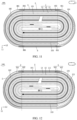
- FIG. 10 is a schematic diagram of an electrochemical device according to Embodiment 6 of this application.
- the electrochemical device 100 includes a first tab 6.
- the first tab 6 is connected to the first electrode plate 11.
- the first tab 6 is distant from the first extension portion 302, and the first tab 6 is distant from the second extension portion 402.
- the thickness of the electrode assembly 1 may be prevented from being increased by the bonding between the third bonding piece 5 and the first extension portion 302 or second extension portion 402.
- the electrochemical device 100 includes a second tab 7.
- the second tab 7 is connected to the second electrode plate 12.
- the second tab 7 is distant from the first extension portion 302, and the second tab 7 is distant from the second extension portion 402.
- the thickness of the electrode assembly 1 may be prevented from being increased by the bonding between the third bonding piece 5 and the first extension portion 302 or second extension portion 402.
- Embodiment 6 may be combined with one or more of Embodiment 2, Embodiment 3, Embodiment 4, or Embodiment 5, and a technical solution thereby formed still falls within the protection scope of this application.
- FIG. 11 is a schematic diagram of an electrochemical device according to Embodiment 7 of this application.
- This embodiment differs from Embodiment 1 in that the first bonding piece 3 includes a third extension portion 303 in addition to the first body portion 301 and the first extension portion 302, and the third extension portion 303 extends from the first body portion 301 to the surface of the second section 103 along the winding direction C1.
- the second bonding piece 4 includes a fourth extension portion 403 in addition to the second body portion 401 and the second extension portion 402. The fourth extension portion 403 extends from the second body portion 401 to the surface of the second section 103 along a direction opposite to the winding direction C1.
- the electrochemical device 100 further includes a fifth bonding piece 8.
- the fifth bonding piece 8 is disposed between the electrode assembly 1 and the housing 2.
- the fifth bonding piece 8 is bonded to the housing 2, the third extension portion 303, and the fourth extension portion 403.
- a part to which the fifth bonding piece 8 is bonded on the housing 2 is a part corresponding to the second section 103 on the housing 2.
- the arrangement of the third extension portion 303, the fourth extension portion 403, and the fifth bonding piece 8 reduces the wobbling of the electrode assembly 1 in the housing 2, and improves the anti-drop performance of the electrochemical device 100.
- the structure and functions of the fifth bonding piece 8 may be learned by referring to the description of the third bonding piece 5 in Embodiment 4, details of which are omitted here.
- Embodiment 5 and Embodiment 6 may be combined with this embodiment, and a technical solution thereby formed still falls within the protection scope of this application.
- FIG. 12 is a schematic diagram of an electrochemical device according to Embodiment 8 of this application. This embodiment further defines the wound structure in Embodiment 1.
- the first electrode plate 11 includes a first current collector 111, and an outer surface of the first section 101 is an outer surface of the first current collector 111.
- the outer surface of the first section 101 is a surface of a part farthest from the winding center axis C2 on the first section 101, where the surface is oriented away from the winding center axis C2.
- the outer surface of the first section 101 is the first current collector 111 in the first electrode plate 11 rather than the separator 13.
- the first electrode plate 11 is a positive electrode plate, such an arrangement increases the capacity of the electrode assembly 1.
- the first current collector 111 increases the hardness of the electrode assembly 1, thereby enhancing the protection for the electrode assembly 1.
- the outer surface of the first section 101 is the outer surface of the first current collector 111, but also the outermost layer of the second bend section 104 is the separator 13.
- An ending 131 of the separator 13 is located on the second bend section 104. Because the second bonding piece 4 is bonded to the second bend section 104, the second bonding piece 4 may serve as a finishing adhesive to bond the ending 131 of the separator 13 to the second bend section 104.
- the electrochemical device 100 when the electrochemical device 100 is applied to an electronic device, a part corresponding to the first section 101 or second section 103 on the housing 2 is bonded to the interior of the electronic device. Therefore, when the electronic device is subjected to mechanical abuse such as drop, collision, and vibration, the part corresponding to the first section 101 or second section 103 on the housing 2 is pulled by the electronic device. In other words, the part corresponding to the first section 101 or second section 103 on the housing 2 is stressed.
- the outer surface of the first section 101 is the outer surface of the first current collector 111
- the ending 131 of the separator 13 is disposed on the second bend section 104
- the first bonding piece 3, the second bonding piece 4, and the third bonding piece 5 are disposed.
- the stress is transmitted from the third bonding piece 5 to the first bonding piece 3 and the second bonding piece 4.
- the stress is transferred to the unstressed or less stressed first bend section 102 and second bend section 104, thereby improving the protection for the first section 101 and second section 103 of the electrode assembly 1 and reducing the risk of failure of the electrochemical device 100 stressed on the whole.
- Embodiment 8 may be combined with one or more of Embodiment 2, Embodiment 3, Embodiment 4, or Embodiment 5, Embodiment 6, or Embodiment 7, and a technical solution thereby formed still falls within the protection scope of this application.
- Experimental Example 1 and Experimental Example 2 have the same structure, and employ the electrochemical device in Embodiment 5.
- the width of the first extension portion is 5 mm, and the width of the second extension portion is 5 mm.
- Experimental Example 1 differs from Experimental Example 2 in the size. Specifically, along the length direction of the electrode assembly, the length of the electrochemical device in Experimental Example 1 is 90 mm. Along the width direction of the electrode assembly, the width of the electrochemical device in Experimental Example 1 is 66 mm. Along the thickness direction of the electrode assembly, the thickness of the electrochemical device in Experimental Example is 6 mm. The length direction of the electrode assembly is perpendicular to the width direction of the electrode assembly and the thickness direction of the electrode assembly. Along the length direction of the electrode assembly, the length of the electrochemical device in Experimental Example 2 is 87 mm. Along the width direction of the electrode assembly, the width of the electrochemical device in Experimental Example 2 is 64 mm. Along the thickness direction of the electrode assembly, the thickness of the electrochemical device in Experimental Example 2 is 4.8 mm.
- Comparative Example 1 and Comparative Example 2 Two types of electrochemical devices in the prior art are used as comparative embodiments: Comparative Example 1 and Comparative Example 2.
- Comparative Example 1 and Comparative Example 2 have the same structure that includes an electrode assembly and a housing. The electrode assembly is accommodated in the housing. A bonding piece is disposed between the electrode assembly and the housing. The bonding piece corresponds to the first section of the electrode assembly.
- Comparative Example 1 and Comparative Example 2 include neither the first bonding piece nor the second bonding piece.
- Comparative Example 1 is given in contrast to Experimental Example 1, and the size of the electrochemical device in Comparative Example 1 is the same as that in Experimental Example 1.
- Comparative Embodiment 2 is given in contrast to Experimental Example 2, and the size of the electrochemical device in Comparative Embodiment 2 is the same as that in Experimental Example 2.
- the performance test includes a drop test.
- Table 1 records the number of electrochemical devices with the first electrode plate being torn, the number of the electrochemical devices with a ruptured housing, and the number of short-circuited and failed electrochemical devices among 10 electrochemical devices subjected to a drop test.
- the process of the drop test is: Dropping an electrochemical device freely to the surface of a steel plate from a height of 1.8 meters for 6 times in 1 round until 3 rounds are completed. In each round, letting two surfaces of the electrochemical device along the thickness direction of the electrode assembly fall downward to the steel plate respectively, and letting 4 corners of the electrochemical device fall downward to the steel plate respectively.
- Table 1 Number with torn first electrode plate Number with ruptured housing Number of short-circuited and failed electrochemical devices Comparative Example 1 8 5 7 Experimental Example 1 0 0 2 Comparative Example 2 6 4 6 Experimental Example 2 0 0 0
- the anti-drop performance of the electrochemical device of the Experimental Example is higher than that of the Comparative Examples, indicating that the anti-drop performance of the electrochemical device according the Experimental Example of this application is improved significantly.
- the electrochemical devices according to the Experimental Example of this application may reduce the failure caused by reasons such as an external force.
- FIG. 13 is a schematic diagram of an electronic device according to an embodiment of this application.
- the electronic device 200 includes a main body 201 and the electrochemical device 100 according to any one of Embodiments 1 to 8 described above.
- the specific structure and functions of the electrochemical device 100 may be learned by referring to the foregoing embodiments, details of which are omitted here.
- the electronic device 200 further includes a fourth bonding piece 202.
- the fourth bonding piece 202 is configured to bond the main body 201 to the housing 2.
- the third bonding piece 5 is located between the first section 101 and the fourth bonding piece 202.
- the electrochemical device 100 is disposed inside the electronic device, thereby reducing the wobbling of the electrochemical device 100.
- the stress can be transmitted to the first bonding piece 3 and the second bonding piece 4 through the fourth bonding piece 202 and the third bonding piece 5. In this way, the stress is dispersed, the failure of the electrochemical device 100 is reduced, and the service life of the electronic device 200 is increased.
Landscapes
- Chemical & Material Sciences (AREA)
- Chemical Kinetics & Catalysis (AREA)
- Electrochemistry (AREA)
- General Chemical & Material Sciences (AREA)
- Engineering & Computer Science (AREA)
- Manufacturing & Machinery (AREA)
- Connection Of Batteries Or Terminals (AREA)
- Electric Double-Layer Capacitors Or The Like (AREA)
- Sealing Battery Cases Or Jackets (AREA)
- Secondary Cells (AREA)
Abstract
Description
- Embodiments of this application relate to the technical field of energy storage.
- An electrochemical device is a device that converts external energy into electrical energy and stores the electrical energy internally so that the electrical energy can be supplied to an external electronic device (such as a portable electronic device) when necessary. Currently, electrochemical devices are widely used in electronic devices such as a notebook computer, an e-book player, a portable phone, a portable fax machine, a video recorder, an LCD television set, a portable cleaner, a backup power supply, an automobile, a motorcycle, a bicycle, a lighting device, a game console, a watch or clock, a large household battery, and a capacitor. Safety performance of the electrochemical devices is of concern to users.
- In a process of implementing this application, the applicant hereof finds that during the transportation or use of an electronic device, mechanical abuse such as drop, collision, and vibration often occurs, so that a housing of the electrochemical device is prone to be stressed. The stress transmitted into the electrochemical device causes partial tearing of the interior of the electrochemical device, resulting in failure of the electrochemical device.
- In view of the foregoing problems, embodiments of this application provide an electrochemical device and an electronic device to overcome or at least partly solve the foregoing problem of failure of the electrochemical device.
- According to an aspect of embodiments of this application, an electrochemical device is provided. The electrochemical device includes an electrode assembly, a housing, a first bonding piece, a second bonding piece, and a third bonding piece. The electrode assembly includes a first electrode plate, a second electrode plate, and a separator disposed between the first electrode plate and the second electrode plate. The first electrode plate, the separator, and the second electrode plate are wound to form a wound structure. Along a winding direction, the electrode assembly includes a first section, a first bend section, a second section, and a second bend section that are connected in sequence. The housing is configured to accommodate the electrode assembly. The first bonding piece includes a first body portion disposed on a surface of the first bend section and a first extension portion disposed on a surface of the first section. The first body portion is configured to bond the first bend section to the housing. The second bonding piece includes a second body portion disposed on a surface of the second bend section and a second extension portion disposed on the surface of the first section. The second body portion is configured to bond the second bend section to the housing. The third bonding piece is disposed between the electrode assembly and the housing. The third bonding piece is bonded to the housing, the first extension portion, and the second extension portion.
- The housing is bonded to the electrode assembly by the first bonding piece and the second bonding piece, thereby reducing the wobbling of the electrode assembly in the housing, and improving the anti-drop performance of the electrochemical device. The housing is bonded to the third bonding piece, and the third bonding piece is further bonded to the first extension portion of the first bonding piece and bonded to the second extension portion of the second bonding piece, thereby reducing the wobbling of the electrode assembly in the housing, and improving the anti-drop performance of the electrochemical device. When the housing is stressed, on the one hand, the stress is cushioned by the first bonding piece, the second bonding piece, and the third bonding piece, thereby reducing the risk of tearing and damaging the electrode assembly, and reducing the risk of failure of the electrochemical device. On the other hand, the stress on the housing is transmitted to the first bonding piece and the second bonding piece through the third bonding piece, thereby reducing the risk of tearing the electrode assembly by an excessive stress between the third bonding piece and the housing. In addition, an electrolyte solution may reduce the bonding force of the third bonding piece infiltrated by the electrolyte solution, and impact the third bonding piece when the electrode assembly is dropping. The impact may further reduce the bonding force of the third bonding piece. The arrangement of the first bonding piece and the second bonding piece may reduce the risk of the wobbling the electrode assembly in the housing, and improve the safety performance.
- In some embodiments, the first section and the second section are flat straight sections that are parallel to each other. In some embodiments, the first section and/or the second section are bend sections. In some embodiments, a direction from the first section to the second section is a thickness direction of the electrode assembly. In some embodiments, a direction from the first bend section to the second bend section is a width direction of the electrode assembly.
- In some embodiments, the first electrode plate and the second electrode plate are of opposite polarities. The first electrode plate is a positive electrode plate, and the second electrode plate is a negative electrode plate; or the first electrode plate is a negative electrode plate, and the second electrode plate is a positive electrode plate.
- In some embodiments, the housing is a packaging bag formed by a packaging film configured to package the electrode assembly. For example, the packaging film is an aluminum plastic film. In this case, the electrochemical device forms a pouch-type battery. In some embodiments, the housing is a steel shell or an aluminum shell. In this case, the electrochemical device forms a hard-case battery, such as a steel-case battery or an aluminum-case battery.
- In some embodiments, the first bonding piece, the second bonding piece, and the third bonding piece are an integrated structure. That is, the first bonding piece, the second bonding piece, and the third bonding piece are a one-piece structure.
- In some embodiments, the first bonding piece includes a first bonding layer, a first substrate layer, and a second bonding layer that are stacked in sequence. The first bonding layer is provided on the first body portion and is configured to bond a surface of the first substrate layer oriented away from the electrode assembly to the housing. The second bonding layer is provided on the first body portion and is configured to bond a surface of the first substrate layer oriented toward the electrode assembly to the first bend section. In this way, the first bonding piece implements connection between the first bend section and the housing, thereby reducing the wobbling of the electrode assembly in the housing.
- In some embodiments, the first bonding layer is further provided on the first extension portion and is configured to bond the surface of the first substrate layer oriented away from the electrode assembly to a surface of the third bonding piece oriented toward the electrode assembly.
- In some embodiments, the second bonding layer is further provided on the first extension portion and is configured to bond the first substrate layer to the electrode assembly.
- In some embodiments, the surface of the first substrate layer oriented toward the electrode assembly is in contact with the first section. That is, the first substrate layer is located in the first body portion and extends from the first body portion to the first extension portion, thereby making it convenient for the first bonding piece and the third bonding piece to bond.
- In some embodiments, the second bonding piece includes a third bonding layer, a second substrate layer, and a fourth bonding layer that are stacked in sequence. The third bonding layer is provided on the second body portion and is configured to bond the second substrate layer to the housing. The fourth bonding layer is provided on the second body portion and is configured to bond the second substrate layer to the second bend section. The third bonding layer and the fourth bonding layer make it convenient to bond the second bonding piece to the housing and the second bend section, and reduce the wobbling of the electrode assembly in the housing.
- In some embodiments, the third bonding layer is further provided on the second extension portion and is configured to bond the second substrate layer to the third bonding piece.
- In some embodiments, the fourth bonding layer is further provided on the second extension portion and is configured to bond the second substrate layer to the first section.
- In some embodiments, the surface of the second substrate layer oriented toward the electrode assembly is in contact with the first section. That is, the second substrate layer is located in the second body portion and extends from the second body portion to the second extension portion, thereby making it convenient for the second bonding piece and the third bonding piece to bond.
- In some embodiments, at least one of the first bonding piece, the second bonding piece, or the third bonding piece is a hot-melt adhesive.
- In some embodiments, the third bonding piece includes a fifth bonding layer and a third substrate layer that are stacked together. The fifth bonding layer is configured to bond a surface of the third substrate layer oriented away from the electrode assembly to the housing. A surface of the third substrate layer oriented toward the electrode assembly is bonded to the first extension portion and the second extension portion.
- In some embodiments, the third bonding piece includes a fifth bonding layer, a third substrate layer, and a sixth bonding layer that are stacked in sequence. The fifth bonding layer is configured to bond a surface of the third substrate layer oriented away from the electrode assembly to the housing. The sixth bonding layer is configured to bond a surface of the third substrate layer oriented toward the electrode assembly to the first extension portion. The sixth bonding layer is further configured to bond the surface of the third substrate layer oriented toward the electrode assembly to the second extension portion. The fifth bonding layer and the sixth bonding layer enable the third bonding piece to bond to the housing, the first extension portion of the first bonding piece, and the second extension portion of the second bonding piece.
- In some embodiments, in a thickness direction of the electrode assembly, a part of the surface of the third substrate layer oriented toward the electrode assembly corresponding to the electrode assembly is defined as a first part, an area of the first part is
S 1, an area of the sixth bonding layer provided on the first part is S2, 0 < S2/S 1 ≤ 0.1. So the third substrate layer is not bonded to the electrode assembly or a part of the third substrate layer is bonded to the electrode assembly. In this way, when the stress on the housing is transmitted to the third bonding piece, the stress can be transmitted quickly to the first bonding layer and the second bonding layer to reduce the risk of damaging the electrode assembly corresponding to the third bonding layer. - In some embodiments, along the winding direction, a width of the first extension portion is 4 mm to 15 mm.
- In some embodiments, along the winding direction, a width of the second extension portion is 4 mm to 15 mm.
- In some embodiments, the first electrode plate includes a first current collector, and an outer surface of the first section is an outer surface of the first current collector. Generally, the hardness of the first current collector is greater than the hardness of the separator. By disposing the first current collector on the outer surface of the first section, the protection for the electrode assembly is enhanced.
- In some embodiments, an outermost layer of the second bend section is the separator, and an ending of the separator is located in the second bend section. When the part corresponding to the first section on the housing is stressed, the stress can be transmitted from the third bonding piece to the first bonding piece and the second bonding piece. In other words, the stress is transmitted to the unstressed or less stressed first bend section and second bend section, thereby enhancing the protection for the electrode assembly corresponding to the first section, and reducing the risk of failure of the electrochemical device that is stressed on the whole.
- In some embodiments, the first electrode plate is a positive electrode plate. When the first electrode plate is located at the outermost circle of the winding structure, in contrast to a circumstance in which the first electrode plate is a negative electrode plate, the electrode assembly achieves a higher capacity and a higher energy density.
- In some embodiments, the electrochemical device includes a first tab. The first tab is connected to the first electrode plate. In a width direction of the electrode assembly, the first tab is detached from the first extension portion, and the first tab is detached from the second extension portion. In this way, in the thickness direction of the electrode assembly, the thickness of the electrode assembly is prevented from being increased by the bonding between the third bonding piece and the first extension portion or second extension portion.
- In some embodiments, the first bonding piece includes a third extension portion in addition to the first body portion and the first extension portion. The third extension portion extends from the first body portion to the surface of the second section along the winding direction. The second bonding piece includes a fourth extension portion in addition to the second body portion and the second extension portion. The fourth extension portion extends from the second body portion to the surface of the second section along a direction opposite to the winding direction. The electrochemical device further includes a fifth bonding piece. The fifth bonding piece is disposed between the electrode assembly and the housing. The fifth bonding piece is bonded to the housing, the third extension portion, and the fourth extension portion. The arrangement of the third extension portion, the fourth extension portion, and the fifth bonding piece enhances the protection for the electrode assembly.
- According and an aspect of embodiments of this application, this application provides an electronic device. The electronic device includes a main body and the electrochemical device described above.
- In some embodiments, the electronic device further includes a fourth bonding piece. The fourth bonding piece is configured to bond the main body to the housing. In a thickness direction of the electrode assembly, the third bonding piece is located between the first section and the fourth bonding piece. In this way, the electrochemical device is disposed inside the electronic device, thereby reducing the wobbling of the electrochemical device. In addition, when the part corresponding to the first section on the housing of the electrochemical device is subjected to a stress from the electronic device or the like, the stress can be transmitted to the first bonding piece and the second bonding piece through the fourth bonding piece and the third bonding piece. In this way, the stress is dispersed, the risk of failure of the electrochemical device is reduced, and the service life of the electronic device is increased.
- The beneficial effects of embodiments of this application include: an electrochemical device is provided, and a first bonding piece, a second bonding piece, and a third bonding piece are disposed between the electrode assembly and the housing of the electrochemical device. The first bonding piece is configured to bond the first bend section of the electrode assembly to the housing. The second bonding piece is configured to bond the second bend section of the electrode assembly to the housing. The third bonding piece is bonded to the first bonding piece and the second bonding piece, and the third bonding piece is bonded to the housing, thereby reducing the wobbling of the electrode assembly in the housing, and improving the anti-drop performance of the electrochemical device. When the housing is stressed, on the one hand, the stress is cushioned by the first bonding piece, the second bonding piece, and the third bonding piece, thereby reducing the risk of tearing and damaging the electrode assembly, and reducing the risk of failure of the electrochemical device. On the other hand, the stress on the housing is transmitted to the first bonding piece and the second bonding piece through the third bonding piece, thereby reducing the risk of tearing the electrode assembly by an excessive stress between the third bonding piece and the housing, and in turn, reducing the risk of failure of the electrochemical device. In addition, an electrolyte solution may reduce the bonding force of the third bonding piece infiltrated by the electrolytic solution, and impact the third bonding piece when the electrode assembly is dropping. The impact may further reduce the bonding force of the third bonding piece. The arrangement of the first bonding piece and the second bonding piece may reduce the risk of wobbling the electrode assembly in the housing caused by the reduced bonding force of the third bonding piece, and improve the safety performance.
- One or more embodiments are described illustratively with reference to drawings corresponding to the embodiments. The illustrative description does not constitute any limitation on the embodiments. Components marked with the same reference numeral in the drawings represent similar components. Unless otherwise specified, the drawings do not constitute any scale limitation.
-
FIG. 1 is a schematic diagram of the interior of an electrochemical device according to each embodiment of this application; -
FIG. 2 is a schematic diagram of an electrochemical device according toEmbodiment 1 of this application; -
FIG. 3 is a schematic diagram of an electrochemical device according toEmbodiment 2 of this application; -
FIG. 4 is a close-up view of a part e1 shown inFIG. 3 according to an embodiment of this application; -
FIG. 5 is a schematic diagram of an electrochemical device according toEmbodiment 3 of this application; -
FIG. 6 is a close-up view of a part e2 shown inFIG. 5 according to an embodiment of this application; -
FIG. 7 is a schematic diagram of an electrochemical device according to Embodiment 4 of this application; -
FIG. 8 is a close-up view of a part e3 shown inFIG. 7 according to an embodiment of this application; -
FIG. 9 is a close-up view of a part e4 shown inFIG. 2 according to an embodiment of this application; -
FIG. 10 is a schematic diagram of an electrochemical device according to Embodiment 6 of this application; -
FIG. 11 is a schematic diagram of an electrochemical device according to Embodiment 7 of this application; -
FIG. 12 is a schematic diagram of an electrochemical device according to Embodiment 8 of this application; and -
FIG. 13 is a schematic diagram of an electronic device according to an embodiment of this application. - For ease of understanding this application, the following describes this application in more detail with reference to drawings and specific embodiments. It is hereby noted that an element referred to herein as "fixed to" another element may directly exist on the other element, or may be fixed to the other element through one or more intermediate elements. An element referred to herein as "connected to" another element may be connected to the other element directly or through one or more intermediate elements. The terms "vertical", "horizontal", "left", "right", "in", "out" and other similar expressions used herein are merely for ease of description.
- Unless otherwise defined, all technical and scientific terms used herein have the same meanings as what is generally understood by a person skilled in the technical field of this application. The terms used in the specification of this application are merely intended to describe specific embodiments but not to limit this application. The term "and/or" used herein is intended to include any and all combinations of one or more related items preceding and following the term.
-
FIG. 1 is a schematic diagram of the interior of anelectrochemical device 100 according to each embodiment of this application.FIG. 2 is a schematic diagram of an electrochemical device according toEmbodiment 1 of this application. Theelectrochemical device 100 includes: anelectrode assembly 1, ahousing 2, afirst bonding piece 3, a second bonding piece 4, and athird bonding piece 5. Theelectrode assembly 1 is accommodated in thehousing 2. Thefirst bonding piece 3, the second bonding piece 4, and thethird bonding piece 5 are all disposed between theelectrode assembly 1 and thehousing 2. - With respect to the
electrode assembly 1, theelectrode assembly 1 includes afirst electrode plate 11, asecond electrode plate 12, and aseparator 13 disposed between thefirst electrode plate 11 and thesecond electrode plate 12. Thefirst electrode plate 11, theseparator 13, and thesecond electrode plate 12 are wound to form a wound structure. Along a winding direction C1, theelectrode assembly 1 includes afirst section 101, afirst bend section 102, asecond section 103, and asecond bend section 104 that are connected in sequence. Thefirst electrode plate 11, theseparator 13, and thesecond electrode plate 12 are wound around a winding center axis C2 along the winding direction C1 to form a wound structure. - In some embodiments, the
first section 101 and thesecond section 103 may be flat straight sections that are parallel to each other. In some embodiments, thefirst section 101 and/or thesecond section 103 may be bend sections instead, without being particularly limited herein. - The structure and functions of each component in this application are described by using an example in which the direction from the
first section 101 to thesecond section 103 is a thickness direction L1 of theelectrode assembly 1. In this application, the direction from thefirst bend section 102 to thesecond bend section 104 is defined as a width direction L2 of theelectrode assembly 1. In addition, the directions defined in this application are merely for ease of description, without constituting any limitation on this application. - The
first electrode plate 11 and thesecond electrode plate 12 are of opposite polarities. Thefirst electrode plate 11 is a positive electrode plate, and thesecond electrode plate 12 is a negative electrode plate; or, thefirst electrode plate 11 is a negative electrode plate, and thesecond electrode plate 12 is a positive electrode plate. - With respect to the
housing 2, thehousing 2 is a packaging bag formed by a packaging film configured to package theelectrode assembly 1. For example, the packaging film is an aluminum plastic film. In this case, theelectrochemical device 100 forms a pouch-type battery. Thehousing 2 may be a steel shell or an aluminum shell instead. In this case, theelectrochemical device 100 forms a hard-case battery, such as a steel-case battery or an aluminum-case battery, without being particularly limited herein. - With respect to the
first bonding piece 3, thefirst bonding piece 3 includes afirst body portion 301 and afirst extension portion 302. Thefirst body portion 301 is configured to bond thefirst bend section 102 to thehousing 2. Thefirst extension portion 302 extends from thefirst body portion 301 to the surface of thefirst section 101 along a direction opposite to the winding direction C1. - With respect to the second bonding piece 4, the second bonding piece 4 includes a
second body portion 401 and asecond extension portion 402. Thesecond body portion 401 is configured to bond thesecond bend section 104 to thehousing 2. Thesecond extension portion 402 extends from thesecond body portion 401 to the surface of thefirst section 101 along the winding direction C1. - With respect to the
third bonding piece 5, thethird bonding piece 5 is disposed between theelectrode assembly 1 and thehousing 2. Thethird bonding piece 5 is bonded to thehousing 2, thefirst extension portion 302, and thesecond extension portion 402. A part to which thethird bonding piece 5 is bonded on thehousing 2 is a part corresponding to thefirst section 101 on thehousing 2. - It is hereby noted that the
first bonding piece 3, the second bonding piece 4, and thethird bonding piece 5 may be discrete structures or an integrated structure. In other words, thefirst bonding piece 3, the second bonding piece 4, and thethird bonding piece 5 may be a one-piece structure, without being particularly limited herein. - It is hereby noted that in some embodiments, at least one of the
first bonding piece 3, the second bonding piece 4, or thethird bonding piece 5 is a hot-melt adhesive. Specifically, the material thereof includes polyamide (PA), polyester (PES), polyethylene (PE), polypropylene (PP), polyesteramide (PEA), polyurethane (PU), styrene and a block copolymer thereof, ethylene-propylene-1-butene polymer (APAO), poly(ethylene-co-vinyl acetate) (EVA), poly(ethylene-co-ethyl acrylate) (EEA), poly(ethylene-co-acrylic acid) (EAA), or the like. - In some embodiments of this application, the
housing 2 is bonded to theelectrode assembly 1 by thefirst bonding piece 3 and the second bonding piece 4, thereby reducing the wobbling of theelectrode assembly 1 in thehousing 2, and improving the anti-drop performance of theelectrochemical device 100. Thehousing 2 is bonded to thethird bonding piece 5. Thethird bonding piece 5 is further bonded to thefirst extension portion 302 of thefirst bonding piece 3. Thethird bonding piece 5 is further bonded to thesecond extension portion 402 of the second bonding piece 4, thereby reducing the wobbling of theelectrode assembly 1 in thehousing 2, and improving the anti-drop performance of theelectrochemical device 100. When thehousing 2 is stressed, on the one hand, the stress is cushioned by thefirst bonding piece 3, the second bonding piece 4, and thethird bonding piece 5, thereby reducing the risk of tearing and damaging theelectrode assembly 1, and reducing the risk of failure of theelectrochemical device 100. On the other hand, the stress on thehousing 2 is transmitted to thefirst bonding piece 3 and the second bonding piece 4 through thethird bonding piece 5, thereby reducing the risk of tearing theelectrode assembly 1 by an excessive stress between thethird bonding piece 5 and thehousing 2, and in turn, reducing the risk of failure of theelectrochemical device 100. In addition, an electrolyte solution (not shown) may reduce the bonding force of thethird bonding piece 5 infiltrated by the electrolytic solution, and impact thethird bonding piece 5 when the electrode assembly is dropping. The impact may further reduce the bonding force of the third bonding piece. The arrangement of thefirst bonding piece 3 and the second bonding piece 4 may reduce the risk of wobbling theelectrode assembly 1 in thehousing 2 caused by the reduced bonding force of thethird bonding piece 5, and improve the safety performance. -
FIG. 3 is a schematic diagram of an electrochemical device according toEmbodiment 2 of this application, andFIG. 4 is a close-up view of a part e1 shown inFIG. 3 according to an embodiment of this application. This embodiment differs fromEmbodiment 1 in that thefirst bonding piece 3 includes afirst bonding layer 31, afirst substrate layer 32, and asecond bonding layer 33 that are stacked in sequence. Thefirst bonding layer 31 is provided on thefirst body portion 301. Thesecond bonding layer 33 is provided on thefirst body portion 301. Thefirst bonding layer 31 is configured to bond a surface of thefirst substrate layer 32 oriented away from theelectrode assembly 1 to thehousing 2. Thesecond bonding layer 33 is configured to bond a surface of thefirst substrate layer 32 oriented toward theelectrode assembly 1 to thefirst bend section 102. - In some embodiments, the surface of the
first substrate layer 32 oriented toward theelectrode assembly 1 is in contact with thefirst section 101. To be specific, thefirst substrate layer 32 is located on thefirst body portion 301, and extends from thefirst body portion 301 to thefirst extension portion 302. In some embodiments, thefirst bonding layer 31 is further provided on thefirst extension portion 302, and thefirst bonding layer 31 is configured to bond the surface of the first substrate layer away from theelectrode assembly 1 to a surface of thethird bonding piece 5 oriented toward theelectrode assembly 1. In some embodiments, thesecond bonding layer 33 is further provided on thefirst extension portion 302, and thesecond bonding layer 33 is configured to bond thefirst substrate layer 32 to theelectrode assembly 1. - In some embodiments, the
first substrate layer 32 extends from thefirst body portion 301 to thefirst extension portion 302, thesecond bonding layer 33 extends from thefirst body portion 301 to thefirst extension portion 302, thesecond bonding layer 33 is configured to bond thefirst substrate layer 32 to thefirst section 101 of theelectrode assembly 1, and thefirst bonding layer 31 is fully located on thefirst body portion 301. Alternatively, thefirst bonding layer 31 extends to thefirst extension portion 302, but a part of thefirst substrate layer 32, which is located on thefirst extension portion 302, is exposed to allow for bonding between thethird bonding piece 5 and thefirst extension portion 302 of thefirst bonding piece 3. In this way, the size of theelectrode assembly 1 in the thickness direction L1 of theelectrode assembly 1 is prevented from being increased by the bonding between thefirst bonding piece 3 and thethird bonding piece 5. - In some embodiments, along the winding direction C1, the size of the
first bonding layer 31 is not less than 10 mm, so as to ensure proper connection between thefirst bonding piece 3 and thehousing 2. - In some embodiments, the material of the
first substrate layer 32 includes at least one of polyfluoroolefin, polyethylene terephthalate (PET), polyimide (PI), polyamideimide (PAI), a heat-shrinkable material, polyvinyl chloride (PVC), or a biaxially oriented polyolefin (POF) heat-shrinkable film. The polyfluoroolefin may be, but without being limited to, polytetrafluoroethylene or polyvinylidene difluoride. Thefirst substrate layer 32 may be made of a metal instead, such as aluminum, copper or stainless steel. - In some embodiments, the materials of the
first bonding layer 31 and thesecond bonding layer 33 include at least one of acrylic resin, polyurethane/rubber, or silicone. The acrylic resin may be, but without being limited to, ethyl 2-methylacrylate (EBN). In some embodiments, thefirst bonding layer 31 may be a hot-melt adhesive, thereby making it convenient to put theelectrode assembly 1 into thehousing 2. In a hot pressing process, thefirst bonding layer 31 is bonded to thehousing 2. - In some embodiments, along a direction of stacking the
first bonding layer 31, thefirst substrate layer 32, and thesecond bonding layer 33, the thickness of thefirst substrate layer 32 is greater than the thickness of thefirst bonding layer 31, and the thickness of thefirst substrate layer 32 is greater than the thickness of thesecond bonding layer 33. The thickness of thefirst bonding piece 3 ranges from 20 µm to 48 µm. The thickness of thefirst bonding layer 31 ranges from 4 µm to 15 µm. The thickness of thesecond bonding layer 33 ranges from 4 µm to 15 µm. The thickness of thefirst substrate layer 32 ranges from 10 µm to 20 µm. -
FIG. 5 is a schematic diagram of an electrochemical device according toEmbodiment 3 of this application.FIG. 6 is a close-up view of a part e2 shown inFIG. 5 according to an embodiment of this application. This embodiment differs fromEmbodiment 1 in that the second bonding piece 4 includes athird bonding layer 41, asecond substrate layer 42, and afourth bonding layer 43 that are stacked in sequence. Thethird bonding layer 41 is provided on thesecond body portion 401. Thefourth bonding layer 43 is provided on thesecond body portion 401. Thethird bonding layer 41 is configured to bond a surface of thesecond substrate layer 42 oriented away from theelectrode assembly 1 to thehousing 2. Thefourth bonding layer 43 is configured to bond a surface of thesecond substrate layer 42 oriented toward theelectrode assembly 1 to thefirst bend section 102. - In some embodiments, the surface of the
second substrate layer 42 oriented toward theelectrode assembly 1 is in contact with thefirst section 101. To be specific, thesecond substrate layer 42 is located on thesecond body portion 401, and extends from thesecond body portion 401 to thesecond extension portion 402. In some embodiments, thethird bonding layer 41 is further provided on thesecond extension portion 402. Thethird bonding layer 41 is configured to bond the surface of thesecond substrate layer 42 oriented away from theelectrode assembly 1 to the surface of thethird bonding piece 5 oriented toward theelectrode assembly 1. In some embodiments, thefourth bonding layer 43 is further provided on thesecond extension portion 402. Thefourth bonding layer 43 is configured to bond thesecond substrate layer 42 to theelectrode assembly 1. - Preferably, the
second substrate layer 42 extends from thesecond body portion 401 to thesecond extension portion 402, thefourth bonding layer 43 extends from thesecond body portion 401 to thesecond extension portion 402, thefourth bonding layer 43 is configured to bond thesecond substrate layer 42 to thefirst section 101 of theelectrode assembly 1, and thethird bonding layer 41 is fully located on thesecond body portion 401. Alternatively, thethird bonding layer 41 extends to thesecond extension portion 402, but a part of thesecond substrate layer 42, which is located on thesecond extension portion 402, is exposed to allow for bonding between thethird bonding piece 5 and thesecond extension portion 402 of the second bonding piece 4. In this way, the size of theelectrode assembly 1 in the thickness direction L1 of theelectrode assembly 1 is prevented from being increased by the bonding between the second bonding piece 4 and thethird bonding piece 5. - In some embodiments, along the winding direction C1, the size of the
third bonding layer 41 is not less than 10 mm, so as to ensure proper connection between the second bonding piece 4 and thehousing 2. - In some embodiments, the material of the
second substrate layer 42 includes at least one of polyfluoroolefin, polyethylene terephthalate (PET), polyimide (PI), polyamideimide (PAI), a heat-shrinkable material, polyvinyl chloride (PVC), or a biaxially oriented polyolefin (POF) heat-shrinkable film. The polyfluoroolefin may be, but without being limited to, polytetrafluoroethylene or polyvinylidene difluoride. Thesecond substrate layer 42 may be made of a metal instead, such as aluminum, copper or stainless steel. - In some embodiments, the materials of the
third bonding layer 41 and thefourth bonding layer 43 include at least one of acrylic resin, polyurethane/rubber, or silicone. The acrylic resin may be, but without being limited to, ethyl 2-methylacrylate (EBN). In some embodiments, thethird bonding layer 41 may be a hot-melt adhesive, thereby making it convenient to put theelectrode assembly 1 into thehousing 2. In a hot pressing process, thethird bonding layer 41 is bonded to thehousing 2. - In some embodiments, along a direction of stacking the
third bonding layer 41, thesecond substrate layer 42, and thefourth bonding layer 43, the thickness of thesecond substrate layer 42 is greater than the thickness of thethird bonding layer 41, and the thickness of thesecond substrate layer 42 is greater than the thickness of thefourth bonding layer 43. The thickness of thefirst bonding piece 3 ranges from 20 µm to 48 µm. The thickness of thethird bonding layer 41 ranges from 4 µm to 15 µm. The thickness of thefourth bonding layer 43 ranges from 4 µm to 15 µm. The thickness of thesecond substrate layer 42 ranges from 10 µm to 20 µm. - It is hereby noted that
Embodiment 3 may be combined withEmbodiment 2, and a technical solution thereby formed still falls within the protection scope of this application. -
FIG. 7 is a schematic diagram of an electrochemical device according to Embodiment 4 of this application.FIG. 8 is a close-up view of a part e3 shown inFIG. 7 according to an embodiment of this application. This embodiment differs fromEmbodiment 1 in that thethird bonding piece 5 includes afifth bonding layer 51 and athird substrate layer 52 that are stacked together. Thefifth bonding layer 51 is configured to bond a surface of thethird substrate layer 52 oriented away from theelectrode assembly 1 to thehousing 2. The surface of thethird substrate layer 52 oriented toward theelectrode assembly 1 is bonded to thefirst extension portion 302 of thefirst bonding piece 3. The surface of thethird substrate layer 52 oriented toward theelectrode assembly 1 is also bonded to thesecond extension portion 402. - In some embodiments, the
third bonding piece 5 not only includes thefifth bonding layer 51 and thethird substrate layer 52, but also includes asixth bonding layer 53. Thesixth bonding layer 53 is configured to bond the surface of thethird substrate layer 52 oriented toward theelectrode assembly 1 to thefirst extension portion 302 of thefirst bonding piece 3. Thesixth bonding layer 53 is further configured to bond the surface of thethird substrate layer 52 oriented toward theelectrode assembly 1 to thesecond extension portion 402 of the second bonding piece 4. - In some embodiments, in the thickness direction L1 of the
electrode assembly 1, a part of the surface of thethird substrate layer 52 oriented toward theelectrode assembly 1 corresponding to theelectrode assembly 1 is defined as afirst part 521. The area of thefirst part 521 is S1. The area of thesixth bonding layer 53 provided on thefirst part 521 is S2. The areas satisfy 0 ≤ S2/S1 ≤ 0.1. Therefore, thethird substrate layer 52 is not bonded to theelectrode assembly 1 or a small part of thethird substrate layer 52 is bonded to theelectrode assembly 1. In this way, when the stress on thehousing 2 is transmitted to thethird bonding piece 5, the stress may be transmitted quickly to thefirst bonding layer 31 and thesecond bonding layer 33 to reduce the risk of damaging theelectrode assembly 1 corresponding to thethird bonding layer 41. - It is hereby noted that Embodiment 4 may be combined with
Embodiment 2 and/orEmbodiment 3, and a technical solution thereby formed still falls within the protection scope of this application. -
FIG. 9 is a close-up view of a part e4 shown inFIG. 2 according to an embodiment of this application. This embodiment further defines the width of thefirst extension portion 302 inEmbodiment 1. Along the width direction L2 of theelectrode assembly 1, the width d1 of thefirst extension portion 302 is 4 mm to 15 mm. - This embodiment further defines the width of the
second extension portion 402 inEmbodiment 1. Along the width direction L2 of theelectrode assembly 1, the width d2 of thesecond extension portion 402 is 4 mm to 15 mm. - It is hereby noted that
Embodiment 5 may be combined with one or more ofEmbodiment 2,Embodiment 3, and Embodiment 4, and a technical solution thereby formed still falls within the protection scope of this application. -
FIG. 10 is a schematic diagram of an electrochemical device according to Embodiment 6 of this application. This embodiment differs fromEmbodiment 1 in that theelectrochemical device 100 includes a first tab 6. The first tab 6 is connected to thefirst electrode plate 11. In the width direction L2 of theelectrode assembly 1, the first tab 6 is distant from thefirst extension portion 302, and the first tab 6 is distant from thesecond extension portion 402. In this way, in the thickness direction L1 of theelectrode assembly 1, the thickness of theelectrode assembly 1 may be prevented from being increased by the bonding between thethird bonding piece 5 and thefirst extension portion 302 orsecond extension portion 402. - In some embodiments, the
electrochemical device 100 includes a second tab 7. The second tab 7 is connected to thesecond electrode plate 12. In the width direction L2 of theelectrode assembly 1, the second tab 7 is distant from thefirst extension portion 302, and the second tab 7 is distant from thesecond extension portion 402. In this way, in the thickness direction L1 of theelectrode assembly 1, the thickness of theelectrode assembly 1 may be prevented from being increased by the bonding between thethird bonding piece 5 and thefirst extension portion 302 orsecond extension portion 402. - It is hereby noted that Embodiment 6 may be combined with one or more of
Embodiment 2,Embodiment 3, Embodiment 4, orEmbodiment 5, and a technical solution thereby formed still falls within the protection scope of this application. -
FIG. 11 is a schematic diagram of an electrochemical device according to Embodiment 7 of this application. This embodiment differs fromEmbodiment 1 in that thefirst bonding piece 3 includes athird extension portion 303 in addition to thefirst body portion 301 and thefirst extension portion 302, and thethird extension portion 303 extends from thefirst body portion 301 to the surface of thesecond section 103 along the winding direction C1. The second bonding piece 4 includes afourth extension portion 403 in addition to thesecond body portion 401 and thesecond extension portion 402. Thefourth extension portion 403 extends from thesecond body portion 401 to the surface of thesecond section 103 along a direction opposite to the winding direction C1. Theelectrochemical device 100 further includes a fifth bonding piece 8. The fifth bonding piece 8 is disposed between theelectrode assembly 1 and thehousing 2. The fifth bonding piece 8 is bonded to thehousing 2, thethird extension portion 303, and thefourth extension portion 403. A part to which the fifth bonding piece 8 is bonded on thehousing 2 is a part corresponding to thesecond section 103 on thehousing 2. The arrangement of thethird extension portion 303, thefourth extension portion 403, and the fifth bonding piece 8 reduces the wobbling of theelectrode assembly 1 in thehousing 2, and improves the anti-drop performance of theelectrochemical device 100. - It is hereby noted that the structure and functions of the
first bonding piece 3 located on thethird extension portion 303 may be learned by referring toEmbodiment 2 above, details of which are omitted here. - It is hereby noted that the structure and functions of the second bonding piece 4 located on the
fourth extension portion 403 may be learned by referring toEmbodiment 3 above, details of which are omitted here. - It is hereby noted that the structure and functions of the fifth bonding piece 8 may be learned by referring to the description of the
third bonding piece 5 in Embodiment 4, details of which are omitted here. - It is hereby noted that the technical solutions of
Embodiment 5 and Embodiment 6 may be combined with this embodiment, and a technical solution thereby formed still falls within the protection scope of this application. -
FIG. 12 is a schematic diagram of an electrochemical device according to Embodiment 8 of this application. This embodiment further defines the wound structure inEmbodiment 1. Thefirst electrode plate 11 includes a firstcurrent collector 111, and an outer surface of thefirst section 101 is an outer surface of the firstcurrent collector 111. The outer surface of thefirst section 101 is a surface of a part farthest from the winding center axis C2 on thefirst section 101, where the surface is oriented away from the winding center axis C2. In other words, the outer surface of thefirst section 101 is the firstcurrent collector 111 in thefirst electrode plate 11 rather than theseparator 13. When thefirst electrode plate 11 is a positive electrode plate, such an arrangement increases the capacity of theelectrode assembly 1. In addition, the firstcurrent collector 111 increases the hardness of theelectrode assembly 1, thereby enhancing the protection for theelectrode assembly 1. - In some embodiments, not only the outer surface of the
first section 101 is the outer surface of the firstcurrent collector 111, but also the outermost layer of thesecond bend section 104 is theseparator 13. An ending 131 of theseparator 13 is located on thesecond bend section 104. Because the second bonding piece 4 is bonded to thesecond bend section 104, the second bonding piece 4 may serve as a finishing adhesive to bond the ending 131 of theseparator 13 to thesecond bend section 104. - Generally, when the
electrochemical device 100 is applied to an electronic device, a part corresponding to thefirst section 101 orsecond section 103 on thehousing 2 is bonded to the interior of the electronic device. Therefore, when the electronic device is subjected to mechanical abuse such as drop, collision, and vibration, the part corresponding to thefirst section 101 orsecond section 103 on thehousing 2 is pulled by the electronic device. In other words, the part corresponding to thefirst section 101 orsecond section 103 on thehousing 2 is stressed. In this case, according to the arrangement of the components in Embodiment 8, the outer surface of thefirst section 101 is the outer surface of the firstcurrent collector 111, the ending 131 of theseparator 13 is disposed on thesecond bend section 104, and thefirst bonding piece 3, the second bonding piece 4, and thethird bonding piece 5 are disposed. In this way, the stress is transmitted from thethird bonding piece 5 to thefirst bonding piece 3 and the second bonding piece 4. In other words, the stress is transferred to the unstressed or less stressedfirst bend section 102 andsecond bend section 104, thereby improving the protection for thefirst section 101 andsecond section 103 of theelectrode assembly 1 and reducing the risk of failure of theelectrochemical device 100 stressed on the whole. - It is hereby noted that Embodiment 8 may be combined with one or more of
Embodiment 2,Embodiment 3, Embodiment 4, orEmbodiment 5, Embodiment 6, or Embodiment 7, and a technical solution thereby formed still falls within the protection scope of this application. - To facilitate the understanding of this application, 2 types of specific electrochemical devices according to this application are given below as experimental examples, that is, Experimental Example 1 and Experimental Example 2.
- Experimental Example 1 and Experimental Example 2 have the same structure, and employ the electrochemical device in
Embodiment 5. The width of the first extension portion is 5 mm, and the width of the second extension portion is 5 mm. - Experimental Example 1 differs from Experimental Example 2 in the size. Specifically, along the length direction of the electrode assembly, the length of the electrochemical device in Experimental Example 1 is 90 mm. Along the width direction of the electrode assembly, the width of the electrochemical device in Experimental Example 1 is 66 mm. Along the thickness direction of the electrode assembly, the thickness of the electrochemical device in Experimental Example is 6 mm. The length direction of the electrode assembly is perpendicular to the width direction of the electrode assembly and the thickness direction of the electrode assembly. Along the length direction of the electrode assembly, the length of the electrochemical device in Experimental Example 2 is 87 mm. Along the width direction of the electrode assembly, the width of the electrochemical device in Experimental Example 2 is 64 mm. Along the thickness direction of the electrode assembly, the thickness of the electrochemical device in Experimental Example 2 is 4.8 mm.
- Two types of electrochemical devices in the prior art are used as comparative embodiments: Comparative Example 1 and Comparative Example 2. Comparative Example 1 and Comparative Example 2 have the same structure that includes an electrode assembly and a housing. The electrode assembly is accommodated in the housing. A bonding piece is disposed between the electrode assembly and the housing. The bonding piece corresponds to the first section of the electrode assembly. In other words, compared with Experimental Example 1 and Experimental Example 2, Comparative Example 1 and Comparative Example 2 include neither the first bonding piece nor the second bonding piece.
- Comparative Example 1 is given in contrast to Experimental Example 1, and the size of the electrochemical device in Comparative Example 1 is the same as that in Experimental Example 1.
-
Comparative Embodiment 2 is given in contrast to Experimental Example 2, and the size of the electrochemical device inComparative Embodiment 2 is the same as that in Experimental Example 2. - Performance tests are performed on the Experimental Examples and Comparative Examples, and the test results of the Experimental Example and Comparative Examples are shown in Table 1 below.
- The performance test includes a drop test. Table 1 records the number of electrochemical devices with the first electrode plate being torn, the number of the electrochemical devices with a ruptured housing, and the number of short-circuited and failed electrochemical devices among 10 electrochemical devices subjected to a drop test.
- The process of the drop test is: Dropping an electrochemical device freely to the surface of a steel plate from a height of 1.8 meters for 6 times in 1 round until 3 rounds are completed. In each round, letting two surfaces of the electrochemical device along the thickness direction of the electrode assembly fall downward to the steel plate respectively, and letting 4 corners of the electrochemical device fall downward to the steel plate respectively.
Table 1 Number with torn first electrode plate Number with ruptured housing Number of short-circuited and failed electrochemical devices Comparative Example 1 8 5 7 Experimental Example 1 0 0 2 Comparative Example 2 6 4 6 Experimental Example 2 0 0 0 - As can be seen from Table 1, regardless of the size of the electrochemical device, the anti-drop performance of the electrochemical device of the Experimental Example is higher than that of the Comparative Examples, indicating that the anti-drop performance of the electrochemical device according the Experimental Example of this application is improved significantly. In other words, the electrochemical devices according to the Experimental Example of this application may reduce the failure caused by reasons such as an external force.
-
FIG. 13 is a schematic diagram of an electronic device according to an embodiment of this application. Theelectronic device 200 includes amain body 201 and theelectrochemical device 100 according to any one ofEmbodiments 1 to 8 described above. The specific structure and functions of theelectrochemical device 100 may be learned by referring to the foregoing embodiments, details of which are omitted here. - In some embodiments, the
electronic device 200 further includes afourth bonding piece 202. Thefourth bonding piece 202 is configured to bond themain body 201 to thehousing 2. In a thickness direction L1 of theelectrode assembly 1, thethird bonding piece 5 is located between thefirst section 101 and thefourth bonding piece 202. In this way, theelectrochemical device 100 is disposed inside the electronic device, thereby reducing the wobbling of theelectrochemical device 100. In addition, when the part corresponding to thefirst section 101 on thehousing 2 of theelectrochemical device 100 is subjected to a stress from theelectronic device 200 or the like, the stress can be transmitted to thefirst bonding piece 3 and the second bonding piece 4 through thefourth bonding piece 202 and thethird bonding piece 5. In this way, the stress is dispersed, the failure of theelectrochemical device 100 is reduced, and the service life of theelectronic device 200 is increased. - It is hereby noted that although preferred embodiments of this application have been given in the specification and drawings of this application, this application may be implemented in many different forms, without being limited to the embodiments described herein. The embodiments are not intended to limit the content of this application, but merely to facilitate thorough and comprehensive understanding of the content disclosed herein. In addition, all kinds of embodiments that are not enumerated above but are derived by further combination of the foregoing technical features still fall within the scope covered by this application. Further, all improvements and variations, which may be made by a person of ordinary skill in the art based on the foregoing description, still fall within the protection scope of the claims appended hereto.
Claims (20)
- An electrochemical device, characterized in that, the electrochemical device comprises:an electrode assembly comprising a first electrode plate, a second electrode plate, and a separator disposed between the first electrode plate and the second electrode plate; wherein the first electrode plate, the separator, and the second electrode plate are wound to form a wound structure, and along a winding direction, the electrode assembly comprises a first section, a first bend section, a second section, and a second bend section connected in sequence;a housing configured to accommodate the electrode assembly;a first bonding piece comprising a first body portion disposed on a surface of the first bend section and a first extension portion disposed on a surface of the first section; wherein the first body portion is configured to bond the first bend section to the housing;a second bonding piece comprising a second body portion disposed on a surface of the second bend section and a second extension portion disposed on the surface of the first section; wherein the second body portion is configured to bond the second bend section to the housing; anda third bonding piece disposed between the electrode assembly and the housing;wherein the third bonding piece is bonded to the housing and to the first extension portion and the second extension portion.
- The electrochemical device according to claim 1, characterized in that, the first bonding piece comprises a first bonding layer, a first substrate layer, and a second bonding layer stacked in sequence; wherein the first bonding layer is provided on the first body portion and is configured to bond a surface of the first substrate layer oriented away from the electrode assembly to the housing, and the second bonding layer is provided on the first body portion and is configured to bond a surface of the first substrate layer oriented toward the electrode assembly to the first bend section.
- The electrochemical device according to claim 2, characterized in that, the first bonding layer is further provided on the first extension portion and is configured to bond the surface of the first substrate layer oriented away from the electrode assembly to a surface of the third bonding piece oriented toward the electrode assembly.
- The electrochemical device according to claim 2, characterized in that, the second bonding layer is further provided on the first extension portion and is configured to bond the first substrate layer to the electrode assembly.
- The electrochemical device according to claim 2, characterized in that, the surface of the first substrate layer oriented toward the electrode assembly is in contact with the first section.
- The electrochemical device according to claim 2, characterized in that, the second bonding piece comprises a third bonding layer, a second substrate layer, and a fourth bonding layer stacked in sequence; wherein the third bonding layer is provided on the second body portion and is configured to bond the second substrate layer to the housing, and the fourth bonding layer is provided on the second body portion and is configured to bond the second substrate layer to the second bend section.
- The electrochemical device according to claim 6, characterized in that, the third bonding layer is further provided on the second extension portion and is configured to bond the second substrate layer to the third bonding piece.
- The electrochemical device according to claim 6, characterized in that, the fourth bonding layer is further provided on the second extension portion and is configured to bond the second substrate layer to the first section.
- The electrochemical device according to claim 6, characterized in that, a surface of the second substrate layer oriented toward the electrode assembly is in contact with the first section.
- The electrochemical device according to claim 1, characterized in that, at least one of the first bonding piece, the second bonding piece, or the third bonding piece is a hot-melt adhesive.
- The electrochemical device according to claim 1, characterized in that, the third bonding piece comprises a fifth bonding layer and a third substrate layer stacked together; wherein the fifth bonding layer is configured to bond a surface of the third substrate layer oriented away from the electrode assembly to the housing, and a surface of the third substrate layer oriented toward the electrode assembly is bonded to the first extension portion and the second extension portion.
- The electrochemical device according to claim 1, characterized in that, the third bonding piece comprises a fifth bonding layer, a third substrate layer, and a sixth bonding layer stacked in sequence; wherein the fifth bonding layer is configured to bond a surface of the third substrate layer oriented away from the electrode assembly to the housing, the sixth bonding layer is configured to bond a surface of the third substrate layer oriented toward the electrode assembly to the first extension portion, and the sixth bonding layer is further configured to bond the surface of the third substrate layer oriented toward the electrode assembly to the second extension portion.
- The electrochemical device according to claim 12, characterized in that, in a thickness direction of the electrode assembly, a part of the surface of the third substrate layer oriented toward the electrode assembly corresponding to the electrode assembly is defined as a first part, an area of the first part is S 1, an area of the sixth bonding layer provided on the first part is S2, and 0 ≤ S2/S 1 ≤ 0.1.
- The electrochemical device according to claim 1, characterized in that, along the winding direction, a width of the first extension portion is 4 mm to 15 mm.
- The electrochemical device according to claim 1, characterized in that, the first electrode plate comprises a first current collector, and an outer surface of the first section is an outer surface of the first current collector.
- The electrochemical device according to claim 15, characterized in that, an outermost layer of the second bend section is the separator, and an ending of the separator is located in the second bend section.
- The electrochemical device according to claim 15, characterized in that, the first electrode plate is a positive electrode plate.
- The electrochemical device according to claim 1, characterized in that, the electrochemical device further comprises a first tab connected to the first electrode plate; wherein in a width direction of the electrode assembly, the first tab is distant from the first extension portion, and the first tab is distant from the second extension portion.
- An electronic device comprising a main body and the electrochemical device according to any one of claims 1 to 18.
- The electronic device according to claim 19, characterized in that, the electronic device further comprises a fourth bonding piece; wherein the fourth bonding piece is configured to bond the main body to the housing, and in a thickness direction of the electrode assembly, the third bonding piece is located between the first section and the fourth bonding piece.
Applications Claiming Priority (2)
| Application Number | Priority Date | Filing Date | Title |
|---|---|---|---|
| CN202110996211.5A CN113782805B (en) | 2021-08-27 | 2021-08-27 | Electrochemical device and electronic device |
| PCT/CN2022/109491 WO2023024838A1 (en) | 2021-08-27 | 2022-08-01 | Electrochemical device and electronic device |
Publications (2)
| Publication Number | Publication Date |
|---|---|
| EP4207412A1 true EP4207412A1 (en) | 2023-07-05 |
| EP4207412A4 EP4207412A4 (en) | 2024-10-16 |
Family
ID=78839619
Family Applications (1)
| Application Number | Title | Priority Date | Filing Date |
|---|---|---|---|
| EP22860184.5A Pending EP4207412A4 (en) | 2021-08-27 | 2022-08-01 | ELECTROCHEMICAL DEVICE AND ELECTRONIC DEVICE |
Country Status (4)
| Country | Link |
|---|---|
| US (1) | US20230238565A1 (en) |
| EP (1) | EP4207412A4 (en) |
| CN (1) | CN113782805B (en) |
| WO (1) | WO2023024838A1 (en) |
Families Citing this family (7)
| Publication number | Priority date | Publication date | Assignee | Title |
|---|---|---|---|---|
| CN113782805B (en) * | 2021-08-27 | 2023-05-02 | 宁德新能源科技有限公司 | Electrochemical device and electronic device |
| CN114335664B (en) * | 2021-12-21 | 2024-06-14 | 宁德新能源科技有限公司 | Electrochemical devices and electronic devices |
| CN114447342B (en) * | 2022-04-08 | 2022-07-26 | 宁德新能源科技有限公司 | Electrochemical device and electronic device |
| CN115775946A (en) * | 2022-12-15 | 2023-03-10 | 东莞新能源科技有限公司 | Secondary battery and electronic device |
| WO2025112067A1 (en) * | 2023-12-01 | 2025-06-05 | 东莞新能源科技有限公司 | Electrochemical device and electrical apparatus |
| CN119013816A (en) * | 2023-12-01 | 2024-11-22 | 宁德新能源科技有限公司 | Electrochemical device and electric equipment |
| CN120376899A (en) * | 2024-01-17 | 2025-07-25 | 东莞新能源科技有限公司 | Electrochemical device and electric equipment |
Family Cites Families (12)
| Publication number | Priority date | Publication date | Assignee | Title |
|---|---|---|---|---|
| JP3162607U (en) * | 2010-06-28 | 2010-09-09 | 佑正 許 | Full contact tab structure of rechargeable battery |
| KR101589034B1 (en) * | 2014-02-21 | 2016-01-28 | 순천대학교 산학협력단 | Thin film battery manufacturing method |
| US10530012B2 (en) * | 2014-11-18 | 2020-01-07 | Zeon Corporation | Method for producing an electrochemical device |
| CN110071320A (en) * | 2018-01-22 | 2019-07-30 | 宁德新能源科技有限公司 | Battery core and battery |
| CN208173683U (en) * | 2018-04-24 | 2018-11-30 | 宁德新能源科技有限公司 | Wind battery core and battery |
| KR102737302B1 (en) * | 2019-10-18 | 2024-12-02 | 주식회사 엘지에너지솔루션 | Secondary battery and device including the same |
| CN211455865U (en) * | 2020-03-31 | 2020-09-08 | 宁德新能源科技有限公司 | Cell and battery using the cell |
| CN112768784B (en) * | 2020-12-14 | 2022-12-09 | 东莞新能安科技有限公司 | A kind of electrochemical device and electronic device |
| CN113097571B (en) * | 2021-03-30 | 2022-08-12 | 宁德新能源科技有限公司 | Electrochemical and electronic devices |
| CN113097430B (en) * | 2021-03-30 | 2022-07-29 | 宁德新能源科技有限公司 | Electrochemical device and electronic device |
| CN113097572B (en) * | 2021-03-30 | 2023-02-03 | 宁德新能源科技有限公司 | Electrochemical devices and their electrical equipment |
| CN113782805B (en) * | 2021-08-27 | 2023-05-02 | 宁德新能源科技有限公司 | Electrochemical device and electronic device |
-
2021
- 2021-08-27 CN CN202110996211.5A patent/CN113782805B/en active Active
-
2022
- 2022-08-01 EP EP22860184.5A patent/EP4207412A4/en active Pending
- 2022-08-01 WO PCT/CN2022/109491 patent/WO2023024838A1/en not_active Ceased
-
2023
- 2023-03-30 US US18/192,918 patent/US20230238565A1/en active Pending
Also Published As
| Publication number | Publication date |
|---|---|
| WO2023024838A1 (en) | 2023-03-02 |
| US20230238565A1 (en) | 2023-07-27 |
| CN113782805A (en) | 2021-12-10 |
| CN113782805B (en) | 2023-05-02 |
| EP4207412A4 (en) | 2024-10-16 |
Similar Documents
| Publication | Publication Date | Title |
|---|---|---|
| US20230238565A1 (en) | Electrochemical device and electronic device | |
| US20230238667A1 (en) | Electrochemical apparatus and electronic apparatus | |
| US7122271B2 (en) | Battery unit and lithium secondary battery employing the same | |
| US20190305303A1 (en) | Battery package | |
| EP4109617A2 (en) | Electrochemical apparatus and electronic apparatus | |
| US20230246248A1 (en) | Electrochemical device and electronic device | |
| JP5240817B2 (en) | Lithium ion secondary battery | |
| US20230238626A1 (en) | Electrochemical device and electronic device | |
| US20230140763A1 (en) | Electrochemical device and electronic device containing same | |
| US12327885B2 (en) | Battery cell, battery that uses same, and electric device | |
| US20250239751A1 (en) | Electrochemical apparatus and electronic apparatus | |
| CN110729424B (en) | secondary battery | |
| EP4492518A1 (en) | Battery cell and electric device | |
| US20230395943A1 (en) | Electrochemical device and electronic device | |
| US20230246268A1 (en) | Packaging layer, battery, and electronic apparatus | |
| US20250105453A1 (en) | Electrochemical device and electronic device | |
| US20230025048A1 (en) | Battery cell, battery pack and electronic device | |
| EP4525147A2 (en) | Secondary battery and electronic apparatus | |
| CN117638245A (en) | Secondary batteries and electronic devices | |
| US20060099499A1 (en) | Lithium rechargeable battery | |
| US20130143099A1 (en) | Lithium ion battery | |
| KR20160129501A (en) | Bracelet type watch strap and wrist wearable type electronic apparatus having the same | |
| CN100431201C (en) | battery structure | |
| US12626990B2 (en) | Battery chassis for electronic devices | |
| US20260100421A1 (en) | Battery and electric apparatus including same |
Legal Events
| Date | Code | Title | Description |
|---|---|---|---|
| STAA | Information on the status of an ep patent application or granted ep patent |
Free format text: STATUS: THE INTERNATIONAL PUBLICATION HAS BEEN MADE |
|
| PUAI | Public reference made under article 153(3) epc to a published international application that has entered the european phase |
Free format text: ORIGINAL CODE: 0009012 |
|
| STAA | Information on the status of an ep patent application or granted ep patent |
Free format text: STATUS: REQUEST FOR EXAMINATION WAS MADE |
|
| 17P | Request for examination filed |
Effective date: 20230330 |
|
| AK | Designated contracting states |
Kind code of ref document: A1 Designated state(s): AL AT BE BG CH CY CZ DE DK EE ES FI FR GB GR HR HU IE IS IT LI LT LU LV MC MK MT NL NO PL PT RO RS SE SI SK SM TR |
|
| A4 | Supplementary search report drawn up and despatched |
Effective date: 20240917 |
|
| RIC1 | Information provided on ipc code assigned before grant |
Ipc: H01M 10/0587 20100101ALI20240911BHEP Ipc: H01M 10/04 20060101AFI20240911BHEP |
|
| DAV | Request for validation of the european patent (deleted) | ||
| DAX | Request for extension of the european patent (deleted) |