EP4207148A1 - Display panel, display apparatus, and electronic device - Google Patents
Display panel, display apparatus, and electronic device Download PDFInfo
- Publication number
- EP4207148A1 EP4207148A1 EP21863540.7A EP21863540A EP4207148A1 EP 4207148 A1 EP4207148 A1 EP 4207148A1 EP 21863540 A EP21863540 A EP 21863540A EP 4207148 A1 EP4207148 A1 EP 4207148A1
- Authority
- EP
- European Patent Office
- Prior art keywords
- pixel
- sub
- region
- display region
- units
- Prior art date
- Legal status (The legal status is an assumption and is not a legal conclusion. Google has not performed a legal analysis and makes no representation as to the accuracy of the status listed.)
- Withdrawn
Links
Images


Classifications
-
- H—ELECTRICITY
- H10—SEMICONDUCTOR DEVICES; ELECTRIC SOLID-STATE DEVICES NOT OTHERWISE PROVIDED FOR
- H10K—ORGANIC ELECTRIC SOLID-STATE DEVICES
- H10K59/00—Integrated devices, or assemblies of multiple devices, comprising at least one organic light-emitting element covered by group H10K50/00
- H10K59/30—Devices specially adapted for multicolour light emission
- H10K59/35—Devices specially adapted for multicolour light emission comprising red-green-blue [RGB] subpixels
- H10K59/353—Devices specially adapted for multicolour light emission comprising red-green-blue [RGB] subpixels characterised by the geometrical arrangement of the RGB subpixels
-
- G—PHYSICS
- G09—EDUCATION; CRYPTOGRAPHY; DISPLAY; ADVERTISING; SEALS
- G09G—ARRANGEMENTS OR CIRCUITS FOR CONTROL OF INDICATING DEVICES USING STATIC MEANS TO PRESENT VARIABLE INFORMATION
- G09G3/00—Control arrangements or circuits, of interest only in connection with visual indicators other than cathode-ray tubes
- G09G3/20—Control arrangements or circuits, of interest only in connection with visual indicators other than cathode-ray tubes for presentation of an assembly of a number of characters, e.g. a page, by composing the assembly by combination of individual elements arranged in a matrix no fixed position being assigned to or needed to be assigned to the individual characters or partial characters
- G09G3/2007—Display of intermediate tones
- G09G3/2074—Display of intermediate tones using sub-pixels
-
- G—PHYSICS
- G09—EDUCATION; CRYPTOGRAPHY; DISPLAY; ADVERTISING; SEALS
- G09G—ARRANGEMENTS OR CIRCUITS FOR CONTROL OF INDICATING DEVICES USING STATIC MEANS TO PRESENT VARIABLE INFORMATION
- G09G3/00—Control arrangements or circuits, of interest only in connection with visual indicators other than cathode-ray tubes
- G09G3/20—Control arrangements or circuits, of interest only in connection with visual indicators other than cathode-ray tubes for presentation of an assembly of a number of characters, e.g. a page, by composing the assembly by combination of individual elements arranged in a matrix no fixed position being assigned to or needed to be assigned to the individual characters or partial characters
- G09G3/22—Control arrangements or circuits, of interest only in connection with visual indicators other than cathode-ray tubes for presentation of an assembly of a number of characters, e.g. a page, by composing the assembly by combination of individual elements arranged in a matrix no fixed position being assigned to or needed to be assigned to the individual characters or partial characters using controlled light sources
- G09G3/30—Control arrangements or circuits, of interest only in connection with visual indicators other than cathode-ray tubes for presentation of an assembly of a number of characters, e.g. a page, by composing the assembly by combination of individual elements arranged in a matrix no fixed position being assigned to or needed to be assigned to the individual characters or partial characters using controlled light sources using electroluminescent panels
- G09G3/32—Control arrangements or circuits, of interest only in connection with visual indicators other than cathode-ray tubes for presentation of an assembly of a number of characters, e.g. a page, by composing the assembly by combination of individual elements arranged in a matrix no fixed position being assigned to or needed to be assigned to the individual characters or partial characters using controlled light sources using electroluminescent panels semiconductive, e.g. using light-emitting diodes [LED]
- G09G3/3208—Control arrangements or circuits, of interest only in connection with visual indicators other than cathode-ray tubes for presentation of an assembly of a number of characters, e.g. a page, by composing the assembly by combination of individual elements arranged in a matrix no fixed position being assigned to or needed to be assigned to the individual characters or partial characters using controlled light sources using electroluminescent panels semiconductive, e.g. using light-emitting diodes [LED] organic, e.g. using organic light-emitting diodes [OLED]
-
- G—PHYSICS
- G09—EDUCATION; CRYPTOGRAPHY; DISPLAY; ADVERTISING; SEALS
- G09G—ARRANGEMENTS OR CIRCUITS FOR CONTROL OF INDICATING DEVICES USING STATIC MEANS TO PRESENT VARIABLE INFORMATION
- G09G3/00—Control arrangements or circuits, of interest only in connection with visual indicators other than cathode-ray tubes
- G09G3/20—Control arrangements or circuits, of interest only in connection with visual indicators other than cathode-ray tubes for presentation of an assembly of a number of characters, e.g. a page, by composing the assembly by combination of individual elements arranged in a matrix no fixed position being assigned to or needed to be assigned to the individual characters or partial characters
- G09G3/34—Control arrangements or circuits, of interest only in connection with visual indicators other than cathode-ray tubes for presentation of an assembly of a number of characters, e.g. a page, by composing the assembly by combination of individual elements arranged in a matrix no fixed position being assigned to or needed to be assigned to the individual characters or partial characters by control of light from an independent source
- G09G3/36—Control arrangements or circuits, of interest only in connection with visual indicators other than cathode-ray tubes for presentation of an assembly of a number of characters, e.g. a page, by composing the assembly by combination of individual elements arranged in a matrix no fixed position being assigned to or needed to be assigned to the individual characters or partial characters by control of light from an independent source using liquid crystals
- G09G3/3607—Control arrangements or circuits, of interest only in connection with visual indicators other than cathode-ray tubes for presentation of an assembly of a number of characters, e.g. a page, by composing the assembly by combination of individual elements arranged in a matrix no fixed position being assigned to or needed to be assigned to the individual characters or partial characters by control of light from an independent source using liquid crystals for displaying colours or for displaying grey scales with a specific pixel layout, e.g. using sub-pixels
-
- H—ELECTRICITY
- H10—SEMICONDUCTOR DEVICES; ELECTRIC SOLID-STATE DEVICES NOT OTHERWISE PROVIDED FOR
- H10K—ORGANIC ELECTRIC SOLID-STATE DEVICES
- H10K59/00—Integrated devices, or assemblies of multiple devices, comprising at least one organic light-emitting element covered by group H10K50/00
- H10K59/30—Devices specially adapted for multicolour light emission
- H10K59/35—Devices specially adapted for multicolour light emission comprising red-green-blue [RGB] subpixels
- H10K59/352—Devices specially adapted for multicolour light emission comprising red-green-blue [RGB] subpixels the areas of the RGB subpixels being different
-
- H—ELECTRICITY
- H10—SEMICONDUCTOR DEVICES; ELECTRIC SOLID-STATE DEVICES NOT OTHERWISE PROVIDED FOR
- H10K—ORGANIC ELECTRIC SOLID-STATE DEVICES
- H10K59/00—Integrated devices, or assemblies of multiple devices, comprising at least one organic light-emitting element covered by group H10K50/00
- H10K59/30—Devices specially adapted for multicolour light emission
- H10K59/38—Devices specially adapted for multicolour light emission comprising colour filters or colour changing media [CCM]
-
- H—ELECTRICITY
- H10—SEMICONDUCTOR DEVICES; ELECTRIC SOLID-STATE DEVICES NOT OTHERWISE PROVIDED FOR
- H10K—ORGANIC ELECTRIC SOLID-STATE DEVICES
- H10K59/00—Integrated devices, or assemblies of multiple devices, comprising at least one organic light-emitting element covered by group H10K50/00
- H10K59/80—Constructional details
- H10K59/8791—Arrangements for improving contrast, e.g. preventing reflection of ambient light
- H10K59/8792—Arrangements for improving contrast, e.g. preventing reflection of ambient light comprising light absorbing layers, e.g. black layers
-
- G—PHYSICS
- G09—EDUCATION; CRYPTOGRAPHY; DISPLAY; ADVERTISING; SEALS
- G09G—ARRANGEMENTS OR CIRCUITS FOR CONTROL OF INDICATING DEVICES USING STATIC MEANS TO PRESENT VARIABLE INFORMATION
- G09G2340/00—Aspects of display data processing
- G09G2340/04—Changes in size, position or resolution of an image
- G09G2340/0407—Resolution change, inclusive of the use of different resolutions for different screen areas
Definitions
- the present disclosure relates to the field of electronic device technologies, and in particular to a display panel, a display apparatus, and an electronic device.
- the purpose of the present disclosure is to provide a display panel, a display apparatus, and an electronic device, thereby solving, at least in part, one or more problems caused by defects in the related art.
- the present disclosure provides a display panel, including:
- the present disclosure provides a display apparatus, including:
- the present disclosure provides an electronic device, including the display apparatus as above.
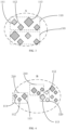
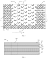
- FIG. 1 illustrates a display panel, including a first display region 100 and a second display region 200; the first display region 100 includes multiple first pixel units 110, and the second display region 200 includes multiple second pixel units 210 and multiple compensation pixel units 300; a pixel density of the first display region 100 is greater than a pixel density of the second display region 200; the first display region 100 and the second display region 200 are connected, and the multiple compensation pixel units 300 are arranged in a region between the second display region 200 and the first display region 100 (a junction of the second display region 200 and the first display region 100); the multiple compensation pixel units 300 are configured to compensate for a color difference between the first display region 100 and the second display region 200.
- Embodiments of the present disclosure provide a display panel including a first display region 100 and a second display region 200; the first display region 100 includes multiple first pixel units 110, each first pixel unit 110 including multiple sub-pixels; the second display region 200 includes multiple second pixel units 210; the pixel density of the first display region is greater than the pixel density of the second display region, which can form a blank region in the second display region 200, and the blank region may be configured to arrange light-transmitting units to realize the light intake of an under-screen camera module, taking into account both the light intake of the under-screen camera module and the display of the second display region 200, which is conducive to realizing the full-screen display of the display panel in a real sense.
- the compensation pixel units 300 at the junction of the first display region 100 and the second display region 200, the problem of color difference between the first display region 100 and the second display region 200 may be solved.
- the display panel provided by the embodiments of the present disclosure will be described in detail as follows.
- the display panel includes a first display region 100 and a second display region 200; the first display region 100 includes multiple first pixel units 110, each first pixel unit 110 including multiple sub-pixels; the second display region 200 includes multiple second pixel units 210, each second pixel unit 210 including multiple sub-pixels; the number of the sub-pixels in each second pixel units 210 is less than the number of the sub-pixels in each first pixel unit 110, and a pixel density of the first display region is greater than a pixel density of the second display region.
- the first display region 100 in the display panel in the embodiments may be a normal display region, and the second display region 200 may be a region facing the under-screen camera.
- the multiple first pixel units 110 are arrayed in the first display region 100, and the multiple second pixel units 210 are arrayed in the second display region 200.
- the first pixel unit 110 may include multiple sub-pixels
- the second pixel unit 210 may include multiple sub-pixels
- the number of sub-pixels in the first pixel unit 110 is greater than the number of sub-pixels in the second pixel unit 210.
- the first pixel unit 110 may include a first sub-pixel 111, two second sub-pixels 112, and a third sub-pixel 113; and the second pixel unit 210 may include a first sub-pixel 111, a second sub-pixel 112, and a third sub-pixel 113.
- the first sub-pixel 111 may be a red sub-pixel (R)
- the second sub-pixel 112 may be a green sub-pixel (G)
- the third sub-pixel 113 may be a blue sub-pixel (B).
- the sub-pixels in the first pixel unit 110 may be arranged in the manner of RGBG and BGRG
- the sub-pixels in the second pixel unit 210 may be arranged in the manner of RGB and BGR.
- the color of the sub-pixels may be other colors in practical applications, and the embodiments of the present disclosure are not limited in this regard.
- the second sub-pixel 112 may be a yellow sub-pixel (Y), in which case the sub-pixels in the first pixel unit 110 may be arranged in the manner of RYBY and BYRY, and the sub-pixels in the second pixel unit 210 may be arranged in the manner of RYB and BYR, etc.
- Y yellow sub-pixel
- the multiple first pixel units 110 are arrayed in the first display region 100, that is, the first display region 100 includes multiple rows of first pixel units 110.
- the first sub-pixel 111 in a first pixel unit 110 in an odd (2n-1, n being a positive integer) row of first pixel units 110 is disposed on a first side of a corresponding third sub-pixel 113
- the first sub-pixel 111 in a first pixel unit 110 in an even (2n, n being a positive integer) rows of first pixel units 110 is disposed on a second side of a corresponding third sub-pixel 113, with the first side opposite to the second side.
- the second sub-pixel 112 is disposed between the corresponding first sub-pixel 111 and the corresponding third sub-pixel 113.
- the red sub-pixel is the first sub-pixel 111
- the green sub-pixel is the second sub-pixel 112
- the blue sub-pixel is the third sub-pixel 113.
- the first pixel units 110 in the first display region 100 in a row near the top of the display panel is the first row of first pixel units.
- the arrangement of the sub-pixels in a first pixel unit 110 in the odd rows may be in the manner of RGBG.
- the red sub-pixel is arranged to the left of the blue sub-pixel, and the centers of the red sub-pixel and the blue sub-pixel are disposed on the same row direction line.
- the centers of the two green sub-pixels are disposed on the same row direction line and are not co-disposed with the centers of the red sub-pixel and the blue sub-pixel, and the two green sub-pixels are disposed on both sides of a column direction center line of the blue sub-pixel.
- the arrangement of the sub-pixels in a first pixel unit 110 in the even rows may be in the manner of BGRG.
- the red sub-pixel is arranged to the right of the blue sub-pixel, and the centers of the red sub-pixel and the blue sub-pixel are disposed on the same row direction line.
- the centers of the two green sub-pixels are disposed on the same row direction line and are not co-disposed with the centers of the red sub-pixel and the blue sub-pixel, and the two green sub-pixels are disposed on both sides of the column direction center line of the blue sub-pixel.
- the row direction is illustrated as an H direction and the column direction is illustrated as an L direction as illustrated in the drawings.
- the second display region 200 may be a rectangular structure, and the first display region 100 includes a first sub-display region 11 and a second sub-display region 12, and the first sub-display region 11 and the second sub-display region 12 are respectively disposed on both sides of the second display region 200 along the row direction.
- Multiple first compensation pixel units 310 are distributed along the column direction between the first sub-display region 11 and the second display region 200
- multiple second compensation pixel units 320 are distributed along the column direction between the second sub-display region 12 and the second display region 200.
- the first compensation pixel units 310 and the second compensation pixel units 320 may solve the problem of color shift and color difference at the junction of the second display region 200 and the first display region 100, which may solve a screen effect of the second display region 200 (under-screen camera region), thereby improving the display quality of the display panel.
- multiple columns of second pixel units 210 are distributed in the second display region 200.
- the first sub-pixel 111 in a second pixel unit 210 in a column near the first sub-display region 11 is closer to the first sub-display region than the third sub-pixel 113 in the same second pixel unit 210.
- the first sub-pixel 111 in a second pixel unit 210 in a column near the second sub-display region 12 is closer to the second sub-display region 12 than the third sub-pixel 113 in the same second pixel unit 210.
- the distribution of the sub-pixel units of each second pixel unit 210 in the multiple second pixel units 210 from the first column to the penultimate column is consistent.
- the first sub-pixel 111 of the same second pixel unit 210 in a column near the first sub-display region 11 is arranged closer to the first sub-display region than the third sub-pixel 113
- the first sub-pixel 111 of the same second pixel unit 210 in a column near the second sub-display region 12 is arranged closer to the second sub-display region 12 than the third sub-pixel 113.
- the second pixel units 210 of the odd (2i-1) columns and the second pixel units 210 of the even (2i) columns are staggered, and further, the second pixel units 210 of the odd (2i-1) columns and the second pixel units 210 of the even (2i) columns are not aligned in the row direction, which may increase the uniformity of the color of the second display region.
- the sub-pixels of the second pixel unit 210 in the column near the first sub-display region 11 may be arranged in an RGB manner.
- the red sub-pixel is the first sub-pixel 111
- the green sub-pixel is the second sub-pixel 112
- the blue sub-pixel is the third sub-pixel 113.
- the red sub-pixel is arranged to the left of the blue sub-pixel, and the centers of the red sub-pixel and the blue sub-pixel are disposed on the same row direction line.
- the green sub-pixel is arranged below a left side of the blue sub-pixel and below a right side of the blue sub-pixel.
- the blue sub-pixel in the second pixel unit 210 in the column near the second sub-display region 12 is arranged on a side of the red sub-pixel unit near the first sub-display region 11, and the green sub-pixel is arranged below a left side of the blue sub-pixel.
- each first compensation pixel unit 310 includes a third sub-pixel 113, which is arranged in the region between the second display region 200 and the first sub-display region 11.
- the number of the compensation pixel units 300 in a column may be the same as the number of second pixel units 210 in one column in the second display region 200.
- the red sub-pixel is the first sub-pixel 111
- the green sub-pixel is the second sub-pixel 112
- the blue sub-pixel is the third sub-pixel 113.
- the first compensation pixel unit 310 may include a blue sub-pixel, which may be disposed in the region between the second display region 200 and the first sub-display region 11.
- the column direction centerline of the blue sub-pixels may coincide with the column direction centerline of the red sub-pixels in the first column of the second pixel units 210, and each blue sub-pixel is arranged below a corresponding red sub-pixel in the first column of the second pixel units 210.
- each second compensation pixel unit 320 includes two second sub-pixels 112 and a third sub-pixel 113.
- the second sub-pixels 112 are disposed on a side of the third sub-pixel 113 away from the first sub-display region 11, and the second compensation pixel units 320 are disposed in the region where the second display region 200 and the second sub-display region 12 meet.
- each second compensation pixel unit 320 may include a blue sub-pixel and two green sub-pixels.
- the blue sub-pixel is arranged on a side of the green sub-pixels away from the second sub-display region 12.
- the column direction centerline of the blue sub-pixels coincides with the column direction centerline of the red sub-pixels in the last column of the second pixel units 210.
- the number of the second compensation pixel units 320 is the same as the number of the second pixel units 210 in one column, and each blue sub-pixel is arranged below a corresponding red sub-pixel.
- one of the two green sub-pixels is disposed to the upper right of the blue sub-pixel, and the row direction center line of the green sub-pixel coincides with the row direction center line of a corresponding green sub-pixel in the last column of second pixel units 210; the other of the two green sub-pixels is disposed to the lower right of the blue sub-pixel, and the row direction center line of the green sub-pixel coincides with the row direction center line of a corresponding green sub-pixel in the last column of second pixel units 210.
- the first compensation pixel units 310 and the second compensation pixel units 320 described above enable the sub-pixels on both sides of the second display region 200 to be arranged in a consistent manner, thereby enabling the color shift and color difference in the second display region to be reduced.
- multiple columns of second pixel units 210 are distributed in the second display region 200.
- the third sub-pixel 113 in a second pixel unit 210 disposed in an odd (2i-1, i being a positive integer) column is disposed on a side of a corresponding first sub-pixel 111 away from the first sub-display region 11, and the third sub-pixel 113 in a second pixel unit 210 disposed in an even (2i, i being a positive integer) column is disposed on a side of a corresponding first sub-pixel 111 near the first sub-display region 11.
- the second pixel units 210 of the odd columns and the second pixel units 210 of the even columns are staggered, i.e., the second pixel units 210 of the odd columns and the second pixel units 210 of the even columns are not aligned in the row direction, to increase the color uniformity.
- the arrangement of the sub-pixels of the second pixel unit 210 in an odd column may be arranged in an RGB manner.
- the red sub-pixel is arranged to the left of the blue sub-pixel, and the centers of the red sub-pixel and the blue sub-pixel are disposed on the same row direction line.
- the green sub-pixel is arranged below a left side of the blue sub-pixel, and the green sub-pixel is arranged below a right side of the blue sub-pixel.
- the red sub-pixel is the first sub-pixel 111
- the green sub-pixel is the second sub-pixel 112
- the blue sub-pixel is the third sub-pixel 113.
- the first compensation pixel unit 310 includes a third sub-pixel 113, which is arranged in the region between the second display region 200 and the first sub-display region 11.
- the number of the compensation pixel units 300 in a column may be the same as the number of second pixel units 210 in one column in the second display region 200.
- the red sub-pixel is the first sub-pixel 111
- the green sub-pixel is the second sub-pixel 112
- the blue sub-pixel is the third sub-pixel 113.
- the first compensation pixel unit 310 may include a blue sub-pixel, which may be disposed in the region between the second display region 200 and the first sub-display region 11.
- the column direction centerline of the blue sub-pixel may coincide with the column direction centerline of the red sub-pixels in the first column of the second pixel units 210, and each blue sub-pixel is arranged below a corresponding red sub-pixel in the first column of the second pixel units 210.
- the second display region 200 includes second pixel units 210 in an even number of columns, and each second compensation pixel unit 320 includes a second sub-pixel 112 and a third sub-pixel 113.
- the second sub-pixel 112 is disposed on a side of the third sub-pixel 113 away from the first sub-display region 11, and the second compensation pixel units 320 are disposed in the region between the second display region 200 and the second sub-display region 12.
- each second compensation pixel unit 320 may include a blue sub-pixel and a green sub-pixel.
- the blue sub-pixel is arranged on a side of the green sub-pixel away from the second sub-display region 12.
- the column direction centerline of the blue sub-pixels coincides with the column direction centerline of the red sub-pixels in the last column of the second pixel units 210.
- the number of the second compensation pixel units 320 is the same as the number of second pixel units 210 in one column, and each blue sub-pixel is arranged below a corresponding red sub-pixel.
- the green sub-pixel is disposed to the upper right of the blue sub-pixel and the row direction centerline of the green sub-pixel coincides with the row direction centerline of a corresponding green sub-pixel in the last column of second pixel units 210.
- a starting column of numbering is the column of second pixel units 210 adjacent to the first sub-display region 11. That is, the first column of second pixel units 210 is adjacent to the first sub-display region 11, and the last column of second pixel units 210 is adjacent to the second sub-display region 12.
- the second display region 200 is arranged with multiple light-transmitting units for transmitting external light to the under-screen camera for imaging.
- the multiple light-transmitting units may be staggered with the second pixel units 210 in the second display region 200.
- the first display region 100 may surround the second display region 200, for example, the second display region 200 may be inside the first display region 100.
- the second display region 200 may be arranged at an edge of the first display region 100, for example, the second display region 200 may be arranged at the top of the first display region 100. In this case, the first display region 100 partially surrounds the second display region 200.
- the pixel arrangement may be a diamond arrangement.
- the first sub-pixel 111 may be a diamond-shaped sub-pixel
- the second sub-pixel 112 may be a diamond-shaped sub-pixel
- the third sub-pixel 113 may be a diamond-shaped sub-pixel.
- the area of the third sub-pixel 113 may be greater than the area of the first sub-pixel 111
- the area of the third sub-pixel 113 may be greater than the area of the second sub-pixel 112.
- the area of the first sub-pixel 111 may be the same as the area of the second sub-pixel 112.
- the first sub-pixel 111, the second sub-pixel 112, and the third sub-pixel 113 may be in other shapes, such as rectangular, triangular, or oval, etc., without limitation herein.
- the pixel density of the first display region is greater than the pixel density of the second display region, for example, the pixel density of the second display region may be one-half of the pixel density of the first display region.
- the ratio of the second pixel density to the second pixel density may be other values in practical applications, and embodiments of the present disclosure are not limited in this regard.
- a display panel provided by embodiments of the present disclosure may be an OLED display panel.
- the display panel may include a substrate 101, a driver circuit layer 102, a pixel electrode layer 103, a light-emitting layer 104, a common electrode layer 105, a pixel definition layer (not shown), and a cover 106, etc.
- the driver circuit layer 102 is arranged on the substrate 101
- the pixel electrode layer 103 is arranged on a side of the driver circuit layer 102 away from the substrate 101
- the light-emitting layer 104 is arranged on a side of the pixel circuit layer 103 away from the driver circuit layer 102.
- the pixel definition layer surrounds a light-emitting unit in the light-emitting layer 104, and the pixel definition layer defines an opening from which the light-emitting unit is exposed.
- the common electrode layer 105 covers the light-emitting unit and the pixel definition layer, and the cover 106 is arranged on a side of the common electrode layer away from the driver circuit layer.
- the light-emitting layer 104 may include a first light-emitting region and a second light-emitting region, the first light-emitting region overlapped with the first pixel region, and the second light-emitting region overlapped with the second pixel region.
- the first light-emitting region may include multiple first light-emitting units
- the second light-emitting region may include multiple second light-emitting units.
- the first light-emitting units are arranged facing the first pixel units 110 in the above embodiments, and the first light-emitting units in the first light-emitting region are distributed in the same manner as the first pixel units 110 in the first display region 100.
- the second light-emitting units are arranged facing the second pixel units 210 in the above embodiments, and the second light-emitting units in the second light-emitting region are distributed in the same manner as the second pixel units 210 in the second display region 200.
- Two sides of the second light-emitting region adjacent to the first light-emitting region may be arranged with first compensation light-emitting units and second compensation light-emitting units, respectively.
- Each first light-emitting unit may include multiple sub-light-emitting units, each sub-light-emitting unit is arranged facing a corresponding sub-pixel in the above embodiments.
- the red sub-pixel corresponds to a red sub-light-emitting unit
- the green sub-pixel corresponds to a green sub-light-emitting unit
- the blue sub-pixel corresponds to a blue sub-light-emitting unit.
- the shape and arrangement of the sub-light-emitting units are consistent with the corresponding sub-pixels.
- the arrangement of sub-light-emitting units in the first light-emitting unit may be in the manner of RGBG or BGRG.
- Each second light-emitting unit may include multiple sub-light-emitting units, and each sub-light-emitting unit is arranged facing a corresponding sub-pixel in the above embodiments.
- the red sub-pixel corresponds to a red sub-light-emitting unit
- the green sub-pixel corresponds to a green sub-light-emitting unit
- the blue sub-pixel corresponds to a blue sub-light-emitting unit.
- the shape and arrangement of the sub-light-emitting units are consistent with the corresponding sub-pixels.
- the arrangement of sub-light-emitting units in the second light-emitting unit may be in the manner of RGB or BGR.
- Each first compensation light-emitting unit may include a blue sub-light-emitting unit
- each second compensation light-emitting unit may include a blue sub-light-emitting unit and a green sub-light-emitting unit.
- the pixel electrode layer 103 includes a first electrode region and a second electrode region, the first electrode region overlapped with the first pixel region, and the second electrode region overlapped with the second pixel region.
- the first electrode region may include multiple first electrode units, and the second electrode region may include multiple second electrode units.
- the first electrode units are arranged facing the first pixel units 110 in the above embodiment, and the first electrode units in the first electrode region are distributed in the same manner as the first pixel units 110 in the first display region 100.
- the second electrode units are arranged facing the second pixel units 210 in the above embodiments, and the second electrode units in the second electrode region are distributed in the same manner as the second pixel units 210 in the second display region 200. Two sides of the second electrode region adjacent to the first electrode region may be arranged with first compensation electrode units and second compensation electrode units, respectively.
- Each first electrode unit may include multiple sub-electrode units, each sub-electrode unit is arranged facing a corresponding sub-pixel in the above embodiments.
- the red sub-pixel corresponds to a red sub-electrode unit
- the green sub-pixel corresponds to a green sub-electrode unit
- the blue sub-pixel corresponds to a blue sub-electrode unit.
- the shape and arrangement of the sub-electrode units are consistent with the corresponding sub-pixels.
- the arrangement of the sub-electrode units in the first electrode unit may be in the manner of RGBG or BGRG.
- Each second electrode unit may include multiple sub-electrode units, and each sub-electrode unit is arranged facing a corresponding sub-pixel in the above embodiments.
- the red sub-pixel corresponds to a red sub-electrode unit
- the green sub-pixel corresponds to a green sub-electrode unit
- the blue sub-pixel corresponds to a blue sub-electrode unit.
- the shape and arrangement of the sub-electrode units are consistent with the corresponding sub-pixels.
- the arrangement of the sub-electrode units in the second electrode unit may be in the manner of RGB or BGR.
- the pixel definition layer includes a first opening region and a second opening region, the first opening region overlapped with the first pixel region, and the second opening region overlapped with the second pixel region. Multiple openings are defined on the first opening region, and each opening is disposed facing a corresponding sub-pixel for exposing a corresponding light-emitting unit.
- the second opening region defines a pixel opening and a light-transmitting opening, the pixel opening facing a corresponding sub-pixel in the second display region 200, and the light-transmitting opening facing a corresponding light-transmitting unit in the second display region 200.
- the pixel openings and the light-transmitting openings are staggered.
- a pixel driving circuit is arranged in the driver circuit layer 102, and the pixel driving circuit includes multiple driving units. Each sub-pixel is connected to a corresponding driving unit, which is configured to provide a drive signal to the sub-pixel.
- the driving unit may be arranged under the sub-pixel, where the light-transmitting unit may not be arranged without a driving unit in a projection region of the driver circuit layer to increase the light transmission of the light-transmitting unit.
- the display panel may be a liquid crystal display panel.
- the display panel may include a substrate 101, a backlight module 107, a driver circuit layer 102, a pixel electrode layer 103, a liquid crystal layer 108, a common electrode layer 105, a color film layer (not shown), a black matrix layer (not shown), and a cover 106, etc.
- the backlight module 107 may be arranged on the substrate 101, the driver circuit layer 102 is arranged on a side of the backlight module 107 away from the substrate 101, the pixel electrode layer 103 is arranged on a side of the driver circuit layer 102 away from the backlight module 107, the liquid crystal layer 108 is arranged on a side of the pixel electrode layer 103 away from the driver circuit layer 102, the common electrode layer 105 is arranged on a side of the liquid crystal layer 108 away from the pixel electrode layer 103, and the color film layer is arranged on a side of the common electrode layer 105 away from the liquid crystal layer.
- the color film layer includes a color pattern, the black matrix layer surrounds the color pattern, and the cover 106 is arranged on a side of the color film layer away from the common electrode layer 105.
- the pixel electrode layer 103 includes a first electrode region and a second electrode region, the first electrode region overlapped with the first pixel region, and the second electrode region overlapped with the second pixel region.
- the first electrode region may include multiple first electrode units, and the second electrode region may include multiple second electrode units.
- the first electrode units are arranged facing the first pixel units 110 in the embodiments, and the first electrode units in the first electrode region are distributed in the same manner as the first pixel units 110 in the first display region 100.
- the second electrode units are arranged facing the second pixel units 210 in the above embodiments, and the second electrode units in the second electrode region are distributed in the same manner as the second pixel units 210 in the second display region 200. Two sides of the second electrode region adj acent to the first electrode region may be arranged with first compensation electrode units and second compensation electrode units, respectively.
- Each first electrode unit may include multiple sub-electrode units, each sub-electrode unit is arranged facing a corresponding sub-pixel in the above embodiments.
- the red sub-pixel corresponds to a red sub-electrode unit
- the green sub-pixel corresponds to a green sub-electrode unit
- the blue sub-pixel corresponds to a blue sub-electrode unit.
- the shape and arrangement of the sub-electrode units are consistent with the corresponding sub-pixels.
- the arrangement of the sub-electrode units in the first electrode unit may be in the manner of RGBG or BGRG.
- Each second electrode unit may include multiple sub-electrode units, and each sub-electrode unit is arranged facing a corresponding sub-pixel in the above embodiments.
- the red sub-pixel corresponds to a red sub-electrode unit
- the green sub-pixel corresponds to a green sub-electrode unit
- the blue sub-pixel corresponds to a blue sub-electrode unit.
- the shape and arrangement of the sub-electrode units are consistent with the corresponding sub-pixels.
- the arrangement of the sub-electrode units in the second electrode unit may be in the manner of RGB or BGR.
- the color film layer is arranged with a color pattern, and the color film layer may include a first pattern region and a second pattern region. Multiple first pattern blocks in multiple colors are arranged in the first pattern region, and the first pattern blocks are arranged facing the first pixel units 110. The arrangement of patterns of the first pattern blocks may be in the manner of RGBG or BGRG, etc. Multiple second pattern blocks in multiple colors are arranged in the second pattern region, and the second pattern block are arranged facing the second pixel units 210. The arrangement of patterns of the second pattern blocks may be in the manner of RGB or BGR, etc. Two sides of the second pattern region adjacent to the first pattern region may be arranged with first compensation patterns and second compensation patterns, respectively.
- the color pattern on the color film layer is exposed to the black matrix layer, i.e., the black matrix layer defines an opening in the region of the color pattern layer.
- the black matrix layer is arranged with a light transmission region in the region facing the second display region 200, which is configured to transmit external light to the under-screen camera.
- the second display region 200 may define a through hole in the projection region of the backlight module to facilitate the passage of light through the backlight module.
- Embodiments of the present disclosure provide a display panel including a first display region 100 and a second display region 200, the first display region 100 including multiple first pixel units 110, the first pixel units 110 including multiple sub-pixels, and the second display region 200 including multiple second pixel units 210; the pixel density of the first display region is greater than the pixel density of the second display region, and the number of sub-pixels in the second pixel unit 210 is less than the number of sub-pixels in the first pixel unit 110.
- the blank region may be formed in the second display region 200, and the blank region may be configured to arrange light-transmitting units to realize the light intake of an under-screen camera module, taking into account both the light intake of the under-screen camera module and the display of the second display region 200, which is conducive to realizing the full-screen display of the display panel in a real sense.
- the compensation pixel units 300 at the junction of the first display region 100 and the second display region 200, the problem of color difference between the first display region 100 and the second display region 200 may be solved.
- the first compensation pixel unit 310 and the second compensation pixel unit 320 can solve the problem of color shift and color difference at the junction of the second display region 200 and the first display region 100, and the first compensation pixel unit 310 and the second compensation pixel unit 320 may enable the sub-pixel arrangement on both sides of the second display region 200 to be consistent, which may solve a screen effect of the second display region 200 (under-screen camera region), thereby improving the display quality of the display panel.
- Embodiments of the present disclosure further provide an electronic device. As illustrated in FIG. 8 , the electronic device includes the display panel 10 described above.
- the electronic device further includes a camera module arranged at a back of the display panel, and the camera module faces the second display region.
- the electronic device may include, for example, a mobile phone, a tablet computer, a television, a laptop computer, a digital photo frame, a navigator, and any other product or component having a display function.
- the electronic device provided by the embodiments of the present disclosure further includes a bezel 20, a main board 30, a battery 40, and a back cover 50.
- the display panel 10 is arranged on the bezel 20 to form a display surface of the electronic device, and the display panel 10 serves as a front housing of the electronic device.
- the back cover 50 is attached to the bezel by double-sided adhesive, and the display panel 10, the bezel 20, and the back cover 50 define a holding space for accommodating other electronic components or functional modules of the electronic device.
- the display panel 10 forms the display surface of the electronic device for displaying images, text, and other information.
- the display panel 10 may be a liquid crystal display or organic light-emitting diode display and other types of displays.
- the display panel 10 may be arranged with a glass cover.
- the glass cover may cover the display panel 10 to protect the display panel 10 from being scratched or damaged by water.
- the display panel 10 may be a full-screen display panel. In this case, the display panel 10 can display information in full screen, such that the electronic device has a large screen-to-body ratio.
- the display panel 10 may have a first display region 100 and a second display region 200.
- An under-screen camera requires the display screen to be translucent when in use. Therefore, arranging a light-transmitting region in the second display region of low pixel density can increase the light transmission rate.
- the camera module 410 may be a front camera. Functional modules such as a proximity sensor may be hidden under the display panel 10, while a fingerprint recognition module of the electronic device may be arranged on the back of the electronic device.
- the bezel 20 may be a hollow frame structure.
- the material of the bezel 20 may include metal or plastic.
- the main board 30 is arranged inside the holding space.
- the main board 30 may be arranged on the bezel 20 and accommodated in the holding space along with the bezel 20.
- the main board 30 is arranged with a grounding point to achieve grounding of the main board 30.
- the main board 30 may have one or more of a motor, a microphone, a speaker, a receiver, a headphone interface, a universal serial bus interface (USB interface), a camera, a proximity sensor, an ambient light sensor, a gyroscope, and a processor and other functional modules integrated on the main board 30.
- the display panel 10 may be electrically connected to the main board 30.
- the main board 30 is arranged with a display control circuit.
- the display control circuit outputs electrical signals to the display panel 10 to control the display panel 10 to display information.
- the battery 40 is arranged inside the holding space.
- the battery 40 may be arranged on the bezel 20 and accommodated in the holding space along with the bezel 20.
- the battery 40 may be electrically connected to the main board 30 to enable the battery 40 to power the electronic device.
- the main board 30 may be arranged with a power management circuit.
- the power management circuit is configured to distribute voltage provided by the battery 40 to various electronic components in the electronic device.
- the back cover 50 is configured to form an external contour of the electronic device.
- the back cover 50 may be molded in one piece. During the molding of the back cover 50, structures such as a rear camera hole, a fingerprint recognition module mounting hole, etc. may be defined on the back cover 50.
Landscapes
- Engineering & Computer Science (AREA)
- Physics & Mathematics (AREA)
- Computer Hardware Design (AREA)
- General Physics & Mathematics (AREA)
- Theoretical Computer Science (AREA)
- Chemical & Material Sciences (AREA)
- Crystallography & Structural Chemistry (AREA)
- Devices For Indicating Variable Information By Combining Individual Elements (AREA)
- Electroluminescent Light Sources (AREA)
Abstract
Description
- The present disclosure claims priority of
Chinese Patent Application No. 202010905906.3, in the title of "DISPLAY PANEL AND ELECTRONIC DEVICE", filed on September 01, 2020 - The present disclosure relates to the field of electronic device technologies, and in particular to a display panel, a display apparatus, and an electronic device.
- With the development and progress of technology, full-screen is increasingly and widely used in various terminal devices, but for terminal devices with front cameras, the need to consider the installation of front cameras makes it difficult to achieve full-screen in the real sense of the current mobile phones or other mobile terminal devices. Therefore, how to truly realize the coexistence of full-screen and front camera is a problem that is required to be solved.
- It should be noted that the information disclosed in the Background section is only for the purpose of enhancing the understanding of the background of the present disclosure, and thus may include information that does not constitute prior art known to those skilled in the art.
- The purpose of the present disclosure is to provide a display panel, a display apparatus, and an electronic device, thereby solving, at least in part, one or more problems caused by defects in the related art.
- According to a first aspect, the present disclosure provides a display panel, including:
- a first display region, including a plurality of first pixel units; and
- a second display region, including a plurality of second pixel units and a plurality of compensation pixel units; wherein a pixel density of the first display region is greater than a pixel density of the second display region; the first display region and the second display region are connected, and the plurality of compensation pixel units are arranged in a region between the second display region and the first display region; the plurality of compensation pixel units are configured to compensate for a color difference between the first display region and the second display region.
- According to a second aspect, the present disclosure provides a display apparatus, including:
- the display panel as above; and
- a transparent cover, arranged on a light-emitting side of the display panel.
- According to a third aspect, the present disclosure provides an electronic device, including the display apparatus as above.
- It can be understood that the above general description and the later detailed descriptions are exemplary and explanatory only and do not limit the present disclosure.
- The accompanying drawings herein are incorporated into and form part of the specification, illustrate embodiments consistent with the present disclosure, and are used in conjunction with the specification to explain the principles of the present disclosure. It will be apparent that the accompanying drawings in the following description are only some embodiments of the present disclosure, and that other drawings may be obtained from them without creative effort by those skilled in the art.
-
FIG. 1 is a schematic view of pixel distribution of a display panel according to an embodiment of the present disclosure. -
FIG. 2 is a schematic view of pixel distribution of a display panel according to another embodiment of the present disclosure. -
FIG. 3 is a partial enlarged view of area A circumscribed inFIG. 2 . -
FIG. 4 is a partial enlarged view of area B circumscribed inFIG. 2 . -
FIG. 5 is a schematic view of pixel distribution of a display panel according to further another embodiment of the present disclosure. -
FIG. 6 is a schematic view of a display panel according to an embodiment of the present disclosure. -
FIG. 7 is a schematic view of a display panel according to another embodiment of the present disclosure. -
FIG. 8 is a schematic view of an electronic device according to an embodiment of the present disclosure. - Embodiments will now be described more fully with reference to the accompanying drawings. However, the embodiments may be implemented in a variety of forms and should not be construed as being limited to the embodiments set forth herein; rather, the provision of these embodiments allows the present disclosure to be comprehensive and complete and communicates the ideas of the embodiments in a comprehensive manner to those skilled in the art. Identical reference signs in the drawings indicate identical or similar structures, and thus their detailed description will be omitted.
- Although relative terms such as "up" and "down" are used in this specification to describe a relative relationship of one component to another, these terms are used in this specification only for convenience, for example, according to the orientation of the embodiments described in the accompanying drawings. It is understood that when a device is flipped such that it is upside down, the component described as being "up" will become the component described as being "down". When a structure is "on" other structures, it may mean that the structure is integrally formed on other structures, or that the structure is "directly" arranged on other structures, or that the structure is "indirectly" arranged on other structures through another structure.
- Embodiments of the present disclosure first provide a display panel.
FIG. 1 illustrates a display panel, including afirst display region 100 and asecond display region 200; thefirst display region 100 includes multiplefirst pixel units 110, and thesecond display region 200 includes multiplesecond pixel units 210 and multiplecompensation pixel units 300; a pixel density of thefirst display region 100 is greater than a pixel density of thesecond display region 200; thefirst display region 100 and thesecond display region 200 are connected, and the multiplecompensation pixel units 300 are arranged in a region between thesecond display region 200 and the first display region 100 (a junction of thesecond display region 200 and the first display region 100); the multiplecompensation pixel units 300 are configured to compensate for a color difference between thefirst display region 100 and thesecond display region 200. - Embodiments of the present disclosure provide a display panel including a
first display region 100 and asecond display region 200; thefirst display region 100 includes multiplefirst pixel units 110, eachfirst pixel unit 110 including multiple sub-pixels; thesecond display region 200 includes multiplesecond pixel units 210; the pixel density of the first display region is greater than the pixel density of the second display region, which can form a blank region in thesecond display region 200, and the blank region may be configured to arrange light-transmitting units to realize the light intake of an under-screen camera module, taking into account both the light intake of the under-screen camera module and the display of thesecond display region 200, which is conducive to realizing the full-screen display of the display panel in a real sense. In addition, by arranging thecompensation pixel units 300 at the junction of thefirst display region 100 and thesecond display region 200, the problem of color difference between thefirst display region 100 and thesecond display region 200 may be solved. - The display panel provided by the embodiments of the present disclosure will be described in detail as follows.
- The display panel includes a
first display region 100 and asecond display region 200; thefirst display region 100 includes multiplefirst pixel units 110, eachfirst pixel unit 110 including multiple sub-pixels; thesecond display region 200 includes multiplesecond pixel units 210, eachsecond pixel unit 210 including multiple sub-pixels; the number of the sub-pixels in eachsecond pixel units 210 is less than the number of the sub-pixels in eachfirst pixel unit 110, and a pixel density of the first display region is greater than a pixel density of the second display region. - The
first display region 100 in the display panel in the embodiments may be a normal display region, and thesecond display region 200 may be a region facing the under-screen camera. The multiplefirst pixel units 110 are arrayed in thefirst display region 100, and the multiplesecond pixel units 210 are arrayed in thesecond display region 200. - The
first pixel unit 110 may include multiple sub-pixels, and thesecond pixel unit 210 may include multiple sub-pixels, and the number of sub-pixels in thefirst pixel unit 110 is greater than the number of sub-pixels in thesecond pixel unit 210. - Exemplarily, as illustrated in
FIG. 2 , thefirst pixel unit 110 may include afirst sub-pixel 111, twosecond sub-pixels 112, and athird sub-pixel 113; and thesecond pixel unit 210 may include afirst sub-pixel 111, asecond sub-pixel 112, and athird sub-pixel 113. - The
first sub-pixel 111 may be a red sub-pixel (R), thesecond sub-pixel 112 may be a green sub-pixel (G), and thethird sub-pixel 113 may be a blue sub-pixel (B). As illustrated inFIG. 3 , the sub-pixels in thefirst pixel unit 110 may be arranged in the manner of RGBG and BGRG, and the sub-pixels in thesecond pixel unit 210 may be arranged in the manner of RGB and BGR. Of course, the color of the sub-pixels may be other colors in practical applications, and the embodiments of the present disclosure are not limited in this regard. For example, thesecond sub-pixel 112 may be a yellow sub-pixel (Y), in which case the sub-pixels in thefirst pixel unit 110 may be arranged in the manner of RYBY and BYRY, and the sub-pixels in thesecond pixel unit 210 may be arranged in the manner of RYB and BYR, etc. - The multiple
first pixel units 110 are arrayed in thefirst display region 100, that is, thefirst display region 100 includes multiple rows offirst pixel units 110. Thefirst sub-pixel 111 in afirst pixel unit 110 in an odd (2n-1, n being a positive integer) row offirst pixel units 110 is disposed on a first side of a correspondingthird sub-pixel 113, and thefirst sub-pixel 111 in afirst pixel unit 110 in an even (2n, n being a positive integer) rows offirst pixel units 110 is disposed on a second side of a correspondingthird sub-pixel 113, with the first side opposite to the second side. Thesecond sub-pixel 112 is disposed between the correspondingfirst sub-pixel 111 and the correspondingthird sub-pixel 113. - Exemplarily, the red sub-pixel is the
first sub-pixel 111, the green sub-pixel is thesecond sub-pixel 112, and the blue sub-pixel is thethird sub-pixel 113. Thefirst pixel units 110 in thefirst display region 100 in a row near the top of the display panel is the first row of first pixel units. The arrangement of the sub-pixels in afirst pixel unit 110 in the odd rows may be in the manner of RGBG. The red sub-pixel is arranged to the left of the blue sub-pixel, and the centers of the red sub-pixel and the blue sub-pixel are disposed on the same row direction line. The centers of the two green sub-pixels are disposed on the same row direction line and are not co-disposed with the centers of the red sub-pixel and the blue sub-pixel, and the two green sub-pixels are disposed on both sides of a column direction center line of the blue sub-pixel. - The arrangement of the sub-pixels in a
first pixel unit 110 in the even rows may be in the manner of BGRG. The red sub-pixel is arranged to the right of the blue sub-pixel, and the centers of the red sub-pixel and the blue sub-pixel are disposed on the same row direction line. The centers of the two green sub-pixels are disposed on the same row direction line and are not co-disposed with the centers of the red sub-pixel and the blue sub-pixel, and the two green sub-pixels are disposed on both sides of the column direction center line of the blue sub-pixel. Among them, in the embodiments, the row direction is illustrated as an H direction and the column direction is illustrated as an L direction as illustrated in the drawings. - The
second display region 200 may be a rectangular structure, and thefirst display region 100 includes a firstsub-display region 11 and a secondsub-display region 12, and the firstsub-display region 11 and thesecond sub-display region 12 are respectively disposed on both sides of thesecond display region 200 along the row direction. Multiple firstcompensation pixel units 310 are distributed along the column direction between the firstsub-display region 11 and thesecond display region 200, and multiple secondcompensation pixel units 320 are distributed along the column direction between thesecond sub-display region 12 and thesecond display region 200. - The first
compensation pixel units 310 and the secondcompensation pixel units 320 may solve the problem of color shift and color difference at the junction of thesecond display region 200 and thefirst display region 100, which may solve a screen effect of the second display region 200 (under-screen camera region), thereby improving the display quality of the display panel. - In some embodiments of the present disclosure, as illustrated in
FIG. 2 , multiple columns ofsecond pixel units 210 are distributed in thesecond display region 200. Thefirst sub-pixel 111 in asecond pixel unit 210 in a column near the firstsub-display region 11 is closer to the first sub-display region than thethird sub-pixel 113 in the samesecond pixel unit 210. Thefirst sub-pixel 111 in asecond pixel unit 210 in a column near thesecond sub-display region 12 is closer to thesecond sub-display region 12 than thethird sub-pixel 113 in the samesecond pixel unit 210. - By starting a column count in the direction from the first
sub-display region 10 to thesecond sub-display region 20, the distribution of the sub-pixel units of eachsecond pixel unit 210 in the multiplesecond pixel units 210 from the first column to the penultimate column is consistent. - The
first sub-pixel 111 of the samesecond pixel unit 210 in a column near the firstsub-display region 11 is arranged closer to the first sub-display region than thethird sub-pixel 113, and thefirst sub-pixel 111 of the samesecond pixel unit 210 in a column near thesecond sub-display region 12 is arranged closer to thesecond sub-display region 12 than thethird sub-pixel 113. Thesecond pixel units 210 of the odd (2i-1) columns and thesecond pixel units 210 of the even (2i) columns are staggered, and further, thesecond pixel units 210 of the odd (2i-1) columns and thesecond pixel units 210 of the even (2i) columns are not aligned in the row direction, which may increase the uniformity of the color of the second display region. - Exemplarily, the sub-pixels of the
second pixel unit 210 in the column near the firstsub-display region 11 may be arranged in an RGB manner. The red sub-pixel is thefirst sub-pixel 111, the green sub-pixel is thesecond sub-pixel 112, and the blue sub-pixel is thethird sub-pixel 113. The red sub-pixel is arranged to the left of the blue sub-pixel, and the centers of the red sub-pixel and the blue sub-pixel are disposed on the same row direction line. The green sub-pixel is arranged below a left side of the blue sub-pixel and below a right side of the blue sub-pixel. The blue sub-pixel in thesecond pixel unit 210 in the column near thesecond sub-display region 12 is arranged on a side of the red sub-pixel unit near the firstsub-display region 11, and the green sub-pixel is arranged below a left side of the blue sub-pixel. - On this basis, each first
compensation pixel unit 310 includes athird sub-pixel 113, which is arranged in the region between thesecond display region 200 and the firstsub-display region 11. The number of thecompensation pixel units 300 in a column may be the same as the number ofsecond pixel units 210 in one column in thesecond display region 200. - Exemplarily, the red sub-pixel is the
first sub-pixel 111, the green sub-pixel is thesecond sub-pixel 112, and the blue sub-pixel is thethird sub-pixel 113. The firstcompensation pixel unit 310 may include a blue sub-pixel, which may be disposed in the region between thesecond display region 200 and the firstsub-display region 11. The column direction centerline of the blue sub-pixels may coincide with the column direction centerline of the red sub-pixels in the first column of thesecond pixel units 210, and each blue sub-pixel is arranged below a corresponding red sub-pixel in the first column of thesecond pixel units 210. - As illustrated in
FIG. 4 , each secondcompensation pixel unit 320 includes twosecond sub-pixels 112 and athird sub-pixel 113. In the same secondcompensation pixel unit 320, the second sub-pixels 112 are disposed on a side of thethird sub-pixel 113 away from the firstsub-display region 11, and the secondcompensation pixel units 320 are disposed in the region where thesecond display region 200 and thesecond sub-display region 12 meet. - Exemplarily, the red sub-pixel is the
first sub-pixel 111, the green sub-pixel is thesecond sub-pixel 112, and the blue sub-pixel is thethird sub-pixel 113. Each secondcompensation pixel unit 320 may include a blue sub-pixel and two green sub-pixels. The blue sub-pixel is arranged on a side of the green sub-pixels away from thesecond sub-display region 12. The column direction centerline of the blue sub-pixels coincides with the column direction centerline of the red sub-pixels in the last column of thesecond pixel units 210. The number of the secondcompensation pixel units 320 is the same as the number of thesecond pixel units 210 in one column, and each blue sub-pixel is arranged below a corresponding red sub-pixel. one of the two green sub-pixels is disposed to the upper right of the blue sub-pixel, and the row direction center line of the green sub-pixel coincides with the row direction center line of a corresponding green sub-pixel in the last column ofsecond pixel units 210; the other of the two green sub-pixels is disposed to the lower right of the blue sub-pixel, and the row direction center line of the green sub-pixel coincides with the row direction center line of a corresponding green sub-pixel in the last column ofsecond pixel units 210. - The first
compensation pixel units 310 and the secondcompensation pixel units 320 described above enable the sub-pixels on both sides of thesecond display region 200 to be arranged in a consistent manner, thereby enabling the color shift and color difference in the second display region to be reduced. - In others embodiment of the present disclosure, as illustrated in
FIG. 5 , multiple columns ofsecond pixel units 210 are distributed in thesecond display region 200. Thethird sub-pixel 113 in asecond pixel unit 210 disposed in an odd (2i-1, i being a positive integer) column is disposed on a side of a correspondingfirst sub-pixel 111 away from the firstsub-display region 11, and thethird sub-pixel 113 in asecond pixel unit 210 disposed in an even (2i, i being a positive integer) column is disposed on a side of a correspondingfirst sub-pixel 111 near the firstsub-display region 11. Thesecond pixel units 210 of the odd columns and thesecond pixel units 210 of the even columns are staggered, i.e., thesecond pixel units 210 of the odd columns and thesecond pixel units 210 of the even columns are not aligned in the row direction, to increase the color uniformity. - Exemplarily, the arrangement of the sub-pixels of the
second pixel unit 210 in an odd column may be arranged in an RGB manner. The red sub-pixel is arranged to the left of the blue sub-pixel, and the centers of the red sub-pixel and the blue sub-pixel are disposed on the same row direction line. The green sub-pixel is arranged below a left side of the blue sub-pixel, and the green sub-pixel is arranged below a right side of the blue sub-pixel. The red sub-pixel is thefirst sub-pixel 111, the green sub-pixel is thesecond sub-pixel 112, and the blue sub-pixel is thethird sub-pixel 113. - On this basis, the first
compensation pixel unit 310 includes athird sub-pixel 113, which is arranged in the region between thesecond display region 200 and the firstsub-display region 11. The number of thecompensation pixel units 300 in a column may be the same as the number ofsecond pixel units 210 in one column in thesecond display region 200. - Exemplarily, the red sub-pixel is the
first sub-pixel 111, the green sub-pixel is thesecond sub-pixel 112, and the blue sub-pixel is thethird sub-pixel 113. The firstcompensation pixel unit 310 may include a blue sub-pixel, which may be disposed in the region between thesecond display region 200 and the firstsub-display region 11. The column direction centerline of the blue sub-pixel may coincide with the column direction centerline of the red sub-pixels in the first column of thesecond pixel units 210, and each blue sub-pixel is arranged below a corresponding red sub-pixel in the first column of thesecond pixel units 210. - The
second display region 200 includessecond pixel units 210 in an even number of columns, and each secondcompensation pixel unit 320 includes asecond sub-pixel 112 and athird sub-pixel 113. In the secondcompensation pixel unit 320, thesecond sub-pixel 112 is disposed on a side of thethird sub-pixel 113 away from the firstsub-display region 11, and the secondcompensation pixel units 320 are disposed in the region between thesecond display region 200 and thesecond sub-display region 12. - Exemplarily, the red sub-pixel is the
first sub-pixel 111, the green sub-pixel is thesecond sub-pixel 112, and the blue sub-pixel is thethird sub-pixel 113. Each secondcompensation pixel unit 320 may include a blue sub-pixel and a green sub-pixel. The blue sub-pixel is arranged on a side of the green sub-pixel away from thesecond sub-display region 12. The column direction centerline of the blue sub-pixels coincides with the column direction centerline of the red sub-pixels in the last column of thesecond pixel units 210. The number of the secondcompensation pixel units 320 is the same as the number ofsecond pixel units 210 in one column, and each blue sub-pixel is arranged below a corresponding red sub-pixel. The green sub-pixel is disposed to the upper right of the blue sub-pixel and the row direction centerline of the green sub-pixel coincides with the row direction centerline of a corresponding green sub-pixel in the last column ofsecond pixel units 210. - It should be noted that among the multiple columns of
second pixel units 210 in thesecond display region 200 in the embodiments, a starting column of numbering is the column ofsecond pixel units 210 adjacent to the firstsub-display region 11. That is, the first column ofsecond pixel units 210 is adjacent to the firstsub-display region 11, and the last column ofsecond pixel units 210 is adjacent to thesecond sub-display region 12. - When the display panel is applied to an electronic device with an under-screen camera, the
second display region 200 is arranged with multiple light-transmitting units for transmitting external light to the under-screen camera for imaging. The multiple light-transmitting units may be staggered with thesecond pixel units 210 in thesecond display region 200. - The
first display region 100 may surround thesecond display region 200, for example, thesecond display region 200 may be inside thefirst display region 100. Alternatively, thesecond display region 200 may be arranged at an edge of thefirst display region 100, for example, thesecond display region 200 may be arranged at the top of thefirst display region 100. In this case, thefirst display region 100 partially surrounds thesecond display region 200. - In some embodiments, the pixel arrangement may be a diamond arrangement. The
first sub-pixel 111 may be a diamond-shaped sub-pixel, thesecond sub-pixel 112 may be a diamond-shaped sub-pixel, and thethird sub-pixel 113 may be a diamond-shaped sub-pixel. The area of thethird sub-pixel 113 may be greater than the area of thefirst sub-pixel 111, and the area of thethird sub-pixel 113 may be greater than the area of thesecond sub-pixel 112. The area of thefirst sub-pixel 111 may be the same as the area of thesecond sub-pixel 112. Of course, in practical applications, thefirst sub-pixel 111, thesecond sub-pixel 112, and thethird sub-pixel 113 may be in other shapes, such as rectangular, triangular, or oval, etc., without limitation herein. - The pixel density of the first display region is greater than the pixel density of the second display region, for example, the pixel density of the second display region may be one-half of the pixel density of the first display region. Of course, the ratio of the second pixel density to the second pixel density may be other values in practical applications, and embodiments of the present disclosure are not limited in this regard.
- A display panel provided by embodiments of the present disclosure may be an OLED display panel. As illustrated in
FIG. 6 , the display panel may include asubstrate 101, adriver circuit layer 102, apixel electrode layer 103, a light-emittinglayer 104, acommon electrode layer 105, a pixel definition layer (not shown), and acover 106, etc. Thedriver circuit layer 102 is arranged on thesubstrate 101, thepixel electrode layer 103 is arranged on a side of thedriver circuit layer 102 away from thesubstrate 101, and the light-emittinglayer 104 is arranged on a side of thepixel circuit layer 103 away from thedriver circuit layer 102. The pixel definition layer surrounds a light-emitting unit in the light-emittinglayer 104, and the pixel definition layer defines an opening from which the light-emitting unit is exposed. Thecommon electrode layer 105 covers the light-emitting unit and the pixel definition layer, and thecover 106 is arranged on a side of the common electrode layer away from the driver circuit layer. - The light-emitting
layer 104 may include a first light-emitting region and a second light-emitting region, the first light-emitting region overlapped with the first pixel region, and the second light-emitting region overlapped with the second pixel region. The first light-emitting region may include multiple first light-emitting units, and the second light-emitting region may include multiple second light-emitting units. The first light-emitting units are arranged facing thefirst pixel units 110 in the above embodiments, and the first light-emitting units in the first light-emitting region are distributed in the same manner as thefirst pixel units 110 in thefirst display region 100. The second light-emitting units are arranged facing thesecond pixel units 210 in the above embodiments, and the second light-emitting units in the second light-emitting region are distributed in the same manner as thesecond pixel units 210 in thesecond display region 200. Two sides of the second light-emitting region adjacent to the first light-emitting region may be arranged with first compensation light-emitting units and second compensation light-emitting units, respectively. - Each first light-emitting unit may include multiple sub-light-emitting units, each sub-light-emitting unit is arranged facing a corresponding sub-pixel in the above embodiments. The red sub-pixel corresponds to a red sub-light-emitting unit, the green sub-pixel corresponds to a green sub-light-emitting unit, and the blue sub-pixel corresponds to a blue sub-light-emitting unit. The shape and arrangement of the sub-light-emitting units are consistent with the corresponding sub-pixels. For example, the arrangement of sub-light-emitting units in the first light-emitting unit may be in the manner of RGBG or BGRG.
- Each second light-emitting unit may include multiple sub-light-emitting units, and each sub-light-emitting unit is arranged facing a corresponding sub-pixel in the above embodiments. The red sub-pixel corresponds to a red sub-light-emitting unit, the green sub-pixel corresponds to a green sub-light-emitting unit, and the blue sub-pixel corresponds to a blue sub-light-emitting unit. The shape and arrangement of the sub-light-emitting units are consistent with the corresponding sub-pixels. For example, the arrangement of sub-light-emitting units in the second light-emitting unit may be in the manner of RGB or BGR. Each first compensation light-emitting unit may include a blue sub-light-emitting unit, and each second compensation light-emitting unit may include a blue sub-light-emitting unit and a green sub-light-emitting unit.
- The
pixel electrode layer 103 includes a first electrode region and a second electrode region, the first electrode region overlapped with the first pixel region, and the second electrode region overlapped with the second pixel region. The first electrode region may include multiple first electrode units, and the second electrode region may include multiple second electrode units. The first electrode units are arranged facing thefirst pixel units 110 in the above embodiment, and the first electrode units in the first electrode region are distributed in the same manner as thefirst pixel units 110 in thefirst display region 100. The second electrode units are arranged facing thesecond pixel units 210 in the above embodiments, and the second electrode units in the second electrode region are distributed in the same manner as thesecond pixel units 210 in thesecond display region 200. Two sides of the second electrode region adjacent to the first electrode region may be arranged with first compensation electrode units and second compensation electrode units, respectively. - Each first electrode unit may include multiple sub-electrode units, each sub-electrode unit is arranged facing a corresponding sub-pixel in the above embodiments. The red sub-pixel corresponds to a red sub-electrode unit, the green sub-pixel corresponds to a green sub-electrode unit, and the blue sub-pixel corresponds to a blue sub-electrode unit. The shape and arrangement of the sub-electrode units are consistent with the corresponding sub-pixels. For example, the arrangement of the sub-electrode units in the first electrode unit may be in the manner of RGBG or BGRG.
- Each second electrode unit may include multiple sub-electrode units, and each sub-electrode unit is arranged facing a corresponding sub-pixel in the above embodiments. The red sub-pixel corresponds to a red sub-electrode unit, the green sub-pixel corresponds to a green sub-electrode unit, and the blue sub-pixel corresponds to a blue sub-electrode unit. The shape and arrangement of the sub-electrode units are consistent with the corresponding sub-pixels. For example, the arrangement of the sub-electrode units in the second electrode unit may be in the manner of RGB or BGR.
- The pixel definition layer includes a first opening region and a second opening region, the first opening region overlapped with the first pixel region, and the second opening region overlapped with the second pixel region. Multiple openings are defined on the first opening region, and each opening is disposed facing a corresponding sub-pixel for exposing a corresponding light-emitting unit. The second opening region defines a pixel opening and a light-transmitting opening, the pixel opening facing a corresponding sub-pixel in the
second display region 200, and the light-transmitting opening facing a corresponding light-transmitting unit in thesecond display region 200. The pixel openings and the light-transmitting openings are staggered. - A pixel driving circuit is arranged in the
driver circuit layer 102, and the pixel driving circuit includes multiple driving units. Each sub-pixel is connected to a corresponding driving unit, which is configured to provide a drive signal to the sub-pixel. The driving unit may be arranged under the sub-pixel, where the light-transmitting unit may not be arranged without a driving unit in a projection region of the driver circuit layer to increase the light transmission of the light-transmitting unit. - It is understood that the display panel may be a liquid crystal display panel. As illustrated in
FIG. 7 , the display panel may include asubstrate 101, abacklight module 107, adriver circuit layer 102, apixel electrode layer 103, aliquid crystal layer 108, acommon electrode layer 105, a color film layer (not shown), a black matrix layer (not shown), and acover 106, etc. Thebacklight module 107 may be arranged on thesubstrate 101, thedriver circuit layer 102 is arranged on a side of thebacklight module 107 away from thesubstrate 101, thepixel electrode layer 103 is arranged on a side of thedriver circuit layer 102 away from thebacklight module 107, theliquid crystal layer 108 is arranged on a side of thepixel electrode layer 103 away from thedriver circuit layer 102, thecommon electrode layer 105 is arranged on a side of theliquid crystal layer 108 away from thepixel electrode layer 103, and the color film layer is arranged on a side of thecommon electrode layer 105 away from the liquid crystal layer. The color film layer includes a color pattern, the black matrix layer surrounds the color pattern, and thecover 106 is arranged on a side of the color film layer away from thecommon electrode layer 105. - The
pixel electrode layer 103 includes a first electrode region and a second electrode region, the first electrode region overlapped with the first pixel region, and the second electrode region overlapped with the second pixel region. The first electrode region may include multiple first electrode units, and the second electrode region may include multiple second electrode units. The first electrode units are arranged facing thefirst pixel units 110 in the embodiments, and the first electrode units in the first electrode region are distributed in the same manner as thefirst pixel units 110 in thefirst display region 100. The second electrode units are arranged facing thesecond pixel units 210 in the above embodiments, and the second electrode units in the second electrode region are distributed in the same manner as thesecond pixel units 210 in thesecond display region 200. Two sides of the second electrode region adj acent to the first electrode region may be arranged with first compensation electrode units and second compensation electrode units, respectively. - Each first electrode unit may include multiple sub-electrode units, each sub-electrode unit is arranged facing a corresponding sub-pixel in the above embodiments. The red sub-pixel corresponds to a red sub-electrode unit, the green sub-pixel corresponds to a green sub-electrode unit, and the blue sub-pixel corresponds to a blue sub-electrode unit. The shape and arrangement of the sub-electrode units are consistent with the corresponding sub-pixels. For example, the arrangement of the sub-electrode units in the first electrode unit may be in the manner of RGBG or BGRG.
- Each second electrode unit may include multiple sub-electrode units, and each sub-electrode unit is arranged facing a corresponding sub-pixel in the above embodiments. The red sub-pixel corresponds to a red sub-electrode unit, the green sub-pixel corresponds to a green sub-electrode unit, and the blue sub-pixel corresponds to a blue sub-electrode unit. The shape and arrangement of the sub-electrode units are consistent with the corresponding sub-pixels. For example, the arrangement of the sub-electrode units in the second electrode unit may be in the manner of RGB or BGR.
- The color film layer is arranged with a color pattern, and the color film layer may include a first pattern region and a second pattern region. Multiple first pattern blocks in multiple colors are arranged in the first pattern region, and the first pattern blocks are arranged facing the
first pixel units 110. The arrangement of patterns of the first pattern blocks may be in the manner of RGBG or BGRG, etc. Multiple second pattern blocks in multiple colors are arranged in the second pattern region, and the second pattern block are arranged facing thesecond pixel units 210. The arrangement of patterns of the second pattern blocks may be in the manner of RGB or BGR, etc. Two sides of the second pattern region adjacent to the first pattern region may be arranged with first compensation patterns and second compensation patterns, respectively. - The color pattern on the color film layer is exposed to the black matrix layer, i.e., the black matrix layer defines an opening in the region of the color pattern layer. The black matrix layer is arranged with a light transmission region in the region facing the
second display region 200, which is configured to transmit external light to the under-screen camera. Thesecond display region 200 may define a through hole in the projection region of the backlight module to facilitate the passage of light through the backlight module. - Embodiments of the present disclosure provide a display panel including a
first display region 100 and asecond display region 200, thefirst display region 100 including multiplefirst pixel units 110, thefirst pixel units 110 including multiple sub-pixels, and thesecond display region 200 including multiplesecond pixel units 210; the pixel density of the first display region is greater than the pixel density of the second display region, and the number of sub-pixels in thesecond pixel unit 210 is less than the number of sub-pixels in thefirst pixel unit 110. The blank region may be formed in thesecond display region 200, and the blank region may be configured to arrange light-transmitting units to realize the light intake of an under-screen camera module, taking into account both the light intake of the under-screen camera module and the display of thesecond display region 200, which is conducive to realizing the full-screen display of the display panel in a real sense. In addition, by arranging thecompensation pixel units 300 at the junction of thefirst display region 100 and thesecond display region 200, the problem of color difference between thefirst display region 100 and thesecond display region 200 may be solved. - The first
compensation pixel unit 310 and the secondcompensation pixel unit 320 can solve the problem of color shift and color difference at the junction of thesecond display region 200 and thefirst display region 100, and the firstcompensation pixel unit 310 and the secondcompensation pixel unit 320 may enable the sub-pixel arrangement on both sides of thesecond display region 200 to be consistent, which may solve a screen effect of the second display region 200 (under-screen camera region), thereby improving the display quality of the display panel. - Embodiments of the present disclosure further provide an electronic device. As illustrated in
FIG. 8 , the electronic device includes thedisplay panel 10 described above. - Further, the electronic device further includes a camera module arranged at a back of the display panel, and the camera module faces the second display region.
- The electronic device may include, for example, a mobile phone, a tablet computer, a television, a laptop computer, a digital photo frame, a navigator, and any other product or component having a display function.
- As illustrated in
FIG. 8 , the electronic device provided by the embodiments of the present disclosure further includes abezel 20, amain board 30, abattery 40, and aback cover 50. Thedisplay panel 10 is arranged on thebezel 20 to form a display surface of the electronic device, and thedisplay panel 10 serves as a front housing of the electronic device. Theback cover 50 is attached to the bezel by double-sided adhesive, and thedisplay panel 10, thebezel 20, and theback cover 50 define a holding space for accommodating other electronic components or functional modules of the electronic device. In addition, thedisplay panel 10 forms the display surface of the electronic device for displaying images, text, and other information. Thedisplay panel 10 may be a liquid crystal display or organic light-emitting diode display and other types of displays. - The
display panel 10 may be arranged with a glass cover. The glass cover may cover thedisplay panel 10 to protect thedisplay panel 10 from being scratched or damaged by water. - The
display panel 10 may be a full-screen display panel. In this case, thedisplay panel 10 can display information in full screen, such that the electronic device has a large screen-to-body ratio. Thedisplay panel 10 may have afirst display region 100 and asecond display region 200. An under-screen camera requires the display screen to be translucent when in use. Therefore, arranging a light-transmitting region in the second display region of low pixel density can increase the light transmission rate. Thecamera module 410 may be a front camera. Functional modules such as a proximity sensor may be hidden under thedisplay panel 10, while a fingerprint recognition module of the electronic device may be arranged on the back of the electronic device. - The
bezel 20 may be a hollow frame structure. The material of thebezel 20 may include metal or plastic. Themain board 30 is arranged inside the holding space. For example, themain board 30 may be arranged on thebezel 20 and accommodated in the holding space along with thebezel 20. Themain board 30 is arranged with a grounding point to achieve grounding of themain board 30. Themain board 30 may have one or more of a motor, a microphone, a speaker, a receiver, a headphone interface, a universal serial bus interface (USB interface), a camera, a proximity sensor, an ambient light sensor, a gyroscope, and a processor and other functional modules integrated on themain board 30. In addition, thedisplay panel 10 may be electrically connected to themain board 30. - The
main board 30 is arranged with a display control circuit. The display control circuit outputs electrical signals to thedisplay panel 10 to control thedisplay panel 10 to display information. - The
battery 40 is arranged inside the holding space. For example, thebattery 40 may be arranged on thebezel 20 and accommodated in the holding space along with thebezel 20. Thebattery 40 may be electrically connected to themain board 30 to enable thebattery 40 to power the electronic device. Themain board 30 may be arranged with a power management circuit. The power management circuit is configured to distribute voltage provided by thebattery 40 to various electronic components in the electronic device. - The
back cover 50 is configured to form an external contour of the electronic device. Theback cover 50 may be molded in one piece. During the molding of theback cover 50, structures such as a rear camera hole, a fingerprint recognition module mounting hole, etc. may be defined on theback cover 50. - Other embodiments of the present disclosure will readily come to the mind of those skilled in the art after considering the specification and practicing the solution disclosed herein. The present disclosure is intended to cover any variations, uses, or adaptations of the present disclosure that follow the general principles of the present disclosure and include commonly known or customary technical means in the art that are not disclosed herein. The specification and embodiments are to be considered exemplary only, and the true scope and spirit of the present disclosure is indicated by the appended claims.
Claims (20)
- A display panel, comprising:a first display region, comprising a plurality of first pixel units; anda second display region, comprising a plurality of second pixel units and a plurality of compensation pixel units; wherein a pixel density of the first display region is greater than a pixel density of the second display region; the first display region and the second display region are connected, and the plurality of compensation pixel units are arranged in a region between the second display region and the first display region; the plurality of compensation pixel units are configured to compensate for a color difference between the first display region and the second display region.
- The display panel according to claim 1, wherein a number of sub-pixels in each second pixel unit is less than a number of sub-pixels in each first pixel unit.
- The display panel according to claim 2, wherein the first pixel unit comprises a first sub-pixel, two second sub-pixels, and a third sub-pixel; and
the second pixel unit comprises a first sub-pixel, a second sub-pixel, and a third sub-pixel. - The display panel according to claim 3, wherein the first display region comprises a plurality of rows of the first pixel units; in each first pixel unit in an odd row, the first sub-pixel is disposed on a first side of the third sub-pixel; in each first pixel unit in an even row, the first sub-pixel is disposed on a second side of the third sub-pixel, the first side being opposite to the second side.
- The display panel according to claim 3, wherein the first display region comprises a first sub-display region and a second sub-display region; the first sub-display region is disposed on a side of the second display region, and the second sub-display region is disposed on another side of the second display region opposite to the side along a row direction; a plurality of first compensation pixel units are distributed along a column direction between the first sub-display region and the second display region, and a plurality of second compensation pixel units are distributed along the column direction between the second sub-display region and the second display region.
- The display panel according to claim 5, wherein the second display region comprises a plurality of rows of the second pixel units; in each second pixel unit in an odd row, the third sub-pixel is disposed on a side of the first sub-pixel away from the first sub-display region; in each second pixel unit in an even row, the third sub-pixel is disposed on a side of the first sub-pixel close to the first sub-display region.
- The display panel according to claim 5, wherein in each second pixel unit in a column close to the first sub-display region, the first sub-pixel is closer to the first sub-display region than the third sub-pixel; in each second pixel unit in a column close to the second sub-display region, the first sub-pixel is closer to the second sub-display region than the third sub-pixel.
- The display panel according to claim 6 or 7, wherein each first compensation pixel unit comprises a third sub-pixel, and the first compensation pixel unit is arranged in a region between the second display region and the first sub-display region.
- The display panel according to claim 6 or 7, wherein each second compensation pixel unit comprises two second sub-pixels and a third sub-pixel, and the two second sub-pixels are disposed on a side of the third sub-pixel away from the first sub-display region; the second compensation pixel unit is disposed in a region between the second display region and the second sub-display region.
- The display panel according to claim 3, wherein the first sub-pixel is a red sub-pixel, the second sub-pixel is a green sub-pixel, and the third sub-pixel is a blue sub-pixel.
- The display panel according to claim 3, wherein the first sub-pixel is a red sub-pixel, the second sub-pixel is a yellow sub-pixel, and the third sub-pixel is a blue sub-pixel.
- The display panel according to claim 1, further comprising:
a light-emitting layer, comprising a first light-emitting region and a second light-emitting region, the first light-emitting region being overlapped with the first pixel region, and the second light-emitting region being overlapped with the second pixel region; wherein the first light-emitting region comprises a plurality of first light-emitting units, and the second light-emitting region comprises a plurality of second light-emitting units; the plurality of first light-emitting units are arranged facing the plurality of first pixel units, and the plurality of second light-emitting units are arranged facing the plurality of second pixel units. - The display panel according to claim 12, further comprising:
a pixel electrode layer, comprising a first electrode region and a second electrode region, the first electrode region being overlapped with the first pixel region, and the second electrode region being overlapped with the second pixel region; wherein the first electrode region comprises a plurality of first electrode units, and the second electrode region comprises a plurality of second electrode units; the plurality of first electrode units are arranged facing the plurality of first pixel units, and the plurality of second electrode units are arranged facing the plurality of second pixel units. - The display panel according to claim 12, further comprising:
a driver circuit layer, wherein a pixel driving circuit is arranged in the driver circuit layer, and the pixel driving circuit comprises a plurality of driving units; each sub-pixel is connected to a corresponding driving unit. - The display panel according to claim 1, further comprising:
a color film layer, comprising a first pattern region and a second pattern region; wherein a plurality of first pattern blocks in a plurality of colors are arranged in the first pattern region, and the plurality of first pattern blocks are arranged facing the plurality of first pixel units; a plurality of second pattern blocks in a plurality of colors are arranged in the second pattern region, and the plurality of second pattern block are arranged facing the plurality of second pixel units. - The display panel according to claim 15, further comprising:
a black matrix layer, defining a plurality of openings configured to expose the plurality of first pattern blocks and the plurality of second pattern blocks. - The display panel according to claim 16, wherein the black matrix layer is arranged with a light transmission region facing the second display region, configured to transmit external light to an under-screen camera.
- A display apparatus, comprising:the display panel according to any one of claims 1-9; anda transparent cover, arranged on a light-emitting side of the display panel.
- An electronic device, comprising the display apparatus according to any one of claims 1-11.
- The electronic device according to claim 10, further comprising:
a camera module, arranged on a back side of the display panel; wherein the camera module is arranged facing the second display region.
Applications Claiming Priority (2)
| Application Number | Priority Date | Filing Date | Title |
|---|---|---|---|
| CN202010905906.3A CN112037704B (en) | 2020-09-01 | 2020-09-01 | Display panel and electronic device |
| PCT/CN2021/114314 WO2022048473A1 (en) | 2020-09-01 | 2021-08-24 | Display panel, display apparatus, and electronic device |
Publications (2)
| Publication Number | Publication Date |
|---|---|
| EP4207148A1 true EP4207148A1 (en) | 2023-07-05 |
| EP4207148A4 EP4207148A4 (en) | 2023-12-27 |
Family
ID=73592154
Family Applications (1)
| Application Number | Title | Priority Date | Filing Date |
|---|---|---|---|
| EP21863540.7A Withdrawn EP4207148A4 (en) | 2020-09-01 | 2021-08-24 | Display panel, display apparatus, and electronic device |
Country Status (4)
| Country | Link |
|---|---|
| US (1) | US12471475B2 (en) |
| EP (1) | EP4207148A4 (en) |
| CN (1) | CN112037704B (en) |
| WO (1) | WO2022048473A1 (en) |
Families Citing this family (9)
| Publication number | Priority date | Publication date | Assignee | Title |
|---|---|---|---|---|
| CN110783391B (en) * | 2019-11-05 | 2023-04-25 | 京东方科技集团股份有限公司 | Electronic device, display device, display substrate, and manufacturing method thereof |
| CN112037704B (en) * | 2020-09-01 | 2023-01-24 | Oppo广东移动通信有限公司 | Display panel and electronic device |
| US12113279B2 (en) | 2020-09-22 | 2024-10-08 | Oti Lumionics Inc. | Device incorporating an IR signal transmissive region |
| CN112259584B (en) * | 2020-10-20 | 2024-04-16 | 京东方科技集团股份有限公司 | Display substrate and manufacturing method thereof, and display device |
| WO2022123431A1 (en) | 2020-12-07 | 2022-06-16 | Oti Lumionics Inc. | Patterning a conductive deposited layer using a nucleation inhibiting coating and an underlying metallic coating |
| CN112635533B (en) * | 2020-12-22 | 2022-11-22 | 厦门天马微电子有限公司 | Display panel and display device |
| CN115064648A (en) * | 2022-08-05 | 2022-09-16 | 惠科股份有限公司 | OLED display panel and display device |
| CN115909993B (en) * | 2022-11-30 | 2023-09-29 | 云谷(固安)科技有限公司 | Image display method and display device of display panel |
| CN118280220A (en) * | 2023-09-27 | 2024-07-02 | 比亚迪股份有限公司 | Vehicle canopy and vehicle |
Family Cites Families (29)
| Publication number | Priority date | Publication date | Assignee | Title |
|---|---|---|---|---|
| US20080001525A1 (en) * | 2006-06-30 | 2008-01-03 | Au Optronics Corporation | Arrangements of color pixels for full color OLED |
| CN103778882B (en) * | 2014-01-26 | 2016-03-23 | 北京京东方光电科技有限公司 | Pel array and driving method, display panel and display device |
| US9761171B2 (en) * | 2015-08-20 | 2017-09-12 | Chunghwa Picture Tubes, Ltd. | Pixel array of active matrix organic lighting emitting diode display, method of driving the same, and method of driving dual pixel of active matrix organic lighting emitting diode display |
| US10854684B2 (en) * | 2016-02-18 | 2020-12-01 | Boe Technology Group Co., Ltd. | Pixel arrangement structure and driving method thereof, display substrate and display device |
| KR102578167B1 (en) * | 2016-11-02 | 2023-09-14 | 삼성디스플레이 주식회사 | Method of driving display device and display device performing the same |
| WO2019062236A1 (en) * | 2017-09-30 | 2019-04-04 | 昆山国显光电有限公司 | Display screen, display screen driving method and display device thereof |
| CN110349528B (en) | 2018-04-03 | 2021-04-13 | 京东方科技集团股份有限公司 | Pixel array and driving method thereof, and display device |
| CN110619813B (en) * | 2018-06-20 | 2021-05-14 | 京东方科技集团股份有限公司 | Display substrate, driving method thereof, display device, and high-precision metal mask |
| CN110620129B (en) * | 2018-06-20 | 2022-02-01 | 京东方科技集团股份有限公司 | Display substrate, driving method thereof, display device and high-precision metal mask plate |
| WO2019242510A1 (en) * | 2018-06-20 | 2019-12-26 | 京东方科技集团股份有限公司 | Display substrate and driving method therefor, and display device |
| JP7171323B2 (en) * | 2018-09-05 | 2022-11-15 | Tianma Japan株式会社 | Display device and its control method |
| CN109728046B (en) * | 2018-12-29 | 2021-01-12 | 上海天马有机发光显示技术有限公司 | A display panel and display device |
| CN109599053B (en) * | 2019-01-09 | 2023-07-14 | 昆山国显光电有限公司 | Display screen and display device |
| CN111477097B (en) * | 2019-01-23 | 2022-05-17 | 北京小米移动软件有限公司 | Display screen and preparation method and terminal thereof |
| KR102759269B1 (en) * | 2019-01-24 | 2025-01-24 | 보에 테크놀로지 그룹 컴퍼니 리미티드 | Pixel arrangement structure, display panel and display apparatus |
| CN110767707B (en) * | 2019-01-31 | 2022-04-05 | 昆山国显光电有限公司 | Display panel and display device |
| CN109962092B (en) * | 2019-03-29 | 2021-09-24 | 上海天马微电子有限公司 | A display panel and display device |
| CN110767159A (en) * | 2019-04-04 | 2020-02-07 | 昆山国显光电有限公司 | Display panel driving method, device and display device |
| CN110379836B (en) * | 2019-07-19 | 2022-02-22 | 云谷(固安)科技有限公司 | Display panel and display device |
| CN210574780U (en) * | 2019-08-09 | 2020-05-19 | 武汉华星光电半导体显示技术有限公司 | Display panel and display device |
| CN110570774A (en) | 2019-08-09 | 2019-12-13 | 武汉华星光电半导体显示技术有限公司 | Display panel and display device |
| CN110504289B (en) * | 2019-08-27 | 2022-08-16 | 武汉天马微电子有限公司 | Display panel and display device |
| CN110675835B (en) * | 2019-09-29 | 2022-05-24 | 武汉天马微电子有限公司 | Display panel driving method, display driving device and electronic equipment |
| CN115019676B (en) * | 2019-10-30 | 2023-05-02 | 武汉天马微电子有限公司 | Rendering method of display panel, display panel and display device |
| CN111028692A (en) * | 2019-12-26 | 2020-04-17 | 武汉天马微电子有限公司 | A display panel and display device |
| CN111292673B (en) * | 2020-04-03 | 2022-10-14 | 武汉天马微电子有限公司 | Display panel and display device |
| CN111477103A (en) * | 2020-05-22 | 2020-07-31 | Oppo广东移动通信有限公司 | Display screen and electronic equipment |
| KR102927098B1 (en) * | 2020-05-25 | 2026-02-12 | 삼성디스플레이 주식회사 | Foldable Display Device, Rollable Display Device, and Display Device |
| CN112037704B (en) * | 2020-09-01 | 2023-01-24 | Oppo广东移动通信有限公司 | Display panel and electronic device |
-
2020
- 2020-09-01 CN CN202010905906.3A patent/CN112037704B/en active Active
-
2021
- 2021-08-24 WO PCT/CN2021/114314 patent/WO2022048473A1/en not_active Ceased
- 2021-08-24 EP EP21863540.7A patent/EP4207148A4/en not_active Withdrawn
-
2022
- 2022-12-29 US US18/090,727 patent/US12471475B2/en active Active
Also Published As
| Publication number | Publication date |
|---|---|
| CN112037704B (en) | 2023-01-24 |
| WO2022048473A1 (en) | 2022-03-10 |
| US20230225170A1 (en) | 2023-07-13 |
| US12471475B2 (en) | 2025-11-11 |
| CN112037704A (en) | 2020-12-04 |
| EP4207148A4 (en) | 2023-12-27 |
Similar Documents
| Publication | Publication Date | Title |
|---|---|---|
| US12471475B2 (en) | Display panel with compensation pixels, and electronic device | |
| EP4145214A1 (en) | Display panel and electronic device | |
| US11335284B2 (en) | Display panel and display device | |
| US9110320B2 (en) | Display with bent inactive edge regions | |
| EP4095923A1 (en) | Array substrate and display device | |
| CN109828418B (en) | Display panel and display device | |
| US9645436B2 (en) | Color filter structures for electronic devices with color displays | |
| US9104060B2 (en) | Liquid crystal display panel and liquid crystal display device containing the same | |
| US12111529B2 (en) | Splicing display panel and splicing display device | |
| CN113238402B (en) | Display panel and display device | |
| US11776469B2 (en) | Display apparatus and electronic device | |
| JP4142058B2 (en) | Electro-optical device and electronic apparatus | |
| CN112748616A (en) | Array substrate, manufacturing method of array substrate, display panel and display device | |
| US11543715B2 (en) | Display substrate and display panel | |
| US12400580B2 (en) | Display panel and display apparatus | |
| US10429700B2 (en) | Display module and display device | |
| CN101226293B (en) | Display device | |
| US20200110320A1 (en) | Display device | |
| US20240272489A1 (en) | Display panel and display device | |
| US20210118387A1 (en) | Display driver circuit board and display device | |
| EP4053907A1 (en) | Display substrate and display device | |
| CN216927305U (en) | Display module and display terminal | |
| US20240357897A1 (en) | Display panel, design method of display panel, and display device | |
| CN120539969A (en) | Display substrate, display panel, and display device | |
| JP2007093668A (en) | Liquid crystal device and electronic equipment |
Legal Events
| Date | Code | Title | Description |
|---|---|---|---|
| STAA | Information on the status of an ep patent application or granted ep patent |
Free format text: STATUS: THE INTERNATIONAL PUBLICATION HAS BEEN MADE |
|
| PUAI | Public reference made under article 153(3) epc to a published international application that has entered the european phase |
Free format text: ORIGINAL CODE: 0009012 |
|
| STAA | Information on the status of an ep patent application or granted ep patent |
Free format text: STATUS: REQUEST FOR EXAMINATION WAS MADE |
|
| 17P | Request for examination filed |
Effective date: 20221227 |
|
| AK | Designated contracting states |
Kind code of ref document: A1 Designated state(s): AL AT BE BG CH CY CZ DE DK EE ES FI FR GB GR HR HU IE IS IT LI LT LU LV MC MK MT NL NO PL PT RO RS SE SI SK SM TR |
|
| DAV | Request for validation of the european patent (deleted) | ||
| DAX | Request for extension of the european patent (deleted) | ||
| A4 | Supplementary search report drawn up and despatched |
Effective date: 20231124 |
|
| RIC1 | Information provided on ipc code assigned before grant |
Ipc: G09G 3/36 20060101ALI20231120BHEP Ipc: G09G 3/3208 20160101ALI20231120BHEP Ipc: G09G 3/20 20060101AFI20231120BHEP |
|
| STAA | Information on the status of an ep patent application or granted ep patent |
Free format text: STATUS: THE APPLICATION IS DEEMED TO BE WITHDRAWN |
|
| 18D | Application deemed to be withdrawn |
Effective date: 20240613 |