EP4206985A1 - Tamper-evident rfid tag and method thereof - Google Patents
Tamper-evident rfid tag and method thereof Download PDFInfo
- Publication number
- EP4206985A1 EP4206985A1 EP21218213.3A EP21218213A EP4206985A1 EP 4206985 A1 EP4206985 A1 EP 4206985A1 EP 21218213 A EP21218213 A EP 21218213A EP 4206985 A1 EP4206985 A1 EP 4206985A1
- Authority
- EP
- European Patent Office
- Prior art keywords
- electrical contact
- deposit
- contact
- primary
- tamper
- Prior art date
- Legal status (The legal status is an assumption and is not a legal conclusion. Google has not performed a legal analysis and makes no representation as to the accuracy of the status listed.)
- Pending
Links
Images



Classifications
-
- G—PHYSICS
- G06—COMPUTING OR CALCULATING; COUNTING
- G06K—GRAPHICAL DATA READING; PRESENTATION OF DATA; RECORD CARRIERS; HANDLING RECORD CARRIERS
- G06K19/00—Record carriers for use with machines and with at least a part designed to carry digital markings
- G06K19/06—Record carriers for use with machines and with at least a part designed to carry digital markings characterised by the kind of the digital marking, e.g. shape, nature, code
- G06K19/067—Record carriers with conductive marks, printed circuits or semiconductor circuit elements, e.g. credit or identity cards also with resonating or responding marks without active components
- G06K19/07—Record carriers with conductive marks, printed circuits or semiconductor circuit elements, e.g. credit or identity cards also with resonating or responding marks without active components with integrated circuit chips
- G06K19/077—Constructional details, e.g. mounting of circuits in the carrier
- G06K19/07749—Constructional details, e.g. mounting of circuits in the carrier the record carrier being capable of non-contact communication, e.g. constructional details of the antenna of a non-contact smart card
- G06K19/07798—Constructional details, e.g. mounting of circuits in the carrier the record carrier being capable of non-contact communication, e.g. constructional details of the antenna of a non-contact smart card part of the antenna or the integrated circuit being adapted for rupturing or breaking, e.g. record carriers functioning as sealing devices for detecting not-authenticated opening of containers
-
- G—PHYSICS
- G06—COMPUTING OR CALCULATING; COUNTING
- G06K—GRAPHICAL DATA READING; PRESENTATION OF DATA; RECORD CARRIERS; HANDLING RECORD CARRIERS
- G06K19/00—Record carriers for use with machines and with at least a part designed to carry digital markings
- G06K19/06—Record carriers for use with machines and with at least a part designed to carry digital markings characterised by the kind of the digital marking, e.g. shape, nature, code
- G06K19/067—Record carriers with conductive marks, printed circuits or semiconductor circuit elements, e.g. credit or identity cards also with resonating or responding marks without active components
- G06K19/07—Record carriers with conductive marks, printed circuits or semiconductor circuit elements, e.g. credit or identity cards also with resonating or responding marks without active components with integrated circuit chips
- G06K19/073—Special arrangements for circuits, e.g. for protecting identification code in memory
- G06K19/07309—Means for preventing undesired reading or writing from or onto record carriers
- G06K19/07372—Means for preventing undesired reading or writing from or onto record carriers by detecting tampering with the circuit
- G06K19/07381—Means for preventing undesired reading or writing from or onto record carriers by detecting tampering with the circuit with deactivation or otherwise incapacitation of at least a part of the circuit upon detected tampering
-
- G—PHYSICS
- G06—COMPUTING OR CALCULATING; COUNTING
- G06K—GRAPHICAL DATA READING; PRESENTATION OF DATA; RECORD CARRIERS; HANDLING RECORD CARRIERS
- G06K19/00—Record carriers for use with machines and with at least a part designed to carry digital markings
- G06K19/06—Record carriers for use with machines and with at least a part designed to carry digital markings characterised by the kind of the digital marking, e.g. shape, nature, code
- G06K19/067—Record carriers with conductive marks, printed circuits or semiconductor circuit elements, e.g. credit or identity cards also with resonating or responding marks without active components
- G06K19/07—Record carriers with conductive marks, printed circuits or semiconductor circuit elements, e.g. credit or identity cards also with resonating or responding marks without active components with integrated circuit chips
- G06K19/077—Constructional details, e.g. mounting of circuits in the carrier
- G06K19/07743—External electrical contacts
-
- G—PHYSICS
- G06—COMPUTING OR CALCULATING; COUNTING
- G06K—GRAPHICAL DATA READING; PRESENTATION OF DATA; RECORD CARRIERS; HANDLING RECORD CARRIERS
- G06K19/00—Record carriers for use with machines and with at least a part designed to carry digital markings
- G06K19/06—Record carriers for use with machines and with at least a part designed to carry digital markings characterised by the kind of the digital marking, e.g. shape, nature, code
- G06K19/067—Record carriers with conductive marks, printed circuits or semiconductor circuit elements, e.g. credit or identity cards also with resonating or responding marks without active components
- G06K19/07—Record carriers with conductive marks, printed circuits or semiconductor circuit elements, e.g. credit or identity cards also with resonating or responding marks without active components with integrated circuit chips
- G06K19/077—Constructional details, e.g. mounting of circuits in the carrier
- G06K19/07749—Constructional details, e.g. mounting of circuits in the carrier the record carrier being capable of non-contact communication, e.g. constructional details of the antenna of a non-contact smart card
- G06K19/0775—Constructional details, e.g. mounting of circuits in the carrier the record carrier being capable of non-contact communication, e.g. constructional details of the antenna of a non-contact smart card arrangements for connecting the integrated circuit to the antenna
- G06K19/07754—Constructional details, e.g. mounting of circuits in the carrier the record carrier being capable of non-contact communication, e.g. constructional details of the antenna of a non-contact smart card arrangements for connecting the integrated circuit to the antenna the connection being galvanic
Definitions
- the invention relates to the field of tamper-evident devices. More specifically, the present invention relates to tamper-evident RFID Tag for container closure plugs.
- a RFID system may comprises a RFID tag and a RFID reader.
- the work process is that the RFID reader generates electromagnetic wave at a particular frequency and sent request signals.
- the RFID reader When a RFID tag passes through within the RFID reader's scanning distance, it will detect the request signal and reverse scattering couple the electromagnetic wave back to the RFID reader.
- RFID technology has great potential in applications in anti-counterfeiting field. In industries such as liquor, tobacco and pharmacy, once counterfeit products emerge, they always bring an immeasurable loss to both the society and individuals. Safe and effective anti-counterfeiting measurements are need in product production and distribution fields in these industries. Paper-based print anti-counterfeiting technologies, laser mark and digital security code for instance, are not unique or exclusive. They are easy to be duplicated. It is difficult for them to play the role of real anti-counterfeiting. RFID anti-counterfeiting technology becomes superior in the industries mentioned above by its outstanding anti-counterfeiting capabilities. RFID anti-counterfeiting technology requires each passive RFID tag to be allocated to every protected subject. Each RFID tag has a globally unique ID number. And the ID number is stored in the read-only memory of a chip so that they cannot be modified or copied. This greatly enhanced the anti-counterfeiting performance.
- the present invention aims to overcome these drawbacks, and therefore has for its object to provides a method for manufacturing a Tamper-evident RFID Tag; said method comprising at least one:
- any attempt of harvesting prevents an assembly or a reassembly of said Tamper-evident RFID Tag.
- said method comprises at least one main electrical contact deposit; said at least one main electrical contact deposit comprises at least one:
- any attempt of harvesting prevents an assembly or a reassembly of said Tamper-evident RFID Tag, in particular with an antenna.
- said at least one first electrical contact and/or said at least one secondary electrical contact realizes or realize a short circuit with said at least one secondary IC contact and/or with said at least one primary IC contact respectively.
- said method comprises at least one protection layer deposit; said at least one protection layer deposit comprises a deposit of said at least one protection layer on said at least one integrated circuit.
- said method comprises at least one auxiliary electrical contact deposit; said at least one auxiliary electrical contact deposit comprises at least one:
- said at least one primary electrical contact and/or said at least one secondary electrical contact allows or allow the electrical contact between the antenna and said at least one primary IC contact and/or said at least one secondary IC contact.
- said at least one first main electrical contact deposit occurs after said at least one protection layer deposit and/or said at least one second main electrical contact deposit.
- any attempt of harvesting prevents an assembly or a reassembly of said Tamper-evident RFID Tag, in particular with an antenna.
- said at least one second main electrical contact deposit occurs after said at least one protection layer deposit and/or said at least one first main electrical contact deposit.
- any attempt of harvesting prevents an assembly or a reassembly of said Tamper-evident RFID Tag, in particular with an antenna.
- said at least one first auxiliary electrical contact deposit occurs after said at least one protection layer deposit and/or said at least one second auxiliary electrical contact deposit.
- said at least one primary electrical contact and/or said at least one secondary electrical contact allows or allow the electrical contact between the antenna and said at least one primary IC contact and/or said at least one secondary IC contact.
- said at least one second auxiliary electrical contact deposit occurs after said at least one protection layer deposit and/or said at least one first auxiliary electrical contact deposit.
- the present invention aims to overcome these drawbacks, and therefore has for its object to provides a tamper-evident RFID Tag comprising at least one integrated circuit, at least one primary IC contact:
- any attempt of harvesting prevents an assembly or a reassembly of said Tamper-evident RFID Tag.
- said tamper-evident RFID Tag comprises at least one degradable layer configured to cover said at least one first distal electrical contact portion and/or said at least one second distal electrical contact portion.
- any attempt of harvesting prevents an assembly or a reassembly of said Tamper-evident RFID Tag by altering said at least one degradable layer and thus preventing an assembly or a reassembly of said Tamper-evident RFID Tag with an antenna due to a potential short circuit said at least one first distal electrical contact portion and said at least one secondary IC contact and/or said at least one second distal electrical contact portion and said at least one primary IC contact.
- said at least one degradable layer is configured to be comprised between said at least one first distal electrical contact portion and said at least one second proximal electrical contact portion and/or said at least one secondary IC contact, and/or to be comprised between said at least one second distal electrical contact portion and said at least one first proximal electrical contact portion and/or said at least one primary IC contact.
- any attempt of harvesting prevents an assembly or a reassembly of said Tamper-evident RFID Tag by altering said at least one degradable layer and thus preventing an assembly or a reassembly of said Tamper-evident RFID Tag with an antenna due to a potential short circuit said at least one first distal electrical contact portion and said at least one secondary IC contact and/or said at least one second distal electrical contact portion and said at least one primary IC contact.
- said at least one first distal electrical contact portion is configured to be disposed above said at least one second proximal electrical contact portion and/or said at least one secondary IC contact, and/or said at least one second distal electrical contact portion is configured to be disposed above said at least one first proximal electrical contact portion and/or said at least one primary IC contact.
- any attempt of harvesting prevents an assembly or a reassembly of said Tamper-evident RFID Tag by altering said at least one degradable layer and thus preventing an assembly or a reassembly of said Tamper-evident RFID Tag with an antenna due to a potential short circuit said at least one first distal electrical contact portion and said at least one secondary IC contact and/or said at least one second distal electrical contact portion and said at least one primary IC contact.
- said tamper-evident RFID Tag comprises at least one primary electrical contact configured to contact said at least one primary IC contact and/or said at least one first electrical contact, and/or at least one secondary electrical contact configured to contact said at least one secondary IC contact and/or said at least one second electrical contact.
- any attempt of harvesting prevents an assembly or a reassembly of said Tamper-evident RFID Tag by altering said at least one degradable layer and thus preventing an assembly or a reassembly of said Tamper-evident RFID Tag with an antenna.
- said at least one primary electrical contact and/or said at least one secondary electrical contact comprises or comprise at least one undercut such as to be disconnected of said at least one primary IC contact and/or said at least one secondary IC contact respectively when said at least one degradable layer is altered and/or removed.
- any attempt of harvesting prevents an assembly or a reassembly of said Tamper-evident RFID Tag by altering said at least one degradable layer and thus preventing an assembly or a reassembly of said Tamper-evident RFID Tag with an antenna.
- the present invention aims to overcome the drawbacks of the prior art via a Tamper-evident RFID Tag 100 , which may guaranty the origin of the product and may prevent any attempt of harvesting an assembly or a reassembly of said Tamper-evident RFID Tag 100 .
- the latter i.e. said tamper-evident RFID Tag 100 may comprise at least one integrated circuit 101 , an insulating layer 102, at least one primary IC contact 110, and at least one secondary IC contact 120 as illustrated in fig. 5 for instance.
- Said method 500 may comprises at least one main electrical contact deposit 530 comprising at least one first main electrical contact deposit 531.
- Said at least one first main electrical contact deposit 531 may deposit at least one first electrical contact 130 and/or at least one second electrical contact 140 on said at least one integrated circuit 101 .
- said at least one first electrical contact 130 may comprise at least one first proximal electrical contact portion 131 configured to contact said at least one primary IC contact 110 and at least one first distal electrical contact portion 132 configured to be near said at least one secondary IC contact 120.
- said at least one second electrical contact 140 may comprise at least one second proximal electrical contact portion 141 configured to contact said at least one secondary IC contact 120 and at least one second distal electrical contact portion 142 configured to be near said at least one primary IC contact 110 .
- FIG. 5A may present a sectional view of a tamper-evident RFID Tag 100 showing how partly said at least one degradable layer 155 may cover said tamper-evident RFID Tag 100 and uncover some test pad.
- Fig. 5B may illustrate how partly said at least one degradable layer 155 may cover said tamper-evident RFID Tag 100 , said at least one first electrical contact 130 and said at least one secondary electrical contact 140.
- said at least one first distal electrical contact portion 132 and said at least one second distal electrical contact portion 142 may be covered whereas said at least one second proximal electrical contact portion 141 and said at least one first proximal electrical contact portion 131 may be not.
- said method 500 may comprise at least one protection layer deposit 540 of at least one protection layer 151 partly or totally on said at least one integrated circuit 101 , and according to the embodiments, and on said at least one first electrical contact 130 and/or said at least one second electrical contact 140.
- said at least one protection layer 151 may cover said at least one first distal electrical contact portion 132 and/or said at least one second distal electrical contact portion 142.
- At least one protection layer 151 may be provided 510 and may be deposited on said at least one integrated circuit 101 , on said at least one first electrical contact 130 and/or on said at least one second electrical contact 140. After said at least one providing 510 of said at least one protection layer 151, at least one curing 520 of said at least one protection layer 151 between 100°C and 200°C, preferably between 130°C and 170°C, during 2 minutes up to 45 minutes, preferably between 5 minutes and 15minutes, may occur such as to turn said at least one protection layer 151 into at least one degradable layer 155.
- Said at least one main electrical contact deposit 530 may also comprise at least one second main electrical contact deposit 532 of said at least one first electrical contact 130 and/or of said at least one secondary electrical contact 140, if said at least one first electrical contact 130 and/or of said at least one secondary electrical contact 140 is or are not deposit during said at least one first main electrical contact deposit 531, on said at least one integrated circuit 101 and/or on said at least one degradable layer 155.
- said at least one protection layer 151 may be deposited in an early phase of method 500, said at least one protection layer 151 may be comprised between said at least one first distal electrical contact portion 132 and said at least one second proximal electrical contact portion 141 and/or said at least one secondary IC contact 120, and/or to be comprised between said at least one second distal electrical contact portion 142 and said at least one first proximal electrical contact portion 131 and/or said at least one primary IC contact 110 .
- said at least one protection layer 151 turns into said at least one degradable layer 155, which means said at least one degradable layer 155 may be comprised between said at least one first distal electrical contact portion 132 and said at least one second proximal electrical contact portion 141 and/or said at least one secondary IC contact 120, and/or to be comprised between said at least one second distal electrical contact portion 142 and said at least one first proximal electrical contact portion 131 and/or said at least one primary IC contact 110 .
- said at least one first distal electrical contact portion 132 may be disposed above said at least one second proximal electrical contact portion 141 and/or said at least one secondary IC contact 120 in some cases, and/or said at least one second distal electrical contact portion 142 is configured to be disposed above said at least one first proximal electrical contact portion 131 and/or said at least one primary IC contact 110 in some another cases.
- said method 500 may comprise at least one auxiliary electrical contact deposit 550 comprising at least one first auxiliary electrical contact deposit 551 and/or at least one second auxiliary electrical contact deposit 552.
- Said at least one first auxiliary electrical contact deposit 551 may comprise a deposit of at least one primary electrical contact 115 and/or at least one secondary electrical contact 125 on said at least one integrated circuit 101 and/or on said at least one degradable layer 155.
- said at least one second auxiliary electrical contact deposit 552 may comprise a deposit of at least one primary electrical contact 115 and/or at least one primary electrical contact 125 on said at least one integrated circuit 101 and/or on said at least one degradable layer 155.
- said at least one primary electrical contact 115 and/or said at least one secondary electrical contact 125 may allow the electrical contact between the antenna and said at least one primary IC contact 110 and/or said at least one secondary IC contact 120.
- said at least one primary electrical contact 115 may contact said at least one primary IC contact 110 and/or said at least one first electrical contact 130, and/or said at least one secondary electrical contact 125 may contact said at least one secondary IC contact 120 and/or said at least one second electrical contact 140.
- said at least one primary electrical contact 115 and/or said at least one secondary electrical contact 125 may comprise at least one undercut such as to be disconnected of said at least one primary IC contact 110 and/or said at least one secondary IC contact 120 respectively when said at least one degradable layer 155 is altered and/or removed.
- any attempt of harvesting prevents an assembly or a reassembly of said Tamper-evident RFID Tag 100 , in particular with an antenna.
- said at least one first electrical contact 130 and/or said at least one secondary electrical contact 140 may realize a short circuit with said at least one secondary IC contact 120 and/or with said at least one primary IC contact 110 respectively.
- said antenna may be separate from said at least one integrated circuit 101 and said at least one degradable layer 155 may be deteriorated, which leads to an exposure of said at least one first distal electrical contact portion 132 and said at least one secondary IC contact 120 or at least one second proximal electrical contact portion 141 and/or of said at least one second distal electrical contact portion 142 and said at least one primary IC contact 110 or said at least one first proximal electrical contact portion 131.
- Figure 1A and 1B illustrate a first embodiment, wherein said at least one first electrical contact 130 and at least one second electrical contact 140 may be disposed on said at least one integrated circuit 101 .
- said at least one first main electrical contact deposit 531 may deposit said at least one second electrical contact 140 contacting said at least one secondary IC contact 120, more precisely, said at least one second proximal electrical contact portion 141 may contact said at least one secondary IC contact 120 and said at least one second distal electrical contact portion 142 may be near said at least one primary IC contact 110 .
- said at least one protection layer 151 may be deposited partly or totally on said at least one integrated circuit 101 , on said at least one secondary IC contact 120, on said at least one second proximal electrical contact portion 141 and on said at least one second distal electrical contact portion 142.
- Said at least one protection layer 151 may be cured 520 between 100°C and 200°C, preferably between 130°C and 170°C, during 2 minutes up to 45 minutes, preferably between 5 minutes and 15minutes, and may turn into at least one degradable layer 155.
- said at least one first proximal electrical contact portion 131 may be deposited on and may contact said at least one primary IC contact 110 and said at least one first distal electrical contact portion 132 may be deposited on said at least one degradable layer 155 and may be above said at least one second distal electrical contact portion 142, and thus said at least one first distal electrical contact portion 132 may be near said at least one secondary IC contact 120.
- said Tamper-evident RFID Tag 100 is mashed, said at least one second distal electrical contact portion 142, and thus said at least one first distal electrical contact portion 132 may create a short circuit between said at least one primary IC contact 110 and said at least one secondary IC contact 120, and if said Tamper-evident RFID Tag 100 is peeled or harvested, said at least one degradable layer 155 may be altered or removed with said at least one first electrical contact 130, and said at least one secondary electrical contact 140 and said at least one primary IC contact 110 may be revealed, and said at least one integrated circuit 101 may be inoperable.
- said at least one second distal electrical contact portion 142 may be near or too close to said at least one primary IC contact 110 , an assembly or a reassembly of said Tamper-evident RFID Tag 100 may be prevented and an antenna may be not soldered on said at least one integrated circuit 101 without short circuited said at least one primary IC contact 110 and said at least one secondary IC contact 120 via said at least one second distal electrical contact portion 142.
- said method for manufacturing 500 said Tamper-evident RFID Tag 100 may be slightly different.
- said at least one second electrical contact 140 may be applied on said at least one secondary IC contact 120 : said at least one second proximal electrical contact portion 141 may contact said at least one secondary IC contact 120 and said at least one second distal electrical contact portion 142 may be near said at least one primary IC contact 110 .
- Said at least one protection layer 151 may be deposited totally or partly on said at least one integrated circuit 101 , before said at least one curing 520.
- said at least one first auxiliary electrical contact deposit 551 may take place.
- Said at least one primary electrical contact 115 may be deposited on said at least one integrated circuit 101 and on said at least one degradable layer 155. Indeed, said at least one primary electrical contact 115 may have said at least one undercut such as to be disconnected of said at least one primary IC contact 110 when said at least one degradable layer 155 is altered and/or removed.
- said at least one primary IC contact 110 and said at least one second distal electrical contact portion 142 may be uncovered such as to prevent an assembly or a reassembly of said Tamper-evident RFID Tag 100 by short circuiting said at least one primary IC contact 110 and said at least one second distal electrical contact portion 142 and avoiding the soldering of an new antenna and rending said at least one integrated circuit 101 inoperable for example.
- any attempt of harvesting prevents an assembly or a reassembly of said Tamper-evident RFID Tag 100 by altering said at least one degradable layer 155 may prevent an assembly or a reassembly of said Tamper-evident RFID Tag 100 with an antenna due to a potential short circuit between said at least one first distal electrical contact portion 132 and said at least one secondary IC contact 120 and/or said at least one second distal electrical contact portion 142 and said at least one primary IC contact 110 .
- Said tamper-evident RFID Tag 100 of the third embodiment in fig. 3A and 3B may be manufactured differently. Indeed, said at least one primary electrical contact 115 and said at least one second electrical contact 140, rather said at least one second proximal electrical contact portion 141 and said at least one second distal electrical contact portion 142 may be deposited on said at least one integrated circuit 101 . Said at least one protection layer 151 may be deposited partly or totally on said at least one integrated circuit 101 , said at least one primary electrical contact 115 and said at least one second electrical contact 140 and cured 520 such as to turn said at least one protection layer 151 into said at least one degradable layer 155.
- said at least one second main electrical contact deposit 532 may occurs and said at least one first electrical contact 130 may be deposited on said at least one degradable layer 155 as depicted in fig. 3 .
- Said at least one first electrical contact 130 may contact said at least one primary IC contact 110 via said at least one primary electrical contact 115 and said at least one first proximal electrical contact portion 131.
- Said at least one first distal electrical contact portion 132 may be near said at least one secondary IC contact 120 and above said at least one second distal electrical contact portion 142.
- said at least one first distal electrical contact portion 132 may be closer to said at least one secondary IC contact 120 by being above said at least one second distal electrical contact portion 142 then said at least one first proximal electrical contact portion 131, said Tamper-evident RFID Tag 100 is mashed, said at least one second distal electrical contact portion 142, and thus said at least one first distal electrical contact portion 132 may create a short circuit between said at least one primary IC contact 110 and said at least one secondary IC contact 120, and If said tamper-evident RFID Tag 100 is peeled or if there is an attempt to peel said tamper-evident RFID Tag 100 , said at least one degradable layer 155 may be degraded or removed taking away said at least one first electrical contact 130 and/or said at least one primary electrical contact 115 and thus said at least one primary IC contact 110 and said at least one second distal electrical contact portion 142 may be uncovered such as to prevent an assembly or a reassembly of said Tamper
- Fig. 4A and 4B illustrate a fourth embodiment, wherein said at least one first main electrical contact deposit 531 may occurs and may deposit said at least one first electrical contact 130 and said at least one second electrical contact 140 on said at least one integrated circuit 101 .
- said at least one second auxiliary electrical contact deposit 552 may deposit said at least one primary electrical contact 115 on said at least one first electrical contact 130 and on said at least one degradable layer 155.
- said at least one primary electrical contact 115 may comprise said at least one undercut such as to take away said at least one first electrical contact 130 when said at least one degradable layer 155 is altered and/or removed during the peeling of said tamper-evident RFID Tag 100 .
- said at least one primary IC contact 110 and said at least one second distal electrical contact portion 142 may be uncovered such as to prevent an assembly or a reassembly of said Tamper-evident RFID Tag 100 by short circuiting said at least one primary IC contact 110 and said at least one second distal electrical contact portion 142 and avoiding the soldering of an new antenna for example.
Landscapes
- Engineering & Computer Science (AREA)
- Microelectronics & Electronic Packaging (AREA)
- Computer Hardware Design (AREA)
- Physics & Mathematics (AREA)
- General Physics & Mathematics (AREA)
- Theoretical Computer Science (AREA)
- Computer Security & Cryptography (AREA)
- General Engineering & Computer Science (AREA)
- Credit Cards Or The Like (AREA)
Abstract
Description
- The invention relates to the field of tamper-evident devices. More specifically, the present invention relates to tamper-evident RFID Tag for container closure plugs.
- Radio frequency identification, RFID for short, technology has been widely using in logistics, retail industries and many other areas. It has improved management efficiency and saved labor costs significantly. A RFID system may comprises a RFID tag and a RFID reader. The work process is that the RFID reader generates electromagnetic wave at a particular frequency and sent request signals. When a RFID tag passes through within the RFID reader's scanning distance, it will detect the request signal and reverse scattering couple the electromagnetic wave back to the RFID reader.
- RFID technology has great potential in applications in anti-counterfeiting field. In industries such as liquor, tobacco and pharmacy, once counterfeit products emerge, they always bring an immeasurable loss to both the society and individuals. Safe and effective anti-counterfeiting measurements are need in product production and distribution fields in these industries. Paper-based print anti-counterfeiting technologies, laser mark and digital security code for instance, are not unique or exclusive. They are easy to be duplicated. It is difficult for them to play the role of real anti-counterfeiting. RFID anti-counterfeiting technology becomes superior in the industries mentioned above by its outstanding anti-counterfeiting capabilities. RFID anti-counterfeiting technology requires each passive RFID tag to be allocated to every protected subject. Each RFID tag has a globally unique ID number. And the ID number is stored in the read-only memory of a chip so that they cannot be modified or copied. This greatly enhanced the anti-counterfeiting performance.
- However, thanks to some technics, it is possible to remove and to harvest the RFID tag from the original product and to use it on a counterfeit product, which makes really difficult for the customer to make the difference between an original product and a counterfeit product.
- The present invention aims to overcome these drawbacks, and therefore has for its object to provides a method for manufacturing a Tamper-evident RFID Tag; said method comprising at least one:
- Providing of at least one protection layer; said at least one protection layer being deposited on at least one integrated circuit;
- Curing said at least one protection layer between 100°C and 200°C, preferably between 130°C and 170°C, during 2 minutes up to 45 minutes, preferably between 5 minutes and 15minutes, such as to turn said at least one protection layer into at least one degradable layer.
- Thanks to the arrangements according to the invention, any attempt of harvesting prevents an assembly or a reassembly of said Tamper-evident RFID Tag.
- According to an embodiment, said method comprises at least one main electrical contact deposit; said at least one main electrical contact deposit comprises at least one:
- first main electrical contact deposit; said at least one first main electrical contact deposit comprises a deposit of at least one first electrical contact and/or at least one second electrical contact on said at least one integrated circuit and/or on said at least one degradable layer; and/or
- second main electrical contact deposit; said at least one second main electrical contact deposit comprises a deposit of at least one first electrical contact and/or at least one secondary electrical contact on said at least one integrated circuit and/or on said at least one degradable layer.
- Thanks to the arrangements according to the invention, any attempt of harvesting prevents an assembly or a reassembly of said Tamper-evident RFID Tag, in particular with an antenna. Indeed, said at least one first electrical contact and/or said at least one secondary electrical contact realizes or realize a short circuit with said at least one secondary IC contact and/or with said at least one primary IC contact respectively.
- According to an embodiment, said method comprises at least one protection layer deposit; said at least one protection layer deposit comprises a deposit of said at least one protection layer on said at least one integrated circuit.
- According to an embodiment, said method comprises at least one auxiliary electrical contact deposit; said at least one auxiliary electrical contact deposit comprises at least one:
- first auxiliary electrical contact deposit; said at least one first auxiliary electrical contact deposit comprises a deposit of at least one primary electrical contact and/or at least one secondary electrical contact on said at least one integrated circuit and/or on said at least one degradable layer; and/or
- second auxiliary electrical contact deposit; said at least one second auxiliary electrical contact deposit comprises a deposit of at least one primary electrical contact and/or at least one primary electrical contact on said at least one integrated circuit and/or on said at least one degradable layer.
- Thanks to the arrangements according to the invention, said at least one primary electrical contact and/or said at least one secondary electrical contact allows or allow the electrical contact between the antenna and said at least one primary IC contact and/or said at least one secondary IC contact.
- According to an embodiment, said at least one first main electrical contact deposit occurs after said at least one protection layer deposit and/or said at least one second main electrical contact deposit.
- Thanks to the arrangements according to the invention, any attempt of harvesting prevents an assembly or a reassembly of said Tamper-evident RFID Tag, in particular with an antenna.
- According to an embodiment, said at least one second main electrical contact deposit occurs after said at least one protection layer deposit and/or said at least one first main electrical contact deposit.
- Thanks to the arrangements according to the invention, any attempt of harvesting prevents an assembly or a reassembly of said Tamper-evident RFID Tag, in particular with an antenna.
- According to an embodiment, said at least one first auxiliary electrical contact deposit occurs after said at least one protection layer deposit and/or said at least one second auxiliary electrical contact deposit.
- Thanks to the arrangements according to the invention, said at least one primary electrical contact and/or said at least one secondary electrical contact allows or allow the electrical contact between the antenna and said at least one primary IC contact and/or said at least one secondary IC contact.
- According to an embodiment, said at least one second auxiliary electrical contact deposit occurs after said at least one protection layer deposit and/or said at least one first auxiliary electrical contact deposit.
- Thanks to the arrangements according to the invention, when said Tamper-evident RFID Tag is manipulated, said at least one degradable layer is altered and said at least one integrated circuit is inoperable.
- The present invention aims to overcome these drawbacks, and therefore has for its object to provides a tamper-evident RFID Tag comprising at least one integrated circuit, at least one primary IC contact:
- at least one first electrical contact: said at least one first electrical contact comprising at least one first proximal electrical contact portion configured to contact said at least one primary IC contact and at least one first distal electrical contact portion configured to be near said at least one secondary IC contact; and/or,
- at least one second electrical contact: said at least one second electrical contact comprising at least one second proximal electrical contact portion configured to contact said at least one secondary IC contact and at least one second distal electrical contact portion configured to be near said at least one primary IC contact.
- Thanks to the arrangements according to the invention, any attempt of harvesting prevents an assembly or a reassembly of said Tamper-evident RFID Tag.
- According to an embodiment, said tamper-evident RFID Tag comprises at least one degradable layer configured to cover said at least one first distal electrical contact portion and/or said at least one second distal electrical contact portion.
- Thanks to the arrangements according to the invention, any attempt of harvesting prevents an assembly or a reassembly of said Tamper-evident RFID Tag by altering said at least one degradable layer and thus preventing an assembly or a reassembly of said Tamper-evident RFID Tag with an antenna due to a potential short circuit said at least one first distal electrical contact portion and said at least one secondary IC contact and/or said at least one second distal electrical contact portion and said at least one primary IC contact.
- According to an embodiment, said at least one degradable layer is configured to be comprised between said at least one first distal electrical contact portion and said at least one second proximal electrical contact portion and/or said at least one secondary IC contact, and/or to be comprised between said at least one second distal electrical contact portion and said at least one first proximal electrical contact portion and/or said at least one primary IC contact.
- Thanks to the arrangements according to the invention, any attempt of harvesting prevents an assembly or a reassembly of said Tamper-evident RFID Tag by altering said at least one degradable layer and thus preventing an assembly or a reassembly of said Tamper-evident RFID Tag with an antenna due to a potential short circuit said at least one first distal electrical contact portion and said at least one secondary IC contact and/or said at least one second distal electrical contact portion and said at least one primary IC contact.
- According to an embodiment, said at least one first distal electrical contact portion is configured to be disposed above said at least one second proximal electrical contact portion and/or said at least one secondary IC contact, and/or said at least one second distal electrical contact portion is configured to be disposed above said at least one first proximal electrical contact portion and/or said at least one primary IC contact.
- Thanks to the arrangements according to the invention, any attempt of harvesting prevents an assembly or a reassembly of said Tamper-evident RFID Tag by altering said at least one degradable layer and thus preventing an assembly or a reassembly of said Tamper-evident RFID Tag with an antenna due to a potential short circuit said at least one first distal electrical contact portion and said at least one secondary IC contact and/or said at least one second distal electrical contact portion and said at least one primary IC contact.
- According to an embodiment, said tamper-evident RFID Tag comprises at least one primary electrical contact configured to contact said at least one primary IC contact and/or said at least one first electrical contact, and/or at least one secondary electrical contact configured to contact said at least one secondary IC contact and/or said at least one second electrical contact.
- Thanks to the arrangements according to the invention, any attempt of harvesting prevents an assembly or a reassembly of said Tamper-evident RFID Tag by altering said at least one degradable layer and thus preventing an assembly or a reassembly of said Tamper-evident RFID Tag with an antenna.
- According to an embodiment, said at least one primary electrical contact and/or said at least one secondary electrical contact comprises or comprise at least one undercut such as to be disconnected of said at least one primary IC contact and/or said at least one secondary IC contact respectively when said at least one degradable layer is altered and/or removed.
- Thanks to the arrangements according to the invention, any attempt of harvesting prevents an assembly or a reassembly of said Tamper-evident RFID Tag by altering said at least one degradable layer and thus preventing an assembly or a reassembly of said Tamper-evident RFID Tag with an antenna.
- The foregoing and other purposes, features, aspects and advantages of the invention will become apparent from the following detailed description of the embodiments, given by way of illustration and not limitation with reference to the accompanying drawings, in which:
-
figures 1A and 1B represent a sectional view of a tamper-evident RFID Tag 100 according to a first embodiment; -
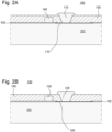
figures 2A and 2B illustrate a sectional view of a tamper-evident RFID Tag 100 according to a second embodiment; -
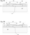
figures 3A and 3B depict a sectional view of a tamper-evident RFID Tag 100 according to a third embodiment; -
figures 4A and 4B show a sectional view of a tamper-evident RFID Tag 100 according to a fourth embodiment; -
figures 5, 5A & 5B represent an upper view and two sectional view of a tamper-evident RFID Tag 100 according to another embodiment; and, -
figure 6 illustrates a method for manufacturing 500 said Tamper-evident RFID Tag 100. - The present invention aims to overcome the drawbacks of the prior art via a Tamper-
evident RFID Tag 100, which may guaranty the origin of the product and may prevent any attempt of harvesting an assembly or a reassembly of said Tamper-evident RFID Tag 100. The latter, i.e. said tamper-evident RFID Tag 100 may comprise at least oneintegrated circuit 101, an insulatinglayer 102, at least oneprimary IC contact 110, and at least onesecondary IC contact 120 as illustrated infig. 5 for instance. - Said method 500 may comprises at least one main
electrical contact deposit 530 comprising at least one first mainelectrical contact deposit 531. Said at least one first mainelectrical contact deposit 531 may deposit at least one firstelectrical contact 130 and/or at least one secondelectrical contact 140 on said at least oneintegrated circuit 101. - As it can be construed from
fig. 5 , said at least one firstelectrical contact 130 may comprise at least one first proximalelectrical contact portion 131 configured to contact said at least oneprimary IC contact 110 and at least one first distalelectrical contact portion 132 configured to be near said at least onesecondary IC contact 120. Respectively, infig. 5 , said at least one secondelectrical contact 140 may comprise at least one second proximalelectrical contact portion 141 configured to contact said at least onesecondary IC contact 120 and at least one second distalelectrical contact portion 142 configured to be near said at least oneprimary IC contact 110.Fig. 5A may present a sectional view of a tamper-evident RFID Tag 100 showing how partly said at least onedegradable layer 155 may cover said tamper-evident RFID Tag 100 and uncover some test pad.Fig. 5B may illustrate how partly said at least onedegradable layer 155 may cover said tamper-evident RFID Tag 100, said at least one firstelectrical contact 130 and said at least one secondaryelectrical contact 140. Indeed, said at least one first distalelectrical contact portion 132 and said at least one second distalelectrical contact portion 142 may be covered whereas said at least one second proximalelectrical contact portion 141 and said at least one first proximalelectrical contact portion 131 may be not. - However, in some embodiments, there may only be said at least one first
electrical contact 130 or said at least one secondelectrical contact 140. - As depicted in
fig. 6 , said method 500 may comprise at least oneprotection layer deposit 540 of at least one protection layer 151 partly or totally on said at least oneintegrated circuit 101, and according to the embodiments, and on said at least one firstelectrical contact 130 and/or said at least one secondelectrical contact 140. Indeed, said at least one protection layer 151 may cover said at least one first distalelectrical contact portion 132 and/or said at least one second distalelectrical contact portion 142. - Further, at least one protection layer 151 may be provided 510 and may be deposited on said at least one
integrated circuit 101, on said at least one firstelectrical contact 130 and/or on said at least one secondelectrical contact 140. After said at least one providing 510 of said at least one protection layer 151, at least one curing 520 of said at least one protection layer 151 between 100°C and 200°C, preferably between 130°C and 170°C, during 2 minutes up to 45 minutes, preferably between 5 minutes and 15minutes, may occur such as to turn said at least one protection layer 151 into at least onedegradable layer 155. - Said at least one main
electrical contact deposit 530 may also comprise at least one second mainelectrical contact deposit 532 of said at least one firstelectrical contact 130 and/or of said at least one secondaryelectrical contact 140, if said at least one firstelectrical contact 130 and/or of said at least one secondaryelectrical contact 140 is or are not deposit during said at least one first mainelectrical contact deposit 531, on said at least oneintegrated circuit 101 and/or on said at least onedegradable layer 155. - Further, since said at least one protection layer 151 may be deposited in an early phase of method 500, said at least one protection layer 151 may be comprised between said at least one first distal
electrical contact portion 132 and said at least one second proximalelectrical contact portion 141 and/or said at least onesecondary IC contact 120, and/or to be comprised between said at least one second distalelectrical contact portion 142 and said at least one first proximalelectrical contact portion 131 and/or said at least oneprimary IC contact 110. - The same may be possible after said at least one protection layer 151 turns into said at least one
degradable layer 155, which means said at least onedegradable layer 155 may be comprised between said at least one first distalelectrical contact portion 132 and said at least one second proximalelectrical contact portion 141 and/or said at least onesecondary IC contact 120, and/or to be comprised between said at least one second distalelectrical contact portion 142 and said at least one first proximalelectrical contact portion 131 and/or said at least oneprimary IC contact 110. Therefore, said at least one first distalelectrical contact portion 132 may be disposed above said at least one second proximalelectrical contact portion 141 and/or said at least onesecondary IC contact 120 in some cases, and/or said at least one second distalelectrical contact portion 142 is configured to be disposed above said at least one first proximalelectrical contact portion 131 and/or said at least oneprimary IC contact 110 in some another cases. - As aforementioned in some the embodiments, there may be said at least one first
electrical contact 130 and/or said at least one secondelectrical contact 140, and said method 500 may comprise at least one auxiliaryelectrical contact deposit 550 comprising at least one first auxiliaryelectrical contact deposit 551 and/or at least one second auxiliaryelectrical contact deposit 552. - Said at least one first auxiliary
electrical contact deposit 551 may comprise a deposit of at least one primaryelectrical contact 115 and/or at least one secondaryelectrical contact 125 on said at least oneintegrated circuit 101 and/or on said at least onedegradable layer 155. Depending on the embodiments, said at least one second auxiliaryelectrical contact deposit 552 may comprise a deposit of at least one primaryelectrical contact 115 and/or at least one primaryelectrical contact 125 on said at least oneintegrated circuit 101 and/or on said at least onedegradable layer 155. In both case, said at least one primaryelectrical contact 115 and/or said at least one secondaryelectrical contact 125 may allow the electrical contact between the antenna and said at least oneprimary IC contact 110 and/or said at least onesecondary IC contact 120. Indeed, said at least one primaryelectrical contact 115 may contact said at least oneprimary IC contact 110 and/or said at least one firstelectrical contact 130, and/or said at least one secondaryelectrical contact 125 may contact said at least onesecondary IC contact 120 and/or said at least one secondelectrical contact 140. - As illustrated in
fig. 2 , said at least one primaryelectrical contact 115 and/or said at least one secondaryelectrical contact 125 may comprise at least one undercut such as to be disconnected of said at least oneprimary IC contact 110 and/or said at least onesecondary IC contact 120 respectively when said at least onedegradable layer 155 is altered and/or removed. - As it appears clearly from the present specification, any attempt of harvesting prevents an assembly or a reassembly of said Tamper-
evident RFID Tag 100, in particular with an antenna. Indeed, said at least one firstelectrical contact 130 and/or said at least one secondaryelectrical contact 140 may realize a short circuit with said at least onesecondary IC contact 120 and/or with said at least oneprimary IC contact 110 respectively. Indeed, if someone try to harvest said Tamper-evident RFID Tag 100, said antenna may be separate from said at least oneintegrated circuit 101 and said at least onedegradable layer 155 may be deteriorated, which leads to an exposure of said at least one first distalelectrical contact portion 132 and said at least onesecondary IC contact 120 or at least one second proximalelectrical contact portion 141 and/or of said at least one second distalelectrical contact portion 142 and said at least oneprimary IC contact 110 or said at least one first proximalelectrical contact portion 131. - If an assembly or a reassembly is attempted, a short circuit occurs due to the vicinity of said at least one distal
electrical contact portion IC contact electrical contact portion integrated circuit 101. -
Figure 1A and 1B illustrate a first embodiment, wherein said at least one firstelectrical contact 130 and at least one secondelectrical contact 140 may be disposed on said at least oneintegrated circuit 101. In this embodiment, said at least one first mainelectrical contact deposit 531 may deposit said at least one secondelectrical contact 140 contacting said at least onesecondary IC contact 120, more precisely, said at least one second proximalelectrical contact portion 141 may contact said at least onesecondary IC contact 120 and said at least one second distalelectrical contact portion 142 may be near said at least oneprimary IC contact 110. - Then, said at least one protection layer 151 may be deposited partly or totally on said at least one
integrated circuit 101, on said at least onesecondary IC contact 120, on said at least one second proximalelectrical contact portion 141 and on said at least one second distalelectrical contact portion 142. - Said at least one protection layer 151 may be cured 520 between 100°C and 200°C, preferably between 130°C and 170°C, during 2 minutes up to 45 minutes, preferably between 5 minutes and 15minutes, and may turn into at least one
degradable layer 155. - After that, said at least one first proximal
electrical contact portion 131 may be deposited on and may contact said at least oneprimary IC contact 110 and said at least one first distalelectrical contact portion 132 may be deposited on said at least onedegradable layer 155 and may be above said at least one second distalelectrical contact portion 142, and thus said at least one first distalelectrical contact portion 132 may be near said at least onesecondary IC contact 120. - In case, said Tamper-
evident RFID Tag 100 is mashed, said at least one second distalelectrical contact portion 142, and thus said at least one first distalelectrical contact portion 132 may create a short circuit between said at least oneprimary IC contact 110 and said at least onesecondary IC contact 120, and if said Tamper-evident RFID Tag 100 is peeled or harvested, said at least onedegradable layer 155 may be altered or removed with said at least one firstelectrical contact 130, and said at least one secondaryelectrical contact 140 and said at least oneprimary IC contact 110 may be revealed, and said at least oneintegrated circuit 101 may be inoperable. Since said at least one second distalelectrical contact portion 142 may be near or too close to said at least oneprimary IC contact 110, an assembly or a reassembly of said Tamper-evident RFID Tag 100 may be prevented and an antenna may be not soldered on said at least oneintegrated circuit 101 without short circuited said at least oneprimary IC contact 110 and said at least onesecondary IC contact 120 via said at least one second distalelectrical contact portion 142. - In
fig. 2A and 2B , said method for manufacturing 500 said Tamper-evident RFID Tag 100 may be slightly different. Indeed, said at least one secondelectrical contact 140 may be applied on said at least one secondary IC contact 120: said at least one second proximalelectrical contact portion 141 may contact said at least onesecondary IC contact 120 and said at least one second distalelectrical contact portion 142 may be near said at least oneprimary IC contact 110. Said at least one protection layer 151 may be deposited totally or partly on said at least oneintegrated circuit 101, before said at least one curing 520. - Then, said at least one first auxiliary
electrical contact deposit 551 may take place. Said at least one primaryelectrical contact 115 may be deposited on said at least oneintegrated circuit 101 and on said at least onedegradable layer 155. Indeed, said at least one primaryelectrical contact 115 may have said at least one undercut such as to be disconnected of said at least oneprimary IC contact 110 when said at least onedegradable layer 155 is altered and/or removed. Thus, said at least oneprimary IC contact 110 and said at least one second distalelectrical contact portion 142 may be uncovered such as to prevent an assembly or a reassembly of said Tamper-evident RFID Tag 100 by short circuiting said at least oneprimary IC contact 110 and said at least one second distalelectrical contact portion 142 and avoiding the soldering of an new antenna and rending said at least oneintegrated circuit 101 inoperable for example. Indeed, any attempt of harvesting prevents an assembly or a reassembly of said Tamper-evident RFID Tag 100 by altering said at least onedegradable layer 155 may prevent an assembly or a reassembly of said Tamper-evident RFID Tag 100 with an antenna due to a potential short circuit between said at least one first distalelectrical contact portion 132 and said at least onesecondary IC contact 120 and/or said at least one second distalelectrical contact portion 142 and said at least oneprimary IC contact 110. - Said tamper-
evident RFID Tag 100 of the third embodiment infig. 3A and 3B may be manufactured differently. Indeed, said at least one primaryelectrical contact 115 and said at least one secondelectrical contact 140, rather said at least one second proximalelectrical contact portion 141 and said at least one second distalelectrical contact portion 142 may be deposited on said at least oneintegrated circuit 101. Said at least one protection layer 151 may be deposited partly or totally on said at least oneintegrated circuit 101, said at least one primaryelectrical contact 115 and said at least one secondelectrical contact 140 and cured 520 such as to turn said at least one protection layer 151 into said at least onedegradable layer 155. In this third embodiment, said at least one second mainelectrical contact deposit 532 may occurs and said at least one firstelectrical contact 130 may be deposited on said at least onedegradable layer 155 as depicted infig. 3 . Said at least one firstelectrical contact 130 may contact said at least oneprimary IC contact 110 via said at least one primaryelectrical contact 115 and said at least one first proximalelectrical contact portion 131. Said at least one first distalelectrical contact portion 132 may be near said at least onesecondary IC contact 120 and above said at least one second distalelectrical contact portion 142. In this case, said at least one first distalelectrical contact portion 132 may be closer to said at least onesecondary IC contact 120 by being above said at least one second distalelectrical contact portion 142 then said at least one first proximalelectrical contact portion 131, said Tamper-evident RFID Tag 100 is mashed, said at least one second distalelectrical contact portion 142, and thus said at least one first distalelectrical contact portion 132 may create a short circuit between said at least oneprimary IC contact 110 and said at least onesecondary IC contact 120, and If said tamper-evident RFID Tag 100 is peeled or if there is an attempt to peel said tamper-evident RFID Tag 100, said at least onedegradable layer 155 may be degraded or removed taking away said at least one firstelectrical contact 130 and/or said at least one primaryelectrical contact 115 and thus said at least oneprimary IC contact 110 and said at least one second distalelectrical contact portion 142 may be uncovered such as to prevent an assembly or a reassembly of said Tamper-evident RFID Tag 100 by short circuiting said at least oneprimary IC contact 110 and said at least one second distalelectrical contact portion 142 and avoiding the soldering of an new antenna for example. -
Fig. 4A and 4B illustrate a fourth embodiment, wherein said at least one first mainelectrical contact deposit 531 may occurs and may deposit said at least one firstelectrical contact 130 and said at least one secondelectrical contact 140 on said at least oneintegrated circuit 101. After said at least one providing 510 of said at least one protection layer 151 and said at least one curing 520, such as to turn said at least one protection layer 151 into at least onedegradable layer 155, said at least one second auxiliaryelectrical contact deposit 552 may deposit said at least one primaryelectrical contact 115 on said at least one firstelectrical contact 130 and on said at least onedegradable layer 155. As it may be observed infig. 4 , said at least one primaryelectrical contact 115 may comprise said at least one undercut such as to take away said at least one firstelectrical contact 130 when said at least onedegradable layer 155 is altered and/or removed during the peeling of said tamper-evident RFID Tag 100. Thus said at least oneprimary IC contact 110 and said at least one second distalelectrical contact portion 142 may be uncovered such as to prevent an assembly or a reassembly of said Tamper-evident RFID Tag 100 by short circuiting said at least oneprimary IC contact 110 and said at least one second distalelectrical contact portion 142 and avoiding the soldering of an new antenna for example.
Claims (14)
- Method for manufacturing (500) a Tamper-evident RFID Tag (100); said method (500) comprising at least one:- Providing (510) of at least one protection layer (151); said at least one protection layer (151) being deposited on at least one integrated circuit (101);- Curing (520) said at least one protection layer (151) between 100°C and 200°C, preferably between 130°C and 170°C, during 2 minutes up to 45 minutes, preferably between 5 minutes and 15minutes, such as to turn said at least one protection layer (151) into at least one degradable layer (155).
- Method (500) according to claim 1, which comprises at least one main electrical contact deposit (530); said at least one main electrical contact deposit (530) comprises at least one:- first main electrical contact deposit (531); said at least one first main electrical contact deposit (531) comprises a deposit of at least one first electrical contact (130) and/or at least one second electrical contact (140) on said at least one integrated circuit (101) and/or on said at least one degradable layer (155); and/or- second main electrical contact deposit (532); said at least one second main electrical contact deposit (532) comprises a deposit of at least one first electrical contact (130) and/or at least one secondary electrical contact (140) on said at least one integrated circuit (101) and/or on said at least one degradable layer (155).
- Method (500) according to claim 1 or 2, which comprises at least one protection layer deposit (540); said at least one protection layer deposit (540) comprises a deposit of said at least one protection layer (151) on said at least one integrated circuit (101).
- Method (500) according to any of the preceding claims, which comprises at least one auxiliary electrical contact deposit (550); said at least one auxiliary electrical contact deposit (550) comprises at least one:- first auxiliary electrical contact deposit (551); said at least one first auxiliary electrical contact deposit (551) comprises a deposit of at least one primary electrical contact (115) and/or at least one secondary electrical contact (125) on said at least one integrated circuit (101) and/or on said at least one degradable layer (155); and/or- second auxiliary electrical contact deposit (552); said at least one second auxiliary electrical contact deposit (552) comprises a deposit of at least one primary electrical contact (115) and/or at least one primary electrical contact (125) on said at least one integrated circuit (101) and/or on said at least one degradable layer (155).
- Method (500) according to claim 3 or 4, wherein said at least one first main electrical contact deposit (531) occurs after said at least one protection layer deposit (540) and/or said at least one second main electrical contact deposit (532).
- Method (500) according to claim 3 or 4, wherein said at least one second main electrical contact deposit (532) occurs after said at least one protection layer deposit (540) and/or said at least one first main electrical contact deposit (531).
- Method (500) according to any of the preceding claims, wherein said at least one first auxiliary electrical contact deposit (551) occurs after said at least one protection layer deposit (540) and/or said at least one second auxiliary electrical contact deposit (552).
- Method (500) according to any of the preceding claims, wherein said at least one second auxiliary electrical contact deposit (552) occurs after said at least one protection layer deposit (540) and/or said at least one first auxiliary electrical contact deposit (551).
- Tamper-evident RFID Tag (100) comprising at least one integrated circuit (101), at least one primary IC contact (110), at least one secondary IC contact (120):- at least one first electrical contact (130): said at least one first electrical contact (130) comprising at least one first proximal electrical contact portion (131) configured to contact said at least one primary IC contact (110) and at least one first distal electrical contact portion (132) configured to be near said at least one secondary IC contact (120); and/or,- at least one second electrical contact (140): said at least one second electrical contact (140) comprising at least one second proximal electrical contact portion (141) configured to contact said at least one secondary IC contact (120) and at least one second distal electrical contact portion (142) configured to be near said at least one primary IC contact (110).
- Tamper-evident RFID Tag (100) according to claim 1, which comprises at least one degradable layer (155) configured to cover said at least one first distal electrical contact portion (132) and/or said at least one second distal electrical contact portion (142).
- Tamper-evident RFID Tag (100) according to claim 1 or 2, wherein said at least one degradable layer (155) is configured to be comprised between said at least one first distal electrical contact portion (132) and said at least one second proximal electrical contact portion (141) and/or said at least one secondary IC contact (120), and/or to be comprised between said at least one second distal electrical contact portion (142) and said at least one first proximal electrical contact portion (131) and/or said at least one primary IC contact (110).
- Tamper-evident RFID Tag (100) according to any of the preceding claims, wherein said at least one first distal electrical contact portion (132) is configured to be disposed above said at least one second proximal electrical contact portion (141) and/or said at least one secondary IC contact (120), and/or said at least one second distal electrical contact portion (142) is configured to be disposed above said at least one first proximal electrical contact portion (131) and/or said at least one primary IC contact (110).
- Tamper-evident RFID Tag (100) according to any of the preceding claims, which comprises at least one primary electrical contact (115) configured to contact said at least one primary IC contact (110) and/or said at least one first electrical contact (130), and/or at least one secondary electrical contact (125) configured to contact said at least one secondary IC contact (120) and/or said at least one second electrical contact (140).
- Tamper-evident RFID Tag (100) according to claim 13, wherein said at least one primary electrical contact (115) and/or said at least one secondary electrical contact (125) comprises or comprise at least one undercut such as to be disconnected of said at least one primary IC contact (110) and/or said at least one secondary IC contact (120) respectively when said at least one degradable layer (155) is altered and/or removed.
Priority Applications (2)
| Application Number | Priority Date | Filing Date | Title |
|---|---|---|---|
| EP21218213.3A EP4206985A1 (en) | 2021-12-29 | 2021-12-29 | Tamper-evident rfid tag and method thereof |
| US18/085,770 US12353940B2 (en) | 2021-12-29 | 2022-12-21 | Tamper-evident RFID tag and method thereof |
Applications Claiming Priority (1)
| Application Number | Priority Date | Filing Date | Title |
|---|---|---|---|
| EP21218213.3A EP4206985A1 (en) | 2021-12-29 | 2021-12-29 | Tamper-evident rfid tag and method thereof |
Publications (1)
| Publication Number | Publication Date |
|---|---|
| EP4206985A1 true EP4206985A1 (en) | 2023-07-05 |
Family
ID=79024841
Family Applications (1)
| Application Number | Title | Priority Date | Filing Date |
|---|---|---|---|
| EP21218213.3A Pending EP4206985A1 (en) | 2021-12-29 | 2021-12-29 | Tamper-evident rfid tag and method thereof |
Country Status (2)
| Country | Link |
|---|---|
| US (1) | US12353940B2 (en) |
| EP (1) | EP4206985A1 (en) |
Citations (8)
| Publication number | Priority date | Publication date | Assignee | Title |
|---|---|---|---|---|
| US20060092028A1 (en) * | 2004-10-08 | 2006-05-04 | Proximities, Inc. | Identification band using shorting wire for enabling/disabling an RFID transponder contained thereon |
| FR2890213A1 (en) * | 2005-08-31 | 2007-03-02 | Francois Charles Oberthur Fidu | Identity and security document e.g. passport, has sheet whose reverse side is fixed to recto side of additional sheet to enclose non-contact silicon chip between two sheets, where reverse side of additional sheet is covered with adhesive |
| US20110169611A1 (en) * | 2008-11-25 | 2011-07-14 | Hood David Macintosh | Laminate tamper evident construct |
| US20140239074A1 (en) * | 2011-06-02 | 2014-08-28 | Gang Wang | Method of designing & manufacturing an anti-counterfeiting rfid tag, the anti-counterfeiting rfid tag and the anti-counterfeiting package |
| US20140326790A1 (en) * | 2011-09-05 | 2014-11-06 | Shanghai Techsun Rfid Technology Co., Ltd. | Radio frequency identification tag having diversion-proof function and manufacturing method thereof |
| CN206946532U (en) * | 2017-06-14 | 2018-01-30 | 中山金利宝胶粘制品有限公司 | A kind of tamper-evident RFID Anti-fake electronic labels |
| CN108596323A (en) * | 2018-06-25 | 2018-09-28 | 武汉天喻聚联网络有限公司 | A kind of passive anti-RFID adhesive tapes torn |
| US20200279143A1 (en) * | 2019-02-18 | 2020-09-03 | Compx International Inc. | Medicinal dosage storage and method for combined electronic inventory data and access control |
Family Cites Families (2)
| Publication number | Priority date | Publication date | Assignee | Title |
|---|---|---|---|---|
| EP0940652B1 (en) * | 1998-03-05 | 2004-12-22 | Nippon Telegraph and Telephone Corporation | Surface shape recognition sensor and method of fabricating the same |
| US7723162B2 (en) * | 2002-03-22 | 2010-05-25 | White Electronic Designs Corporation | Method for producing shock and tamper resistant microelectronic devices |
-
2021
- 2021-12-29 EP EP21218213.3A patent/EP4206985A1/en active Pending
-
2022
- 2022-12-21 US US18/085,770 patent/US12353940B2/en active Active
Patent Citations (8)
| Publication number | Priority date | Publication date | Assignee | Title |
|---|---|---|---|---|
| US20060092028A1 (en) * | 2004-10-08 | 2006-05-04 | Proximities, Inc. | Identification band using shorting wire for enabling/disabling an RFID transponder contained thereon |
| FR2890213A1 (en) * | 2005-08-31 | 2007-03-02 | Francois Charles Oberthur Fidu | Identity and security document e.g. passport, has sheet whose reverse side is fixed to recto side of additional sheet to enclose non-contact silicon chip between two sheets, where reverse side of additional sheet is covered with adhesive |
| US20110169611A1 (en) * | 2008-11-25 | 2011-07-14 | Hood David Macintosh | Laminate tamper evident construct |
| US20140239074A1 (en) * | 2011-06-02 | 2014-08-28 | Gang Wang | Method of designing & manufacturing an anti-counterfeiting rfid tag, the anti-counterfeiting rfid tag and the anti-counterfeiting package |
| US20140326790A1 (en) * | 2011-09-05 | 2014-11-06 | Shanghai Techsun Rfid Technology Co., Ltd. | Radio frequency identification tag having diversion-proof function and manufacturing method thereof |
| CN206946532U (en) * | 2017-06-14 | 2018-01-30 | 中山金利宝胶粘制品有限公司 | A kind of tamper-evident RFID Anti-fake electronic labels |
| CN108596323A (en) * | 2018-06-25 | 2018-09-28 | 武汉天喻聚联网络有限公司 | A kind of passive anti-RFID adhesive tapes torn |
| US20200279143A1 (en) * | 2019-02-18 | 2020-09-03 | Compx International Inc. | Medicinal dosage storage and method for combined electronic inventory data and access control |
Also Published As
| Publication number | Publication date |
|---|---|
| US20230206022A1 (en) | 2023-06-29 |
| US12353940B2 (en) | 2025-07-08 |
Similar Documents
| Publication | Publication Date | Title |
|---|---|---|
| US7277017B2 (en) | RFID tag | |
| US8444058B2 (en) | Embedded RFID tags and associated methods and systems | |
| EP0905657B1 (en) | Currency note comprising an integrated circuit | |
| US8334757B2 (en) | Controlling data access to and from an RFID device | |
| US8395504B2 (en) | IC label for prevention of forgery | |
| KR101003322B1 (en) | How to make smart labels that can be laser engraved and adhesive | |
| US20080073437A1 (en) | Method for operating an authenticity tag | |
| US20140239074A1 (en) | Method of designing & manufacturing an anti-counterfeiting rfid tag, the anti-counterfeiting rfid tag and the anti-counterfeiting package | |
| AU2002337402B2 (en) | Thin electronic label and method for making same | |
| EP1179811A1 (en) | Security document and process for producing a security document | |
| JP2002536727A (en) | Integrated circuit | |
| CN110533144B (en) | Chip for RFID electronic tag, RFID electronic tag and method for preventing chip transfer | |
| WO2007093039A1 (en) | A secure gaming chip | |
| WO2008011254A2 (en) | Electrostatic discharge protection for components of an rfid tag | |
| US12353940B2 (en) | Tamper-evident RFID tag and method thereof | |
| US20190138874A1 (en) | Rfid-based indicator for use with fastening substrates and related methods | |
| JPS59109397A (en) | How to improve security against counterfeiting of identification cards | |
| US8742931B2 (en) | Electronic seal with multiple means of identification and method based on electronic seal for inspecting goods | |
| RU182178U1 (en) | CRYPTOGRAPHIC LABEL | |
| US10839177B2 (en) | Radiofrequency tag device, corresponding assembly and method | |
| CN111753933B (en) | Chip anti-transfer detection method of passive RFID tag, computer device and computer readable storage medium | |
| US10360491B2 (en) | Method for providing random combination status code for commodity | |
| EP1769468A1 (en) | Security paper and articles comprising such paper | |
| WO2009083367A1 (en) | Safety component having film arrangement | |
| WO2009112999A1 (en) | Rf identification tag |
Legal Events
| Date | Code | Title | Description |
|---|---|---|---|
| PUAI | Public reference made under article 153(3) epc to a published international application that has entered the european phase |
Free format text: ORIGINAL CODE: 0009012 |
|
| STAA | Information on the status of an ep patent application or granted ep patent |
Free format text: STATUS: THE APPLICATION HAS BEEN PUBLISHED |
|
| AK | Designated contracting states |
Kind code of ref document: A1 Designated state(s): AL AT BE BG CH CY CZ DE DK EE ES FI FR GB GR HR HU IE IS IT LI LT LU LV MC MK MT NL NO PL PT RO RS SE SI SK SM TR |
|
| P01 | Opt-out of the competence of the unified patent court (upc) registered |
Effective date: 20231109 |
|
| STAA | Information on the status of an ep patent application or granted ep patent |
Free format text: STATUS: REQUEST FOR EXAMINATION WAS MADE |
|
| 17P | Request for examination filed |
Effective date: 20240104 |
|
| RBV | Designated contracting states (corrected) |
Designated state(s): AL AT BE BG CH CY CZ DE DK EE ES FI FR GB GR HR HU IE IS IT LI LT LU LV MC MK MT NL NO PL PT RO RS SE SI SK SM TR |
|
| STAA | Information on the status of an ep patent application or granted ep patent |
Free format text: STATUS: EXAMINATION IS IN PROGRESS |
|
| 17Q | First examination report despatched |
Effective date: 20250124 |