EP4206803A1 - Liquid crystal display device - Google Patents
Liquid crystal display device Download PDFInfo
- Publication number
- EP4206803A1 EP4206803A1 EP22208124.2A EP22208124A EP4206803A1 EP 4206803 A1 EP4206803 A1 EP 4206803A1 EP 22208124 A EP22208124 A EP 22208124A EP 4206803 A1 EP4206803 A1 EP 4206803A1
- Authority
- EP
- European Patent Office
- Prior art keywords
- liquid crystal
- support
- cover
- crystal display
- display device
- Prior art date
- Legal status (The legal status is an assumption and is not a legal conclusion. Google has not performed a legal analysis and makes no representation as to the accuracy of the status listed.)
- Granted
Links
Images


Classifications
-
- G—PHYSICS
- G02—OPTICS
- G02F—OPTICAL DEVICES OR ARRANGEMENTS FOR THE CONTROL OF LIGHT BY MODIFICATION OF THE OPTICAL PROPERTIES OF THE MEDIA OF THE ELEMENTS INVOLVED THEREIN; NON-LINEAR OPTICS; FREQUENCY-CHANGING OF LIGHT; OPTICAL LOGIC ELEMENTS; OPTICAL ANALOGUE/DIGITAL CONVERTERS
- G02F1/00—Devices or arrangements for the control of the intensity, colour, phase, polarisation or direction of light arriving from an independent light source, e.g. switching, gating or modulating; Non-linear optics
- G02F1/01—Devices or arrangements for the control of the intensity, colour, phase, polarisation or direction of light arriving from an independent light source, e.g. switching, gating or modulating; Non-linear optics for the control of the intensity, phase, polarisation or colour
- G02F1/13—Devices or arrangements for the control of the intensity, colour, phase, polarisation or direction of light arriving from an independent light source, e.g. switching, gating or modulating; Non-linear optics for the control of the intensity, phase, polarisation or colour based on liquid crystals, e.g. single liquid crystal display cells
- G02F1/133—Constructional arrangements; Operation of liquid crystal cells; Circuit arrangements
- G02F1/1333—Constructional arrangements; Manufacturing methods
- G02F1/133308—Support structures for LCD panels, e.g. frames or bezels
-
- G—PHYSICS
- G02—OPTICS
- G02F—OPTICAL DEVICES OR ARRANGEMENTS FOR THE CONTROL OF LIGHT BY MODIFICATION OF THE OPTICAL PROPERTIES OF THE MEDIA OF THE ELEMENTS INVOLVED THEREIN; NON-LINEAR OPTICS; FREQUENCY-CHANGING OF LIGHT; OPTICAL LOGIC ELEMENTS; OPTICAL ANALOGUE/DIGITAL CONVERTERS
- G02F1/00—Devices or arrangements for the control of the intensity, colour, phase, polarisation or direction of light arriving from an independent light source, e.g. switching, gating or modulating; Non-linear optics
- G02F1/01—Devices or arrangements for the control of the intensity, colour, phase, polarisation or direction of light arriving from an independent light source, e.g. switching, gating or modulating; Non-linear optics for the control of the intensity, phase, polarisation or colour
- G02F1/13—Devices or arrangements for the control of the intensity, colour, phase, polarisation or direction of light arriving from an independent light source, e.g. switching, gating or modulating; Non-linear optics for the control of the intensity, phase, polarisation or colour based on liquid crystals, e.g. single liquid crystal display cells
- G02F1/133—Constructional arrangements; Operation of liquid crystal cells; Circuit arrangements
- G02F1/1333—Constructional arrangements; Manufacturing methods
- G02F1/133308—Support structures for LCD panels, e.g. frames or bezels
- G02F1/133317—Intermediate frames, e.g. between backlight housing and front frame
-
- G—PHYSICS
- G02—OPTICS
- G02F—OPTICAL DEVICES OR ARRANGEMENTS FOR THE CONTROL OF LIGHT BY MODIFICATION OF THE OPTICAL PROPERTIES OF THE MEDIA OF THE ELEMENTS INVOLVED THEREIN; NON-LINEAR OPTICS; FREQUENCY-CHANGING OF LIGHT; OPTICAL LOGIC ELEMENTS; OPTICAL ANALOGUE/DIGITAL CONVERTERS
- G02F1/00—Devices or arrangements for the control of the intensity, colour, phase, polarisation or direction of light arriving from an independent light source, e.g. switching, gating or modulating; Non-linear optics
- G02F1/01—Devices or arrangements for the control of the intensity, colour, phase, polarisation or direction of light arriving from an independent light source, e.g. switching, gating or modulating; Non-linear optics for the control of the intensity, phase, polarisation or colour
- G02F1/13—Devices or arrangements for the control of the intensity, colour, phase, polarisation or direction of light arriving from an independent light source, e.g. switching, gating or modulating; Non-linear optics for the control of the intensity, phase, polarisation or colour based on liquid crystals, e.g. single liquid crystal display cells
- G02F1/133—Constructional arrangements; Operation of liquid crystal cells; Circuit arrangements
- G02F1/1333—Constructional arrangements; Manufacturing methods
- G02F1/133308—Support structures for LCD panels, e.g. frames or bezels
- G02F1/133314—Back frames
-
- G—PHYSICS
- G02—OPTICS
- G02F—OPTICAL DEVICES OR ARRANGEMENTS FOR THE CONTROL OF LIGHT BY MODIFICATION OF THE OPTICAL PROPERTIES OF THE MEDIA OF THE ELEMENTS INVOLVED THEREIN; NON-LINEAR OPTICS; FREQUENCY-CHANGING OF LIGHT; OPTICAL LOGIC ELEMENTS; OPTICAL ANALOGUE/DIGITAL CONVERTERS
- G02F1/00—Devices or arrangements for the control of the intensity, colour, phase, polarisation or direction of light arriving from an independent light source, e.g. switching, gating or modulating; Non-linear optics
- G02F1/01—Devices or arrangements for the control of the intensity, colour, phase, polarisation or direction of light arriving from an independent light source, e.g. switching, gating or modulating; Non-linear optics for the control of the intensity, phase, polarisation or colour
- G02F1/13—Devices or arrangements for the control of the intensity, colour, phase, polarisation or direction of light arriving from an independent light source, e.g. switching, gating or modulating; Non-linear optics for the control of the intensity, phase, polarisation or colour based on liquid crystals, e.g. single liquid crystal display cells
- G02F1/133—Constructional arrangements; Operation of liquid crystal cells; Circuit arrangements
- G02F1/1333—Constructional arrangements; Manufacturing methods
- G02F1/133308—Support structures for LCD panels, e.g. frames or bezels
- G02F1/133322—Mechanical guidance or alignment of LCD panel support components
-
- G—PHYSICS
- G02—OPTICS
- G02F—OPTICAL DEVICES OR ARRANGEMENTS FOR THE CONTROL OF LIGHT BY MODIFICATION OF THE OPTICAL PROPERTIES OF THE MEDIA OF THE ELEMENTS INVOLVED THEREIN; NON-LINEAR OPTICS; FREQUENCY-CHANGING OF LIGHT; OPTICAL LOGIC ELEMENTS; OPTICAL ANALOGUE/DIGITAL CONVERTERS
- G02F1/00—Devices or arrangements for the control of the intensity, colour, phase, polarisation or direction of light arriving from an independent light source, e.g. switching, gating or modulating; Non-linear optics
- G02F1/01—Devices or arrangements for the control of the intensity, colour, phase, polarisation or direction of light arriving from an independent light source, e.g. switching, gating or modulating; Non-linear optics for the control of the intensity, phase, polarisation or colour
- G02F1/13—Devices or arrangements for the control of the intensity, colour, phase, polarisation or direction of light arriving from an independent light source, e.g. switching, gating or modulating; Non-linear optics for the control of the intensity, phase, polarisation or colour based on liquid crystals, e.g. single liquid crystal display cells
- G02F1/133—Constructional arrangements; Operation of liquid crystal cells; Circuit arrangements
- G02F1/1333—Constructional arrangements; Manufacturing methods
- G02F1/1335—Structural association of cells with optical devices, e.g. polarisers or reflectors
- G02F1/1336—Illuminating devices
-
- G—PHYSICS
- G02—OPTICS
- G02F—OPTICAL DEVICES OR ARRANGEMENTS FOR THE CONTROL OF LIGHT BY MODIFICATION OF THE OPTICAL PROPERTIES OF THE MEDIA OF THE ELEMENTS INVOLVED THEREIN; NON-LINEAR OPTICS; FREQUENCY-CHANGING OF LIGHT; OPTICAL LOGIC ELEMENTS; OPTICAL ANALOGUE/DIGITAL CONVERTERS
- G02F1/00—Devices or arrangements for the control of the intensity, colour, phase, polarisation or direction of light arriving from an independent light source, e.g. switching, gating or modulating; Non-linear optics
- G02F1/01—Devices or arrangements for the control of the intensity, colour, phase, polarisation or direction of light arriving from an independent light source, e.g. switching, gating or modulating; Non-linear optics for the control of the intensity, phase, polarisation or colour
- G02F1/13—Devices or arrangements for the control of the intensity, colour, phase, polarisation or direction of light arriving from an independent light source, e.g. switching, gating or modulating; Non-linear optics for the control of the intensity, phase, polarisation or colour based on liquid crystals, e.g. single liquid crystal display cells
- G02F1/133—Constructional arrangements; Operation of liquid crystal cells; Circuit arrangements
- G02F1/1333—Constructional arrangements; Manufacturing methods
- G02F1/1335—Structural association of cells with optical devices, e.g. polarisers or reflectors
- G02F1/1336—Illuminating devices
- G02F1/133602—Direct backlight
- G02F1/133606—Direct backlight including a specially adapted diffusing, scattering or light controlling members
-
- G—PHYSICS
- G02—OPTICS
- G02F—OPTICAL DEVICES OR ARRANGEMENTS FOR THE CONTROL OF LIGHT BY MODIFICATION OF THE OPTICAL PROPERTIES OF THE MEDIA OF THE ELEMENTS INVOLVED THEREIN; NON-LINEAR OPTICS; FREQUENCY-CHANGING OF LIGHT; OPTICAL LOGIC ELEMENTS; OPTICAL ANALOGUE/DIGITAL CONVERTERS
- G02F1/00—Devices or arrangements for the control of the intensity, colour, phase, polarisation or direction of light arriving from an independent light source, e.g. switching, gating or modulating; Non-linear optics
- G02F1/01—Devices or arrangements for the control of the intensity, colour, phase, polarisation or direction of light arriving from an independent light source, e.g. switching, gating or modulating; Non-linear optics for the control of the intensity, phase, polarisation or colour
- G02F1/13—Devices or arrangements for the control of the intensity, colour, phase, polarisation or direction of light arriving from an independent light source, e.g. switching, gating or modulating; Non-linear optics for the control of the intensity, phase, polarisation or colour based on liquid crystals, e.g. single liquid crystal display cells
- G02F1/133—Constructional arrangements; Operation of liquid crystal cells; Circuit arrangements
- G02F1/1333—Constructional arrangements; Manufacturing methods
- G02F1/1335—Structural association of cells with optical devices, e.g. polarisers or reflectors
- G02F1/1336—Illuminating devices
- G02F1/133602—Direct backlight
- G02F1/133608—Direct backlight including particular frames or supporting means
-
- G—PHYSICS
- G02—OPTICS
- G02F—OPTICAL DEVICES OR ARRANGEMENTS FOR THE CONTROL OF LIGHT BY MODIFICATION OF THE OPTICAL PROPERTIES OF THE MEDIA OF THE ELEMENTS INVOLVED THEREIN; NON-LINEAR OPTICS; FREQUENCY-CHANGING OF LIGHT; OPTICAL LOGIC ELEMENTS; OPTICAL ANALOGUE/DIGITAL CONVERTERS
- G02F1/00—Devices or arrangements for the control of the intensity, colour, phase, polarisation or direction of light arriving from an independent light source, e.g. switching, gating or modulating; Non-linear optics
- G02F1/01—Devices or arrangements for the control of the intensity, colour, phase, polarisation or direction of light arriving from an independent light source, e.g. switching, gating or modulating; Non-linear optics for the control of the intensity, phase, polarisation or colour
- G02F1/13—Devices or arrangements for the control of the intensity, colour, phase, polarisation or direction of light arriving from an independent light source, e.g. switching, gating or modulating; Non-linear optics for the control of the intensity, phase, polarisation or colour based on liquid crystals, e.g. single liquid crystal display cells
- G02F1/133—Constructional arrangements; Operation of liquid crystal cells; Circuit arrangements
- G02F1/1333—Constructional arrangements; Manufacturing methods
- G02F1/133308—Support structures for LCD panels, e.g. frames or bezels
- G02F1/133325—Assembling processes
-
- G—PHYSICS
- G02—OPTICS
- G02F—OPTICAL DEVICES OR ARRANGEMENTS FOR THE CONTROL OF LIGHT BY MODIFICATION OF THE OPTICAL PROPERTIES OF THE MEDIA OF THE ELEMENTS INVOLVED THEREIN; NON-LINEAR OPTICS; FREQUENCY-CHANGING OF LIGHT; OPTICAL LOGIC ELEMENTS; OPTICAL ANALOGUE/DIGITAL CONVERTERS
- G02F2201/00—Constructional arrangements not provided for in groups G02F1/00 - G02F7/00
- G02F2201/46—Fixing elements
Definitions
- the present disclosure relates to a display device, and more particularly, to a liquid crystal display device having a narrow bezel.
- FPD flat panel display devices
- LCD liquid crystal display devices
- OLED organic light emitting diode display devices
- liquid crystal display devices have been widely used because of their compact size, light weight, thin thickness, low power driving, and the like.
- the liquid crystal display devices use optical anisotropy and dielectric anisotropy of liquid crystal and include two substrates, a liquid crystal layer between the two substrates, and a pixel electrode and a common electrode for driving liquid crystal molecules of the liquid crystal layer.
- the liquid crystal display devices control the arrangement of the liquid crystal molecules by an electric field generated by applying a voltage to the pixel electrode and the common electrode and display images by the light transmittance changed accordingly.
- the liquid crystal display devices have been widely applied to portable devices such as cellphones or multimedia devices, monitors for notebooks or computers, and large televisions.
- the present disclosure is directed to a liquid crystal display device that substantially obviates one or more of the problems due to limitations and disadvantages described above. to a liquid crystal display device with a minimized bezel.
- a liquid crystal display device includes a cover bottom including a first cover portion of a first direction and a second cover portion of a second direction; a backlight unit over the cover bottom and including a light source, a diffusion plate, and an optical sheet; a support main maintaining a distance between the light source and the diffusion plate and including a first support portion and a second support portion; and a liquid crystal panel over the backlight unit and the support main, wherein the support main and the cover bottom are combined with each other by a plurality of screws, and wherein the first cover portion includes a plurality of protrusions protruding outward from an outer surface of the second cover portion and corresponding to the plurality of screws, respectively.
- the support main may be also called support main structure.
- the second cover portion may disposed between adjacent protrusions.
- the first cover portion may have a cover groove between the second cover portion and one of the plurality of protrusions.
- the first support portion may have a first support groove corresponding to the second cover portion.
- each protrusion may be disposed between adjacent first support grooves.
- the first support portion may further have a second support groove corresponding to an edge of the light source.
- the plurality of protrusions may protrude outward from an outer surface of the second support portion.
- the liquid crystal display device may further comprise a guide panel between the backlight unit and the liquid crystal panel.
- the guide panel may include a first guide portion extending in the first direction and a second guide portion extending in the second direction.
- the plurality of protrusions may partially overlap the second guide portion.
- the first cover portion may have a cover hole corresponding to each screw.
- the first support portion may have a support hole corresponding to the cover hole.
- a press-fit nut may be is provided in the cover hole and the support hole.
- the support hole may have a first hole part and a second hole part.
- an area of the first hole part may be larger than an area of the second hole part.
- an inner side of the first hole part may be is opened.
- FIG. 1 and FIG. 2 are schematic cross-sectional views of a LCD device of an embodiment of the present disclosure
- FIG. 3 is a top perspective view of the LCD device of the embodiment of the present disclosure
- FIG. 4 is a bottom perspective view of the liquid crystal display device of the embodiment of the present disclosure.
- FIGS. 1 , 3, and 4 show a part with a screw joint structure
- FIG. 2 shows a part without a screw joint structure.
- FIG. 5 and FIG. 6 are a top perspective view and a bottom perspective view schematically showing a configuration between a cover bottom and a support main of the liquid crystal display device of the embodiment of the present disclosure, respectively, and show the part with the screw joint structure.
- the liquid crystal display device of the embodiment of the present disclosure includes a liquid crystal panel 100, a backlight unit 200, an adhesive member 300, a guide panel 400, a support main 500, and a cover bottom 600.
- the support main 500 and the cover bottom 600 are combined with each other by a screw 800.
- the support main 500 may be also called support main structure 500.
- the liquid crystal panel 100 includes a first substrate 110 in a lower position and a second substrate 120 in an upper position, and a liquid crystal layer (not shown) is interposed between the first and second substrates 110 and 120.
- the first substrate 110 includes a plurality of gate lines and a plurality of data lines on an inner surface thereof.
- the gate lines and the data lines cross each other to define a plurality of pixel regions.
- a thin film transistor, a pixel electrode, and a common electrode are provided in each pixel region.
- the thin film transistor is connected to the corresponding gate line and the corresponding data line, and the pixel electrode is connected to the thin film transistor.
- the pixel electrode and the common electrode generate an electric field to drive liquid crystal molecules of the liquid crystal layer.
- This first substrate 110 may be referred to as an array substrate.
- the second substrate 120 includes a black matrix, a color filter layer, and an overcoat layer on an inner surface thereof.
- the color filter layer includes red, green, and blue color filters
- the black matrix has openings corresponding to respective pixel regions.
- the red, green, and blue color filters of the color filter layer are disposed to correspond to the opening, respectively.
- This second substrate 120 may be referred to as a color filter substrate.
- a side sealing member 150 is provided at side or lateral surfaces of the first and second substrates 110 and 120.
- the side sealing member 150 may be formed of a material absorbing light.
- the side sealing member 150 can prevent light leakage occurring at side surfaces of the liquid crystal panel 100. More specifically, some of light outputted from the liquid crystal panel 100 travel toward the side surfaces of the liquid crystal panel 100.
- the side sealing member 150 is provided at the side surfaces of the liquid crystal panel 100, thereby blocking the light leakage due to the light traveling toward the side surfaces of the liquid crystal panel 100.
- the side sealing member 150 protects the side surfaces of the liquid crystal panel 100 from external impacts.
- the liquid crystal panel 100 further includes a first polarizer 130 and a second polarizer 140.
- the first polarizer 130 is attached to an outer surface of the first substrate 110, that is, a lower surface of the first substrate 110
- the second polarizer 140 is attached to an outer surface of the second substrate 120, that is, an upper surface of the second substrate 120 in the context of the figures.
- the first polarizer 130 is disposed under the first substrate 110, and the second polarizer 140 is disposed over the second substrate 120.
- the first polarizer 130 and the second polarizer 140 transmit linearly-polarized light only parallel to respective transmission axes.
- the transmission axis of the first polarizer 130 is perpendicular to the transmission axis of the second polarizer 140.
- One of the first and second polarizer 130, 140 might be omitted.
- a size of the second polarizer 140 is larger than a size of the first polarizer 130. Accordingly, the first polarizer 130 may be spaced apart from the side sealing member 150, and the second polarizer 140 may be in contact with the side sealing member 150.
- the size of the first polarizer 130 is smaller than a size of the first substrate 110, and the outer surface of the first substrate 110 is partially exposed. More specifically, the outer surface of the first substrate 110 is exposed between an edge of the first polarizer 130 and an edge of the first substrate 110.
- the backlight unit 200 is disposed under the liquid crystal panel 100 to provide light to the liquid crystal panel 100.
- the backlight unit 200 includes a light emitting diode (LED) array 210, a reflection plate 220, a diffusion plate 230, and an optical sheet 240.
- LED light emitting diode
- the backlight unit 200 is a direct type in which the LED array 210 of a light source is disposed right under the liquid crystal panel 100.
- the LED array 210 may include a plurality of LEDs 212.
- the LEDs might be provided on a printed circuit board (PCB).
- PCB printed circuit board
- each LED 212 may be a mini LED having a size of 100 to 200 ⁇ m. Accordingly, by implementing the local dimming in which light is selectively provided to the liquid crystal panel 100 by zones, the black luminance is improved, so that the contrast ratio can be increased and the power consumption can be decreased.
- the present disclosure is not limited thereto, and various sizes and types of LEDs can be applied.
- the reflection plate 220 is provided on the LED array 210.
- the reflection plate 220 has openings corresponding to the LEDs 212, and the LEDs 212 are arranged in the respective openings. Accordingly, light from the LEDs 212 travels toward the liquid crystal panel 100, and light reflected by the liquid crystal panel 100 or other components over the LEDs 212 and traveling toward the reflection plate 220 is reflected by the reflection plate 220 again and then is sent back to the liquid crystal panel 100, thereby increasing the light efficiency.
- the diffusion plate 230 is disposed over the reflection plate 220.
- the diffusion plate 230 is spaced apart from the LED array 210 and the reflection plate 220 with a predetermined distance and uniformly diffuses light from the LEDs 212.
- the distance between the reflection plate 220 and the diffusion plate 230 is larger than the distance between optical sheet 240 and the lower polarizer 130.
- the optical sheet 240 is disposed over the diffusion plate 230.
- the optical sheet 240 may include at least one diffusion sheet and at least one light-concentrating sheet such that more uniform surface light source can be incident on the liquid crystal panel 100 by diffusion or concentrating light passing through the diffusion plate 230.
- the optical sheet 240 may include two light-concentrating sheets and one diffusion sheet sequentially disposed over the diffusion plate 230.
- the light-concentrating sheets may include prism patterns or lenticular patterns.
- one of the light-concentrating sheets may include lenticular patterns, and the other may include prism patterns.
- the optical sheet 240 may further include a brightness enhancement film in which layers having different refractive indexes are alternately stacked or may the brightness enhancement film instead of the diffusion sheet.
- the liquid crystal panel 100 and the backlight unit 200 are fastened and supported by the guide panel 400, the support main 500, and the cover bottom 600.
- the liquid crystal panel 100 is fastened on the guide panel 400.
- the guide panel 400 may be formed along edges of the liquid crystal panel 100, thereby having a plane structure of a substantially square or rectangular frame shape.
- the guide panel 400 includes a first guide portion 410 and a second guide portion 420.
- the first guide portion 410 may be a horizontal portion extending in an X direction
- the second guide portion 420 may be a vertical portion extending in a Z direction.
- One side end of the first guide portion 410 may be connected to an upper end of the second guide portion 420, and the guide panel 400 may have a substantially L- shaped cross-section. Meanwhile, the other side end of the first guide 410 may protrude toward the Z direction. That is, the first guide 410 may have a protrusion on at the other side end.
- the adhesive member 300 is proved between the first guide portion 410 of the guide panel 400 and the liquid crystal panel 100, in particular the edge of the liquid crystal panel 100, so that the liquid crystal panel 100 may be fixed to the first guide portion 410 by the adhesive member 300.
- the adhesive member 300 overlaps and contacts the exposed lower surface of the first substrate 110 and also overlaps and contacts at least partly the first polarizer 130.
- the adhesive member 300 may be a foam pad having a cushioned property, and thus, the adhesive member 300 may act as a buffer absorbing external impacts.
- the adhesive member 300 may be formed of an elastic material and for example, formed of polyethylene, polyacryl, or polyurethane. However, the present disclosure is not limited thereto.
- the support main 500 is disposed under the guide panel 400.
- the support main 500 may be formed along the edges of the liquid crystal panel 100, thereby having a plane structure of a substantially square or rectangular frame shape.
- the support main 500 includes a first support portion 510 and a second support portion 520.
- the first support portion 510 is disposed between the reflection plate 220 and the diffusion plate 230.
- the second support portion 520 extends from an upper surface of an edge of the first support portion 510 toward the Z direction and surrounds side surfaces of the diffusion plate 230 and the optical sheet 240.
- the second support portion 520 is disposed between the side surfaces of the diffusion plate 230 and the optical sheet 240 and the second guide portion 420 of the guide panel 400.
- the first support portion 510 maintains a certain distance between the LED array 210 and the diffusion plate 230 so that light from the LEDs 212 may be mixed to implement uniform surface light source.
- the diffusion plate 230 is disposed on the first support portion 510. Accordingly, the diffusion plate 230 and the optical sheet 240 are disposed between the first support portion 510 and the first guide portion 410, and the upper surface of the first support portion 510 is in contact with a lower surface of the diffusion plate 230, thereby supporting the diffusion plate 230 and the optical sheet 240.
- An outer surface of the first support portion 510 is adjacent to the second guide portion 420 of the guide panel 400 and is surrounded by the second guide portion 420.
- An inner surface of the first support portion 520 has an inclination. That is, the first support portion 510 has an inclined surface 510a on the inner side. The inclined surface 510a reflects light from the LEDs 212 and sends the reflected light to the diffusion plate 230.
- first support portion 510 has a support hole 512, a first support groove 514, and a second support groove 516.
- the support hole 512 is provided to correspond to the screw 800.
- the support hole 512 includes a first hole part 512a in which a screw head 810 is disposed and a second hole part 512b in which a screw body 820 is disposed.
- An area of the first hole part 512a is larger than an area of the second hole part 512b on a planar view.
- the first hole part 512a is extended into the inclined surface 510a and its inner side is opened.
- the support hole 512 is substantially provided in the inner surface and the upper surface of the first support portion 510.
- the first support groove 514 is provided in the outer surface of the first support portion 510 and is disposed under the second support portion 520.
- the first support groove 514 is provided in a portion where the screw 800 is not disposed. That is, the first support groove 514 is spaced apart from the support hole 512 and is provided in the first support portion 510.
- a second cover portion 620 of the cover bottom 600 is disposed in the first support groove 514.
- the second support groove 516 is provided on a lower side of the inclined surface 510a of the first support portion 510. Edges of the LED array 210 and the reflection plate 220 are disposed in the second support groove 516, and the first support portion 510 presses and fastens the edges of the LED array 210 and the reflection plate 220, thereby preventing them from being separated. Accordingly, it is not necessary to provide an additional structure for preventing the separation of the reflection plate 220.
- the support main 500 may be formed of plastic and/or may be molded.
- the support main 500 may be formed of white polycarbonate (PC), but is not limited thereto.
- the cover bottom 600 is provided under the support main 500.
- the cover bottom 600 includes a first cover portion 610 and the second cover portion 620.
- the first cover portion 610 is a horizontal plane and extends substantially in the X direction.
- the first cover potion 610 may have at least one bent part to displace various components necessary for driving the liquid crystal panel 100.
- the second cover portion 620 is a vertical plane and extends in the Z direction.
- the second cover portion 620 is bended from the first cover portion 610.
- the second cover portion 620 is disposed in the first support groove 514 of the support main 500. Accordingly, the second cover portion 620 is disposed between the second guide portion 420 of the guide panel 400 and the first support portion 510 of the support main 500 to thereby prevent the support main 500 from being pushed outward.
- the cover bottom 600 is combined with the support main 500 through the screw 800. To do this, the first cover portion 610 of the cover bottom 600 has a cover hole 612. The cover hole 612 is disposed under the support hole 512.
- the cover bottom 600 has a protrusion 614 to correspond to the cover hole 612, and a cover groove 616 is provided between the protrusion 614 and the second cover portion 620. This will be described in detail later.
- a press-fit nut 700 which is commonly referred to as a PEM nut, is provided in the cover hole 612.
- the press-fit nut 700 is also disposed in the second hole portion 512b of the support hole 512.
- the present disclosure is not limited thereto.
- a screw thread may be formed in the cover hole 612 by a tapping method instead of the press-fit nut 700.
- the press-fit nut 700 is engaged with the screw 800, so that the cover bottom 600 is combined with the support main 500.
- the screw body 820 is disposed inside the press-fit nut 700.
- an adhesive tape 900 is attached to an outer surface of the second guide portion 420 of the guide panel 400 and a lower surface of the first cover portion 610 of the cover bottom 600 to fix the guide panel 400 and the cover bottom 600.
- the width of the bezel can be reduced. This will be described with reference to FIG. 1 .
- a first distance d1 corresponding to the width of the bezel depends on a second distance d2 from the outer surface of the guide panel 400 to a bottom end of the inclined surface 510a of the support main 500.
- the second distance d2 is determined according to the type of screw 800 and a location of the cover hole 612 corresponding thereto.
- the second distance d2 can be decreased as compared to the embedded screw because a wall enclosing the screw is not needed.
- the second distance d2 can be reduced as the location of the cover hole 612 corresponding to the screw 800 is closer to the outer surface of the guide panel 400.
- a third distance d3 that is a minimum interval from the edge of the first cover portion 610 is required.
- the third distance d3 may be 1.5 mm, but is not limited thereto.
- the protrusion 614 is provided in the first cover portion 610 to correspond to the cover hole 612 so that the location of the cover hole 612 is close to the outer surface of the guide panel 400.
- An edge of the protrusion 614 is disposed outside outer surfaces of the second cover portion 620 and the support main 500, and the protrusion 614 overlaps the second guide portion 420 of the guide panel 400 along the Z direction. At this time, the edge of the protrusion 614 is disposed inside the outer surface of the second guide portion 420.
- the support main 500 and the cover bottom 600 are engaged by the screw 800, so that repair and rework can be facilitated when defects or problems occur.
- the tightening position of the screw 800 can be moved as much as possible to the guide panel 400, so that the second distance d2 can be decreased and the width d1 of the bezel can be minimized.
- the width d1 of the bezel may be 4 mm or less, beneficially, 3 mm or less.
- a white screw may be used or white paint may be applied to the screw head 810 so that the opened screw 800 is not visibly recognized to the outside.
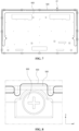
- FIG. 7 is a plan view schematically illustrating a combined structure of the cover bottom and the support main of the liquid crystal display device of the embodiment of the present disclosure
- FIG. 8 is an enlarged plan view of the area A1 of FIG. 7
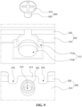
- FIG. 9 is an enlarged exploded perspective view of the area A1 of FIG. 7
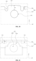
- FIG. 10 is an enlarged plan view of the cover bottom of the embodiment of the resent disclosure
- FIG. 11 is an enlarged plan view of the support main of the embodiment of the present disclosure.
- the areas indicated by the dotted line and including the area A1 represent screw-tightening parts.
- the support main 500 is disposed over the cover bottom 600. At this time, the support main 500 is disposed along the edges of the cover bottom 600.
- the support main 500 and the cover bottom 600 are combined with each other by a plurality of screws 800.
- the number and position of the plurality of screws 800 are not limited as illustrated and may vary.
- the cover bottom 600 includes the first cover portion 610 and the second cover portion 620, and the first cover portion 612 has the cover hole 612 with the press-fit nut 700 for tightening the screw 800 and the protrusion 614 corresponding to the cover hole 612.
- the cover hole 612 may not be provided in advance and may be formed in the process of applying the press-fit nut 700.
- the protrusion 614 protrudes outward from the outer surface of the second cover portion 620.
- the protrusion 614 also protrudes outward from the outer surface of the support main 500.
- the distance d3 from the cover hole 612 to the edge of the protrusion 614 in the X direction is greater than the X direction length d4 of the second cover portion 620.
- the protrusion 614 is disposed between the adjacent second cover portions 620 in the Y direction. Accordingly, each second cover portion 620 is disposed between the adjacent protrusions 614 in the Y direction.
- the protrusion 614 and the second cover portion 620 are spaced apart from each other, and the cover groove 616 is provided between the protrusion 614 and the second cover portion 620.
- the cover groove 616 may facilitate bending of the second cover portion 620.
- the support main 500 includes the first support portion 510 and the second support portion 520, the first support portion 510 has the support hole 512 for tightening the screw 800, and the support hole 512 has the first hoe portion 512a and the second hole portion 512b.
- the screw head 810 is disposed in the first hole portion 512a, and the screw body 820 is disposed in the second hole portion 512b.
- the screw body 820 is also disposed in the cover hole 612.
- first support portion 510 has the first support groove 514 in the outer surface thereof under the second support portion 520, and the second cover portion 620 is disposed in the first support groove 514.
- the X direction length d5 of the first support groove 514 may be equal to or greater than the X direction length d4 of the second cover portion 620.
- the protrusion 614 is disposed between the adjacent first support grooves 514 in the Y direction. Accordingly, the first support groove 514 is disposed between the adjacent protrusions 614 in the Y direction.
- the repair and reassembly can be facilitated when defects occur or problems occur.
- the screw-tightening position is moved as much as possible to the outside, so that the width of the bezel can be minimized.
Landscapes
- Physics & Mathematics (AREA)
- Nonlinear Science (AREA)
- Mathematical Physics (AREA)
- Chemical & Material Sciences (AREA)
- Crystallography & Structural Chemistry (AREA)
- General Physics & Mathematics (AREA)
- Optics & Photonics (AREA)
- Liquid Crystal (AREA)
Abstract
Description
- The present application claims priority of
KR Patent Application No. 10-2021-0189358 filed on December 28, 2021 - The present disclosure relates to a display device, and more particularly, to a liquid crystal display device having a narrow bezel.
- As the information society is in progress, a demand for display devices of displaying images increases in various forms, and flat panel display devices (FPD) such as liquid crystal display devices (LCD) and organic light emitting diode display devices (OLED) have been developed and applied to various fields.
- Among the flat panel display devices, liquid crystal display devices have been widely used because of their compact size, light weight, thin thickness, low power driving, and the like.
- The liquid crystal display devices use optical anisotropy and dielectric anisotropy of liquid crystal and include two substrates, a liquid crystal layer between the two substrates, and a pixel electrode and a common electrode for driving liquid crystal molecules of the liquid crystal layer. The liquid crystal display devices control the arrangement of the liquid crystal molecules by an electric field generated by applying a voltage to the pixel electrode and the common electrode and display images by the light transmittance changed accordingly. The liquid crystal display devices have been widely applied to portable devices such as cellphones or multimedia devices, monitors for notebooks or computers, and large televisions.
- In the liquid crystal display devices, an area except for a display area where an image is displayed becomes a bezel of products using the liquid crystal display devices. Recently, by minimizing a width of the bezel such that the display area is maximized in the display device having the same size, borderless products have been researched and developed with a neat appearance in which mechanical parts such as various cases or covers are not shown.
- To do this, structures have been suggested in which an adhesive member is used between components of the liquid crystal display device, and the adhesive member fixes the components by a strong adhesive force.
- However, when adhesion failure occurs or the components need to be repaired, it is difficult to separate the components because of the strong adhesive force of the adhesive member. Accordingly, in the process of separating the components, damages are applied to a liquid crystal panel or optical sheets of a backlight unit, so that repair and reassembly are difficult.
- Accordingly, the present disclosure is directed to a liquid crystal display device that substantially obviates one or more of the problems due to limitations and disadvantages described above. to a liquid crystal display device with a minimized bezel.
- More specifically, it is an object to provide a liquid crystal display device with a minimized bezel.
- It is also an object to provide a liquid crystal display device that can be easily repaired and reassembled.
- Additional features and aspects will be set forth in the description that follows, and in part will be apparent from the description, or may be learned by practice of the present disclosure provided herein. Other features and aspects of the inventive concepts may be realized and attained by the structure particularly pointed out in the written description, or derivable therefrom, and the claims hereof as well as the appended drawings.
- The object is solved by the features of the independent claims. Preferred embodiments are given in the dependent claims.
- To achieve these and other aspects of the present disclosure, as embodied and broadly described herein, a liquid crystal display device includes a cover bottom including a first cover portion of a first direction and a second cover portion of a second direction; a backlight unit over the cover bottom and including a light source, a diffusion plate, and an optical sheet; a support main maintaining a distance between the light source and the diffusion plate and including a first support portion and a second support portion; and a liquid crystal panel over the backlight unit and the support main, wherein the support main and the cover bottom are combined with each other by a plurality of screws, and wherein the first cover portion includes a plurality of protrusions protruding outward from an outer surface of the second cover portion and corresponding to the plurality of screws, respectively.
- In one more embodiments, The support main may be also called support main structure.
- In one more embodiments, the second cover portion may disposed between adjacent protrusions.
- In one more embodiments, the first cover portion may have a cover groove between the second cover portion and one of the plurality of protrusions.
- In one more embodiments, the first support portion may have a first support groove corresponding to the second cover portion.
- In one more embodiments, each protrusion may be disposed between adjacent first support grooves.
- In one more embodiments the first support portion may further have a second support groove corresponding to an edge of the light source.
- In one more embodiments the plurality of protrusions may protrude outward from an outer surface of the second support portion.
- In one more embodiments, the liquid crystal display device may further comprise a guide panel between the backlight unit and the liquid crystal panel.
- In one more embodiments, the guide panel may include a first guide portion extending in the first direction and a second guide portion extending in the second direction.
- In one more embodiments the plurality of protrusions may partially overlap the second guide portion.
- In one more embodiments, the first cover portion may have a cover hole corresponding to each screw.
- In one more embodiments, the first support portion may have a support hole corresponding to the cover hole.
- In one more embodiments, a press-fit nut may be is provided in the cover hole and the support hole.
- In one more embodiments the support hole may have a first hole part and a second hole part.
- In one more embodiments an area of the first hole part may be larger than an area of the second hole part.
- In one more embodiments, an inner side of the first hole part may be is opened.
- It is to be understood that both the foregoing general description and the following detailed description are exemplary and explanatory and are intended to provide further explanation of the inventive concepts as claimed.
- The accompanying drawings, which are included to provide a further understanding of the present disclosure and which are incorporated in and constitute a part of this application, illustrate aspects of the disclosure and together with the description serve to explain various principles of the present disclosure.
- In the drawings:
-
FIG. 1 is a schematic cross-sectional view of a LCD device of an embodiment of the disclosure; -
FIG. 2 is a schematic cross-sectional view of another part of the LCD device of the embodiment of the present disclosure; -
FIG. 3 is a top perspective view of the LCD device of the embodiment of the present disclosure; -
FIG. 4 is a bottom perspective view of the LCD device of the embodiment of the present disclosure; -
FIG. 5 is a top perspective view schematically showing a configuration between a cover bottom and a support main of the liquid crystal display device of the embodiment of the present disclosure; -
FIG. 6 is a bottom perspective view schematically showing the configuration between the cover bottom and the support main of the LCD device of the embodiment of the disclosure; -
FIG. 7 is a plan view schematically illustrating a combined structure of the cover bottom and the support main of the liquid crystal display device of the embodiment of the present disclosure; -
FIG. 8 is an enlarged plan view of the area A1 ofFIG. 7 ; -
FIG. 9 is an enlarged exploded perspective view of the area A1 ofFIG. 7 ; -
FIG. 10 is an enlarged plan view of the cover bottom of the embodiment of the resent disclosure; -
FIG. 11 is an enlarged plan view of the support main of the embodiment of the present disclosure. - Reference will now be made in detail to aspects of the disclosure, an exemplary embodiment of which is illustrated in the accompanying drawings.
-
FIG. 1 and FIG. 2 are schematic cross-sectional views of a LCD device of an embodiment of the present disclosure,FIG. 3 is a top perspective view of the LCD device of the embodiment of the present disclosure, andFIG. 4 is a bottom perspective view of the liquid crystal display device of the embodiment of the present disclosure. Here,FIGS. 1 ,3, and 4 show a part with a screw joint structure, andFIG. 2 shows a part without a screw joint structure. - Further,
FIG. 5 and FIG. 6 are a top perspective view and a bottom perspective view schematically showing a configuration between a cover bottom and a support main of the liquid crystal display device of the embodiment of the present disclosure, respectively, and show the part with the screw joint structure. - As shown in
FIGS. 1 to 6 , the liquid crystal display device of the embodiment of the present disclosure includes aliquid crystal panel 100, abacklight unit 200, anadhesive member 300, aguide panel 400, a support main 500, and acover bottom 600. The support main 500 and thecover bottom 600 are combined with each other by ascrew 800. The support main 500 may be also called supportmain structure 500. - The
liquid crystal panel 100 includes afirst substrate 110 in a lower position and asecond substrate 120 in an upper position, and a liquid crystal layer (not shown) is interposed between the first andsecond substrates - Although not shown in the figures, the
first substrate 110 includes a plurality of gate lines and a plurality of data lines on an inner surface thereof. The gate lines and the data lines cross each other to define a plurality of pixel regions. In each pixel region, a thin film transistor, a pixel electrode, and a common electrode are provided. The thin film transistor is connected to the corresponding gate line and the corresponding data line, and the pixel electrode is connected to the thin film transistor. The pixel electrode and the common electrode generate an electric field to drive liquid crystal molecules of the liquid crystal layer. Thisfirst substrate 110 may be referred to as an array substrate. - In addition, although not shown in the figures, the
second substrate 120 includes a black matrix, a color filter layer, and an overcoat layer on an inner surface thereof. The color filter layer includes red, green, and blue color filters, and the black matrix has openings corresponding to respective pixel regions. The red, green, and blue color filters of the color filter layer are disposed to correspond to the opening, respectively. Thissecond substrate 120 may be referred to as a color filter substrate. - A
side sealing member 150 is provided at side or lateral surfaces of the first andsecond substrates side sealing member 150 may be formed of a material absorbing light. - The
side sealing member 150 can prevent light leakage occurring at side surfaces of theliquid crystal panel 100. More specifically, some of light outputted from theliquid crystal panel 100 travel toward the side surfaces of theliquid crystal panel 100. Theside sealing member 150 is provided at the side surfaces of theliquid crystal panel 100, thereby blocking the light leakage due to the light traveling toward the side surfaces of theliquid crystal panel 100. - In addition, the
side sealing member 150 protects the side surfaces of theliquid crystal panel 100 from external impacts. - The
liquid crystal panel 100 further includes afirst polarizer 130 and asecond polarizer 140. Thefirst polarizer 130 is attached to an outer surface of thefirst substrate 110, that is, a lower surface of thefirst substrate 110, and thesecond polarizer 140 is attached to an outer surface of thesecond substrate 120, that is, an upper surface of thesecond substrate 120 in the context of the figures. - In the figures, the
first polarizer 130 is disposed under thefirst substrate 110, and thesecond polarizer 140 is disposed over thesecond substrate 120. Thefirst polarizer 130 and thesecond polarizer 140 transmit linearly-polarized light only parallel to respective transmission axes. The transmission axis of thefirst polarizer 130 is perpendicular to the transmission axis of thesecond polarizer 140. - One of the first and
second polarizer - Here, a size of the
second polarizer 140 is larger than a size of thefirst polarizer 130. Accordingly, thefirst polarizer 130 may be spaced apart from theside sealing member 150, and thesecond polarizer 140 may be in contact with theside sealing member 150. - Further, the size of the
first polarizer 130 is smaller than a size of thefirst substrate 110, and the outer surface of thefirst substrate 110 is partially exposed. More specifically, the outer surface of thefirst substrate 110 is exposed between an edge of thefirst polarizer 130 and an edge of thefirst substrate 110. - The
backlight unit 200 is disposed under theliquid crystal panel 100 to provide light to theliquid crystal panel 100. Thebacklight unit 200 includes a light emitting diode (LED)array 210, areflection plate 220, adiffusion plate 230, and anoptical sheet 240. - The
backlight unit 200 is a direct type in which theLED array 210 of a light source is disposed right under theliquid crystal panel 100. - The
LED array 210 may include a plurality ofLEDs 212. The LEDs might be provided on a printed circuit board (PCB). Here, eachLED 212 may be a mini LED having a size of 100 to 200 µm. Accordingly, by implementing the local dimming in which light is selectively provided to theliquid crystal panel 100 by zones, the black luminance is improved, so that the contrast ratio can be increased and the power consumption can be decreased. However, the present disclosure is not limited thereto, and various sizes and types of LEDs can be applied. - The
reflection plate 220 is provided on theLED array 210. Thereflection plate 220 has openings corresponding to theLEDs 212, and theLEDs 212 are arranged in the respective openings. Accordingly, light from theLEDs 212 travels toward theliquid crystal panel 100, and light reflected by theliquid crystal panel 100 or other components over theLEDs 212 and traveling toward thereflection plate 220 is reflected by thereflection plate 220 again and then is sent back to theliquid crystal panel 100, thereby increasing the light efficiency. - The
diffusion plate 230 is disposed over thereflection plate 220. Thediffusion plate 230 is spaced apart from theLED array 210 and thereflection plate 220 with a predetermined distance and uniformly diffuses light from theLEDs 212. The distance between thereflection plate 220 and thediffusion plate 230 is larger than the distance betweenoptical sheet 240 and thelower polarizer 130. - The
optical sheet 240 is disposed over thediffusion plate 230. Theoptical sheet 240 may include at least one diffusion sheet and at least one light-concentrating sheet such that more uniform surface light source can be incident on theliquid crystal panel 100 by diffusion or concentrating light passing through thediffusion plate 230. - For example, the
optical sheet 240 may include two light-concentrating sheets and one diffusion sheet sequentially disposed over thediffusion plate 230. The light-concentrating sheets may include prism patterns or lenticular patterns. In this case, one of the light-concentrating sheets may include lenticular patterns, and the other may include prism patterns. - Meanwhile, the
optical sheet 240 may further include a brightness enhancement film in which layers having different refractive indexes are alternately stacked or may the brightness enhancement film instead of the diffusion sheet. - The
liquid crystal panel 100 and thebacklight unit 200 are fastened and supported by theguide panel 400, the support main 500, and thecover bottom 600. - First, the
liquid crystal panel 100 is fastened on theguide panel 400. Theguide panel 400 may be formed along edges of theliquid crystal panel 100, thereby having a plane structure of a substantially square or rectangular frame shape. - The
guide panel 400 includes afirst guide portion 410 and asecond guide portion 420. Thefirst guide portion 410 may be a horizontal portion extending in an X direction, and thesecond guide portion 420 may be a vertical portion extending in a Z direction. One side end of thefirst guide portion 410 may be connected to an upper end of thesecond guide portion 420, and theguide panel 400 may have a substantially L- shaped cross-section. Meanwhile, the other side end of thefirst guide 410 may protrude toward the Z direction. That is, thefirst guide 410 may have a protrusion on at the other side end. - The
adhesive member 300 is proved between thefirst guide portion 410 of theguide panel 400 and theliquid crystal panel 100, in particular the edge of theliquid crystal panel 100, so that theliquid crystal panel 100 may be fixed to thefirst guide portion 410 by theadhesive member 300. - In this case, the
adhesive member 300 overlaps and contacts the exposed lower surface of thefirst substrate 110 and also overlaps and contacts at least partly thefirst polarizer 130. Theadhesive member 300 may be a foam pad having a cushioned property, and thus, theadhesive member 300 may act as a buffer absorbing external impacts. Theadhesive member 300 may be formed of an elastic material and for example, formed of polyethylene, polyacryl, or polyurethane. However, the present disclosure is not limited thereto. - The support main 500 is disposed under the
guide panel 400. The support main 500 may be formed along the edges of theliquid crystal panel 100, thereby having a plane structure of a substantially square or rectangular frame shape. The support main 500 includes afirst support portion 510 and asecond support portion 520. - The
first support portion 510 is disposed between thereflection plate 220 and thediffusion plate 230. Thesecond support portion 520 extends from an upper surface of an edge of thefirst support portion 510 toward the Z direction and surrounds side surfaces of thediffusion plate 230 and theoptical sheet 240. Thesecond support portion 520 is disposed between the side surfaces of thediffusion plate 230 and theoptical sheet 240 and thesecond guide portion 420 of theguide panel 400. - The
first support portion 510 maintains a certain distance between theLED array 210 and thediffusion plate 230 so that light from theLEDs 212 may be mixed to implement uniform surface light source. - The
diffusion plate 230 is disposed on thefirst support portion 510. Accordingly, thediffusion plate 230 and theoptical sheet 240 are disposed between thefirst support portion 510 and thefirst guide portion 410, and the upper surface of thefirst support portion 510 is in contact with a lower surface of thediffusion plate 230, thereby supporting thediffusion plate 230 and theoptical sheet 240. - An outer surface of the
first support portion 510 is adjacent to thesecond guide portion 420 of theguide panel 400 and is surrounded by thesecond guide portion 420. An inner surface of thefirst support portion 520 has an inclination. That is, thefirst support portion 510 has aninclined surface 510a on the inner side. Theinclined surface 510a reflects light from theLEDs 212 and sends the reflected light to thediffusion plate 230. - In addition, the
first support portion 510 has asupport hole 512, afirst support groove 514, and asecond support groove 516. - The
support hole 512 is provided to correspond to thescrew 800. Thesupport hole 512 includes afirst hole part 512a in which ascrew head 810 is disposed and asecond hole part 512b in which ascrew body 820 is disposed. An area of thefirst hole part 512a is larger than an area of thesecond hole part 512b on a planar view. At this time, thefirst hole part 512a is extended into theinclined surface 510a and its inner side is opened. Thesupport hole 512 is substantially provided in the inner surface and the upper surface of thefirst support portion 510. - The
first support groove 514 is provided in the outer surface of thefirst support portion 510 and is disposed under thesecond support portion 520. Thefirst support groove 514 is provided in a portion where thescrew 800 is not disposed. That is, thefirst support groove 514 is spaced apart from thesupport hole 512 and is provided in thefirst support portion 510. Asecond cover portion 620 of thecover bottom 600 is disposed in thefirst support groove 514. - The
second support groove 516 is provided on a lower side of theinclined surface 510a of thefirst support portion 510. Edges of theLED array 210 and thereflection plate 220 are disposed in thesecond support groove 516, and thefirst support portion 510 presses and fastens the edges of theLED array 210 and thereflection plate 220, thereby preventing them from being separated. Accordingly, it is not necessary to provide an additional structure for preventing the separation of thereflection plate 220. - The support main 500 may be formed of plastic and/or may be molded. For example, the support main 500 may be formed of white polycarbonate (PC), but is not limited thereto.
- The
cover bottom 600 is provided under the support main 500. Thecover bottom 600 includes afirst cover portion 610 and thesecond cover portion 620. Thefirst cover portion 610 is a horizontal plane and extends substantially in the X direction. Thefirst cover potion 610 may have at least one bent part to displace various components necessary for driving theliquid crystal panel 100. - The
second cover portion 620 is a vertical plane and extends in the Z direction. Thesecond cover portion 620 is bended from thefirst cover portion 610. Thesecond cover portion 620 is disposed in thefirst support groove 514 of the support main 500. Accordingly, thesecond cover portion 620 is disposed between thesecond guide portion 420 of theguide panel 400 and thefirst support portion 510 of the support main 500 to thereby prevent the support main 500 from being pushed outward. As described above, thecover bottom 600 is combined with the support main 500 through thescrew 800. To do this, thefirst cover portion 610 of thecover bottom 600 has acover hole 612. Thecover hole 612 is disposed under thesupport hole 512. - Meanwhile, the
cover bottom 600 has aprotrusion 614 to correspond to thecover hole 612, and acover groove 616 is provided between theprotrusion 614 and thesecond cover portion 620. This will be described in detail later. - A press-
fit nut 700, which is commonly referred to as a PEM nut, is provided in thecover hole 612. The press-fit nut 700 is also disposed in thesecond hole portion 512b of thesupport hole 512. However, the present disclosure is not limited thereto. Alternatively, a screw thread may be formed in thecover hole 612 by a tapping method instead of the press-fit nut 700. - The press-
fit nut 700 is engaged with thescrew 800, so that thecover bottom 600 is combined with the support main 500. In this case, thescrew body 820 is disposed inside the press-fit nut 700. - Meanwhile, an
adhesive tape 900 is attached to an outer surface of thesecond guide portion 420 of theguide panel 400 and a lower surface of thefirst cover portion 610 of thecover bottom 600 to fix theguide panel 400 and thecover bottom 600. - In the liquid crystal display device of the embodiment of the present disclosure, the width of the bezel can be reduced. This will be described with reference to
FIG. 1 . - In
FIG. 1 , when an embedded screw is applied, a first distance d1 corresponding to the width of the bezel depends on a second distance d2 from the outer surface of theguide panel 400 to a bottom end of theinclined surface 510a of the support main 500. At this time, the second distance d2 is determined according to the type ofscrew 800 and a location of thecover hole 612 corresponding thereto. Further, in order to prevent separation thereflection plate 220, it is additionally necessary to maintain a certain distance between thereflection plate 220 and the support main 500. Accordingly, when the embedded screw is applied, the second distance d2 is increased - On the other hand, when an opened screw is applied, the second distance d2 can be decreased as compared to the embedded screw because a wall enclosing the screw is not needed.
- Meanwhile, the second distance d2 can be reduced as the location of the
cover hole 612 corresponding to thescrew 800 is closer to the outer surface of theguide panel 400. In this case, in order to apply the press-fit nut 700 or form the screw thread by the tapping method, a third distance d3 that is a minimum interval from the edge of thefirst cover portion 610 is required. For example, the third distance d3 may be 1.5 mm, but is not limited thereto. - Accordingly, in the liquid crystal display device of the embodiment of the present disclosure, the
protrusion 614 is provided in thefirst cover portion 610 to correspond to thecover hole 612 so that the location of thecover hole 612 is close to the outer surface of theguide panel 400. - An edge of the
protrusion 614 is disposed outside outer surfaces of thesecond cover portion 620 and the support main 500, and theprotrusion 614 overlaps thesecond guide portion 420 of theguide panel 400 along the Z direction. At this time, the edge of theprotrusion 614 is disposed inside the outer surface of thesecond guide portion 420. - As described above, in the liquid crystal display device of the embodiment of the present disclosure, the support main 500 and the
cover bottom 600 are engaged by thescrew 800, so that repair and rework can be facilitated when defects or problems occur. - In addition, since the opened screw is applied and the
protrusion 614 is provided in thesecond cover portion 620 of thecover bottom 600, the tightening position of thescrew 800 can be moved as much as possible to theguide panel 400, so that the second distance d2 can be decreased and the width d1 of the bezel can be minimized. For example, the width d1 of the bezel may be 4 mm or less, beneficially, 3 mm or less. - In this case, a white screw may be used or white paint may be applied to the
screw head 810 so that the openedscrew 800 is not visibly recognized to the outside. - A detailed structure of the cover bottom and the support main of the liquid crystal display device of the embodiment of the present disclosure will be described in detail with reference to
FIGS. 7 to 11 . -
FIG. 7 is a plan view schematically illustrating a combined structure of the cover bottom and the support main of the liquid crystal display device of the embodiment of the present disclosure, -
FIG. 8 is an enlarged plan view of the area A1 ofFIG. 7 ,FIG. 9 is an enlarged exploded perspective view of the area A1 ofFIG. 7 ,FIG. 10 is an enlarged plan view of the cover bottom of the embodiment of the resent disclosure, andFIG. 11 is an enlarged plan view of the support main of the embodiment of the present disclosure. InFIG. 7 , the areas indicated by the dotted line and including the area A1 represent screw-tightening parts. - In
FIGS. 7 to 11 , the support main 500 is disposed over thecover bottom 600. At this time, the support main 500 is disposed along the edges of thecover bottom 600. - The support main 500 and the
cover bottom 600 are combined with each other by a plurality ofscrews 800. The number and position of the plurality ofscrews 800 are not limited as illustrated and may vary. - The
cover bottom 600 includes thefirst cover portion 610 and thesecond cover portion 620, and thefirst cover portion 612 has thecover hole 612 with the press-fit nut 700 for tightening thescrew 800 and theprotrusion 614 corresponding to thecover hole 612. - Here, the
cover hole 612 may not be provided in advance and may be formed in the process of applying the press-fit nut 700. - The
protrusion 614 protrudes outward from the outer surface of thesecond cover portion 620. In addition, theprotrusion 614 also protrudes outward from the outer surface of the support main 500. In this case, the distance d3 from thecover hole 612 to the edge of theprotrusion 614 in the X direction is greater than the X direction length d4 of thesecond cover portion 620. - The
protrusion 614 is disposed between the adjacentsecond cover portions 620 in the Y direction. Accordingly, eachsecond cover portion 620 is disposed between theadjacent protrusions 614 in the Y direction. - The
protrusion 614 and thesecond cover portion 620 are spaced apart from each other, and thecover groove 616 is provided between theprotrusion 614 and thesecond cover portion 620. Thecover groove 616 may facilitate bending of thesecond cover portion 620. - Meanwhile, the support main 500 includes the
first support portion 510 and thesecond support portion 520, thefirst support portion 510 has thesupport hole 512 for tightening thescrew 800, and thesupport hole 512 has thefirst hoe portion 512a and thesecond hole portion 512b. - The
screw head 810 is disposed in thefirst hole portion 512a, and thescrew body 820 is disposed in thesecond hole portion 512b. Thescrew body 820 is also disposed in thecover hole 612. - In addition, the
first support portion 510 has thefirst support groove 514 in the outer surface thereof under thesecond support portion 520, and thesecond cover portion 620 is disposed in thefirst support groove 514. The X direction length d5 of thefirst support groove 514 may be equal to or greater than the X direction length d4 of thesecond cover portion 620. - As described above, since the
second cover portion 620 is disposed in thefirst support groove 514, theprotrusion 614 is disposed between the adjacentfirst support grooves 514 in the Y direction. Accordingly, thefirst support groove 514 is disposed between theadjacent protrusions 614 in the Y direction. - In the present disclosure, since the support main and the cover bottom are combined with each other by the screws, the repair and reassembly can be facilitated when defects occur or problems occur.
- Additionally, in the present disclosure, by providing the protrusion, the screw-tightening position is moved as much as possible to the outside, so that the width of the bezel can be minimized.
- Further, since it is not necessary to provide an additional structure for preventing the separation of the reflection plate, costs can be reduced.
- It will be apparent to those skilled in the art that various modifications and variations can be made in the display device of the present disclosure without departing from the technical idea or scope of the disclosure. Thus, it is intended that the present disclosure cover the modifications and variations of this disclosure provided they come within the scope of the appended claims and their equivalents.
Claims (11)
- A liquid crystal display device, comprising:a cover bottom (600) including a first cover portion (610) extending in a first direction (X) and a second cover portion (620) extending in a second direction; (Z) a backlight unit (200) disposed over the cover bottom (600) and including a light source (212), a diffusion plate (230), and an optical sheet (240);a support main (500) maintaining a distance between the light source (212) and the diffusion plate (230) and including a first support portion (510) and a second support portion (520); anda liquid crystal panel (100) disposed over the backlight unit (200) and the support main (500),wherein the support main (500) and the cover bottom (600) are combined with each other by a plurality of screws (820), andwherein the first cover portion (610) includes a plurality of protrusions (614) protruding outward from an outer surface of the second cover portion (620) and corresponding to the plurality of screws (820), respectively.
- The liquid crystal display device of claim 1, wherein the second cover portion (620) is disposed between adjacent protrusions (614).
- The liquid crystal display device of claim 1 or 2, wherein the first cover portion (610) has a cover groove (616) between the second cover portion (620) and one of the plurality of protrusions (614).
- The liquid crystal display device of any one of claims 1, 2 or 3, wherein the first support portion (510) has a first support groove (514) corresponding to the second cover portion (620).
- The liquid crystal display device of claim 4, wherein each protrusion (614) is disposed between adjacent first support grooves (514).
- The liquid crystal display device of claim 4 or 5, wherein the first support portion (510) further has a second support groove (516) corresponding to an edge of the light source (212).
- The liquid crystal display device of any one of the preceding claims, wherein the plurality of protrusions (514) protrude outward from an outer surface of the second support portion (520).
- The liquid crystal display device of any one of the preceding claims, further comprising a guide panel (400) between the backlight unit (200) and the liquid crystal panel (100).
- The liquid crystal display device of claim 8, wherein the guide panel (400) includes a first guide portion (410) extending in the first direction (X) and a second guide portion (420) extending in the second direction (Z), and/or
wherein the plurality of protrusions (514) partially overlap the second guide portion (420). - The liquid crystal display device of any one of the preceding claims, wherein the first cover portion (610) has a cover hole (612) corresponding to each screw (820) and the first support portion (510) has a support hole (512) corresponding to the cover hole (612), and/or
a press-fit nut (700) is provided in the cover hole (612) and the support hole (512). - The liquid crystal display device of claim 10, wherein the support hole (512) has a first hole part (512a) and a second hole part (512b), and/or
wherein an area of the first hole part (512a) is larger than an area of the second hole part (512b), and/or an inner side of the first hole part (512a) is opened.
Applications Claiming Priority (1)
| Application Number | Priority Date | Filing Date | Title |
|---|---|---|---|
| KR1020210189358A KR102902675B1 (en) | 2021-12-28 | 2021-12-28 | Liquid Crystal Display Device |
Publications (2)
| Publication Number | Publication Date |
|---|---|
| EP4206803A1 true EP4206803A1 (en) | 2023-07-05 |
| EP4206803B1 EP4206803B1 (en) | 2025-01-01 |
Family
ID=84359285
Family Applications (1)
| Application Number | Title | Priority Date | Filing Date |
|---|---|---|---|
| EP22208124.2A Active EP4206803B1 (en) | 2021-12-28 | 2022-11-17 | Liquid crystal display device |
Country Status (4)
| Country | Link |
|---|---|
| US (1) | US12235532B2 (en) |
| EP (1) | EP4206803B1 (en) |
| KR (1) | KR102902675B1 (en) |
| CN (1) | CN116360138B (en) |
Citations (3)
| Publication number | Priority date | Publication date | Assignee | Title |
|---|---|---|---|---|
| US20130070475A1 (en) * | 2011-09-15 | 2013-03-21 | Lg Display Co., Ltd. | Backlight unit for liquid crystal display device |
| KR20190056519A (en) * | 2017-11-17 | 2019-05-27 | 엘지디스플레이 주식회사 | Liquid crystal display device |
| KR20210049578A (en) * | 2019-10-25 | 2021-05-06 | 삼성전자주식회사 | Display apparatus |
Family Cites Families (15)
| Publication number | Priority date | Publication date | Assignee | Title |
|---|---|---|---|---|
| KR100619582B1 (en) * | 1999-10-08 | 2006-09-01 | 삼성전자주식회사 | Liquid crystal display module, liquid crystal display device employing the same, and assembly method thereof |
| KR100918280B1 (en) * | 2003-02-17 | 2009-09-18 | 엘지디스플레이 주식회사 | LCD Display Module |
| KR101107690B1 (en) * | 2004-12-24 | 2012-01-25 | 엘지디스플레이 주식회사 | Liquid crystal display module |
| KR101203520B1 (en) * | 2005-10-29 | 2012-11-23 | 엘지디스플레이 주식회사 | Assembling structure of liquid crystal display |
| KR20080057780A (en) * | 2006-12-21 | 2008-06-25 | 엘지디스플레이 주식회사 | Liquid crystal display module |
| KR20080109518A (en) | 2007-06-13 | 2008-12-17 | 엘지디스플레이 주식회사 | LCD Display |
| JP5149419B2 (en) * | 2011-04-27 | 2013-02-20 | シャープ株式会社 | Thin display device |
| KR101854852B1 (en) * | 2011-10-28 | 2018-06-14 | 엘지이노텍 주식회사 | Lighting apparatus |
| KR101898588B1 (en) | 2011-11-04 | 2018-09-13 | 엘지전자 주식회사 | Display apparatus |
| KR102227615B1 (en) * | 2014-11-24 | 2021-03-16 | 엘지디스플레이 주식회사 | Liquid crystal display device |
| US9826667B2 (en) * | 2015-04-27 | 2017-11-21 | Lg Display Co., Ltd. | Display device |
| KR20170125514A (en) * | 2016-05-04 | 2017-11-15 | 엘지디스플레이 주식회사 | Liquid Crystal Display Device |
| CN112305810B (en) * | 2019-07-26 | 2024-08-06 | 京东方科技集团股份有限公司 | Backlight module, display device and assembly method of display device |
| KR102652075B1 (en) * | 2019-12-30 | 2024-03-27 | 엘지디스플레이 주식회사 | Liquid crystal display device |
| KR20210100232A (en) * | 2020-02-05 | 2021-08-17 | 희성전자 주식회사 | Case member for liquid crystal module and lipuidcrystal display |
-
2021
- 2021-12-28 KR KR1020210189358A patent/KR102902675B1/en active Active
-
2022
- 2022-10-08 CN CN202211224389.9A patent/CN116360138B/en active Active
- 2022-10-19 US US17/969,649 patent/US12235532B2/en active Active
- 2022-11-17 EP EP22208124.2A patent/EP4206803B1/en active Active
Patent Citations (3)
| Publication number | Priority date | Publication date | Assignee | Title |
|---|---|---|---|---|
| US20130070475A1 (en) * | 2011-09-15 | 2013-03-21 | Lg Display Co., Ltd. | Backlight unit for liquid crystal display device |
| KR20190056519A (en) * | 2017-11-17 | 2019-05-27 | 엘지디스플레이 주식회사 | Liquid crystal display device |
| KR20210049578A (en) * | 2019-10-25 | 2021-05-06 | 삼성전자주식회사 | Display apparatus |
Also Published As
| Publication number | Publication date |
|---|---|
| KR102902675B1 (en) | 2025-12-19 |
| US12235532B2 (en) | 2025-02-25 |
| CN116360138B (en) | 2025-09-12 |
| CN116360138A (en) | 2023-06-30 |
| EP4206803B1 (en) | 2025-01-01 |
| KR20230099915A (en) | 2023-07-05 |
| US20230204994A1 (en) | 2023-06-29 |
Similar Documents
| Publication | Publication Date | Title |
|---|---|---|
| US8860904B2 (en) | Chassis having interlocking assembly parts and display device having the same | |
| US7708451B2 (en) | Bottom frame for liquid crystal display device, backlight assembly and liquid crystal display device using the same | |
| US9366893B2 (en) | Liquid crystal display device | |
| US7312838B2 (en) | Liquid crystal display device comprising a protecting unit for enclosing a fastener and holding lamp wires | |
| US8441597B2 (en) | Liquid crystal display device for preventing light leakage | |
| KR20120068499A (en) | Backlight unit and liquid crystal display device and method having the same | |
| US20110157518A1 (en) | Light shaping film and liquid crystal display device including the same | |
| US20130077343A1 (en) | Backlight unit and display apparatus having the same | |
| US7559683B2 (en) | Backlight assembly, light guiding plate including plurality of discontinuously formed prisms | |
| US7695178B2 (en) | Light-guide plate, backlight assembly and liquid crystal display having the same | |
| US20070153155A1 (en) | Liquid crystal display and method of manufacturing the same | |
| CN1603905A (en) | Liquid crystal display device | |
| KR20120116290A (en) | Liquid crystal display device | |
| US7826005B2 (en) | Light source supporting member, display device comprising the same and method thereof | |
| KR20120057388A (en) | Backlight unit and liquid crystal display device and method having the same | |
| EP4206803B1 (en) | Liquid crystal display device | |
| KR20120075135A (en) | Light shielding tape and backlight unit using the same and liquid crystal display device having thereof | |
| KR20120067205A (en) | Backlight unit, liquid crystal display device and method assembling thereof | |
| KR102328942B1 (en) | Backlight unit and display device including the same | |
| KR20150037299A (en) | Liquid crystal display device | |
| KR101981587B1 (en) | Liquid crystal display device | |
| KR20150049280A (en) | Liquid crystal display device and method for fabricating the same | |
| KR101277219B1 (en) | Flat panel display device | |
| US20240168331A1 (en) | Liquid crystal display device | |
| KR20130037293A (en) | Back light unit and liguid crystal display module using the same |
Legal Events
| Date | Code | Title | Description |
|---|---|---|---|
| PUAI | Public reference made under article 153(3) epc to a published international application that has entered the european phase |
Free format text: ORIGINAL CODE: 0009012 |
|
| STAA | Information on the status of an ep patent application or granted ep patent |
Free format text: STATUS: THE APPLICATION HAS BEEN PUBLISHED |
|
| AK | Designated contracting states |
Kind code of ref document: A1 Designated state(s): AL AT BE BG CH CY CZ DE DK EE ES FI FR GB GR HR HU IE IS IT LI LT LU LV MC ME MK MT NL NO PL PT RO RS SE SI SK SM TR |
|
| STAA | Information on the status of an ep patent application or granted ep patent |
Free format text: STATUS: REQUEST FOR EXAMINATION WAS MADE |
|
| 17P | Request for examination filed |
Effective date: 20240104 |
|
| RBV | Designated contracting states (corrected) |
Designated state(s): AL AT BE BG CH CY CZ DE DK EE ES FI FR GB GR HR HU IE IS IT LI LT LU LV MC ME MK MT NL NO PL PT RO RS SE SI SK SM TR |
|
| GRAP | Despatch of communication of intention to grant a patent |
Free format text: ORIGINAL CODE: EPIDOSNIGR1 |
|
| STAA | Information on the status of an ep patent application or granted ep patent |
Free format text: STATUS: GRANT OF PATENT IS INTENDED |
|
| RIC1 | Information provided on ipc code assigned before grant |
Ipc: G02F 1/1333 20060101AFI20240605BHEP |
|
| INTG | Intention to grant announced |
Effective date: 20240624 |
|
| GRAS | Grant fee paid |
Free format text: ORIGINAL CODE: EPIDOSNIGR3 |
|
| GRAA | (expected) grant |
Free format text: ORIGINAL CODE: 0009210 |
|
| STAA | Information on the status of an ep patent application or granted ep patent |
Free format text: STATUS: THE PATENT HAS BEEN GRANTED |
|
| AK | Designated contracting states |
Kind code of ref document: B1 Designated state(s): AL AT BE BG CH CY CZ DE DK EE ES FI FR GB GR HR HU IE IS IT LI LT LU LV MC ME MK MT NL NO PL PT RO RS SE SI SK SM TR |
|
| REG | Reference to a national code |
Ref country code: GB Ref legal event code: FG4D |
|
| REG | Reference to a national code |
Ref country code: CH Ref legal event code: EP |
|
| REG | Reference to a national code |
Ref country code: DE Ref legal event code: R096 Ref document number: 602022009314 Country of ref document: DE |
|
| REG | Reference to a national code |
Ref country code: IE Ref legal event code: FG4D |
|
| REG | Reference to a national code |
Ref country code: LT Ref legal event code: MG9D |
|
| REG | Reference to a national code |
Ref country code: NL Ref legal event code: MP Effective date: 20250101 |
|
| REG | Reference to a national code |
Ref country code: AT Ref legal event code: MK05 Ref document number: 1756847 Country of ref document: AT Kind code of ref document: T Effective date: 20250101 |
|
| PG25 | Lapsed in a contracting state [announced via postgrant information from national office to epo] |
Ref country code: NL Free format text: LAPSE BECAUSE OF FAILURE TO SUBMIT A TRANSLATION OF THE DESCRIPTION OR TO PAY THE FEE WITHIN THE PRESCRIBED TIME-LIMIT Effective date: 20250101 |
|
| PG25 | Lapsed in a contracting state [announced via postgrant information from national office to epo] |
Ref country code: FI Free format text: LAPSE BECAUSE OF FAILURE TO SUBMIT A TRANSLATION OF THE DESCRIPTION OR TO PAY THE FEE WITHIN THE PRESCRIBED TIME-LIMIT Effective date: 20250101 |
|
| PG25 | Lapsed in a contracting state [announced via postgrant information from national office to epo] |
Ref country code: PL Free format text: LAPSE BECAUSE OF FAILURE TO SUBMIT A TRANSLATION OF THE DESCRIPTION OR TO PAY THE FEE WITHIN THE PRESCRIBED TIME-LIMIT Effective date: 20250101 |
|
| PG25 | Lapsed in a contracting state [announced via postgrant information from national office to epo] |
Ref country code: ES Free format text: LAPSE BECAUSE OF FAILURE TO SUBMIT A TRANSLATION OF THE DESCRIPTION OR TO PAY THE FEE WITHIN THE PRESCRIBED TIME-LIMIT Effective date: 20250101 |
|
| PG25 | Lapsed in a contracting state [announced via postgrant information from national office to epo] |
Ref country code: IS Free format text: LAPSE BECAUSE OF FAILURE TO SUBMIT A TRANSLATION OF THE DESCRIPTION OR TO PAY THE FEE WITHIN THE PRESCRIBED TIME-LIMIT Effective date: 20250501 Ref country code: NO Free format text: LAPSE BECAUSE OF FAILURE TO SUBMIT A TRANSLATION OF THE DESCRIPTION OR TO PAY THE FEE WITHIN THE PRESCRIBED TIME-LIMIT Effective date: 20250401 |
|
| PG25 | Lapsed in a contracting state [announced via postgrant information from national office to epo] |
Ref country code: HR Free format text: LAPSE BECAUSE OF FAILURE TO SUBMIT A TRANSLATION OF THE DESCRIPTION OR TO PAY THE FEE WITHIN THE PRESCRIBED TIME-LIMIT Effective date: 20250101 |
|
| PG25 | Lapsed in a contracting state [announced via postgrant information from national office to epo] |
Ref country code: LV Free format text: LAPSE BECAUSE OF FAILURE TO SUBMIT A TRANSLATION OF THE DESCRIPTION OR TO PAY THE FEE WITHIN THE PRESCRIBED TIME-LIMIT Effective date: 20250101 Ref country code: PT Free format text: LAPSE BECAUSE OF FAILURE TO SUBMIT A TRANSLATION OF THE DESCRIPTION OR TO PAY THE FEE WITHIN THE PRESCRIBED TIME-LIMIT Effective date: 20250502 |
|
| PG25 | Lapsed in a contracting state [announced via postgrant information from national office to epo] |
Ref country code: BG Free format text: LAPSE BECAUSE OF FAILURE TO SUBMIT A TRANSLATION OF THE DESCRIPTION OR TO PAY THE FEE WITHIN THE PRESCRIBED TIME-LIMIT Effective date: 20250101 Ref country code: GR Free format text: LAPSE BECAUSE OF FAILURE TO SUBMIT A TRANSLATION OF THE DESCRIPTION OR TO PAY THE FEE WITHIN THE PRESCRIBED TIME-LIMIT Effective date: 20250402 |
|
| PG25 | Lapsed in a contracting state [announced via postgrant information from national office to epo] |
Ref country code: AT Free format text: LAPSE BECAUSE OF FAILURE TO SUBMIT A TRANSLATION OF THE DESCRIPTION OR TO PAY THE FEE WITHIN THE PRESCRIBED TIME-LIMIT Effective date: 20250101 |
|
| PG25 | Lapsed in a contracting state [announced via postgrant information from national office to epo] |
Ref country code: CZ Free format text: LAPSE BECAUSE OF FAILURE TO SUBMIT A TRANSLATION OF THE DESCRIPTION OR TO PAY THE FEE WITHIN THE PRESCRIBED TIME-LIMIT Effective date: 20250101 |
|
| PG25 | Lapsed in a contracting state [announced via postgrant information from national office to epo] |
Ref country code: SE Free format text: LAPSE BECAUSE OF FAILURE TO SUBMIT A TRANSLATION OF THE DESCRIPTION OR TO PAY THE FEE WITHIN THE PRESCRIBED TIME-LIMIT Effective date: 20250101 |
|
| REG | Reference to a national code |
Ref country code: DE Ref legal event code: R097 Ref document number: 602022009314 Country of ref document: DE |
|
| PG25 | Lapsed in a contracting state [announced via postgrant information from national office to epo] |
Ref country code: SM Free format text: LAPSE BECAUSE OF FAILURE TO SUBMIT A TRANSLATION OF THE DESCRIPTION OR TO PAY THE FEE WITHIN THE PRESCRIBED TIME-LIMIT Effective date: 20250101 |
|
| PG25 | Lapsed in a contracting state [announced via postgrant information from national office to epo] |
Ref country code: DK Free format text: LAPSE BECAUSE OF FAILURE TO SUBMIT A TRANSLATION OF THE DESCRIPTION OR TO PAY THE FEE WITHIN THE PRESCRIBED TIME-LIMIT Effective date: 20250101 |
|
| PG25 | Lapsed in a contracting state [announced via postgrant information from national office to epo] |
Ref country code: IT Free format text: LAPSE BECAUSE OF FAILURE TO SUBMIT A TRANSLATION OF THE DESCRIPTION OR TO PAY THE FEE WITHIN THE PRESCRIBED TIME-LIMIT Effective date: 20250101 |
|
| PGFP | Annual fee paid to national office [announced via postgrant information from national office to epo] |
Ref country code: FR Payment date: 20250925 Year of fee payment: 4 |
|
| PG25 | Lapsed in a contracting state [announced via postgrant information from national office to epo] |
Ref country code: EE Free format text: LAPSE BECAUSE OF FAILURE TO SUBMIT A TRANSLATION OF THE DESCRIPTION OR TO PAY THE FEE WITHIN THE PRESCRIBED TIME-LIMIT Effective date: 20250101 |
|
| PG25 | Lapsed in a contracting state [announced via postgrant information from national office to epo] |
Ref country code: RO Free format text: LAPSE BECAUSE OF FAILURE TO SUBMIT A TRANSLATION OF THE DESCRIPTION OR TO PAY THE FEE WITHIN THE PRESCRIBED TIME-LIMIT Effective date: 20250101 |
|
| PG25 | Lapsed in a contracting state [announced via postgrant information from national office to epo] |
Ref country code: SK Free format text: LAPSE BECAUSE OF FAILURE TO SUBMIT A TRANSLATION OF THE DESCRIPTION OR TO PAY THE FEE WITHIN THE PRESCRIBED TIME-LIMIT Effective date: 20250101 |
|
| PLBE | No opposition filed within time limit |
Free format text: ORIGINAL CODE: 0009261 |
|
| STAA | Information on the status of an ep patent application or granted ep patent |
Free format text: STATUS: NO OPPOSITION FILED WITHIN TIME LIMIT |
|
| 26N | No opposition filed |
Effective date: 20251002 |
|
| PGFP | Annual fee paid to national office [announced via postgrant information from national office to epo] |
Ref country code: DE Payment date: 20250922 Year of fee payment: 4 |