EP4206786B1 - Imaging light path and head-mounted display device - Google Patents
Imaging light path and head-mounted display device Download PDFInfo
- Publication number
- EP4206786B1 EP4206786B1 EP21909103.0A EP21909103A EP4206786B1 EP 4206786 B1 EP4206786 B1 EP 4206786B1 EP 21909103 A EP21909103 A EP 21909103A EP 4206786 B1 EP4206786 B1 EP 4206786B1
- Authority
- EP
- European Patent Office
- Prior art keywords
- lens
- imaging light
- glued
- light path
- light ray
- Prior art date
- Legal status (The legal status is an assumption and is not a legal conclusion. Google has not performed a legal analysis and makes no representation as to the accuracy of the status listed.)
- Active
Links
Images





Classifications
-
- G—PHYSICS
- G02—OPTICS
- G02B—OPTICAL ELEMENTS, SYSTEMS OR APPARATUS
- G02B27/00—Optical systems or apparatus not provided for by any of the groups G02B1/00 - G02B26/00, G02B30/00
- G02B27/01—Head-up displays
- G02B27/017—Head mounted
- G02B27/0172—Head mounted characterised by optical features
-
- G—PHYSICS
- G02—OPTICS
- G02B—OPTICAL ELEMENTS, SYSTEMS OR APPARATUS
- G02B27/00—Optical systems or apparatus not provided for by any of the groups G02B1/00 - G02B26/00, G02B30/00
- G02B27/28—Optical systems or apparatus not provided for by any of the groups G02B1/00 - G02B26/00, G02B30/00 for polarising
- G02B27/283—Optical systems or apparatus not provided for by any of the groups G02B1/00 - G02B26/00, G02B30/00 for polarising used for beam splitting or combining
Definitions
- the present disclosure relates to the technical field of near-eye display, in particular to an imaging light path and a head mounted display.
- the imaging system In the current virtual reality equipment, light rays from the display screen are usually transmitted and amplified by the imaging system and then transmitted to the human eye. In order to achieve image amplification, the imaging system usually needs a combination of multiple lenses.
- CN212111989U discloses an imaging light path comprising two lenses connected together by a glue layer.
- the imaging light path comprises:
- a surface of the first lens facing away from the display screen is a second surface, and the quarter wave plate is provided on the second surface; a surface of the second lens facing the first lens is a third surface, the glued film layer further comprises a polarizing film, the polarizing film is provided on the third surface, and the reflective polarizing film is provided on a side of the polarizing film facing the first lens.
- a surface of the second lens facing away from the first lens is a fourth surface, and at least one of the second surface, the third surface and the fourth surface is provided thereon with an anti-reflection film.
- At least one of the first surface and the fourth surface is an aspherical surface.
- the second surface and the third surface have a same shape.
- the second surface and the third surface are flat surfaces, a focal power of the first lens is defined as ⁇ 1 and satisfies 0 ⁇ ⁇ 1 ⁇ 0.06, a focal power of the second lens is defined as ⁇ 2 and satisfies -0.01 ⁇ ⁇ 2 ⁇ 0, a thickness of the first lens is defined as T1 and satisfies 2.0 mm ⁇ T1 ⁇ 8.0 mm, a thickness of the second lens is defined as T2 and satisfies 2.0 mm ⁇ T2 ⁇ 5.0 mm, and the imaging light path has an optical distortion less than 30%, a chromatic aberration less than 70 ⁇ m and an angle of view greater than 90°.
- the second surface and the third surface are aspherical surfaces, the second surface and the third surface bulge toward the display screen, a focal power of the first lens is defined as ⁇ 3 and satisfies 0 ⁇ ⁇ 3 ⁇ 0.1, a focal power of the second lens is defined as ⁇ 4 and satisfies 0 ⁇ ⁇ 4 ⁇ 0.005, a thickness of the first lens is defined as T3 and satisfies 2.0 mm ⁇ T3 ⁇ 5.0 mm, a thickness of the second lens is defined as T4 and satisfies 2.0 mm ⁇ T4 ⁇ 8.0 mm, and the imaging light path has a chromatic aberration less than 190 ⁇ m and an angle of view greater than 100°.
- the glued film layer further comprises a glued layer, and the glued layer is disposed between the quarter wave plate and the reflective polarizing film.
- the imaging light path further comprises a calibration assembly, wherein the calibration assembly is connected to the glued lens group and configured to adjust a distance between the glued lens group and the display screen.
- the present disclosure also provides a head mounted display.
- the head mounted display comprises a housing and an imaging light path as described above, and the imaging light path is disposed in the housing.
- the display screen emits the imaging light ray.
- the imaging light ray passes through the glued lens group.
- the glued lens group comprises the first lens and the second lens, and the imaging light ray passes through the first lens and the second lens successively.
- the first surface of the first lens is provided thereon with a semi-reflective and semi-transmissive film, and a glued film layer is provided between the first lens and the second lens.
- the glued film layer comprises the quarter wave plate and the reflective polarizing film.
- the imaging light ray passing through the semi-reflective and semi-transmissive film passes through the first lens.
- the imaging light ray enters the quarter wave plate.
- the polarization state of the imaging light ray changes from circular polarization to linear polarization.
- the imaging light ray in the linear polarization state enters the reflective polarizing film.
- the polarization transmission direction of the reflective polarizing film is different from the polarization direction of the imaging light ray in the linear polarization state, and the imaging light ray cannot pass through the reflective polarizing film and is reflected back to the quarter wave plate by the reflective polarizing film.
- the linear polarization state changes back to the circular polarization state again, and then it travels toward the semi-reflective and semi-transmissive film.
- the imaging light ray is reflected and transmitted again on the surface of the semi-reflective and semi-transmissive film. Part of the imaging light ray is reflected and travels to the quarter wave plate again, and the imaging light ray in the linearly polarized state is generated again.
- the polarization angle of the imaging light ray in the linearly polarized state changes. At this point, the polarization direction of the imaging light ray is the same as that of the polarization reflective film, and the imaging light ray passes through the polarization reflective film, and form an image at the position of a user's eyes.
- the imaging for display is mainly conducted by the glued lens group, and the first lens and the second lens are glued together without an air gap formed therebetween, so the dust in the external environment is difficult to enter between the first lens and the second lens.
- the dust is difficult to deposit on the surface of the first lens or the second lens, thereby ensuring the smooth passage of the imaging light ray, reducing the impact of the dust on the imaging system, avoiding the loss of the formed image, and making the formed image brighter.
- display screen 110, imaging light ray; 20, glued lens group; 210, first lens; 211, first surface; 212, second surface; 220, second lens; 221, third surface; 222 fourth surface; 30, glued film layer; 310, quarter wave plate; 320, glued layer; 330, reflective polarizing film; 340, polarizing film; 40, protection plate.
- first and second are used for descriptive purposes only and are not to be construed as indicating or implying relative importance or implicitly indicating the number of indicated technical features.
- a feature with “first” or “second” may explicitly or implicitly include at least one such a feature.
- a plurality of means at least two, such as two, three, etc., unless expressly defined otherwise.
- the terms "connected”, “fixed” and the like should be understood in a broad sense, for example, it may be fixedly connected, or removably connected, or integrally connected; it may also be mechanically connected or electrically connected; it may also be directly connected or indirectly connected through a middleware; it may also be internally communicated or interacted between two components.
- the specific meaning of these terms in the present disclosure should be understood according to specific situations.
- Multiple lenses in the imaging system that realize the light path transmission are designed to be separate. There are gaps between lenses.
- the dust in the external environment is deposited on the surface of the lens, and will affect the smooth passage of light rays, which will result in the loss of the formed image of the imaging system or the low brightness of the formed image.
- the present disclosure provides an imaging light path, which can be applied to a head mounted display.
- a head mounted display There are many kinds of display principles of the head mounted display, such as VR (Virtual Reality) display principle and AR (Augmented Reality) display principle.
- the imaging light path comprises: a display screen 10 and a glued lens group 20.
- the display screen 10 emits an imaging light ray 110.
- the glued lens group 20 is disposed in an exit direction of the imaging light ray 110, and is configured to complete the amplification and transmission of the image formed on the display screen 10.
- the lenses in the glued lens group 20 are glued together with little or no spacing or gap between them, so it is difficult for outside dust to enter the glued lens group 20.
- the glued lens group 20 comprises a first lens 210 and a second lens 220 that are arranged successively along the propagation direction of the imaging light ray 110.
- first lens 210 and the second lens 220 are also glued together, and it is difficult for outside dust to enter between the first lens 210 and the second lens 220.
- the surface of the first lens 210 facing the display screen 10 is the first surface 211, and the first surface 211 bulges toward the display screen 10.
- the image formed on the display screen 10 needs to be amplified and transmitted.
- the imaging light ray will diverge after being emitted from the display screen, and the convex setting of the first surface 211 can play the role of converging the imaging light ray 110, so that the imaging light ray can effectively converge to the human eye.
- the first surface 211 is provided thereon with a semi-reflective and semi-transmissive film, and a glued film layer 30 is provided between the first lens 210 and the second lens 220.
- the glued film layer 30 comprises a quarter wave plate 310 and a reflective polarizing film 330 arranged successively along the propagation direction of the imaging light ray 110.
- the quarter wave plate 310 can convert the polarization state of the imaging light ray 110, for example, convert a linearly polarized light ray to a circularly polarized light ray or visa versa.
- the reflective polarizing film 330 has a polarization transmission direction. When the imaging light ray 110 vibrates along the polarization transmission direction, it can pass through the reflective polarizing film 330 smoothly. When the imaging light ray 110 vibrating in other directions reaches the reflective polarizing film 330, it will be reflected.
- the reflective polarizing film 330 and the quarter wave plate 310 may be provided by plating or by gluing. The gluing method is easier to operate, while the plating method can fix more firmly.
- the light exit surface of the display screen 10 is also provided with a protective plate 40, which may be transparent glass or transparent plastic.
- the protective plate 40 is mainly used to protect the display screen 10 and prevent the light exit surface of the display screen 10 from being damaged by external forces.
- the display screen 10 emits the imaging light ray 110.
- the imaging light ray 110 passes through the glued lens group 20.
- the glued lens group 20 comprises the first lens 210 and the second lens 220, and the imaging light ray 110 passes through the first lens 210 and the second lens 220 successively.
- the first surface 211 of the first lens 210 is provided thereon with a semi-reflective and semi-transmissive film, and a glued film layer 30 is provided between the first lens 210 and the second lens 220.
- the glued film layer 30 comprises the quarter wave plate 310 and the reflective polarizing film 330.
- the imaging light ray 110 After the imaging light ray 110 is emitted from the display screen 10, when the imaging light ray 110 passes through the semi-reflective and semi-transmissive film, part of the imaging light ray 110 is reflected and part of the imaging light ray 110 is transmitted.
- the imaging light ray 110 passing through the semi-reflective and semi-transmissive film passes through the first lens 210.
- the imaging light ray 110 enters the quarter wave plate 310. Under the action of the quarter wave plate 310, the polarization state of the imaging light ray 110 changes from circular polarization to linear polarization.
- the imaging light ray 110 in the linear polarization state enters the reflective polarizing film 330.
- the polarization transmission direction of the reflective polarizing film 330 is different from the polarization direction of the imaging light ray 110 in the linear polarization state, and the imaging light ray 110 cannot pass through the reflective polarizing film 330 and is reflected back to the quarter wave plate 310 by the reflective polarizing film 330.
- the linear polarization state changes back to the circular polarization state again, and then it travels toward the semi-reflective and semi-transmissive film.
- the imaging light ray 110 is reflected and transmitted again on the surface of the semi-reflective and semi-transmissive film.
- the imaging light ray 110 is reflected and travels to the quarter wave plate 310 again, and the imaging light ray 110 in the linearly polarized state is generated again. After two times of reflection, the polarization angle of the imaging light ray 110 in the linearly polarized state changes. At this point, the polarization direction of the imaging light ray 110 is the same as that of the polarization reflective film 330, and the imaging light ray 110 passes through the polarization reflective film 330, and form an image at the position of a user's eyes.
- the imaging for display is mainly conducted by the glued lens group 20, and the first lens 210 and the second lens 220 are glued together without an air gap formed therebetween, so the dust in the external environment is difficult to enter between the first lens 210 and the second lens 220.
- the dust is difficult to deposit on the surface of the first lens 210 or the second lens 220, thereby ensuring the smooth passage of the imaging light ray 110, reducing the impact of the dust on the imaging system, avoiding the loss of the formed image, and making the formed image brighter.
- the imaging light ray 110 when they are vertical to each other, the imaging light ray 110 is reflected. Besides these two cases, there may be a case that they form an angle ranging from 0° to 90°. Namely, the polarization direction of the imaging light ray 110 and the polarization transmission direction of the reflective polarizing film 330 are in a state between same and vertical. In this case, part of light ray will be transmitted through the reflective polarizing film 330, and thus stray light will appear.
- the surface of the first lens 210 facing away from the display screen 10 is defined as the second surface 212, and the quarter wave plate 310 is provided on the second surface 212; the surface of the second lens 220 facing the first lens 210 is defined as the third surface 221, and the glued film layer 30 further comprises a polarizing film 340 provided on the third surface 221, and the reflective polarizing film 330 is provided on the side of the polarizing film 340 facing the first lens 210. It can be seen from this that the imaging light ray 110 travels toward the polarizing film 340 after passing through the polarizing reflection film 330.
- the polarizing film 340 is also called a polarizer or polarizing plate, and can eliminate stray light, and thus can ensure the imaging quality of the imaging light ray 110.
- the polarizing film 340 can be provided on the third surface 221 by plating or by gluing. The gluing method is easier to operate, while the plating method can make the film layer firmer.
- the imaging light ray 110 is easy to lose when it is propagated in the air or the lens, resulting in a decrease in the brightness of the formed image.
- the surface of the second lens 220 facing away from the first lens 210 is defined as the fourth surface 222, and at least one of the second surface 212, the third surface 221, and the fourth surface 222 is provided thereon with an anti-reflection film.
- the transmission quantity of the imaging light ray 110 can be increased and the light loss can be reduced.
- the second surface 212, the third surface 221, and the fourth surface 222 may be all provided with anti-reflection films.
- the anti-reflection film may be provided on one of the second surface 212, the third surface 221 and the fourth surface 222, which can reduce the processing cost while improving the light transmission quantity.
- At least one of the first surface 211 and the fourth surface 222 is an aspherical surface. Aspheric surfaces can effectively eliminate aberration.
- the first surface 211 and the fourth surface 222 may both be aspherical surfaces, or one of them is an aspherical surface.
- first surface 211 and the fourth surface 222 may also be free curved surfaces, and the aberration formed by the imaging light ray 110 can also be eliminated by the free curved surfaces.
- the second surface 212 and the third surface 221 have the same shape.
- the first lens 210 and the second lens 220 are glued together, and the second surface 212 and the third surface 221 are surfaces butting against each other. If they have the same shape, when they are butted and glued, the gap between them can be reduced, and thus they can be butted and glued more compactly.
- the second surface 212 and the third surface 221 are flat surfaces
- the focal power of the first lens 210 is defined as ⁇ 1 and satisfies 0 ⁇ ⁇ 1 ⁇ 0.06
- the focal power of the second lens 220 is defined as ⁇ 2 and satisfies -0.01 ⁇ ⁇ 2 ⁇
- the thickness of the first lens 210 is defined as T1 and satisfies 2.0 mm ⁇ T1 ⁇ 8.0 mm
- the thickness of the second lens 220 is defined as T2 and satisfies 2.0 mm ⁇ T2 ⁇ 5.0 mm
- the imaging light path has an optical distortion less than 30%, a chromatic aberration less than 70 ⁇ m and an angle of view greater than 90°.
- the thickness of the first lens 210 refers to the distance from the first surface 211 to the second surface 212 at the center point position of the first lens 210; the thickness of the second lens 220 refers to the distance from the third surface 221 to the fourth surface 222 at the center point position of the second lens 220.
- Table 1 surface type radius thickness material conic constant A4 A6 fourth surface even order aspheric surface -433.569 2.159 OKP1 0 3.935E-05 -1.815E-06 first surface even order aspheric surface -52.571 -7.9
- z is a coordinate along the optical axis
- Y is a radial coordinate in the unit of lens length
- C is the curvature (1/R)
- k is the conic constant
- ⁇ i is the coefficient of each higher-order term
- 2i is the order of aspheric coefficient.
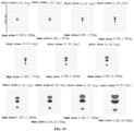
- the spot diagram of this embodiment refers to that, after the light ray emitted from a point passes through the image display structure, due to aberration, its intersection points with the image plane is no longer converged at the same point but scattered in a certain range. It is used to evaluate the image quality of the image display structure. Areas 1 to 10 are arranged from left to right and from top to bottom. It can be seen that the image height corresponding to the maximum half field of view is less than 11.892 mm.
- FIG. 7 shows the modulation transfer function curve (i.e., MTF chart) of this embodiment.
- the MTF diagram refers to the relationship between the modulation degree and the line pairs per millimeter in the image, and is used to evaluate the restoration ability of the scene details.
- the uppermost black solid line is a curve without aberration in theory, and the closer to the black solid line, the better the imaging quality will be.
- the curves in FIG. 7 are scattered, most curves are close to the black solid line, which meets the design specifications.
- Fig. 8 shows the distortion diagram in this embodiment.
- Distortion refers to that when the object is imaged by the image display structure, different parts of the object have aberrations with different magnification. Distortion will lead to reduced similarity between the object and the image, but will not affect the resolution of the image. It can be seen from FIG. 8 that the optical distortion at the maximum field of view is viarable in the range of less than 30%, and the distortion is small, which meets the design requirements.
- FIG. 9 shows the lateral chromatic aberration diagram in this embodiment.
- the lateral chromatic aberration also known as the chromatic difference of magnification, mainly refers to that a polychromatic main ray of the object side becomes multiple rays when exiting from the image side due to the dispersion of the refraction system. It can be seen that the maximum position of the field of view with maximum dispersion is less than 70 ⁇ m, which can meet the needs of end users later on.
- the second surface 212 and the third surface 221 are aspherical surfaces, and the second surface 212 and the third surface 221 bulge toward the display screen 10.
- the focal power of the first lens is defined as ⁇ 3 and satisfies 0 ⁇ ⁇ 3 ⁇ 0.1
- the focal power of the second lens is defined as ⁇ 4 and satisfies 0 ⁇ ⁇ 4 ⁇ 0.005
- the thickness of the first lens is defined as T3 and satisfies 2.0 mm ⁇ T3 ⁇ 5.0 mm
- the thickness of the second lens is defined as T4 and satisfies 2.0 mm ⁇ T4 ⁇ 8.0 mm
- the imaging light path has a chromatic aberration less than 190 ⁇ m and an angle of view greater than 100°.
- the second surface 212 and the third surface 221 are aspherical, which can further eliminate the imaging aberration.
- the thickness of the first lens 210 refers to the distance from the first surface 211 to the second surface 212 at the center point position of the first lens 210; the thickness of the second lens 220 refers to the distance from the third surface 221 to the fourth surface 222 at the center point position of the second lens 220.
- Table 2 surface type radius thickness material conic constant A4 A6 fourth surface even order aspheric surface -155 3.4209 APL50 13VH 0 1.813E-05 -6.805E-08 second surface even order aspheric surface -80 0 0 0 0 first surface even order aspheric surface -46.716 -8.009 APL50 13VH -0.81494 2.152E-06 9.155E-10
- z is a coordinate along the optical axis
- Y is a radial coordinate in the unit of lens length
- C is the curvature (1/R)
- k is the conic constant
- ⁇ i is the coefficient of each higher-order term
- 2i is the order of aspheric coefficient.
- the spot diagram of this embodiment refers to that, after the light ray emitted from a point passes through the image display structure, due to aberration, its intersection points with the image plane is no longer converged at the same point but scattered in a certain range. It is used to evaluate the image quality of the image display structure. Areas 1 to 11 are arranged from left to right and from top to bottom. It can be seen that the image height corresponding to the maximum half field of view is less than 18.988 mm.
- FIG. 11 shows the modulation transfer function curve (i.e., MTF chart) of this embodiment.
- the MTF diagram refers to the relationship between the modulation degree and the line pairs per millimeter in the image, and is used to evaluate the restoration ability of the scene details.
- the uppermost black solid line is a curve without aberration in theory, and the closer to the black solid line, the better the imaging quality will be.
- the curves in FIG. 11 are scattered, most curves are close to the black solid line, which meets the design specifications.
- FIG. 13 shows the lateral chromatic aberration diagram in this embodiment.
- the lateral chromatic aberration also known as the chromatic difference of magnification, mainly refers to that a polychromatic main ray of the object side becomes multiple rays when exiting from the image side due to the dispersion of the refraction system. It can be seen that the maximum position of the field of view with maximum dispersion is less than 190 ⁇ m, which can meet the needs of end users later on.
- the glued film layer 30 further comprises a glued layer 320, which is disposed between the quarter wave plate 310 and the reflective polarizing film 330.
- the glued layer 320 is sticky, and the quarter wave plate 310 and the polarizing reflection film 330 can be glued together by the glued layer 320.
- the imaging light path comprises a calibration assembly.
- the calibration assembly is connected to the glued lens group 20, and is configured to adjust the distance between the glued lens group 20 and the display screen 10.
- the calibration assembly can drive the glued lens group 20 to move close to or far from the display screen 10.
- the imaging position of the imaging light path can be changed by adjusting the distance between the glued lens group 20 and the display screen 10.
- the imaging light path can be applied to myopia or hyperopia.
- the imaging light path can be adjusted within the range of 0° to 800° myopia.
- the present disclosure also provides a head mounted display.
- the head mounted display comprises a housing and an imaging light path as described above, and the imaging light path is provided in the housing. If the imaging light path is provided in the housing, the housing can effectively protect the imaging light path, prevent dust from falling into the imaging light path, and also reduce water infiltration into the imaging light path to avoid imaging light path failure.
- the specific embodiments of the head mounted display in the present disclosure may refer to the above embodiments of the imaging light path, and will not be repeated here.
Landscapes
- Physics & Mathematics (AREA)
- General Physics & Mathematics (AREA)
- Optics & Photonics (AREA)
- Lenses (AREA)
Description
- This application claims priority to
Chinese patent application No. 202011532252.0 filed with the China Patent Office on December 21, 2021 - The present disclosure relates to the technical field of near-eye display, in particular to an imaging light path and a head mounted display.
- In the current virtual reality equipment, light rays from the display screen are usually transmitted and amplified by the imaging system and then transmitted to the human eye. In order to achieve image amplification, the imaging system usually needs a combination of multiple lenses.
- Multiple lenses are designed to be separate. There are gaps between lenses. Dust in the external environment enters the imaging system via the gaps between lenses and is deposited on the surface of the lens. The deposited dust will affect the smooth passage of light rays, which will result in the loss of the formed image of the imaging system or the low brightness of the formed image.
CN212111989U discloses an imaging light path comprising two lenses connected together by a glue layer. - Thus, with respect to the problem that the deposited dust on the surface of the lens affects the smooth passage of light rays, and results in the loss of the formed image of the imaging system or the low brightness of the formed image, it is necessary to provide an imaging light path and a head mounted display, which can reduce dust deposition on the surface of the lens, so that the light can pass through the lens smoothly, thereby avoiding the loss of the formed image and ensuring the brightness of the formed image.
- To achieve the above object, an imaging light path proposed in the present disclosure. The imaging light path comprises:
- a display screen emitting an imaging light ray; and
- a glued lens group disposed in an exit direction of the imaging light ray;
- wherein the glued lens group comprises a first lens and a second lens arranged successively along a propagation direction of the imaging light ray;
- a surface of the first lens facing the display screen is a first surface, and the first surface bulges toward the display screen;
- the first surface is provided thereon with a semi-reflective and semi-transmissive film, a glued film layer is provided between the first lens and the second lens, and the glued film layer comprises a quarter wave plate and a reflective polarizing film arranged successively along the propagation direction of the imaging light ray.
- A surface of the first lens facing away from the display screen is a second surface, and the quarter wave plate is provided on the second surface;
a surface of the second lens facing the first lens is a third surface, the glued film layer further comprises a polarizing film, the polarizing film is provided on the third surface, and the reflective polarizing film is provided on a side of the polarizing film facing the first lens. - Optionally, a surface of the second lens facing away from the first lens is a fourth surface, and at least one of the second surface, the third surface and the fourth surface is provided thereon with an anti-reflection film.
- Optionally, at least one of the first surface and the fourth surface is an aspherical surface.
- The second surface and the third surface have a same shape.
- The second surface and the third surface are flat surfaces, a focal power of the first lens is defined as φ1 and satisfies 0 < φ1 < 0.06, a focal power of the second lens is defined as φ2 and satisfies -0.01< φ2 < 0, a thickness of the first lens is defined as T1 and satisfies 2.0 mm < T1 < 8.0 mm, a thickness of the second lens is defined as T2 and satisfies 2.0 mm < T2 < 5.0 mm, and the imaging light path has an optical distortion less than 30%, a chromatic aberration less than 70 µm and an angle of view greater than 90°.
- The second surface and the third surface are aspherical surfaces, the second surface and the third surface bulge toward the display screen, a focal power of the first lens is defined as φ3 and satisfies 0 < φ3 < 0.1, a focal power of the second lens is defined as φ4 and satisfies 0 < φ4 < 0.005, a thickness of the first lens is defined as T3 and satisfies 2.0 mm < T3 < 5.0 mm, a thickness of the second lens is defined as T4 and satisfies 2.0 mm < T4 < 8.0 mm, and the imaging light path has a chromatic aberration less than 190 µm and an angle of view greater than 100°.
- The glued film layer further comprises a glued layer, and the glued layer is disposed between the quarter wave plate and the reflective polarizing film.
- Optionally, the imaging light path further comprises a calibration assembly, wherein the calibration assembly is connected to the glued lens group and configured to adjust a distance between the glued lens group and the display screen.
- In addition, in order to achieve the above object, the present disclosure also provides a head mounted display. The head mounted display comprises a housing and an imaging light path as described above, and the imaging light path is disposed in the housing.
- In the technical solution proposed in the present disclosure, the display screen emits the imaging light ray. The imaging light ray passes through the glued lens group. The glued lens group comprises the first lens and the second lens, and the imaging light ray passes through the first lens and the second lens successively. The first surface of the first lens is provided thereon with a semi-reflective and semi-transmissive film, and a glued film layer is provided between the first lens and the second lens. The glued film layer comprises the quarter wave plate and the reflective polarizing film. After the imaging light ray is emitted from the display screen, when the imaging light ray passes through the semi-reflective and semi-transmissive film, part of the imaging light ray is reflected and part of the imaging light ray is transmitted. The imaging light ray passing through the semi-reflective and semi-transmissive film passes through the first lens. The imaging light ray enters the quarter wave plate. Under the action of the quarter wave plate, the polarization state of the imaging light ray changes from circular polarization to linear polarization. The imaging light ray in the linear polarization state enters the reflective polarizing film. At this point, the polarization transmission direction of the reflective polarizing film is different from the polarization direction of the imaging light ray in the linear polarization state, and the imaging light ray cannot pass through the reflective polarizing film and is reflected back to the quarter wave plate by the reflective polarizing film. After the imaging light ray passes through the quarter wave plate, the linear polarization state changes back to the circular polarization state again, and then it travels toward the semi-reflective and semi-transmissive film. The imaging light ray is reflected and transmitted again on the surface of the semi-reflective and semi-transmissive film. Part of the imaging light ray is reflected and travels to the quarter wave plate again, and the imaging light ray in the linearly polarized state is generated again. After two times of reflection, the polarization angle of the imaging light ray in the linearly polarized state changes. At this point, the polarization direction of the imaging light ray is the same as that of the polarization reflective film, and the imaging light ray passes through the polarization reflective film, and form an image at the position of a user's eyes.
- It can be seen that the imaging for display is mainly conducted by the glued lens group, and the first lens and the second lens are glued together without an air gap formed therebetween, so the dust in the external environment is difficult to enter between the first lens and the second lens. As a result, the dust is difficult to deposit on the surface of the first lens or the second lens, thereby ensuring the smooth passage of the imaging light ray, reducing the impact of the dust on the imaging system, avoiding the loss of the formed image, and making the formed image brighter.
- In order to more clearly illustrate the technical solutions in the embodiments of the present disclosure or the prior art, drawings necessary for describing the embodiments or the prior art will be briefly introduced below. Obviously, the drawings in the following description are only a part of the drawings of the present disclosure. For a person of ordinary skill in the art, other drawings can be obtained based on the drawings provided without paying creative efforts.
-
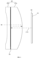
FIG. 1 is a schematic diagram of the structure of an embodiment of an imaging light path according to the present disclosure; -
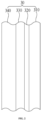
FIG. 2 is a schematic diagram of the structure of the glued film layer inFIG. 1 ; -
FIG. 3 is a schematic diagram of the structure of a first lens and a second lens inFIG. 1 ; -
FIG. 4 is a schematic diagram of the structure of another embodiment of an imaging light path according to the present disclosure; -
FIG. 5 is a schematic diagram of the structure of a first lens and a second lens inFIG. 4 ; -
FIG. 6 is a spot diagram of the imaging light path inFIG. 1 ; -
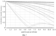
FIG. 7 is a modulation transfer function curve of the imaging light path inFIG. 1 ; -
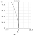
FIG. 8 is a distortion diagram of the imaging light path inFIG. 1 ; -
FIG. 9 is a lateral chromatic aberration diagram of the imaging light path inFIG. 1 ; -
FIG. 10 is a spot diagram of the imaging light path inFIG. 4 ; -
FIG. 11 is a modulation transfer function curve of the imaging light path inFIG. 4 ; -
FIG. 12 is a distortion diagram of the imaging light path inFIG. 4 ; and -
FIG. 13 is a lateral chromatic aberration diagram of the imaging light path inFIG. 4 . - In the drawings: 10, display screen; 110, imaging light ray; 20, glued lens group; 210, first lens; 211, first surface; 212, second surface; 220, second lens; 221, third surface; 222 fourth surface; 30, glued film layer; 310, quarter wave plate; 320, glued layer; 330, reflective polarizing film; 340, polarizing film; 40, protection plate.
- The realization of the object, functional features and advantages of the present disclosure will be further described in conjunction with embodiments with reference to the drawings.
- The technical solutions in embodiments of the present disclosure will be described clearly and completely below with reference to the drawings in the embodiments of the present disclosure. Obviously, the embodiments as described below are merely part of, rather than all, embodiments of the present disclosure. Based on the embodiments of the present disclosure, any other embodiment obtained by a person of ordinary skill in the art without paying any creative effort shall fall within the protection scope of the present disclosure.
- It should be noted that all directional indications (such as up, down, left, right, front, back, etc.) in the embodiments of the present disclosure are only used to explain the relative positional relationship, the movement situation, etc. among various components under a certain posture (as shown in the accompanying drawings). If the specific posture changes, the directional indication will also change accordingly.
- In addition, in the present disclosure, the terms "first" and "second" are used for descriptive purposes only and are not to be construed as indicating or implying relative importance or implicitly indicating the number of indicated technical features. Thus, a feature with "first" or "second" may explicitly or implicitly include at least one such a feature. In the description of the present disclosure, "a plurality of" means at least two, such as two, three, etc., unless expressly defined otherwise.
- In the present disclosure, unless otherwise expressly specified and defined, the terms "connected", "fixed" and the like should be understood in a broad sense, for example, it may be fixedly connected, or removably connected, or integrally connected; it may also be mechanically connected or electrically connected; it may also be directly connected or indirectly connected through a middleware; it may also be internally communicated or interacted between two components. For a person of ordinary skill in the art, the specific meaning of these terms in the present disclosure should be understood according to specific situations.
- In addition, the technical solutions in various embodiments of the present disclosure can be combined with each other if their combination is realizable to a person of ordinary skill in the art. When the combination of technical solutions is contradictory or cannot be realized, it should be considered that such a combination of technical solutions does not exist and is not within the scope of protection claimed in the present disclosure.
- Multiple lenses in the imaging system that realize the light path transmission are designed to be separate. There are gaps between lenses. The dust in the external environment is deposited on the surface of the lens, and will affect the smooth passage of light rays, which will result in the loss of the formed image of the imaging system or the low brightness of the formed image.
- In order to solve the above problem, as shown in
FIG. 1 , the present disclosure provides an imaging light path, which can be applied to a head mounted display. There are many kinds of display principles of the head mounted display, such as VR (Virtual Reality) display principle and AR (Augmented Reality) display principle. - The imaging light path comprises: a
display screen 10 and a gluedlens group 20. Thedisplay screen 10 emits animaging light ray 110. The gluedlens group 20 is disposed in an exit direction of theimaging light ray 110, and is configured to complete the amplification and transmission of the image formed on thedisplay screen 10. The lenses in the gluedlens group 20 are glued together with little or no spacing or gap between them, so it is difficult for outside dust to enter the gluedlens group 20. The gluedlens group 20 comprises afirst lens 210 and asecond lens 220 that are arranged successively along the propagation direction of theimaging light ray 110. It can be seen that thefirst lens 210 and thesecond lens 220 are also glued together, and it is difficult for outside dust to enter between thefirst lens 210 and thesecond lens 220. The surface of thefirst lens 210 facing thedisplay screen 10 is thefirst surface 211, and thefirst surface 211 bulges toward thedisplay screen 10. The image formed on thedisplay screen 10 needs to be amplified and transmitted. The imaging light ray will diverge after being emitted from the display screen, and the convex setting of thefirst surface 211 can play the role of converging theimaging light ray 110, so that the imaging light ray can effectively converge to the human eye. - The
first surface 211 is provided thereon with a semi-reflective and semi-transmissive film, and a gluedfilm layer 30 is provided between thefirst lens 210 and thesecond lens 220. The gluedfilm layer 30 comprises aquarter wave plate 310 and a reflectivepolarizing film 330 arranged successively along the propagation direction of theimaging light ray 110. When theimaging light ray 110 passes through the semi-reflective and semi-transmissive film, a part of the light ray reflects and the other part transmits. Thequarter wave plate 310 can convert the polarization state of theimaging light ray 110, for example, convert a linearly polarized light ray to a circularly polarized light ray or visa versa. The reflectivepolarizing film 330 has a polarization transmission direction. When theimaging light ray 110 vibrates along the polarization transmission direction, it can pass through the reflectivepolarizing film 330 smoothly. When theimaging light ray 110 vibrating in other directions reaches the reflectivepolarizing film 330, it will be reflected. The reflectivepolarizing film 330 and thequarter wave plate 310 may be provided by plating or by gluing. The gluing method is easier to operate, while the plating method can fix more firmly. - Further, the light exit surface of the
display screen 10 is also provided with aprotective plate 40, which may be transparent glass or transparent plastic. Theprotective plate 40 is mainly used to protect thedisplay screen 10 and prevent the light exit surface of thedisplay screen 10 from being damaged by external forces. - In the technical solution proposed in the present disclosure, the
display screen 10 emits theimaging light ray 110. Theimaging light ray 110 passes through the gluedlens group 20. The gluedlens group 20 comprises thefirst lens 210 and thesecond lens 220, and theimaging light ray 110 passes through thefirst lens 210 and thesecond lens 220 successively. Thefirst surface 211 of thefirst lens 210 is provided thereon with a semi-reflective and semi-transmissive film, and a gluedfilm layer 30 is provided between thefirst lens 210 and thesecond lens 220. The gluedfilm layer 30 comprises thequarter wave plate 310 and the reflectivepolarizing film 330. After theimaging light ray 110 is emitted from thedisplay screen 10, when theimaging light ray 110 passes through the semi-reflective and semi-transmissive film, part of theimaging light ray 110 is reflected and part of theimaging light ray 110 is transmitted. Theimaging light ray 110 passing through the semi-reflective and semi-transmissive film passes through thefirst lens 210. Theimaging light ray 110 enters thequarter wave plate 310. Under the action of thequarter wave plate 310, the polarization state of theimaging light ray 110 changes from circular polarization to linear polarization. Theimaging light ray 110 in the linear polarization state enters the reflectivepolarizing film 330. At this point, the polarization transmission direction of the reflectivepolarizing film 330 is different from the polarization direction of theimaging light ray 110 in the linear polarization state, and theimaging light ray 110 cannot pass through the reflectivepolarizing film 330 and is reflected back to thequarter wave plate 310 by the reflectivepolarizing film 330. After theimaging light ray 110 passes through thequarter wave plate 310, the linear polarization state changes back to the circular polarization state again, and then it travels toward the semi-reflective and semi-transmissive film. Theimaging light ray 110 is reflected and transmitted again on the surface of the semi-reflective and semi-transmissive film. Part of theimaging light ray 110 is reflected and travels to thequarter wave plate 310 again, and theimaging light ray 110 in the linearly polarized state is generated again. After two times of reflection, the polarization angle of theimaging light ray 110 in the linearly polarized state changes. At this point, the polarization direction of theimaging light ray 110 is the same as that of the polarizationreflective film 330, and theimaging light ray 110 passes through the polarizationreflective film 330, and form an image at the position of a user's eyes. - It can be seen that the imaging for display is mainly conducted by the glued
lens group 20, and thefirst lens 210 and thesecond lens 220 are glued together without an air gap formed therebetween, so the dust in the external environment is difficult to enter between thefirst lens 210 and thesecond lens 220. As a result, the dust is difficult to deposit on the surface of thefirst lens 210 or thesecond lens 220, thereby ensuring the smooth passage of theimaging light ray 110, reducing the impact of the dust on the imaging system, avoiding the loss of the formed image, and making the formed image brighter. - In the above embodiment, when the polarization direction of the
imaging light ray 110 and the polarization transmission direction of the reflectivepolarizing film 330 are the same, theimaging light ray 110 is transmitted; when they are vertical to each other, theimaging light ray 110 is reflected. Besides these two cases, there may be a case that they form an angle ranging from 0° to 90°. Namely, the polarization direction of theimaging light ray 110 and the polarization transmission direction of the reflectivepolarizing film 330 are in a state between same and vertical. In this case, part of light ray will be transmitted through the reflectivepolarizing film 330, and thus stray light will appear. To reduce stray light, the surface of thefirst lens 210 facing away from thedisplay screen 10 is defined as thesecond surface 212, and thequarter wave plate 310 is provided on thesecond surface 212; the surface of thesecond lens 220 facing thefirst lens 210 is defined as thethird surface 221, and the gluedfilm layer 30 further comprises apolarizing film 340 provided on thethird surface 221, and the reflectivepolarizing film 330 is provided on the side of thepolarizing film 340 facing thefirst lens 210. It can be seen from this that theimaging light ray 110 travels toward thepolarizing film 340 after passing through thepolarizing reflection film 330. Thepolarizing film 340 is also called a polarizer or polarizing plate, and can eliminate stray light, and thus can ensure the imaging quality of theimaging light ray 110. Thepolarizing film 340 can be provided on thethird surface 221 by plating or by gluing. The gluing method is easier to operate, while the plating method can make the film layer firmer. - In the above embodiment, the
imaging light ray 110 is easy to lose when it is propagated in the air or the lens, resulting in a decrease in the brightness of the formed image. For this reason, the surface of thesecond lens 220 facing away from thefirst lens 210 is defined as thefourth surface 222, and at least one of thesecond surface 212, thethird surface 221, and thefourth surface 222 is provided thereon with an anti-reflection film. By providing the anti-reflection film, the transmission quantity of theimaging light ray 110 can be increased and the light loss can be reduced. In order to maximize the amount of theimaging light ray 110 transmitted, thesecond surface 212, thethird surface 221, and thefourth surface 222 may be all provided with anti-reflection films. Alternatively, the anti-reflection film may be provided on one of thesecond surface 212, thethird surface 221 and thefourth surface 222, which can reduce the processing cost while improving the light transmission quantity. - In the above embodiment, when the
imaging ray 110 is reflected for many times, the aberration will be easy to generate. For this reason, at least one of thefirst surface 211 and thefourth surface 222 is an aspherical surface. Aspheric surfaces can effectively eliminate aberration. Thefirst surface 211 and thefourth surface 222 may both be aspherical surfaces, or one of them is an aspherical surface. - In addition, the
first surface 211 and thefourth surface 222 may also be free curved surfaces, and the aberration formed by theimaging light ray 110 can also be eliminated by the free curved surfaces. - In an embodiment of the present disclosure, the
second surface 212 and thethird surface 221 have the same shape. Thefirst lens 210 and thesecond lens 220 are glued together, and thesecond surface 212 and thethird surface 221 are surfaces butting against each other. If they have the same shape, when they are butted and glued, the gap between them can be reduced, and thus they can be butted and glued more compactly. - As shown in
FIG. 3 , in the above embodiment, thesecond surface 212 and thethird surface 221 are flat surfaces, the focal power of thefirst lens 210 is defined as φ1 and satisfies 0 < φ1 < 0.06, the focal power of thesecond lens 220 is defined as φ2 and satisfies -0.01< φ2 < 0, the thickness of thefirst lens 210 is defined as T1 and satisfies 2.0 mm < T1 < 8.0 mm, the thickness of thesecond lens 220 is defined as T2 and satisfies 2.0 mm < T2 < 5.0 mm, and the imaging light path has an optical distortion less than 30%, a chromatic aberration less than 70 µm and an angle of view greater than 90°. When thesecond surface 212 and thethird surface 221 are flat surfaces, they can be accurately butted and more closely attached. The thickness of thefirst lens 210 refers to the distance from thefirst surface 211 to thesecond surface 212 at the center point position of thefirst lens 210; the thickness of thesecond lens 220 refers to the distance from thethird surface 221 to thefourth surface 222 at the center point position of thesecond lens 220. By selecting the focal power φ1 of thefirst lens 210 between 0 and 0.06, and the focal power φ2 of thesecond lens 220 between -0.01 to 0, the optical distortion of the imaging light path can be less than 30%, the chromatic aberration can be less than 70 µm, and the angle of view can be greater than 90°. - Specifically, for example,
Table 1 surface type radius thickness material conic constant A4 A6 fourth surface even order aspheric surface -433.569 2.159 OKP1 0 3.935E-05 -1.815E-06 first surface even order aspheric surface -52.571 -7.9 APL50 13VH -0.58298 2.109E-06 -7.682E-08 - The even order aspheric coefficients satisfy the following equation:

- According to the above embodiment and referring to
FIG. 6 , the spot diagram of this embodiment refers to that, after the light ray emitted from a point passes through the image display structure, due to aberration, its intersection points with the image plane is no longer converged at the same point but scattered in a certain range. It is used to evaluate the image quality of the image display structure. Areas 1 to 10 are arranged from left to right and from top to bottom. It can be seen that the image height corresponding to the maximum half field of view is less than 11.892 mm. -
FIG. 7 shows the modulation transfer function curve (i.e., MTF chart) of this embodiment. The MTF diagram refers to the relationship between the modulation degree and the line pairs per millimeter in the image, and is used to evaluate the restoration ability of the scene details. The uppermost black solid line is a curve without aberration in theory, and the closer to the black solid line, the better the imaging quality will be. Although the curves inFIG. 7 are scattered, most curves are close to the black solid line, which meets the design specifications. -
Fig. 8 shows the distortion diagram in this embodiment. Distortion refers to that when the object is imaged by the image display structure, different parts of the object have aberrations with different magnification. Distortion will lead to reduced similarity between the object and the image, but will not affect the resolution of the image. It can be seen fromFIG. 8 that the optical distortion at the maximum field of view is viarable in the range of less than 30%, and the distortion is small, which meets the design requirements. -
FIG. 9 shows the lateral chromatic aberration diagram in this embodiment. The lateral chromatic aberration, also known as the chromatic difference of magnification, mainly refers to that a polychromatic main ray of the object side becomes multiple rays when exiting from the image side due to the dispersion of the refraction system. It can be seen that the maximum position of the field of view with maximum dispersion is less than 70 µm, which can meet the needs of end users later on. - As shown in
FIGS. 4 and5 , in an embodiment of the present disclosure, thesecond surface 212 and thethird surface 221 are aspherical surfaces, and thesecond surface 212 and thethird surface 221 bulge toward thedisplay screen 10. The focal power of the first lens is defined as φ3 and satisfies 0 < φ3 < 0.1, the focal power of the second lens is defined as φ4 and satisfies 0 < φ4 < 0.005, the thickness of the first lens is defined as T3 and satisfies 2.0 mm < T3 < 5.0 mm, the thickness of the second lens is defined as T4 and satisfies 2.0 mm < T4 < 8.0 mm, and the imaging light path has a chromatic aberration less than 190 µm and an angle of view greater than 100°. Thesecond surface 212 and thethird surface 221 are aspherical, which can further eliminate the imaging aberration. The thickness of thefirst lens 210 refers to the distance from thefirst surface 211 to thesecond surface 212 at the center point position of thefirst lens 210; the thickness of thesecond lens 220 refers to the distance from thethird surface 221 to thefourth surface 222 at the center point position of thesecond lens 220. By selecting the focal power φ3 of thefirst lens 210 between 0 and 0.1, and the focal power φ4 of thesecond lens 220 between 0 and 0.005, the optical distortion of the imaging light path can be less than 30%, the chromatic aberration can be less than 190 µm, and the angle of view can be greater than 100°. - Specifically, for example,
Table 2 surface type radius thickness material conic constant A4 A6 fourth surface even order aspheric surface -155 3.4209 APL50 13VH 0 1.813E-05 -6.805E-08 second surface even order aspheric surface -80 0 0 0 0 first surface even order aspheric surface -46.716 -8.009 APL50 13VH -0.81494 2.152E-06 9.155E-10 - The even order aspheric coefficients satisfy the following equation:

- According to the above embodiment and referring to
FIG. 10 , the spot diagram of this embodiment refers to that, after the light ray emitted from a point passes through the image display structure, due to aberration, its intersection points with the image plane is no longer converged at the same point but scattered in a certain range. It is used to evaluate the image quality of the image display structure. Areas 1 to 11 are arranged from left to right and from top to bottom. It can be seen that the image height corresponding to the maximum half field of view is less than 18.988 mm. -
FIG. 11 shows the modulation transfer function curve (i.e., MTF chart) of this embodiment. The MTF diagram refers to the relationship between the modulation degree and the line pairs per millimeter in the image, and is used to evaluate the restoration ability of the scene details. The uppermost black solid line is a curve without aberration in theory, and the closer to the black solid line, the better the imaging quality will be. Although the curves inFIG. 11 are scattered, most curves are close to the black solid line, which meets the design specifications. -
Fig. 12 shows the distortion diagram in this embodiment. Distortion refers to that when the object is imaged by the image display structure, different parts of the object have aberrations with different magnification. Distortion will lead to reduced similarity between the object and the image, but will not affect the resolution of the image. It can be seen fromFIG. 12 that the optical distortion at the maximum field of view is viarable in the range of less than 30%, and the distortion is small, which meets the design requirements. -
FIG. 13 shows the lateral chromatic aberration diagram in this embodiment. The lateral chromatic aberration, also known as the chromatic difference of magnification, mainly refers to that a polychromatic main ray of the object side becomes multiple rays when exiting from the image side due to the dispersion of the refraction system. It can be seen that the maximum position of the field of view with maximum dispersion is less than 190 µm, which can meet the needs of end users later on. - In the above embodiment, the glued
film layer 30 further comprises a gluedlayer 320, which is disposed between thequarter wave plate 310 and the reflectivepolarizing film 330. The gluedlayer 320 is sticky, and thequarter wave plate 310 and thepolarizing reflection film 330 can be glued together by the gluedlayer 320. - In the above embodiment, the imaging light path comprises a calibration assembly. The calibration assembly is connected to the glued
lens group 20, and is configured to adjust the distance between the gluedlens group 20 and thedisplay screen 10. The calibration assembly can drive the gluedlens group 20 to move close to or far from thedisplay screen 10. The imaging position of the imaging light path can be changed by adjusting the distance between the gluedlens group 20 and thedisplay screen 10. In this way, the imaging light path can be applied to myopia or hyperopia. For example, the imaging light path can be adjusted within the range of 0° to 800° myopia. - The present disclosure also provides a head mounted display. The head mounted display comprises a housing and an imaging light path as described above, and the imaging light path is provided in the housing. If the imaging light path is provided in the housing, the housing can effectively protect the imaging light path, prevent dust from falling into the imaging light path, and also reduce water infiltration into the imaging light path to avoid imaging light path failure.
- The specific embodiments of the head mounted display in the present disclosure may refer to the above embodiments of the imaging light path, and will not be repeated here.
Claims (5)
- An imaging light path, the imaging light path is disposed in a housing, comprising:a display screen (10) emitting an imaging light ray (110); anda glued lens group (20) disposed in an exit direction of the imaging light ray(110);the glued lens group (20) comprises a first lens (210) and a second lens (220) arranged successively along a propagation direction of the imaging light ray (110) without spacing;a surface of the first lens (210) facing the display screen (10) is a first surface (211), and the first surface (211) bulges toward the display screen (10);the first surface (211) is provided thereon with a semi-reflective and semi-transmissive film, a glued film layer (30) is provided between the first lens (210) and the second lens (220), and the glued film layer (30) comprises a quarter wave plate (310), a glued layer (320) and a reflective polarizing film (330) arranged successively along the propagation direction of the imaging light ray (110), the glued layer (320) is sticky, and the quarter wave plate (310) and the polarizing reflection film (330) are glued together by the glued layer (320),a surface of the first lens (210) facing away from the display screen (10) is a second surface (212), and the quarter wave plate (310) is provided on the second surface (212);a surface of the second lens (220) facing the first lens (210) is a third surface (221), the glued film layer (30) further comprises a polarizing film (340), the polarizing film (340) is provided on the third surface (221), and the reflective polarizing film (330) is provided on a side of the polarizing film (340) facing the first lens (210), the reflective polarizing film (330), the quarter wave plate (310) and the polarizing film (340) are provided by plating,the second surface (212) and the third surface (221) have a same shape.the second surface (212) and the third surface (221) are flat surfaces, a focal power of the first lens (210) is defined as φ1 and satisfies 0 < φ1 < 0.06, a focal power of the second lens (220) is defined as φ2 and satisfies -0.01< φ2 < 0, a thickness of the first lens (210) is defined as T1 and satisfies 2.0 mm < T1 < 8.0 mm, a thickness of the second lens (220) is defined as T2 and satisfies 2.0 mm < T2 < 5.0 mm, and the imaging light path has an optical distortion less than 30%, a chromatic aberration less than 70µm and an angle of view greater than 90°,
orthe second surface (212) and the third surface (221) are aspherical surfaces, the second surface (212) and the third surface (221) bulge toward the display screen (10), a focal power of the first lens (210) is defined as φ3 and satisfies 0 < φ3 < 0.1, a focal power of the second lens (220) is defined as φ4 and satisfies 0 < φ4 < 0.005, a thickness of the first lens (210) is defined as T3 and satisfies 2.0 mm < T3 < 5.0 mm, a thickness of the second lens (220) is defined as T4 and satisfies 2.0 mm < T4 < 8.0 mm, and the imaging light path has a chromatic aberration less than 190µm and an angle of view greater than 100°. - The imaging light path according to claim 1, wherein a surface of the second lens (220) facing away from the first lens (210) is a fourth surface (222), and at least one of the second surface (212), the third surface (221) and the fourth surface (222) is provided thereon with an anti-reflection film.
- The imaging light path according to claim 2, wherein at least one of the first surface (211) and the fourth surface (222) is an aspherical surface.
- The imaging light path according to any one of claims 1 to 3, further comprising a calibration assembly, wherein the calibration assembly is connected to the glued lens group (20) and configured to adjust a distance between the glued lens group (20) and the display screen (10).
- A head mounted display comprising a housing and an imaging light path according to any one of claims 1 to 4 disposed in the housing.
Applications Claiming Priority (2)
| Application Number | Priority Date | Filing Date | Title |
|---|---|---|---|
| CN202011532252.0A CN112596240B (en) | 2020-12-21 | 2020-12-21 | Imaging optical path and head-mounted display device |
| PCT/CN2021/135123 WO2022135106A1 (en) | 2020-12-21 | 2021-12-02 | Imaging light path and head-mounted display device |
Publications (3)
| Publication Number | Publication Date |
|---|---|
| EP4206786A1 EP4206786A1 (en) | 2023-07-05 |
| EP4206786A4 EP4206786A4 (en) | 2024-03-20 |
| EP4206786B1 true EP4206786B1 (en) | 2025-05-14 |
Family
ID=75200531
Family Applications (1)
| Application Number | Title | Priority Date | Filing Date |
|---|---|---|---|
| EP21909103.0A Active EP4206786B1 (en) | 2020-12-21 | 2021-12-02 | Imaging light path and head-mounted display device |
Country Status (4)
| Country | Link |
|---|---|
| US (1) | US12523876B2 (en) |
| EP (1) | EP4206786B1 (en) |
| CN (1) | CN112596240B (en) |
| WO (1) | WO2022135106A1 (en) |
Families Citing this family (13)
| Publication number | Priority date | Publication date | Assignee | Title |
|---|---|---|---|---|
| CN112596240B (en) | 2020-12-21 | 2022-09-20 | 歌尔光学科技有限公司 | Imaging optical path and head-mounted display device |
| CN113219667B (en) * | 2021-04-30 | 2022-07-22 | 歌尔股份有限公司 | Optics and Head Mounted Displays |
| CN113448100A (en) * | 2021-06-28 | 2021-09-28 | 歌尔股份有限公司 | Optical module and head-mounted display device |
| CN214751119U (en) * | 2021-06-28 | 2021-11-16 | 歌尔光学科技有限公司 | Optical Modules and Head Mounted Displays |
| CN113467091A (en) * | 2021-06-29 | 2021-10-01 | 歌尔股份有限公司 | Near-eye display system and head-mounted display device |
| CN114236865A (en) * | 2021-11-23 | 2022-03-25 | 青岛歌尔声学科技有限公司 | Optical module and head-mounted display equipment |
| CN116500782B (en) * | 2022-01-18 | 2026-06-05 | 海信视像科技股份有限公司 | Virtual reality devices |
| CN114755830A (en) * | 2022-03-30 | 2022-07-15 | 南昌黑鲨科技有限公司 | Optical amplification module and VR display equipment with same |
| TWI791399B (en) * | 2022-04-21 | 2023-02-01 | 新鉅科技股份有限公司 | Optical lens assembly and head-mounted electronic device |
| CN114706228B (en) * | 2022-06-07 | 2022-09-13 | 沂普光电(天津)有限公司 | Optical system and VR equipment |
| CN119472059A (en) * | 2023-08-10 | 2025-02-18 | 北京字跳网络技术有限公司 | Optical system and display device |
| CN119644601B (en) * | 2024-12-30 | 2025-11-25 | 歌尔光学科技有限公司 | Optical systems and smart head-mounted devices |
| CN119717286B (en) * | 2024-12-31 | 2025-11-04 | 歌尔光学科技(青岛)有限公司 | Optical modules and smart head-mounted devices |
Family Cites Families (21)
| Publication number | Priority date | Publication date | Assignee | Title |
|---|---|---|---|---|
| GB209362A (en) | 1923-05-18 | 1924-01-10 | Frederick Charles Clements | Mechanical apparatus for sterilizing and fertilizing soil |
| US6563648B2 (en) * | 2000-10-20 | 2003-05-13 | Three-Five Systems, Inc. | Compact wide field of view imaging system |
| GB2387920B (en) * | 2002-04-24 | 2005-11-23 | Seos Ltd | An eyepiece for viewing a flat image and comprising a cemented doublet of reflecting and refracting optical components |
| US8259239B2 (en) * | 2007-01-18 | 2012-09-04 | The Arizona Board Of Regents On Behalf Of The University Of Arizona | Polarized head-mounted projection display |
| US10203489B2 (en) * | 2016-08-02 | 2019-02-12 | Apple Inc. | Optical system for head-mounted display |
| CN114740621A (en) * | 2016-08-02 | 2022-07-12 | 苹果公司 | Optical system for head-mounted display |
| KR102800326B1 (en) * | 2016-10-19 | 2025-04-28 | 삼성전자주식회사 | Lens unit and see-through type display apparatus including the same |
| CN106707510A (en) * | 2016-12-14 | 2017-05-24 | 浙江舜通智能科技有限公司 | Contact lens type optical system and head-mounted display equipped with same |
| CN107065180A (en) * | 2017-01-17 | 2017-08-18 | 浙江唯见科技有限公司 | A kind of close-coupled virtual reality near-eye display system and wear display device |
| US10520734B1 (en) * | 2017-06-22 | 2019-12-31 | Apple Inc. | Optical system |
| CN110161692A (en) * | 2018-07-16 | 2019-08-23 | 上海视涯信息科技有限公司 | A kind of virtual reality display device |
| CN208607440U (en) | 2018-08-08 | 2019-03-15 | 青岛小鸟看看科技有限公司 | A kind of short focus optical system |
| CN209311805U (en) * | 2019-03-07 | 2019-08-27 | 浙江水晶光电科技股份有限公司 | A kind of augmented reality optics module and augmented reality device |
| CN209496201U (en) * | 2019-03-28 | 2019-10-15 | 歌尔科技有限公司 | VR optical system and VR display equipment |
| CN209858857U (en) | 2019-06-13 | 2019-12-27 | 歌尔科技有限公司 | Optical system and virtual reality equipment with same |
| CN110456509A (en) * | 2019-08-05 | 2019-11-15 | 青岛小鸟看看科技有限公司 | Display optics and headsets |
| CN110827711A (en) | 2019-11-01 | 2020-02-21 | 青岛小鸟看看科技有限公司 | Display device |
| CN111240022B (en) * | 2020-03-19 | 2025-02-25 | 宁波鸿蚁光电科技有限公司 | A light and thin optical display system, image lens module and VR device |
| CN212111989U (en) | 2020-05-27 | 2020-12-08 | 歌尔光学科技有限公司 | Optical system and virtual reality equipment |
| CN111929906B (en) * | 2020-09-25 | 2021-01-22 | 歌尔光学科技有限公司 | Image display structure and head-mounted display device |
| CN112596240B (en) | 2020-12-21 | 2022-09-20 | 歌尔光学科技有限公司 | Imaging optical path and head-mounted display device |
-
2020
- 2020-12-21 CN CN202011532252.0A patent/CN112596240B/en active Active
-
2021
- 2021-12-02 US US18/247,044 patent/US12523876B2/en active Active
- 2021-12-02 EP EP21909103.0A patent/EP4206786B1/en active Active
- 2021-12-02 WO PCT/CN2021/135123 patent/WO2022135106A1/en not_active Ceased
Also Published As
| Publication number | Publication date |
|---|---|
| CN112596240B (en) | 2022-09-20 |
| EP4206786A4 (en) | 2024-03-20 |
| EP4206786A1 (en) | 2023-07-05 |
| CN112596240A (en) | 2021-04-02 |
| US12523876B2 (en) | 2026-01-13 |
| WO2022135106A1 (en) | 2022-06-30 |
| US20240027769A1 (en) | 2024-01-25 |
Similar Documents
| Publication | Publication Date | Title |
|---|---|---|
| EP4206786A1 (en) | Imaging light path and head-mounted display device | |
| CN112596238B (en) | Imaging optical path and head-mounted display device | |
| US12474548B2 (en) | Optical lens assembly and a head-mounted electronic device | |
| CN114236825B (en) | Optical system and head-mounted display device | |
| EP4141515B1 (en) | Optical system and virtual reality device | |
| US20240302658A1 (en) | Optical module and head mount display | |
| CN113448100A (en) | Optical module and head-mounted display device | |
| US11573421B2 (en) | Light field near eye display device | |
| CN110196492A (en) | virtual image display device | |
| CN115981003B (en) | Optical modules and wearable devices | |
| JP7485857B2 (en) | Optical system and head-mounted display device | |
| US12596246B2 (en) | Optical system and head mounted display | |
| US10877250B2 (en) | Lens assembly | |
| EP4160296A1 (en) | Augmented reality display device | |
| CN219320574U (en) | Near-to-eye display module and head-mounted display device | |
| CN120559845A (en) | Eyepiece system and optical equipment | |
| US20190079299A1 (en) | Virtual image display device | |
| CN113219667B (en) | Optics and Head Mounted Displays | |
| US20260118651A1 (en) | Optical module and smart head-mounted device | |
| CN113671709A (en) | Optical Systems and Head Mounted Displays | |
| CN119472043B (en) | Optical modules and near-eye display devices | |
| CN113671707A (en) | Optical Systems and Head Mounted Displays | |
| US20240255734A1 (en) | Optical system and display apparatus | |
| CN111458884A (en) | Light conducting structure and head-mounted display device | |
| CN113671708B (en) | Optical Systems and Head Mounted Displays |
Legal Events
| Date | Code | Title | Description |
|---|---|---|---|
| STAA | Information on the status of an ep patent application or granted ep patent |
Free format text: STATUS: THE INTERNATIONAL PUBLICATION HAS BEEN MADE |
|
| PUAI | Public reference made under article 153(3) epc to a published international application that has entered the european phase |
Free format text: ORIGINAL CODE: 0009012 |
|
| STAA | Information on the status of an ep patent application or granted ep patent |
Free format text: STATUS: REQUEST FOR EXAMINATION WAS MADE |
|
| 17P | Request for examination filed |
Effective date: 20230327 |
|
| AK | Designated contracting states |
Kind code of ref document: A1 Designated state(s): AL AT BE BG CH CY CZ DE DK EE ES FI FR GB GR HR HU IE IS IT LI LT LU LV MC MK MT NL NO PL PT RO RS SE SI SK SM TR |
|
| STAA | Information on the status of an ep patent application or granted ep patent |
Free format text: STATUS: EXAMINATION IS IN PROGRESS |
|
| A4 | Supplementary search report drawn up and despatched |
Effective date: 20240215 |
|
| RIC1 | Information provided on ipc code assigned before grant |
Ipc: G02B 27/28 20060101ALI20240209BHEP Ipc: G02B 27/01 20060101AFI20240209BHEP |
|
| DAV | Request for validation of the european patent (deleted) | ||
| DAX | Request for extension of the european patent (deleted) | ||
| 17Q | First examination report despatched |
Effective date: 20240229 |
|
| GRAP | Despatch of communication of intention to grant a patent |
Free format text: ORIGINAL CODE: EPIDOSNIGR1 |
|
| STAA | Information on the status of an ep patent application or granted ep patent |
Free format text: STATUS: GRANT OF PATENT IS INTENDED |
|
| INTG | Intention to grant announced |
Effective date: 20250114 |
|
| GRAS | Grant fee paid |
Free format text: ORIGINAL CODE: EPIDOSNIGR3 |
|
| RAP3 | Party data changed (applicant data changed or rights of an application transferred) |
Owner name: GOERTEK OPTICAL TECHNOLOGY CO., LTD. |
|
| GRAA | (expected) grant |
Free format text: ORIGINAL CODE: 0009210 |
|
| STAA | Information on the status of an ep patent application or granted ep patent |
Free format text: STATUS: THE PATENT HAS BEEN GRANTED |
|
| P01 | Opt-out of the competence of the unified patent court (upc) registered |
Free format text: CASE NUMBER: APP_14050/2025 Effective date: 20250321 |
|
| AK | Designated contracting states |
Kind code of ref document: B1 Designated state(s): AL AT BE BG CH CY CZ DE DK EE ES FI FR GB GR HR HU IE IS IT LI LT LU LV MC MK MT NL NO PL PT RO RS SE SI SK SM TR |
|
| REG | Reference to a national code |
Ref country code: GB Ref legal event code: FG4D |
|
| REG | Reference to a national code |
Ref country code: CH Ref legal event code: EP |
|
| REG | Reference to a national code |
Ref country code: IE Ref legal event code: FG4D |
|
| REG | Reference to a national code |
Ref country code: DE Ref legal event code: R096 Ref document number: 602021030947 Country of ref document: DE |
|
| REG | Reference to a national code |
Ref country code: NL Ref legal event code: MP Effective date: 20250514 |
|
| PG25 | Lapsed in a contracting state [announced via postgrant information from national office to epo] |
Ref country code: PT Free format text: LAPSE BECAUSE OF FAILURE TO SUBMIT A TRANSLATION OF THE DESCRIPTION OR TO PAY THE FEE WITHIN THE PRESCRIBED TIME-LIMIT Effective date: 20250915 Ref country code: FI Free format text: LAPSE BECAUSE OF FAILURE TO SUBMIT A TRANSLATION OF THE DESCRIPTION OR TO PAY THE FEE WITHIN THE PRESCRIBED TIME-LIMIT Effective date: 20250514 Ref country code: ES Free format text: LAPSE BECAUSE OF FAILURE TO SUBMIT A TRANSLATION OF THE DESCRIPTION OR TO PAY THE FEE WITHIN THE PRESCRIBED TIME-LIMIT Effective date: 20250514 |
|
| REG | Reference to a national code |
Ref country code: LT Ref legal event code: MG9D |
|
| PG25 | Lapsed in a contracting state [announced via postgrant information from national office to epo] |
Ref country code: GR Free format text: LAPSE BECAUSE OF FAILURE TO SUBMIT A TRANSLATION OF THE DESCRIPTION OR TO PAY THE FEE WITHIN THE PRESCRIBED TIME-LIMIT Effective date: 20250815 Ref country code: NO Free format text: LAPSE BECAUSE OF FAILURE TO SUBMIT A TRANSLATION OF THE DESCRIPTION OR TO PAY THE FEE WITHIN THE PRESCRIBED TIME-LIMIT Effective date: 20250814 |
|
| PG25 | Lapsed in a contracting state [announced via postgrant information from national office to epo] |
Ref country code: NL Free format text: LAPSE BECAUSE OF FAILURE TO SUBMIT A TRANSLATION OF THE DESCRIPTION OR TO PAY THE FEE WITHIN THE PRESCRIBED TIME-LIMIT Effective date: 20250514 Ref country code: PL Free format text: LAPSE BECAUSE OF FAILURE TO SUBMIT A TRANSLATION OF THE DESCRIPTION OR TO PAY THE FEE WITHIN THE PRESCRIBED TIME-LIMIT Effective date: 20250514 |
|
| REG | Reference to a national code |
Ref country code: AT Ref legal event code: MK05 Ref document number: 1795268 Country of ref document: AT Kind code of ref document: T Effective date: 20250514 |
|
| PG25 | Lapsed in a contracting state [announced via postgrant information from national office to epo] |
Ref country code: BG Free format text: LAPSE BECAUSE OF FAILURE TO SUBMIT A TRANSLATION OF THE DESCRIPTION OR TO PAY THE FEE WITHIN THE PRESCRIBED TIME-LIMIT Effective date: 20250514 |
|
| PG25 | Lapsed in a contracting state [announced via postgrant information from national office to epo] |
Ref country code: HR Free format text: LAPSE BECAUSE OF FAILURE TO SUBMIT A TRANSLATION OF THE DESCRIPTION OR TO PAY THE FEE WITHIN THE PRESCRIBED TIME-LIMIT Effective date: 20250514 |
|
| PG25 | Lapsed in a contracting state [announced via postgrant information from national office to epo] |
Ref country code: AT Free format text: LAPSE BECAUSE OF FAILURE TO SUBMIT A TRANSLATION OF THE DESCRIPTION OR TO PAY THE FEE WITHIN THE PRESCRIBED TIME-LIMIT Effective date: 20250514 |
|
| PG25 | Lapsed in a contracting state [announced via postgrant information from national office to epo] |
Ref country code: RS Free format text: LAPSE BECAUSE OF FAILURE TO SUBMIT A TRANSLATION OF THE DESCRIPTION OR TO PAY THE FEE WITHIN THE PRESCRIBED TIME-LIMIT Effective date: 20250814 |
|
| PG25 | Lapsed in a contracting state [announced via postgrant information from national office to epo] |
Ref country code: IS Free format text: LAPSE BECAUSE OF FAILURE TO SUBMIT A TRANSLATION OF THE DESCRIPTION OR TO PAY THE FEE WITHIN THE PRESCRIBED TIME-LIMIT Effective date: 20250914 |
|
| PG25 | Lapsed in a contracting state [announced via postgrant information from national office to epo] |
Ref country code: LV Free format text: LAPSE BECAUSE OF FAILURE TO SUBMIT A TRANSLATION OF THE DESCRIPTION OR TO PAY THE FEE WITHIN THE PRESCRIBED TIME-LIMIT Effective date: 20250514 |
|
| PGFP | Annual fee paid to national office [announced via postgrant information from national office to epo] |
Ref country code: GB Payment date: 20251229 Year of fee payment: 5 |
|
| PG25 | Lapsed in a contracting state [announced via postgrant information from national office to epo] |
Ref country code: DK Free format text: LAPSE BECAUSE OF FAILURE TO SUBMIT A TRANSLATION OF THE DESCRIPTION OR TO PAY THE FEE WITHIN THE PRESCRIBED TIME-LIMIT Effective date: 20250514 Ref country code: SM Free format text: LAPSE BECAUSE OF FAILURE TO SUBMIT A TRANSLATION OF THE DESCRIPTION OR TO PAY THE FEE WITHIN THE PRESCRIBED TIME-LIMIT Effective date: 20250514 |
|
| PGFP | Annual fee paid to national office [announced via postgrant information from national office to epo] |
Ref country code: FR Payment date: 20251230 Year of fee payment: 5 |
|
| PG25 | Lapsed in a contracting state [announced via postgrant information from national office to epo] |
Ref country code: CZ Free format text: LAPSE BECAUSE OF FAILURE TO SUBMIT A TRANSLATION OF THE DESCRIPTION OR TO PAY THE FEE WITHIN THE PRESCRIBED TIME-LIMIT Effective date: 20250514 |
|
| PG25 | Lapsed in a contracting state [announced via postgrant information from national office to epo] |
Ref country code: EE Free format text: LAPSE BECAUSE OF FAILURE TO SUBMIT A TRANSLATION OF THE DESCRIPTION OR TO PAY THE FEE WITHIN THE PRESCRIBED TIME-LIMIT Effective date: 20250514 |
|
| PG25 | Lapsed in a contracting state [announced via postgrant information from national office to epo] |
Ref country code: SK Free format text: LAPSE BECAUSE OF FAILURE TO SUBMIT A TRANSLATION OF THE DESCRIPTION OR TO PAY THE FEE WITHIN THE PRESCRIBED TIME-LIMIT Effective date: 20250514 |
|
| PG25 | Lapsed in a contracting state [announced via postgrant information from national office to epo] |
Ref country code: IT Free format text: LAPSE BECAUSE OF FAILURE TO SUBMIT A TRANSLATION OF THE DESCRIPTION OR TO PAY THE FEE WITHIN THE PRESCRIBED TIME-LIMIT Effective date: 20250514 |
|
| REG | Reference to a national code |
Ref country code: DE Ref legal event code: R097 Ref document number: 602021030947 Country of ref document: DE |
|
| PG25 | Lapsed in a contracting state [announced via postgrant information from national office to epo] |
Ref country code: RO Free format text: LAPSE BECAUSE OF FAILURE TO SUBMIT A TRANSLATION OF THE DESCRIPTION OR TO PAY THE FEE WITHIN THE PRESCRIBED TIME-LIMIT Effective date: 20250514 |
|
| PLBE | No opposition filed within time limit |
Free format text: ORIGINAL CODE: 0009261 |
|
| STAA | Information on the status of an ep patent application or granted ep patent |
Free format text: STATUS: NO OPPOSITION FILED WITHIN TIME LIMIT |
|
| REG | Reference to a national code |
Ref country code: CH Ref legal event code: L10 Free format text: ST27 STATUS EVENT CODE: U-0-0-L10-L00 (AS PROVIDED BY THE NATIONAL OFFICE) Effective date: 20260325 |
|
| PGFP | Annual fee paid to national office [announced via postgrant information from national office to epo] |
Ref country code: DE Payment date: 20251231 Year of fee payment: 5 |
|
| 26N | No opposition filed |
Effective date: 20260217 |
|
| PG25 | Lapsed in a contracting state [announced via postgrant information from national office to epo] |
Ref country code: LT Free format text: LAPSE BECAUSE OF FAILURE TO SUBMIT A TRANSLATION OF THE DESCRIPTION OR TO PAY THE FEE WITHIN THE PRESCRIBED TIME-LIMIT Effective date: 20250514 |
|
| PG25 | Lapsed in a contracting state [announced via postgrant information from national office to epo] |
Ref country code: MC Free format text: LAPSE BECAUSE OF FAILURE TO SUBMIT A TRANSLATION OF THE DESCRIPTION OR TO PAY THE FEE WITHIN THE PRESCRIBED TIME-LIMIT Effective date: 20250514 |
|
| REG | Reference to a national code |
Ref country code: CH Ref legal event code: H13 Free format text: ST27 STATUS EVENT CODE: U-0-0-H10-H13 (AS PROVIDED BY THE NATIONAL OFFICE) Effective date: 20260723 |
|
| PG25 | Lapsed in a contracting state [announced via postgrant information from national office to epo] |
Ref country code: SE Free format text: LAPSE BECAUSE OF FAILURE TO SUBMIT A TRANSLATION OF THE DESCRIPTION OR TO PAY THE FEE WITHIN THE PRESCRIBED TIME-LIMIT Effective date: 20250514 |