EP4206702A1 - Power detection circuit and control circuit - Google Patents
Power detection circuit and control circuit Download PDFInfo
- Publication number
- EP4206702A1 EP4206702A1 EP22194946.4A EP22194946A EP4206702A1 EP 4206702 A1 EP4206702 A1 EP 4206702A1 EP 22194946 A EP22194946 A EP 22194946A EP 4206702 A1 EP4206702 A1 EP 4206702A1
- Authority
- EP
- European Patent Office
- Prior art keywords
- power
- baseband
- resonant
- circuit
- value
- Prior art date
- Legal status (The legal status is an assumption and is not a legal conclusion. Google has not performed a legal analysis and makes no representation as to the accuracy of the status listed.)
- Granted
Links
Images



Classifications
-
- G—PHYSICS
- G01—MEASURING; TESTING
- G01R—MEASURING ELECTRIC VARIABLES; MEASURING MAGNETIC VARIABLES
- G01R31/00—Arrangements for testing electric properties; Arrangements for locating electric faults; Arrangements for electrical testing characterised by what is being tested not provided for elsewhere
- G01R31/40—Testing power supplies
-
- G—PHYSICS
- G01—MEASURING; TESTING
- G01R—MEASURING ELECTRIC VARIABLES; MEASURING MAGNETIC VARIABLES
- G01R21/00—Arrangements for measuring electric power or power factor
-
- G—PHYSICS
- G01—MEASURING; TESTING
- G01R—MEASURING ELECTRIC VARIABLES; MEASURING MAGNETIC VARIABLES
- G01R31/00—Arrangements for testing electric properties; Arrangements for locating electric faults; Arrangements for electrical testing characterised by what is being tested not provided for elsewhere
- G01R31/28—Testing of electronic circuits, e.g. by signal tracer
- G01R31/282—Testing of electronic circuits specially adapted for particular applications not provided for elsewhere
- G01R31/2822—Testing of electronic circuits specially adapted for particular applications not provided for elsewhere of microwave or radiofrequency circuits
- G01R31/2824—Testing of electronic circuits specially adapted for particular applications not provided for elsewhere of microwave or radiofrequency circuits testing of oscillators or resonators
-
- G—PHYSICS
- G01—MEASURING; TESTING
- G01R—MEASURING ELECTRIC VARIABLES; MEASURING MAGNETIC VARIABLES
- G01R19/00—Arrangements for measuring currents or voltages or for indicating presence or sign thereof
- G01R19/0007—Frequency selective voltage or current level measuring
-
- G—PHYSICS
- G01—MEASURING; TESTING
- G01R—MEASURING ELECTRIC VARIABLES; MEASURING MAGNETIC VARIABLES
- G01R21/00—Arrangements for measuring electric power or power factor
- G01R21/001—Measuring real or reactive component; Measuring apparent energy
-
- G—PHYSICS
- G05—CONTROLLING; REGULATING
- G05F—SYSTEMS FOR REGULATING ELECTRIC OR MAGNETIC VARIABLES
- G05F1/00—Automatic systems in which deviations of an electric quantity from one or more predetermined values are detected at the output of the system and fed back to a device within the system to restore the detected quantity to its predetermined value or values, i.e. retroactive systems
- G05F1/10—Regulating voltage or current
-
- H—ELECTRICITY
- H02—GENERATION; CONVERSION OR DISTRIBUTION OF ELECTRIC POWER
- H02M—APPARATUS FOR CONVERSION BETWEEN AC AND AC, BETWEEN AC AND DC, OR BETWEEN DC AND DC, AND FOR USE WITH MAINS OR SIMILAR POWER SUPPLY SYSTEMS; CONVERSION OF DC OR AC INPUT POWER INTO SURGE OUTPUT POWER; CONTROL OR REGULATION THEREOF
- H02M1/00—Details of apparatus for conversion
- H02M1/0003—Details of control, feedback or regulation circuits
- H02M1/0009—Devices or circuits for detecting current in a converter
-
- H—ELECTRICITY
- H02—GENERATION; CONVERSION OR DISTRIBUTION OF ELECTRIC POWER
- H02M—APPARATUS FOR CONVERSION BETWEEN AC AND AC, BETWEEN AC AND DC, OR BETWEEN DC AND DC, AND FOR USE WITH MAINS OR SIMILAR POWER SUPPLY SYSTEMS; CONVERSION OF DC OR AC INPUT POWER INTO SURGE OUTPUT POWER; CONTROL OR REGULATION THEREOF
- H02M1/00—Details of apparatus for conversion
- H02M1/12—Arrangements for reducing harmonics from AC input or output
-
- Y—GENERAL TAGGING OF NEW TECHNOLOGICAL DEVELOPMENTS; GENERAL TAGGING OF CROSS-SECTIONAL TECHNOLOGIES SPANNING OVER SEVERAL SECTIONS OF THE IPC; TECHNICAL SUBJECTS COVERED BY FORMER USPC CROSS-REFERENCE ART COLLECTIONS [XRACs] AND DIGESTS
- Y02—TECHNOLOGIES OR APPLICATIONS FOR MITIGATION OR ADAPTATION AGAINST CLIMATE CHANGE
- Y02B—CLIMATE CHANGE MITIGATION TECHNOLOGIES RELATED TO BUILDINGS, e.g. HOUSING, HOUSE APPLIANCES OR RELATED END-USER APPLICATIONS
- Y02B70/00—Technologies for an efficient end-user side electric power management and consumption
- Y02B70/10—Technologies improving the efficiency by using switched-mode power supplies [SMPS], i.e. efficient power electronics conversion e.g. power factor correction or reduction of losses in power supplies or efficient standby modes
Definitions
- the present invention relates to a power detection circuit, and more particularly to a control circuit for controlling a resonant circuit in response to detection of a resonant-slot baseband power.
- Resonant circuits are circuits used in electronic systems to convert energy.
- resonant circuits are often used in transmission and reception devices for wireless signals, power converters, and the like.
- the input power of the resonant slot in the resonant circuit determines the performance of the device. Therefore, it is necessary to detect the input power of the resonant slot, and control or adjust the subsequent circuits or devices of the device according to the detection result.
- the current and voltage of the resonant slot are usually obtained using high-speed sampling, multiplication, integration, and averaging, which increases the complexity of the operation and requires a high-level operation processor.
- the present invention provides a power detection circuit and a control circuit, which estimate input power of a resonant slot of a resonant circuit using resonant-slot baseband power and control the resonant circuit accordingly.
- An exemplary embodiment of the present invention provides a power detection circuit for detecting current total input power of a resonant circuit.
- the power detection circuit comprises a detection circuit and an estimation circuit.
- the detection circuit receives a current signal and obtains resonant-slot baseband power according to the current signal to generate the baseband power value.
- the current signal represents a resonant-slot current generated by the resonant circuit.
- the estimation circuit receives the baseband power value and estimates the current total input power according to the baseband power value to generate an estimated power value.
- the control circuit comprises a detection circuit, an estimation circuit, and an adjustment circuit.
- the detection circuit receives the current signal and obtains resonant-slot baseband power according to the current signal to generate a baseband power value.
- the current signal represents a resonant-slot current generated by the resonant circuit.
- the estimation circuit receives the baseband power value and estimates a current total input power of the resonant circuit according to the baseband power value to generate an estimated power value.
- the adjustment circuit receives the estimated power value and generates the first control signal.
- the adjustment circuit calculates a power difference between the estimated power value and a preset power value and adjusts a duty cycle of the first control signal according to the power difference.
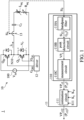
- FIG. 1 shows an exemplary embodiment of an electronic device.
- an electronic device 1 comprises a resonant circuit 10, a power detection circuit 11, a driver 12, and a current sensor 13.
- the power detection circuit 11 is used to detect current total input power of the resonant circuit 10.
- the electronic device 1 may be any device that needs to convert energy using a resonant circuit, such as a wireless signal transceiver, an induction cooker, and the like.
- the technical features of the present application will be described by taking the electronic device 1 as an induction cooker as an example.
- the resonant circuit 10 is coupled to a voltage source 100 to receive an input voltage V in .
- the resonant circuit 10 comprises an upper-arm switching element Q H , a lower-arm switching element Q L , a resonant capacitor Cr, an inductor L eq , and a resistor R eq .
- the upper-arm switching element Q H and the lower-arm switching element Q L are connected in series between the positive terminal and the negative terminal of the voltage source 100.
- the driver 12 generates switching signals G OH and G OL to control the on/off states of the upper-arm switching element Q H and the lower-arm switching element Q L , respectively.
- each of the switching signals G OH and G OL has a duty cycle, so that the controlled upper-arm switching element Q H and the lower-arm switching element Q L operate according to their corresponding duty cycles.
- each of the upper-arm switching element Q H and the lower-arm switching element Q L is switched between the on state and the off state, and the on time of the upper-arm switching element Q H and the on time of the lower-arm switching element Q L do not overlap.
- the inductor L eq and the resistor R eq in the resonant circuit 10 are the equivalent inductance and equivalent resistance of the pot placed on the electronic device (the induction cooker) 1, respectively.
- the resonant capacitor Cr, inductor L eq , and resistor R eq which are connected in series, form a resonant slot of the resonant circuit 10.
- the resonant circuit 10 is coupled to the common node N10 between the upper-arm switching element Q H and the lower-arm switching element Q L .
- a resonant-slot voltage v r is generated between the drain and the source of the lower-arm switching element Q L , and a resonant-slot current i r flows through the capacitor C r .
- the resonant-slot current i r flows from the common node N10 to the resonant slot. It can be discerned from the circuit structure of the resonant circuit 10 that the resonant circuit 10 is a half-bridge series resonant circuit.
- the current sensor 13 is coupled to the resonant slot of the resonant circuit 10 at the common node N10 to sense the resonant-slot current ir.
- the current sensor 13 generates a current signal Si r according to the sensed resonant-slot current ir.
- the current sensor 13 is arranged outside the power detection circuit 11. In other embodiments, the current sensor 13 may be included within the power detection circuit 11.
- the power detection circuit 11 comprises a detection circuit 110 and an estimation circuit 111.
- the detection circuit 110 receives the current signal Si r and obtains baseband power P r1 of the resonant slot according to the current signal Si r to generate the baseband power value VP r1 .
- the estimation circuit 111 receives the baseband power value VP r1 and estimates current total input power P r12 of the resonant slot according to the baseband power value VP r1 to generate an estimated power value VP r12 .
- the detailed operations of the detection circuit 110 and the estimation circuit 111 will be described below.
- the detection circuit 110 comprises a bandpass filter 110A, a peak detection circuit 110B, and a measurement circuit 110C.
- the bandpass filter 110A receives the current signal Si r from the current sensor 13 and performs a bandpass filtering operation on the current signal Si r to obtain a baseband current i r1 of the resonant slot (that is, the baseband component of the resonant-slot current i r ).
- the bandpass filter 110A generates a baseband current signal Si r1 representing the baseband current i r1 , and outputs it to the peak detection circuit 110B.
- the peak detection circuit 110B is coupled to the bandpass filter 110A and receives the baseband current signal Si r1 from the bandpass filter 110A. Since the baseband current signal Si r1 represents the baseband current i r1 , the peak detection circuit 110B can detect a peak value VP i of the baseband current i r1 according to the baseband current signal Si r1 . The peak detection circuit 110B transmits the detected peak value VP i to the measurement circuit 110C.
- the measurement circuit 110C is coupled to the peak detection circuit 110B and receives the peak value VP i .
- the parameter i r1 baseband current
- the measurement circuit 110C After the baseband power P r1 is calculated, the measurement circuit 110C generates the corresponding baseband power value VP r1 and transmits it to the estimation circuit 111.
- the value of the baseband resistance R 1 is predetermined and stored in the measurement circuit 110C in advance. In other embodiments, the value of the baseband resistance R 1 is predetermined and may be stored in a memory (not shown) of the electronic device 1 in advance. When the power detection circuit 11 operates, the value of the baseband resistance R 1 is read from the memory.
- the estimation circuit 111 is coupled to the measurement circuit 110C and receives the baseband power value VP r1 .
- the estimation circuit 111 obtains the baseband power P r1 of the resonant slot according to the baseband power value VP r1 .
- the estimation circuit 111 also receives an indication signal S11 which represents the duty cycle of the switching signal G OH .
- the estimation circuit 111 determines whether the duty cycle of the switching signal G OH is greater than a threshold value (for example, 30% or 50%) according to the indication signal S11.
- the estimation circuit 111 compensates the baseband power P r1 by a compensation parameter K to obtain the estimated current total input power P r12 , and it generates an estimated power value VP r12 according to the estimated current total input power P r12 . In cases where it is determined that the duty cycle of the switching signal G OH is greater than the threshold value, the estimation circuit 111 directly uses the baseband power value VP r1 as the estimated power value VP r12 .
- the compensation parameter K is equal to the ratio of the predetermined frequency-doubling power to the predetermined baseband power of the resonant slot at a specific duty cycle D.
- the compensation parameter K is predetermined and can be stored in the estimation circuit 111 in advance.
- the value of the compensation parameter is a predetermined parameter, which may be stored in a memory (not shown) of the electronic device 1 in advance. When the power detection circuit 11 operates, the compensation parameter K is read from the memory.
- the current total input power P r12 (the estimated power value VP r12 ) obtained in the present application is obtained with high accuracy.
- FIG. 2 shows the resonant-slot voltage v r of the resonant circuit 10 and the harmonic components of the resonant-slot voltage v r .
- the maximum value of the resonant-slot voltage v r is the input voltage V in .
- v r1 represents the baseband component of the resonant-slot voltage v r (also called the baseband voltage of the resonant slot)
- v r2 represents the frequency-doubling component of the resonant-slot voltage v r (also called the frequency-doubling voltage of the resonant slot)
- v r3 represents the frequency-tripling component of the resonant-slot voltage v r (also called the frequency-tripling component of the resonant slot).
- the peak values of the baseband voltage v r1 , the frequency-doubling voltage v r2 , and the frequency-tripling voltage v r3 are 0.5 ⁇ 5 V in , 0.303 V in , and 0.066 V in , respectively. From these values, it can be observed that the peak value of the baseband voltage v r1 is greater than the peak value of the frequency-doubling voltage v r2 and is much larger than the peak value of the frequency-tripling voltage v r3 . Therefore, the influence of the frequency-tripling voltage v r3 can be ignored for the power detection.
- the input impedance of the resonant slot increases with the increase of the operation frequency of the resonant circuit 10 it is only necessary to consider the effect of the low-order voltage harmonics (that is, the baseband harmonic and frequency-doubling harmonic) on the total input power of the resonant slot in response to the above analysis for the baseband voltage v r1 , the frequency-doubling voltage v r2 , and the frequency-tripling voltage v r3 .
- FIG. 4 shows the percentages of the baseband power P r1 , the frequency-doubling power P r2 , the frequency-tripling power P r3 , the coil loss power P coil , and the stray loss power P stray in the total power P r when the duty cycle D is 10%, 20%, 30%, 40%, and 50%, respectively.
- the duty cycle D is 10%, 20%, 30%, 40%, and 50%, respectively.
- the baseband power P r1 accounts for less than 90% of the total power P r
- the frequency-tripling power P r3 , the coil loss power P coil , and the stray loss power P stray each accounts for less than 5% of the total power P r .
- the duty cycle D is greater than 30%
- the baseband power P r1 is almost equal to the total power P r
- the frequency-doubling power P r2 , the frequency-tripling power P r3 , the coil loss power P coil , and the stray loss power P stray each also accounts for less than 5% of the total power P r .
- the estimation circuit 111 does not need to compensate the baseband power P r1 and directly uses the baseband power value VP r1 as the estimated power value VP r12 , so that the current total input power P r12 of the resonant circuit 10 can be accurately estimated.
- the baseband power P r1 accounts for less than 90% of the total power P r and the frequency-doubling power P r2 still accounts for a considerable proportion in the total power P r .
- the estimation circuit 111 compensates the baseband power P r1 using the compensation parameter K to obtain the estimated power value VP r12 .
- the estimation circuit 111 sets a threshold value and determines whether to compensate the baseband power P r1 according to whether the duty cycle D is greater than the threshold value.
- the threshold can be set to 30%.
- the compensation parameter K is the ratio of the frequency-doubling power P r2 to the baseband power P r1 .
- the parameter K v is related to the ratio of the frequency-doubling voltage v r2 to the baseband voltage v r1
- the parameter K 1 is related to the ratio of the frequency-doubling resistance and the baseband resistance.
- Equation (8) it can be known that when the duty cycle D is larger, the proportion of the double frequency power Pr2 is lower, which means that the error which is induced when the current total input power P r12 is estimated according to the baseband power P r1 is smaller.
- the parameter K 1 is determined according to the parameters K L and K R .
- FIG. 5 shows errors of parameters K L and K R and corresponding parameter K 1 under a general operation of an induction cooker. As shown in Fig. 5 , within a wide variation range of the parameters K L and K R (the areas marked with dots in FIG. 5 ), the error of parameter K 1 is less than 10%, which means that the variation range of the parameter K 1 is not large.
- the parameter K 1 can be regarded as a parameter not affected by the duty cycle D.
- the electronic device 1 can first obtain the compensation parameter K at a specific duty cycle D through a test or analysis, then obtain the parameter K v according to Equation (8), and finally estimate the parameter K 1 is according to the compensation parameter K and the parameter K v .
- the obtained compensation parameter K and the parameters K v and K 1 are stored in a memory of the electronic device 1 or stored in the estimation circuit 111 as predetermined parameters which can be used by the power detection circuit 11 during the operation.
- the electronic device 1 predetermines the compensation parameter K and the parameters K v and K 1 which all correspond to the duty cycle D of 10%.
- the estimation circuit 111 sets the threshold value as 30% as a criterion for determining whether to compensate the baseband power P r1 .
- the electronic device 1 may predetermine a plurality of compensation parameters K and a plurality of parameters K v and K 1 corresponding to a plurality of duty cycles as the predetermined parameters.
- one compensation parameter K or one set of parameters K v and K 1 among the predetermined parameters can be selected according to the indication signal S11 which represents the duty cycle D of the switching signal G OH to compensate the baseband power P r1 .
- the estimation circuit 11 determines whether to compensate the baseband power P r1 according to whether the duty cycle D is greater than a threshold value. In other embodiments, regardless of the duty cycle D of the switching signal G OH , the estimation circuit 111 compensates the baseband power P r1 according to the compensation parameter K to obtain the estimated current total input power P r12 , and generates the estimated power value VP r12 according to the estimated current total input power P r12 .
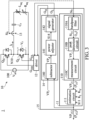
- FIG. 3 shows another exemplary embodiment of an electronic device.
- the electronic device 3 comprises a resonant circuit 10, a power detection circuit 11, a driver 12 , and a current sensor 13 as shown in FIG. 1 .
- the operations of the resonant circuit 10, the power detection circuit 11, the driver 12, and the current sensor 13 are described in the paragraphs related to the embodiment of FIG. 1 , and the description is omitted here.
- the electronic device 3 further comprises an adjustment circuit 14.
- a control circuit 15 is composed of the power detection circuit 11 and the adjustment circuit 14 for controlling the resonant circuit 10.
- the adjustment circuit 14 receives the estimated power value VP r12 from the estimation circuit 111 and generates the control signals G H and G L .
- the adjustment circuit 14 calculates a power difference between the estimated power value VP r12 and the preset power value VP r and adjusts the respective duty cycles of the control signals G H and G L according to the power difference.
- the current sensor 13 is arranged outside the control circuit 15. In other embodiments, the current sensor 13 may be included within the control circuit 15.
- the driver 12 receives the control signals G H and G L from the adjustment circuit 14 and generates the switching signals G OH and G OL according to the control signals G H and G L to control the on/off states of the upper-arm switching element Q H and the lower-arm switching element Q L , respectively. Therefore, the adjustment circuit 14 adjusts or changes the respective duty cycles of the switching signals G OH and G OL by adjusting the respective duty cycles of the control signals G H and G L .
- the duty cycle of the control signal G H is equal to the duty cycle (D) of the switching signal G OH
- the duty cycle of the control signal G L is equal to the duty cycle of the switching signal G OL .
- the adjustment circuit 14 includes a subtractor 140, a power adjuster 141, and a signal generator 142.
- the subtractor 140 receives the estimated power value VP r12 and the preset power value VP r and calculates the difference between the estimated power value VP r12 and the preset power value VP r to generate a power difference value VP d .
- the subtractor 140 transmits the power difference value VP d to the power adjuster 141.
- the power adjuster 141 receives the power difference VP d and generates an adjustment signal S14 according to at least one feature of the power difference VP d .
- the at least one feature of the power difference VP d comprises at least one of the magnitude of the power difference VP d and the polarity (positive or negative) thereof.
- the adjustment signal S14 indicates how to adjust the duty cycles of the control signals G H and G L .
- the adjustment signal S14 indicates at least one of an adjustment range and an adjustment direction (whether increasing or decreasing) for adjusting the duty cycles of the control signals G H and G L .
- the power adjuster 141 provides the adjustment signal S14 to the signal generator 142.
- the signal generator 142 receives the adjustment signal S14 and generates the control signals G H and G L .
- the signal generator 142 adjusts the duty cycles of the control signals G H and G L according to the adjustment signal S14.
- the signal generator 142 provides the control signals G H and G L to the driver 12.
- the driver 12 generates switching signals G OH and G OL according to the control signals G H and G L to control the on/off states of the upper-arm switching element Q H and the lower-arm switching element Q L , respectively.
- the control circuit 15 can estimate the current total input power P r12 of the resonant circuit 10 according to the baseband power value VP r1 to generate the estimated power value VP r12 .
- the duty cycles of the control signals G H and G L are adjusted based on the difference between the estimated power value VP r12 and the desired preset power value VP r , thereby adjusting the switching signals G OH and G OL .
- the current total input power P r12 of the resonant circuit 10 is finally close to or equal to the desired preset power value VPr.
Landscapes
- Engineering & Computer Science (AREA)
- Physics & Mathematics (AREA)
- General Physics & Mathematics (AREA)
- Power Engineering (AREA)
- Electromagnetism (AREA)
- Radar, Positioning & Navigation (AREA)
- Automation & Control Theory (AREA)
- General Engineering & Computer Science (AREA)
- Inverter Devices (AREA)
- Transmitters (AREA)
Abstract
Description
- This Application claims priority of
China Patent Application No. 202111652210.5, filed on December 30, 2021 - The present invention relates to a power detection circuit, and more particularly to a control circuit for controlling a resonant circuit in response to detection of a resonant-slot baseband power.
- Resonant circuits are circuits used in electronic systems to convert energy. For example, resonant circuits are often used in transmission and reception devices for wireless signals, power converters, and the like. When a device uses a resonant circuit, the input power of the resonant slot in the resonant circuit determines the performance of the device. Therefore, it is necessary to detect the input power of the resonant slot, and control or adjust the subsequent circuits or devices of the device according to the detection result. However, in existing methods of detecting the input power of a resonant slot, the current and voltage of the resonant slot are usually obtained using high-speed sampling, multiplication, integration, and averaging, which increases the complexity of the operation and requires a high-level operation processor.
- Thus, the present invention provides a power detection circuit and a control circuit, which estimate input power of a resonant slot of a resonant circuit using resonant-slot baseband power and control the resonant circuit accordingly.
- An exemplary embodiment of the present invention provides a power detection circuit for detecting current total input power of a resonant circuit. The power detection circuit comprises a detection circuit and an estimation circuit. The detection circuit receives a current signal and obtains resonant-slot baseband power according to the current signal to generate the baseband power value. The current signal represents a resonant-slot current generated by the resonant circuit. The estimation circuit receives the baseband power value and estimates the current total input power according to the baseband power value to generate an estimated power value.
- Another exemplary embodiment of the present invention provides a control circuit for generating a first control signal to control a resonant circuit. The control circuit comprises a detection circuit, an estimation circuit, and an adjustment circuit. The detection circuit receives the current signal and obtains resonant-slot baseband power according to the current signal to generate a baseband power value. The current signal represents a resonant-slot current generated by the resonant circuit. The estimation circuit receives the baseband power value and estimates a current total input power of the resonant circuit according to the baseband power value to generate an estimated power value. The adjustment circuit receives the estimated power value and generates the first control signal. The adjustment circuit calculates a power difference between the estimated power value and a preset power value and adjusts a duty cycle of the first control signal according to the power difference.
- A detailed description is given in the following embodiments with reference to the accompanying drawings.
- The invention can be more fully understood by reading the subsequent detailed description and examples with references made to the accompanying drawings, wherein:
-
FIG. 1 shows one exemplary embodiment of an electronic device comprising a resonant circuit and a power detection circuit; -
FIG. 2 shows a resonant-slot voltage of the resonant circuit inFIG. 1 and harmonic components of the resonant-slot voltage; -
FIG. 3 shows another exemplary embodiment of an electronic device comprising a resonant circuit, a power detection circuit, and an adjustment circuit; -
FIG. 4 shows percentages of baseband power, frequency-doubling power, frequency-tripling power, coil loss power, and stray loss power of the resonant slot in relative to total power at different duty cycles of the resonant circuit; and -
FIG. 5 shows errors of parameters KL and KR and corresponding parameter K1 under a general operation of an induction cooker. - The following description is of the best-contemplated model of carrying out the invention. This description is made for the purpose of illustrating the general principles of the invention and should not be taken in a limiting sense. The scope of the invention is best determined by reference to the appended claims.
-
FIG. 1 shows an exemplary embodiment of an electronic device. Referring toFIG. 1 , anelectronic device 1 comprises aresonant circuit 10, apower detection circuit 11, adriver 12, and acurrent sensor 13. Thepower detection circuit 11 is used to detect current total input power of theresonant circuit 10. In an embodiment, theelectronic device 1 may be any device that needs to convert energy using a resonant circuit, such as a wireless signal transceiver, an induction cooker, and the like. Hereinafter, the technical features of the present application will be described by taking theelectronic device 1 as an induction cooker as an example. - Referring to
FIG. 1 , theresonant circuit 10 is coupled to avoltage source 100 to receive an input voltage Vin. Theresonant circuit 10 comprises an upper-arm switching element QH, a lower-arm switching element QL, a resonant capacitor Cr, an inductor Leq, and a resistor Req. The upper-arm switching element QH and the lower-arm switching element QL are connected in series between the positive terminal and the negative terminal of thevoltage source 100. Thedriver 12 generates switching signals GOH and GOL to control the on/off states of the upper-arm switching element QH and the lower-arm switching element QL, respectively. In the embodiment, each of the switching signals GOH and GOL has a duty cycle, so that the controlled upper-arm switching element QH and the lower-arm switching element QL operate according to their corresponding duty cycles. Through the control of the switching signals GOH and GOL, each of the upper-arm switching element QH and the lower-arm switching element QL is switched between the on state and the off state, and the on time of the upper-arm switching element QH and the on time of the lower-arm switching element QL do not overlap. - Referring to
FIG. 1 , in cases where theelectronic device 1 is an induction cooker, the inductor Leq and the resistor Req in theresonant circuit 10 are the equivalent inductance and equivalent resistance of the pot placed on the electronic device (the induction cooker) 1, respectively. The resonant capacitor Cr, inductor Leq, and resistor Req, which are connected in series, form a resonant slot of theresonant circuit 10. Theresonant circuit 10 is coupled to the common node N10 between the upper-arm switching element QH and the lower-arm switching element QL. By controlling each of the upper-arm switching element QH and the lower-arm switching element QL to switch between the on state and the off state, a resonant-slot voltage vr is generated between the drain and the source of the lower-arm switching element QL, and a resonant-slot current ir flows through the capacitor Cr. As shown inFIG. 1 , the resonant-slot current ir flows from the common node N10 to the resonant slot. It can be discerned from the circuit structure of theresonant circuit 10 that theresonant circuit 10 is a half-bridge series resonant circuit. - As shown in
FIG. 1 , thecurrent sensor 13 is coupled to the resonant slot of theresonant circuit 10 at the common node N10 to sense the resonant-slot current ir. Thecurrent sensor 13 generates a current signal Sir according to the sensed resonant-slot current ir. In the embodiment ofFIG. 1 , thecurrent sensor 13 is arranged outside thepower detection circuit 11. In other embodiments, thecurrent sensor 13 may be included within thepower detection circuit 11. - The
power detection circuit 11 comprises adetection circuit 110 and anestimation circuit 111. Thedetection circuit 110 receives the current signal Sir and obtains baseband power Pr1 of the resonant slot according to the current signal Sir to generate the baseband power value VPr1. Theestimation circuit 111 receives the baseband power value VPr1 and estimates current total input power Pr12 of the resonant slot according to the baseband power value VPr1 to generate an estimated power value VPr12. The detailed operations of thedetection circuit 110 and theestimation circuit 111 will be described below. - Referring to
FIG. 1 , thedetection circuit 110 comprises abandpass filter 110A, apeak detection circuit 110B, and ameasurement circuit 110C. Thebandpass filter 110A receives the current signal Sir from thecurrent sensor 13 and performs a bandpass filtering operation on the current signal Sir to obtain a baseband current ir1 of the resonant slot (that is, the baseband component of the resonant-slot current ir). Thebandpass filter 110A generates a baseband current signal Sir1 representing the baseband current ir1, and outputs it to thepeak detection circuit 110B. - The
peak detection circuit 110B is coupled to thebandpass filter 110A and receives the baseband current signal Sir1 from thebandpass filter 110A. Since the baseband current signal Sir1 represents the baseband current ir1, thepeak detection circuit 110B can detect a peak value VPi of the baseband current ir1 according to the baseband current signal Sir1. Thepeak detection circuit 110B transmits the detected peak value VPi to themeasurement circuit 110C. - The
measurement circuit 110C is coupled to thepeak detection circuit 110B and receives the peak value VPi. Themeasurement circuit 110C measures the baseband power
measurement circuit 110C generates the corresponding baseband power value VPr1 and transmits it to theestimation circuit 111. In the embodiment, the value of the baseband resistance R1 is predetermined and stored in themeasurement circuit 110C in advance. In other embodiments, the value of the baseband resistance R1 is predetermined and may be stored in a memory (not shown) of theelectronic device 1 in advance. When thepower detection circuit 11 operates, the value of the baseband resistance R1 is read from the memory. - The
estimation circuit 111 is coupled to themeasurement circuit 110C and receives the baseband power value VPr1. Theestimation circuit 111 obtains the baseband power Pr1 of the resonant slot according to the baseband power value VPr1. Theestimation circuit 111 also receives an indication signal S11 which represents the duty cycle of the switching signal GOH. In the embodiment, theestimation circuit 111 determines whether the duty cycle of the switching signal GOH is greater than a threshold value (for example, 30% or 50%) according to the indication signal S11. In the case where it is determined that the duty cycle of the switching signal GOH is not greater than the threshold value, theestimation circuit 111 compensates the baseband power Pr1 by a compensation parameter K to obtain the estimated current total input power Pr12, and it generates an estimated power value VPr12 according to the estimated current total input power Pr12. In cases where it is determined that the duty cycle of the switching signal GOH is greater than the threshold value, theestimation circuit 111 directly uses the baseband power value VPr1 as the estimated power value VPr12. - In the embodiment, the compensation parameter K is equal to the ratio of the predetermined frequency-doubling power to the predetermined baseband power of the resonant slot at a specific duty cycle D. The compensation parameter K is predetermined and can be stored in the
estimation circuit 111 in advance. In other embodiments, the value of the compensation parameter is a predetermined parameter, which may be stored in a memory (not shown) of theelectronic device 1 in advance. When thepower detection circuit 11 operates, the compensation parameter K is read from the memory. - According to the embodiments of the present application, only the baseband power of the resonant slot is required for estimating the current total input power Pr12 of the resonant slot without complex calculations. Moreover, due to the compensation mechanism of the
estimation circuit 111, the current total input power Pr12 (the estimated power value VPr12) obtained in the present application is obtained with high accuracy. - The following will describe the analysis related to how the
power detection circuit 11 of the present application can obtain the accurate current total input power Pr12 according to the baseband power of the resonant slot. -
FIG. 2 shows the resonant-slot voltage vr of theresonant circuit 10 and the harmonic components of the resonant-slot voltage vr. Referring toFIG. 2 , the maximum value of the resonant-slot voltage vr is the input voltage Vin. vr1 represents the baseband component of the resonant-slot voltage vr (also called the baseband voltage of the resonant slot), vr2 represents the frequency-doubling component of the resonant-slot voltage vr (also called the frequency-doubling voltage of the resonant slot), and vr3 represents the frequency-tripling component of the resonant-slot voltage vr (also called the frequency-tripling component of the resonant slot). The resonant-slot voltage vr can be expressed as:
- fs represents the switching frequency of the resonant-slot voltage vr;
-

- D represents the duty cycle of the switching signal GOH (that is, the ratio of the turned-on time of the upper-arm switching element QH to the period).
- Equation (1) is expressed based on Fourier series as:


- Vin represents the maximum value of the square wave of the resonant-slot voltage vr (that is, the input voltage);
- n represents the harmonic order of the resonant-slot voltage vr; and
- θn represents n-th harmonic phase angle.
- Assuming that the duty cycle D is equal to 30% as an example. After D=0.3 is applied to Equation (2), we get:

- In cases where only the peak values (maximum values) of the voltage is considered, the peak values of the baseband voltage vr1, the frequency-doubling voltage vr2, and the frequency-tripling voltage vr3 are 0.5\5Vin , 0.303Vin , and 0.066Vin , respectively. From these values, it can be observed that the peak value of the baseband voltage vr1 is greater than the peak value of the frequency-doubling voltage vr2 and is much larger than the peak value of the frequency-tripling voltage vr3. Therefore, the influence of the frequency-tripling voltage vr3 can be ignored for the power detection.
- Since the input impedance of the resonant slot increases with the increase of the operation frequency of the
resonant circuit 10 it is only necessary to consider the effect of the low-order voltage harmonics (that is, the baseband harmonic and frequency-doubling harmonic) on the total input power of the resonant slot in response to the above analysis for the baseband voltage vr1, the frequency-doubling voltage vr2, and the frequency-tripling voltage vr3. - The applicant of the present application simulated the power distribution of the
resonant circuit 10.FIG. 4 shows the percentages of the baseband power Pr1, the frequency-doubling power Pr2, the frequency-tripling power Pr3, the coil loss power Pcoil, and the stray loss power Pstray in the total power Pr when the duty cycle D is 10%, 20%, 30%, 40%, and 50%, respectively. As shown inFIG. 4 , when the duty cycle D is equal to or less than 30%, the baseband power Pr1 accounts for less than 90% of the total power Pr, and the frequency-tripling power Pr3, the coil loss power Pcoil, and the stray loss power Pstray each accounts for less than 5% of the total power Pr. When the duty cycle D is greater than 30%, the baseband power Pr1 is almost equal to the total power Pr, and the frequency-doubling power Pr2, the frequency-tripling power Pr3, the coil loss power Pcoil, and the stray loss power Pstray each also accounts for less than 5% of the total power Pr. - According to the above analysis, when the duty cycle D is large, since the baseband power Pr1 is almost equal to the total power Pr, the
estimation circuit 111 does not need to compensate the baseband power Pr1 and directly uses the baseband power value VPr1 as the estimated power value VPr12, so that the current total input power Pr12 of theresonant circuit 10 can be accurately estimated. As mentioned above, when the duty cycle D is small, the baseband power Pr1 accounts for less than 90% of the total power Pr and the frequency-doubling power Pr2 still accounts for a considerable proportion in the total power Pr. In order to more accurately estimate the current total input power Pr12 according to the baseband power Pr1, theestimation circuit 111 compensates the baseband power Pr1 using the compensation parameter K to obtain the estimated power value VPr12. - In an embodiment, the
estimation circuit 111 sets a threshold value and determines whether to compensate the baseband power Pr1 according to whether the duty cycle D is greater than the threshold value. According to the above description, the threshold can be set to 30%. - The definition of the compensation parameter K will be described below.
- Assuming that the current total input power Pr12 is estimated by the baseband power Pr1 and the frequency-doubling power Pr2 of the resonant slot, Pr12 can be expressed as:


-
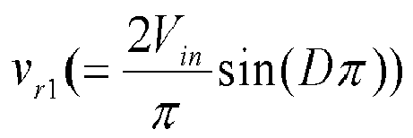
-

-

-

- R 1 , R 2 represent the baseband resistance and the frequency- doubling resistance of the resonant slot respectively;
- L 1 , L 2 represent the baseband inductance and the frequency-doubling inductance of the resonant slot respectively;
- ωs represents the operation angular velocity.
- According to Equation (4) and Equation (7), the compensation parameter K is the ratio of the frequency-doubling power Pr2 to the baseband power Pr1. According to Equation (5), Equation (7), and Equation (8), the parameter Kv is related to the ratio of the frequency-doubling voltage vr2 to the baseband voltage vr1, and the parameter K1 is related to the ratio of the frequency-doubling resistance and the baseband resistance. When the duty cycle D is 10%, 20%, and 30%, the parameter Kv is 0.9, 0.65, and 0.35, respectively. Therefore, according to Equation (8), it can be known that when the duty cycle D is larger, the proportion of the double frequency power Pr2 is lower, which means that the error which is induced when the current total input power Pr12 is estimated according to the baseband power Pr1 is smaller.
- According to the above, when the duty cycle D is smaller, the parameter Kv is larger, that is, the proportion of the frequency-doubling power Pr2 is larger. Therefore, when the current total input power Pr12 is estimated according to the baseband power Pr1, the baseband power Pr1 needs to be compensated. In the embodiment of the present application, the compensation parameter K is used to compensate the baseband power Pr1, wherein the compensation parameter K is equal to the ratio of the frequency-doubling power Pr2 to the baseband power Pr1 and further equal to the product of the parameters Kv and K1 (K= Kv K1).
- According to Equation (10) to Equation (12), the parameter K1 is determined according to the parameters KL and KR.
FIG. 5 shows errors of parameters KL and KR and corresponding parameter K1 under a general operation of an induction cooker. As shown inFig. 5 , within a wide variation range of the parameters KL and KR (the areas marked with dots inFIG. 5 ), the error of parameter K1 is less than 10%, which means that the variation range of the parameter K1 is not large. The parameter K1 can be regarded as a parameter not affected by the duty cycle D. Therefore, according to the embodiment of the present application, theelectronic device 1 can first obtain the compensation parameter K at a specific duty cycle D through a test or analysis, then obtain the parameter Kv according to Equation (8), and finally estimate the parameter K1 is according to the compensation parameter K and the parameter Kv. The obtained compensation parameter K and the parameters Kv and K1 are stored in a memory of theelectronic device 1 or stored in theestimation circuit 111 as predetermined parameters which can be used by thepower detection circuit 11 during the operation. - In an embodiment, the
electronic device 1 predetermines the compensation parameter K and the parameters Kv and K1 which all correspond to the duty cycle D of 10%. In this case, theestimation circuit 111 sets the threshold value as 30% as a criterion for determining whether to compensate the baseband power Pr1. - In other embodiments, the
electronic device 1 may predetermine a plurality of compensation parameters K and a plurality of parameters Kv and K1 corresponding to a plurality of duty cycles as the predetermined parameters. When thepower detection circuit 11 operates, one compensation parameter K or one set of parameters Kv and K1 among the predetermined parameters can be selected according to the indication signal S11 which represents the duty cycle D of the switching signal GOH to compensate the baseband power Pr1. - In the above embodiment, the
estimation circuit 11 determines whether to compensate the baseband power Pr1 according to whether the duty cycle D is greater than a threshold value. In other embodiments, regardless of the duty cycle D of the switching signal GOH, theestimation circuit 111 compensates the baseband power Pr1 according to the compensation parameter K to obtain the estimated current total input power Pr12, and generates the estimated power value VPr12 according to the estimated current total input power Pr12. -
FIG. 3 shows another exemplary embodiment of an electronic device. Referring toFIG. 3 , theelectronic device 3 comprises aresonant circuit 10, apower detection circuit 11, adriver 12 , and acurrent sensor 13 as shown inFIG. 1 . The operations of theresonant circuit 10, thepower detection circuit 11, thedriver 12, and thecurrent sensor 13 are described in the paragraphs related to the embodiment ofFIG. 1 , and the description is omitted here. - As shown in
FIG. 3 , theelectronic device 3 further comprises anadjustment circuit 14. Acontrol circuit 15 is composed of thepower detection circuit 11 and theadjustment circuit 14 for controlling theresonant circuit 10. Theadjustment circuit 14 receives the estimated power value VPr12 from theestimation circuit 111 and generates the control signals GH and GL. Theadjustment circuit 14 calculates a power difference between the estimated power value VPr12 and the preset power value VPr and adjusts the respective duty cycles of the control signals GH and GL according to the power difference. - In the embodiment of
FIG. 3 , thecurrent sensor 13 is arranged outside thecontrol circuit 15. In other embodiments, thecurrent sensor 13 may be included within thecontrol circuit 15. - The
driver 12 receives the control signals GH and GL from theadjustment circuit 14 and generates the switching signals GOH and GOL according to the control signals GH and GL to control the on/off states of the upper-arm switching element QH and the lower-arm switching element QL, respectively. Therefore, theadjustment circuit 14 adjusts or changes the respective duty cycles of the switching signals GOH and GOL by adjusting the respective duty cycles of the control signals GH and GL. In the embodiment, the duty cycle of the control signal GH is equal to the duty cycle (D) of the switching signal GOH, and the duty cycle of the control signal GL is equal to the duty cycle of the switching signal GOL. - Referring to
FIG. 3 , theadjustment circuit 14 includes asubtractor 140, apower adjuster 141, and asignal generator 142. Thesubtractor 140 receives the estimated power value VPr12 and the preset power value VPr and calculates the difference between the estimated power value VPr12 and the preset power value VPr to generate a power difference value VPd. Thesubtractor 140 transmits the power difference value VPd to thepower adjuster 141. - The
power adjuster 141 receives the power difference VPd and generates an adjustment signal S14 according to at least one feature of the power difference VPd. In the embodiment, the at least one feature of the power difference VPd comprises at least one of the magnitude of the power difference VPd and the polarity (positive or negative) thereof. The adjustment signal S14 indicates how to adjust the duty cycles of the control signals GH and GL. For example, the adjustment signal S14 indicates at least one of an adjustment range and an adjustment direction (whether increasing or decreasing) for adjusting the duty cycles of the control signals GH and GL. Thepower adjuster 141 provides the adjustment signal S14 to thesignal generator 142. - The
signal generator 142 receives the adjustment signal S14 and generates the control signals GH and GL. Thesignal generator 142 adjusts the duty cycles of the control signals GH and GL according to the adjustment signal S14. Thesignal generator 142 provides the control signals GH and GL to thedriver 12. Thedriver 12 generates switching signals GOH and GOL according to the control signals GH and GL to control the on/off states of the upper-arm switching element QH and the lower-arm switching element QL, respectively. - Through the operations of the
power detection circuit 11 and theadjustment circuit 14 in thecontrol circuit 15, thecontrol circuit 15 can estimate the current total input power Pr12 of theresonant circuit 10 according to the baseband power value VPr1 to generate the estimated power value VPr12. The duty cycles of the control signals GH and GL are adjusted based on the difference between the estimated power value VPr12 and the desired preset power value VPr, thereby adjusting the switching signals GOH and GOL. Through the estimation and adjustment operations of thecontrol circuit 15, the current total input power Pr12 of theresonant circuit 10 is finally close to or equal to the desired preset power value VPr. - While the invention has been described by way of example and in terms of the preferred embodiments, it is to be understood that the invention is not limited to the disclosed embodiments. On the contrary, it is intended to cover various modifications and similar arrangements (as would be apparent to those skilled in the art). Therefore, the scope of the appended claims should be accorded the broadest interpretation so as to encompass all such modifications and similar arrangements.


Claims (7)
- A power detection circuit for detecting current total input power of a resonant circuit, comprising:a detection circuit receiving a current signal and obtaining resonant-slot baseband power according to the current signal to generate a baseband power value, wherein the current signal represents a resonant-slot current generated by the resonant circuit; andan estimation circuit receiving the baseband power value and estimating the current total input power according to the baseband power value to generate an estimated power value.
- The power detection circuit as claimed in claim 1, wherein:the resonant circuit comprises a switching element, and the switching element operates according to a duty cycle, andthe estimation circuit obtains the resonant-slot baseband power according to the baseband power value and compensates the resonant-slot baseband power according to a compensation parameter to generate the estimated power value.
- The power detection circuit as claimed in claim 1 or 2, wherein:the resonant circuit comprises a switching element, and the switching element operates according to a duty cycle,when the duty cycle is greater than a threshold value, the estimation circuit receives the baseband power value as the estimated power value,when the duty cycle is not greater than the threshold value, the estimation circuit obtains the resonant-slot baseband power according to the baseband power value and compensates the resonant-slot baseband power according to a compensation parameter to generate the estimated power value, andthe compensation parameter is related to a ratio of a predetermined frequency-doubling power to a predetermined baseband power of the resonant circuit at a specific value of the duty cycle.
- The power detection circuit as claimed in any of the preceding claims, wherein the detection circuit comprises:a bandpass filter receiving the current signal and performing a bandpass filtering operation on the current signal to generate a baseband current signal, wherein the baseband current signal represents a resonant-slot baseband current of the resonant circuit;a peak value detection circuit receiving the baseband current signal and detecting a peak value of the resonant-slot baseband current according to the baseband current signal; anda measuring circuit receiving the peak value and measuring the resonant-slot baseband power according to the peak value and a baseband resistance to generate the baseband power value,wherein the baseband resistance represents a resonant-slot baseband resistance of the resonant circuit.
- A control circuit for generating a first control signal and a second control signal to control a resonant circuit, comprising:a power detection circuit as claimed in any of the preceding claims; andan adjustment circuit receiving the estimated power value and generating the first control signal, wherein the adjustment circuit calculates a power difference between the estimated power value and a preset power value and adjusts a duty cycle of the first control signal according to the power difference,wherein the adjustment circuit further adjusts the second control signal according to the power difference, andwherein the resonant circuit comprises an upper-arm switching element and a lower-arm switching element which are connected in series, the first control signal is applied to control the upper-arm switching element, and the second control signal is applied to control the lower-arm side switching element.
- The control circuit as claimed in claim 5, wherein:when the duty cycle of the first control signal is greater than a threshold value, the estimation circuit receives the baseband power value as the estimated power value,when the duty cycle of the first control signal is not greater than the threshold value, the estimation circuit obtains the resonant-slot baseband power according to the baseband power value and compensates the resonant-slot baseband power according to a compensation parameter to generate the estimated power value, andwherein the compensation parameter is related to a ratio of a predetermined frequency-doubling power to a predetermined baseband power of the resonant circuit at a specific value of the duty cycle.
- The control circuit as claimed in claim 5 or 6, wherein the adjustment circuit comprises:a subtractor receiving the estimated power value and the preset power value and calculating the difference between the estimated power value and the preset power value to generate the power difference value;a power adjuster receiving the power difference and generating an adjustment signal according to at least one feature of the power difference; anda signal generator generating the first control signal, wherein the signal generator receives the adjustment signal and adjusts the duty cycle of the first control signal according to the adjustment signal,wherein the at least one feature of the power difference comprises at least one of a magnitude and a polarity of the power difference, andthe adjustment signal indicates at least one of an adjustment amplitude and an adjustment direction for adjusting the duty cycle.
Applications Claiming Priority (1)
| Application Number | Priority Date | Filing Date | Title |
|---|---|---|---|
| CN202111652210.5A CN116430111B (en) | 2021-12-30 | 2021-12-30 | Power detection circuit and control circuit |
Publications (3)
| Publication Number | Publication Date |
|---|---|
| EP4206702A1 true EP4206702A1 (en) | 2023-07-05 |
| EP4206702B1 EP4206702B1 (en) | 2024-05-08 |
| EP4206702C0 EP4206702C0 (en) | 2024-05-08 |
Family
ID=83271320
Family Applications (1)
| Application Number | Title | Priority Date | Filing Date |
|---|---|---|---|
| EP22194946.4A Active EP4206702B1 (en) | 2021-12-30 | 2022-09-09 | Power detection circuit and control circuit |
Country Status (4)
| Country | Link |
|---|---|
| US (1) | US11789090B2 (en) |
| EP (1) | EP4206702B1 (en) |
| CN (1) | CN116430111B (en) |
| ES (1) | ES2984822T3 (en) |
Cited By (1)
| Publication number | Priority date | Publication date | Assignee | Title |
|---|---|---|---|---|
| EP4733779A1 (en) * | 2024-10-24 | 2026-04-29 | Delta Electronics, Inc. | Electronic device and method to estimate input power into resonant tank in resonant circuit |
Citations (4)
| Publication number | Priority date | Publication date | Assignee | Title |
|---|---|---|---|---|
| US5334941A (en) * | 1992-09-14 | 1994-08-02 | Kdc Technology Corp. | Microwave reflection resonator sensors |
| CN204068705U (en) * | 2014-09-19 | 2014-12-31 | 成都芯源系统有限公司 | Switching power supply circuit |
| US20170315037A9 (en) * | 2013-02-13 | 2017-11-02 | Board Of Regents, The University Of Texas System | Sensor Assembly, Method, and Device for Monitoring Shear Force and Pressure on a Structure |
| US10090884B2 (en) * | 2013-01-11 | 2018-10-02 | Koninklijke Philips N.V. | Wireless inductive power transfer |
Family Cites Families (9)
| Publication number | Priority date | Publication date | Assignee | Title |
|---|---|---|---|---|
| US7906941B2 (en) * | 2007-06-19 | 2011-03-15 | Flextronics International Usa, Inc. | System and method for estimating input power for a power processing circuit |
| US8552808B2 (en) * | 2011-06-02 | 2013-10-08 | Tektronix, Inc. | Apparatus and method for oscillator resonator power control |
| JP5886025B2 (en) | 2011-12-20 | 2016-03-16 | ルネサスエレクトロニクス株式会社 | RF power amplifier and method of operating the same |
| CN102647104A (en) * | 2012-04-13 | 2012-08-22 | 美的集团有限公司 | Power control device and control method of half-bridge resonant circuit |
| CN105790626B (en) * | 2014-12-25 | 2019-02-12 | 台达电子工业股份有限公司 | Resonant type power conversion circuit and method of controlling resonant type power conversion circuit |
| CN110214410A (en) * | 2016-11-22 | 2019-09-06 | 电力集成公司 | Switch control for resonance power converter |
| US10686382B2 (en) * | 2017-01-05 | 2020-06-16 | Stmicroelectronics S.R.L. | Symmetric time shift control for resonant converters |
| TWI694670B (en) * | 2019-02-15 | 2020-05-21 | 群光電能科技股份有限公司 | Resonant power convertor |
| US11280847B1 (en) * | 2020-10-30 | 2022-03-22 | Taiwan Semiconductor Manufacturing Company Ltd. | Circuit, semiconductor device and method for parameter PSRR measurement |
-
2021
- 2021-12-30 CN CN202111652210.5A patent/CN116430111B/en active Active
-
2022
- 2022-04-25 US US17/728,551 patent/US11789090B2/en active Active
- 2022-09-09 ES ES22194946T patent/ES2984822T3/en active Active
- 2022-09-09 EP EP22194946.4A patent/EP4206702B1/en active Active
Patent Citations (4)
| Publication number | Priority date | Publication date | Assignee | Title |
|---|---|---|---|---|
| US5334941A (en) * | 1992-09-14 | 1994-08-02 | Kdc Technology Corp. | Microwave reflection resonator sensors |
| US10090884B2 (en) * | 2013-01-11 | 2018-10-02 | Koninklijke Philips N.V. | Wireless inductive power transfer |
| US20170315037A9 (en) * | 2013-02-13 | 2017-11-02 | Board Of Regents, The University Of Texas System | Sensor Assembly, Method, and Device for Monitoring Shear Force and Pressure on a Structure |
| CN204068705U (en) * | 2014-09-19 | 2014-12-31 | 成都芯源系统有限公司 | Switching power supply circuit |
Non-Patent Citations (1)
| Title |
|---|
| HELEN N SCHWERDT ET AL: "A Fully Passive Wireless Microsystem for Recording of Neuropotentials Using RF Backscattering Methods", JOURNAL OF MICROELECTROMECHANICAL SYSTEMS, IEEE SERVICE CENTER, US, vol. 20, no. 5, 1 October 2011 (2011-10-01), pages 1119 - 1130, XP011360781, ISSN: 1057-7157, DOI: 10.1109/JMEMS.2011.2162487 * |
Cited By (1)
| Publication number | Priority date | Publication date | Assignee | Title |
|---|---|---|---|---|
| EP4733779A1 (en) * | 2024-10-24 | 2026-04-29 | Delta Electronics, Inc. | Electronic device and method to estimate input power into resonant tank in resonant circuit |
Also Published As
| Publication number | Publication date |
|---|---|
| EP4206702B1 (en) | 2024-05-08 |
| US11789090B2 (en) | 2023-10-17 |
| ES2984822T3 (en) | 2024-10-31 |
| US20230213591A1 (en) | 2023-07-06 |
| CN116430111B (en) | 2025-12-05 |
| CN116430111A (en) | 2023-07-14 |
| EP4206702C0 (en) | 2024-05-08 |
Similar Documents
| Publication | Publication Date | Title |
|---|---|---|
| US10132846B2 (en) | Method of and apparatus for learning the phase error or timing delays within a current transducer and power measurement apparatus including current transducer error correction | |
| RU2608329C2 (en) | Method and device for measuring electric current using current converter | |
| US9733061B2 (en) | Distance determination based on reflected admittance | |
| US7511471B2 (en) | Magnetic bridge electric power sensor | |
| US10527666B2 (en) | Method and device for determining the fault location in the case of a fault on an electric line | |
| EP4206702B1 (en) | Power detection circuit and control circuit | |
| US20260058499A1 (en) | Foreign object detection and related apparatuses, methods, and systems | |
| EP4113144B1 (en) | Leakage current detection circuit and method, and leakage current detector | |
| US4055803A (en) | Combined watt and var transducer | |
| EP1777530B1 (en) | Method and arrangement for measuring inverter output currents | |
| JP7185872B2 (en) | Displacement sensor | |
| US10527653B2 (en) | Ultra-high bandwidth current shunt | |
| US6195274B1 (en) | Method for defining instantaneous value of current of pulse-controlled inductive load | |
| US12519347B2 (en) | Foreign object detection by frequency bandwidth comparison | |
| US11486749B2 (en) | Time-of-flight generating circuit and chip, flow meter and method of the same | |
| CN107589297B (en) | Active current detection and frequency tracking circuit of ultrasonic transducer | |
| TWI796918B (en) | Power detection circuit and control circuit | |
| US20250362326A1 (en) | High-bandwidth current sensor with adaptive compensation for parasitic resistance | |
| US10585055B2 (en) | Method for operating an inductive conductivity meter and respective conductivity meter | |
| NL7907407A (en) | INSTRUMENTATION SYSTEM. | |
| US20240396420A1 (en) | Power converter | |
| SU1698739A2 (en) | Eddy-current measuring device | |
| CN121308377A (en) | Mutual inductance and load voltage identification circuit and identification method for wireless power transmission systems | |
| JPH05240715A (en) | Measuring method for temperature of power heating unit | |
| CN118244361A (en) | Cookware detection circuit, cookware detection method and wireless heating device |
Legal Events
| Date | Code | Title | Description |
|---|---|---|---|
| PUAI | Public reference made under article 153(3) epc to a published international application that has entered the european phase |
Free format text: ORIGINAL CODE: 0009012 |
|
| STAA | Information on the status of an ep patent application or granted ep patent |
Free format text: STATUS: THE APPLICATION HAS BEEN PUBLISHED |
|
| AK | Designated contracting states |
Kind code of ref document: A1 Designated state(s): AL AT BE BG CH CY CZ DE DK EE ES FI FR GB GR HR HU IE IS IT LI LT LU LV MC MK MT NL NO PL PT RO RS SE SI SK SM TR |
|
| STAA | Information on the status of an ep patent application or granted ep patent |
Free format text: STATUS: REQUEST FOR EXAMINATION WAS MADE |
|
| 17P | Request for examination filed |
Effective date: 20230811 |
|
| RBV | Designated contracting states (corrected) |
Designated state(s): AL AT BE BG CH CY CZ DE DK EE ES FI FR GB GR HR HU IE IS IT LI LT LU LV MC MK MT NL NO PL PT RO RS SE SI SK SM TR |
|
| RIC1 | Information provided on ipc code assigned before grant |
Ipc: G01R 19/00 20060101ALI20231212BHEP Ipc: H01Q 13/10 20060101ALI20231212BHEP Ipc: G01R 21/00 20060101ALI20231212BHEP Ipc: G01R 31/28 20060101AFI20231212BHEP |
|
| GRAP | Despatch of communication of intention to grant a patent |
Free format text: ORIGINAL CODE: EPIDOSNIGR1 |
|
| STAA | Information on the status of an ep patent application or granted ep patent |
Free format text: STATUS: GRANT OF PATENT IS INTENDED |
|
| INTG | Intention to grant announced |
Effective date: 20240131 |
|
| GRAS | Grant fee paid |
Free format text: ORIGINAL CODE: EPIDOSNIGR3 |
|
| GRAA | (expected) grant |
Free format text: ORIGINAL CODE: 0009210 |
|
| STAA | Information on the status of an ep patent application or granted ep patent |
Free format text: STATUS: THE PATENT HAS BEEN GRANTED |
|
| AK | Designated contracting states |
Kind code of ref document: B1 Designated state(s): AL AT BE BG CH CY CZ DE DK EE ES FI FR GB GR HR HU IE IS IT LI LT LU LV MC MK MT NL NO PL PT RO RS SE SI SK SM TR |
|
| REG | Reference to a national code |
Ref country code: GB Ref legal event code: FG4D |
|
| REG | Reference to a national code |
Ref country code: CH Ref legal event code: EP |
|
| REG | Reference to a national code |
Ref country code: DE Ref legal event code: R096 Ref document number: 602022003344 Country of ref document: DE |
|
| REG | Reference to a national code |
Ref country code: IE Ref legal event code: FG4D |
|
| U01 | Request for unitary effect filed |
Effective date: 20240528 |
|
| U07 | Unitary effect registered |
Designated state(s): AT BE BG DE DK EE FI FR IT LT LU LV MT NL PT SE SI Effective date: 20240606 |
|
| U20 | Renewal fee for the european patent with unitary effect paid |
Year of fee payment: 3 Effective date: 20240822 |
|
| PG25 | Lapsed in a contracting state [announced via postgrant information from national office to epo] |
Ref country code: IS Free format text: LAPSE BECAUSE OF FAILURE TO SUBMIT A TRANSLATION OF THE DESCRIPTION OR TO PAY THE FEE WITHIN THE PRESCRIBED TIME-LIMIT Effective date: 20240908 |
|
| PG25 | Lapsed in a contracting state [announced via postgrant information from national office to epo] |
Ref country code: HR Free format text: LAPSE BECAUSE OF FAILURE TO SUBMIT A TRANSLATION OF THE DESCRIPTION OR TO PAY THE FEE WITHIN THE PRESCRIBED TIME-LIMIT Effective date: 20240508 |
|
| PG25 | Lapsed in a contracting state [announced via postgrant information from national office to epo] |
Ref country code: GR Free format text: LAPSE BECAUSE OF FAILURE TO SUBMIT A TRANSLATION OF THE DESCRIPTION OR TO PAY THE FEE WITHIN THE PRESCRIBED TIME-LIMIT Effective date: 20240809 |
|
| PG25 | Lapsed in a contracting state [announced via postgrant information from national office to epo] |
Ref country code: PL Free format text: LAPSE BECAUSE OF FAILURE TO SUBMIT A TRANSLATION OF THE DESCRIPTION OR TO PAY THE FEE WITHIN THE PRESCRIBED TIME-LIMIT Effective date: 20240508 |
|
| PG25 | Lapsed in a contracting state [announced via postgrant information from national office to epo] |
Ref country code: PL Free format text: LAPSE BECAUSE OF FAILURE TO SUBMIT A TRANSLATION OF THE DESCRIPTION OR TO PAY THE FEE WITHIN THE PRESCRIBED TIME-LIMIT Effective date: 20240508 Ref country code: NO Free format text: LAPSE BECAUSE OF FAILURE TO SUBMIT A TRANSLATION OF THE DESCRIPTION OR TO PAY THE FEE WITHIN THE PRESCRIBED TIME-LIMIT Effective date: 20240808 Ref country code: IS Free format text: LAPSE BECAUSE OF FAILURE TO SUBMIT A TRANSLATION OF THE DESCRIPTION OR TO PAY THE FEE WITHIN THE PRESCRIBED TIME-LIMIT Effective date: 20240908 Ref country code: HR Free format text: LAPSE BECAUSE OF FAILURE TO SUBMIT A TRANSLATION OF THE DESCRIPTION OR TO PAY THE FEE WITHIN THE PRESCRIBED TIME-LIMIT Effective date: 20240508 Ref country code: GR Free format text: LAPSE BECAUSE OF FAILURE TO SUBMIT A TRANSLATION OF THE DESCRIPTION OR TO PAY THE FEE WITHIN THE PRESCRIBED TIME-LIMIT Effective date: 20240809 Ref country code: RS Free format text: LAPSE BECAUSE OF FAILURE TO SUBMIT A TRANSLATION OF THE DESCRIPTION OR TO PAY THE FEE WITHIN THE PRESCRIBED TIME-LIMIT Effective date: 20240808 |
|
| REG | Reference to a national code |
Ref country code: ES Ref legal event code: FG2A Ref document number: 2984822 Country of ref document: ES Kind code of ref document: T3 Effective date: 20241031 |
|
| PG25 | Lapsed in a contracting state [announced via postgrant information from national office to epo] |
Ref country code: CZ Free format text: LAPSE BECAUSE OF FAILURE TO SUBMIT A TRANSLATION OF THE DESCRIPTION OR TO PAY THE FEE WITHIN THE PRESCRIBED TIME-LIMIT Effective date: 20240508 |
|
| PG25 | Lapsed in a contracting state [announced via postgrant information from national office to epo] |
Ref country code: SK Free format text: LAPSE BECAUSE OF FAILURE TO SUBMIT A TRANSLATION OF THE DESCRIPTION OR TO PAY THE FEE WITHIN THE PRESCRIBED TIME-LIMIT Effective date: 20240508 Ref country code: RO Free format text: LAPSE BECAUSE OF FAILURE TO SUBMIT A TRANSLATION OF THE DESCRIPTION OR TO PAY THE FEE WITHIN THE PRESCRIBED TIME-LIMIT Effective date: 20240508 |
|
| PG25 | Lapsed in a contracting state [announced via postgrant information from national office to epo] |
Ref country code: SM Free format text: LAPSE BECAUSE OF FAILURE TO SUBMIT A TRANSLATION OF THE DESCRIPTION OR TO PAY THE FEE WITHIN THE PRESCRIBED TIME-LIMIT Effective date: 20240508 |
|
| PG25 | Lapsed in a contracting state [announced via postgrant information from national office to epo] |
Ref country code: SM Free format text: LAPSE BECAUSE OF FAILURE TO SUBMIT A TRANSLATION OF THE DESCRIPTION OR TO PAY THE FEE WITHIN THE PRESCRIBED TIME-LIMIT Effective date: 20240508 Ref country code: SK Free format text: LAPSE BECAUSE OF FAILURE TO SUBMIT A TRANSLATION OF THE DESCRIPTION OR TO PAY THE FEE WITHIN THE PRESCRIBED TIME-LIMIT Effective date: 20240508 Ref country code: RO Free format text: LAPSE BECAUSE OF FAILURE TO SUBMIT A TRANSLATION OF THE DESCRIPTION OR TO PAY THE FEE WITHIN THE PRESCRIBED TIME-LIMIT Effective date: 20240508 Ref country code: CZ Free format text: LAPSE BECAUSE OF FAILURE TO SUBMIT A TRANSLATION OF THE DESCRIPTION OR TO PAY THE FEE WITHIN THE PRESCRIBED TIME-LIMIT Effective date: 20240508 |
|
| REG | Reference to a national code |
Ref country code: DE Ref legal event code: R097 Ref document number: 602022003344 Country of ref document: DE |
|
| PLBE | No opposition filed within time limit |
Free format text: ORIGINAL CODE: 0009261 |
|
| STAA | Information on the status of an ep patent application or granted ep patent |
Free format text: STATUS: NO OPPOSITION FILED WITHIN TIME LIMIT |
|
| 26N | No opposition filed |
Effective date: 20250211 |
|
| PG25 | Lapsed in a contracting state [announced via postgrant information from national office to epo] |
Ref country code: MC Free format text: LAPSE BECAUSE OF FAILURE TO SUBMIT A TRANSLATION OF THE DESCRIPTION OR TO PAY THE FEE WITHIN THE PRESCRIBED TIME-LIMIT Effective date: 20240508 |
|
| PG25 | Lapsed in a contracting state [announced via postgrant information from national office to epo] |
Ref country code: IE Free format text: LAPSE BECAUSE OF NON-PAYMENT OF DUE FEES Effective date: 20240909 |
|
| U20 | Renewal fee for the european patent with unitary effect paid |
Year of fee payment: 4 Effective date: 20250807 |
|
| PGFP | Annual fee paid to national office [announced via postgrant information from national office to epo] |
Ref country code: TR Payment date: 20250905 Year of fee payment: 4 |
|
| PG25 | Lapsed in a contracting state [announced via postgrant information from national office to epo] |
Ref country code: CY Free format text: LAPSE BECAUSE OF FAILURE TO SUBMIT A TRANSLATION OF THE DESCRIPTION OR TO PAY THE FEE WITHIN THE PRESCRIBED TIME-LIMIT; INVALID AB INITIO Effective date: 20220909 |
|
| PGFP | Annual fee paid to national office [announced via postgrant information from national office to epo] |
Ref country code: ES Payment date: 20251014 Year of fee payment: 4 |
|
| PG25 | Lapsed in a contracting state [announced via postgrant information from national office to epo] |
Ref country code: HU Free format text: LAPSE BECAUSE OF FAILURE TO SUBMIT A TRANSLATION OF THE DESCRIPTION OR TO PAY THE FEE WITHIN THE PRESCRIBED TIME-LIMIT; INVALID AB INITIO Effective date: 20220909 |
|
| REG | Reference to a national code |
Ref country code: CH Ref legal event code: H13 Free format text: ST27 STATUS EVENT CODE: U-0-0-H10-H13 (AS PROVIDED BY THE NATIONAL OFFICE) Effective date: 20260425 |