EP4203243A1 - Electronic device for wirelessly transmitting power and operation method thereof - Google Patents
Electronic device for wirelessly transmitting power and operation method thereof Download PDFInfo
- Publication number
- EP4203243A1 EP4203243A1 EP21866988.5A EP21866988A EP4203243A1 EP 4203243 A1 EP4203243 A1 EP 4203243A1 EP 21866988 A EP21866988 A EP 21866988A EP 4203243 A1 EP4203243 A1 EP 4203243A1
- Authority
- EP
- European Patent Office
- Prior art keywords
- coil
- electronic device
- coils
- transmission
- demodulation
- Prior art date
- Legal status (The legal status is an assumption and is not a legal conclusion. Google has not performed a legal analysis and makes no representation as to the accuracy of the status listed.)
- Pending
Links
Images











Classifications
-
- H—ELECTRICITY
- H02—GENERATION; CONVERSION OR DISTRIBUTION OF ELECTRIC POWER
- H02J—ELECTRIC POWER NETWORKS; CIRCUIT ARRANGEMENTS OR SYSTEMS FOR SUPPLYING OR DISTRIBUTING ELECTRIC POWER; SYSTEMS FOR STORING ELECTRIC ENERGY
- H02J50/00—Circuit arrangements or systems for wireless supply or distribution of electric power
- H02J50/40—Circuit arrangements or systems for wireless supply or distribution of electric power using two or more transmitting or receiving devices
- H02J50/402—Circuit arrangements or systems for wireless supply or distribution of electric power using two or more transmitting or receiving devices the two or more transmitting or the two or more receiving devices being integrated in the same unit, e.g. power mats with several coils or antennas with several sub-antennas
-
- H—ELECTRICITY
- H02—GENERATION; CONVERSION OR DISTRIBUTION OF ELECTRIC POWER
- H02J—ELECTRIC POWER NETWORKS; CIRCUIT ARRANGEMENTS OR SYSTEMS FOR SUPPLYING OR DISTRIBUTING ELECTRIC POWER; SYSTEMS FOR STORING ELECTRIC ENERGY
- H02J50/00—Circuit arrangements or systems for wireless supply or distribution of electric power
- H02J50/10—Circuit arrangements or systems for wireless supply or distribution of electric power using inductive coupling
-
- H—ELECTRICITY
- H02—GENERATION; CONVERSION OR DISTRIBUTION OF ELECTRIC POWER
- H02J—ELECTRIC POWER NETWORKS; CIRCUIT ARRANGEMENTS OR SYSTEMS FOR SUPPLYING OR DISTRIBUTING ELECTRIC POWER; SYSTEMS FOR STORING ELECTRIC ENERGY
- H02J50/00—Circuit arrangements or systems for wireless supply or distribution of electric power
- H02J50/10—Circuit arrangements or systems for wireless supply or distribution of electric power using inductive coupling
- H02J50/12—Circuit arrangements or systems for wireless supply or distribution of electric power using inductive coupling of the resonant type
-
- H—ELECTRICITY
- H02—GENERATION; CONVERSION OR DISTRIBUTION OF ELECTRIC POWER
- H02J—ELECTRIC POWER NETWORKS; CIRCUIT ARRANGEMENTS OR SYSTEMS FOR SUPPLYING OR DISTRIBUTING ELECTRIC POWER; SYSTEMS FOR STORING ELECTRIC ENERGY
- H02J50/00—Circuit arrangements or systems for wireless supply or distribution of electric power
- H02J50/80—Circuit arrangements or systems for wireless supply or distribution of electric power involving the exchange of data, concerning supply or distribution of electric power, between transmitting devices and receiving devices
-
- H—ELECTRICITY
- H02—GENERATION; CONVERSION OR DISTRIBUTION OF ELECTRIC POWER
- H02J—ELECTRIC POWER NETWORKS; CIRCUIT ARRANGEMENTS OR SYSTEMS FOR SUPPLYING OR DISTRIBUTING ELECTRIC POWER; SYSTEMS FOR STORING ELECTRIC ENERGY
- H02J50/00—Circuit arrangements or systems for wireless supply or distribution of electric power
- H02J50/90—Circuit arrangements or systems for wireless supply or distribution of electric power involving detection or optimisation of position, e.g. alignment
-
- H—ELECTRICITY
- H02—GENERATION; CONVERSION OR DISTRIBUTION OF ELECTRIC POWER
- H02M—APPARATUS FOR CONVERSION BETWEEN AC AND AC, BETWEEN AC AND DC, OR BETWEEN DC AND DC, AND FOR USE WITH MAINS OR SIMILAR POWER SUPPLY SYSTEMS; CONVERSION OF DC OR AC INPUT POWER INTO SURGE OUTPUT POWER; CONTROL OR REGULATION THEREOF
- H02M1/00—Details of apparatus for conversion
- H02M1/0003—Details of control, feedback or regulation circuits
-
- H—ELECTRICITY
- H02—GENERATION; CONVERSION OR DISTRIBUTION OF ELECTRIC POWER
- H02M—APPARATUS FOR CONVERSION BETWEEN AC AND AC, BETWEEN AC AND DC, OR BETWEEN DC AND DC, AND FOR USE WITH MAINS OR SIMILAR POWER SUPPLY SYSTEMS; CONVERSION OF DC OR AC INPUT POWER INTO SURGE OUTPUT POWER; CONTROL OR REGULATION THEREOF
- H02M7/00—Conversion of AC power input into DC power output; Conversion of DC power input into AC power output
- H02M7/42—Conversion of DC power input into AC power output without possibility of reversal
- H02M7/44—Conversion of DC power input into AC power output without possibility of reversal by static converters
- H02M7/48—Conversion of DC power input into AC power output without possibility of reversal by static converters using discharge tubes with control electrode or semiconductor devices with control electrode
-
- H—ELECTRICITY
- H01—ELECTRIC ELEMENTS
- H01F—MAGNETS; INDUCTANCES; TRANSFORMERS; SELECTION OF MATERIALS FOR THEIR MAGNETIC PROPERTIES
- H01F38/00—Adaptations of transformers or inductances for specific applications or functions
- H01F38/14—Inductive couplings
-
- H—ELECTRICITY
- H02—GENERATION; CONVERSION OR DISTRIBUTION OF ELECTRIC POWER
- H02J—ELECTRIC POWER NETWORKS; CIRCUIT ARRANGEMENTS OR SYSTEMS FOR SUPPLYING OR DISTRIBUTING ELECTRIC POWER; SYSTEMS FOR STORING ELECTRIC ENERGY
- H02J2207/00—Details of circuit arrangements for charging or discharging batteries or supplying loads from batteries
- H02J2207/20—Charging or discharging characterised by the power electronics converter
-
- H—ELECTRICITY
- H02—GENERATION; CONVERSION OR DISTRIBUTION OF ELECTRIC POWER
- H02M—APPARATUS FOR CONVERSION BETWEEN AC AND AC, BETWEEN AC AND DC, OR BETWEEN DC AND DC, AND FOR USE WITH MAINS OR SIMILAR POWER SUPPLY SYSTEMS; CONVERSION OF DC OR AC INPUT POWER INTO SURGE OUTPUT POWER; CONTROL OR REGULATION THEREOF
- H02M1/00—Details of apparatus for conversion
- H02M1/0067—Converter structures employing plural converter units, other than for parallel operation of the units on a single load
- H02M1/0074—Plural converter units whose inputs are connected in series
Definitions
- Various embodiments relate to electronic devices wirelessly transmitting and methods for operating the same.
- portable electronic devices such as smart phones, tablet PCs, or wearable devices
- the portable electronic device may include a rechargeable secondary battery
- the user may use the electronic device for a designated time even when a separate external power source is not provided.
- the secondary battery may be recharged in a wired scheme or a wireless scheme.
- the wireless charging scheme converts electrical energy into an electromagnetic wave having a frequency to be suited for different electronic devices and may wirelessly transfer it without a transmission line.
- one or more electronic devices may be charged by one wireless power transmission device (e.g., a charging pad).
- the wireless power transfer technology is a scheme for transferring power using the electromagnetic field induced around the coil and may supply electrical energy by generating an electromagnetic field by applying current to the transmission coil and forming an induced current through the reception coil by the generated electromagnetic field.
- An electronic device capable of wirelessly transmitting power may include a plurality of coils to provide a wider charging area. Accordingly, even when the user places the wireless power reception device at an arbitrary point on the charging area of the electronic device, charging may be performed by the corresponding coil, thereby increasing the efficiency of wireless charging and ensuring the freedom of wireless charging. However, when the plurality of coils are disposed adjacent to each other, crosstalk between coils may occur.
- a wireless power reception device supporting in-band communication may generate a change in load corresponding to information to be transmitted, e.g., based on an on/off keying modulation scheme. As the load of the wireless power reception device changes, the strength of voltage and/or current measured at the coil of the wireless power transmission device may change.
- a wireless power transmission device may demodulate a change in measurement information and identify information to be transmitted by the wireless power reception device based on the demodulation result.
- the voltage (or current) of the coil performing in-band communication may decrease below the threshold according to the induction of current between coils, so that in-band communication may be cut off or noise from other coils may be introduced into the coil performing in-band communication.
- the electronic device capable of wirelessly transmitting power may have power transmission/reception efficiency reduced due to mutual interference of electromagnetic fields between coils.
- Various embodiments of the disclosure may provide a wireless power transmission device capable of reducing mutual interference of electromagnetic fields between coils.
- Various embodiments of the disclosure may provide a wireless power transmission device that utilizes a plurality of coils to increase the degree of freedom of charging and wireless charging efficiency.
- an electronic device may comprise a plurality of coils, a plurality of power conversion circuits configured to respectively receive DC power, convert the DC power into AC power, and output the AC power to the plurality of coils, respectively, a plurality of demodulation switches configured to connect demodulation paths, which respectively correspond to the plurality of coils selectively to a ground, and a processor configured to select at least one coil from among the plurality of coils, control an on/off state of each of the plurality of demodulation switches to allow a demodulation path corresponding to at least one remaining coil except for the selected at least one coil among the plurality of coils to be connected to the ground and to allow a demodulation path corresponding to the selected at least one coil not to be connected to the ground, supply the AC power to the selected at least one coil, and demodulate a signal of the selected at least one coil and identify information from an external electronic device disposed corresponding to the selected at least one coil based on a result of the demodulation.
- an electronic device may comprise a first group of coils, a first power conversion circuit electrically connected with the first group of coils to supply AC power to generate a first electromagnetic field using at least one coil of the first group of coils, a second group of coils, a second power conversion circuit electrically connected with the second group of coils to supply AC power to generate a second electromagnetic field using at least one coil of the second group of coils, and at least one processor operatively connected to the first power conversion circuit and the second power conversion circuit.
- the at least one processor may be configured to supply AC power to at least one or more coils of the first group of coils using the first power conversion circuit, supply AC power to at least one or more coils of the second group of coils using the second power conversion circuit, receive first information about the first group of coils, receive second information about the second group of coils, select a coil to perform charging of a first coil of the first group of coils or a second coil of the second group of coils based on a result of comparing the first information and the second information, and control the first power conversion circuit or the second power conversion circuit to charge with the selected coil.
- a method for operating an electronic device comprising a plurality of coils, a plurality of power conversion circuits configured to respectively receive DC power, convert the DC power into AC power, and output the AC power to the plurality of coils, respectively, a plurality of demodulation switches configured to connect demodulation paths, which respectively correspond to the plurality of coils selectively to a ground
- a processor may comprise selecting at least one coil from among the plurality of coils, controlling an on/off state of each of the plurality of demodulation switches to allow a demodulation path corresponding to at least one remaining coil except for the selected at least one coil among the plurality of coils to be connected to the ground and to allow a demodulation path corresponding to the selected at least one coil not to be connected to the ground, supplying the AC power to the selected at least one coil, and demodulating a signal of the selected at least one coil and identifying information from an external electronic device disposed corresponding to the selected at least one coil based on a result of the demodulation.
- an electronic device and method for operating the same which may ground a demodulation path corresponding to remaining coils except for an in-band communication performing coil among a plurality of charging coils. Accordingly, issues caused by crosstalk between coils may be alleviated.
- an electronic device and a method for operating the same, which may select a coil corresponding to a reception coil of an external electronic device among a plurality of charging coils. Accordingly, wireless charging efficiency may be increased and malfunctions may be reduced.
- FIG. 1 is a block diagram illustrating a wireless power transmission device and an electronic device according to various embodiments.
- an electronic device 101 may wirelessly transmit power 103 to a wireless power reception device 195.
- the electronic device 101 may transmit the power 103 to the wireless power reception device 195 according to various charging schemes.
- the electronic device 101 may transmit the power 103 by an induction scheme.
- Adopting the induction scheme the electronic device 101 may include, e.g., a power source, a direct current (DC)-alternating current (AC) converting circuit, an amplifying circuit, an impedance matching circuit, at least one capacitor, at least one coil, and/or a communication modulation/demodulation circuit.
- the at least one capacitor together with the at least one coil may constitute a resonance circuit.
- the electronic device 101 may be implemented in a scheme defined in the wireless power consortium (WPC) standards (or Qi standards). For example, the electronic device 101 may transmit the power 103 by a resonance scheme. Adopting the resonance scheme, the electronic device 101 may include, e.g., a power source, a DC-AC converting circuit, an amplifying circuit, an impedance matching circuit, at least one capacitor, at least one coil, or an out-band communication circuit (e.g., a Bluetooth low energy (BLE) communication circuit). The at least one capacitor and the at least one coil may constitute a resonance circuit.
- the electronic device 101 may be implemented in a manner defined in the alliance for wireless power (A4WP) standards (or air fuel alliance (AFA) standards).
- A4WP alliance for wireless power
- AFA air fuel alliance
- the electronic device 101 may include a coil that is capable of produce a magnetic field when letting an electric current flow thereacross by a resonance or induction scheme.
- the process of the electronic device 101 producing an induced magnetic field may be represented as the electronic device 101 wirelessly transmitting the power 103.
- the wireless power reception device 195 may include a coil that produces an induced electromotive force by the magnetic field generated around and varying in magnitude over time.
- the process of producing an induced electromotive force through the coil may be represented as the 'wireless power receiver 195 wirelessly receives the power 103.'
- the wireless power reception device 195 according to the induction scheme may also perform out-of-band communication.
- the electronic device 101 may communicate with the wireless power reception device 195.
- the electronic device 101 may perform communication with the wireless power reception device 195 using at least one coil for wireless charging and/or a frequency range for transmitting wireless power according to an in-band scheme.
- the electronic device 101 or the wireless power reception device 195 may vary the load (or impedance) on the data to be transmitted, according to, e.g., an on/off keying modulation scheme.
- the electronic device 101 or the wireless power reception device 195 may determine data transmitted from its opposite device by measuring a variation in load or impedance based on a variation in the current, voltage, or power across the coil.
- the electronic device 101 may communicate with the wireless power reception device 195 according to an out-band scheme.
- the electronic device 101 or the wireless power reception device 195 may communicate data using a communication circuit (e.g., a BLE communication module) provided separately from the coil or patch antennas.
- a communication circuit e.g., a BLE communication module
- the electronic device 101 or the wireless power receiver 195 when the electronic device 101 or the wireless power receiver 195 performs a particular operation, this may mean that various hardware devices, e.g., a control circuit, such as a processor (e.g., a transmission integrated circuit (IC) or micro controlling unit (MCU)), or coil included in the electronic device 101 or the wireless power receiver 195 performs the particular operation.
- a control circuit such as a processor (e.g., a transmission integrated circuit (IC) or micro controlling unit (MCU)), or coil included in the electronic device 101 or the wireless power receiver 195 performs the particular operation.
- a control circuit such as a processor (e.g., a transmission integrated circuit (IC) or micro controlling unit (MCU)), or coil included in the electronic device 101 or the wireless power receiver 195 performs the particular operation.
- IC transmission integrated circuit
- MCU micro controlling unit
- this may mean that the processor or another hardware device triggers the particular operation as an instruction for performing the particular operation, which is stored in a storage circuit (e.g., a memory) of the electronic device 101 or the wireless power receiver 195, is executed.
- a storage circuit e.g., a memory
- FIG. 2 is a view illustrating a coil arrangement in an electronic device according to various embodiments.
- the electronic device 101 may include a plurality of coils 151a, 151b, 151c, 151d, 151e, and 151f.
- the plurality of coils 151a, 151b, 151c, 151d, 151e, and 151f are shown as being aligned in one direction (e.g., the x-axis direction) in the embodiment of FIG. 2 , the plurality of coils 151a, 151b, 151c, 151d, 151e, and 151f are not limited in alignment direction or arrangement shape.
- the plurality of coils 151a, 151b, 151c, 151d, 151e, and 151f may be disposed in a plurality of columns in any one direction (e.g., the x-axis direction).
- the plurality of coils 151a, 151b, 151c, 151d, 151e, and 151f are disposed to overlap each other between adjacent coils, but this is also exemplary, but there is no limitation on whether adjacent coils overlap each other.
- intervals between the plurality of coils 151a, 151b, 151c, 151d, 151e, and 151f may be partially different. As shown in FIG.
- the charging area provided by the electronic device 101 may be wider than that of a single coil.
- the plurality of coils 151a, 151b, 151c, 151d, 151e, and 151f are shown as having the same shape, but the shapes of the plurality of coils 151a, 151b, 151c, 151d, 151e, and 151f may be at least partially different. For example, some of the number of turns of the coil, the shape of the coil, the size (e.g., inner diameter or outer diameter) of the coil, and/or the thickness of the coil may be different.
- crosstalk may occur between coils (e.g., the second coil 151b and the fourth coil 151d) adjacent to the third coil 151c.
- the electronic device 101 may ground the demodulation path corresponding to the remaining coils (e.g., the first coil 151a, the second coil 151b, the fourth coil 151d, the fifth coil 151e, and the sixth coil 151f) except for the third coil 151c, which is described below. Accordingly, issues caused by crosstalk between the coil (e.g., the third coil 151c) performing the operation and the adjacent coils (e.g., the second coil 151b and the fourth coil 151d) may be alleviated.
- FIG. 3 is a block diagram illustrating an electronic device capable of wirelessly transmitting power according to various embodiments.
- the electronic device 101 may include at least one of a transmission IC 110, a converter 120, a plurality of power conversion circuits 150a,..., 150m, a plurality of coils 151a,..., 151m, or a plurality of demodulation switches 152a,..., 152m.
- the transmission IC 110 may perform at least one operation for detecting a wireless power reception device.
- the transmission IC 110 may perform at least one operation for identifying information from the wireless power reception device.
- the transmission IC 110 may perform at least one operation for providing power to the wireless power reception device.
- the transmission IC 110 may be a controller capable of performing at least some of the above-described operations and may thus be named as a controller or processor.
- the transmission IC 110 may be implemented as a dedicated controller only for wireless charging but, in some cases, may be implemented as one with a main processor (e.g., MCU) that manages the overall operation of the electronic device 101.
- MCU main processor
- the transmission IC 110 may be implemented as a power management integrated circuit (PMIC) that manages the power supplied to the electronic device 101.
- PMIC power management integrated circuit
- the transmission IC 110 may be implemented as, e.g., the P9236 model of Renesas/IDT, but this is an example and it will be appreciated by one of ordinary skill in the art that there is no limit as long as it is a controller having the capability of processing at least some of the above-described procedures.
- the transmission IC 110 may perform at least one operation for detection.
- the transmission IC 110 may control at least one of the plurality of power conversion circuits 150a,..., 150m so that a ping signal is applied to at least one of the plurality of coils 151a,..., and 151m.
- the transmission IC 110 may apply pulses to at least one of the power conversion circuits 150a,..., 150m, or may control other hardware to apply pulses.
- the plurality of coils 151a,..., 151m are shown in FIG. 3 , one of ordinary skill in the art will understand that at least one capacitor may be further connected to each of the plurality of coils 151a,..., and 151m.
- a coil selection switch may be included in each of the plurality of power conversion circuits 150a,..., 150m, or a coil selections which may be disposed between each of the plurality of power conversion circuits 150a,..., 150m and the transmission IC 110.
- the transmission IC 110 may control the on/off state of the coil selection switch so that a ping signal for detecting a power reception device is applied to a specific coil, and this is described with reference to FIG. 7 .
- the plurality of power conversion circuits 150a,..., 150m may output AC power according to DC power (e.g., bridge voltage or driving voltage (VDD)) input from the converter 120, and for example, may be named as an inverter.
- the converter 120 may convert the voltage of DC power from a power source (not shown) and provide the converted voltage to the power conversion circuits 150a,..., and 150m.
- the converter 120 may provide operation power for transmission IC 110.
- the converter 120 may be implemented as any one of a buck converter, a boost converter, or a buck/boost converter, but is not limited thereto.
- Each of the power conversion circuits 150a,..., 150m may provide AC power corresponding to the ping signal to each of the coils 151a,..., 151m.
- the transmission IC 110 may sequentially control each of the power conversion circuits 150a,..., and 150m so that ping signals are sequentially applied to the coils 151a,..., and 151m, respectively.
- the wireless power reception device may transmit a response by means of a ping signal. More specifically, the wireless power reception device may perform load modulation based on information corresponding to the response. For example, the wireless power reception device may perform load modulation by turning on/off the switch included therein.
- a load change of the wireless power reception device may be detected by the electronic device 101.
- the electronic device 101 may sense the voltage and/or current applied to the coil.
- the electronic device 101 may further include a sensor capable of sensing voltage and/or current applied to the coils 151a,..., and 151m.
- the transmission IC 110 may demodulate the signal, e.g., the sensed voltage and/or current, output from the coil.
- the transmission IC 110 may identify the information transmitted by the wireless power reception device based on a demodulation result.
- the transmission IC 110 may detect a wireless power reception device based on a demodulation result after applying the ping signal.
- the operation in which the wireless power reception device performs load modulation may be referred to as transmitting a communication signal.
- the operation in which the electronic device 101 performs demodulation and identifies information based on a demodulation result may be referred to as receiving a communication signal.
- the transmission IC 110 may select the coil where the wireless power reception device is disposed based on whether each of the coils 151a,..., 151m responds.
- the electronic device 101 may further include at least one sensor module for detecting a wireless power reception device.
- the sensor module may include a proximity sensor, an illuminance sensor, and/or a pressure detection sensor.
- the electronic device 101 may select at least one coil through the sensor module and apply a ping signal to the selected coil.
- the wireless power reception device may transmit information (e.g., signal strength packet (SSP)) associated with the magnitude of received power in response or in another step.
- the transmission IC 110 may select the coil where the wireless power reception device is placed based on information associated with the amount of received power. For example, when responses are detected from a plurality of coils, the transmission IC 110 may select the coil where a higher SSP has been identified.
- the transmission IC 110 may identify the magnitude (SSP) corresponding to the power (e.g., current) applied to the coil while applying the ping signal.
- SSP signal strength packet
- the wireless power reception device may detect the power (voltage, current) generated in the coil of the wireless power reception device corresponding to the electromagnetic field output to the wireless power transmission device and generate the modulation signal (SSP) corresponding to the power.
- the power transmission device may identify the modulation signal (SSP).
- the transmission IC 110 may identify the magnitude corresponding to the power (e.g., current) supplied to the coil to which the ping signal is applied while applying the ping signal. For example, when or while receiving an SSP signal, the current applied to the coil (hereinafter referred to as SSP current) may be identified.
- the SSP current is merely exemplary term, and any information capable of representing the current (or voltage, power, or impedance) applied to the coil upon reception of the SSP signal.
- the magnitude of the current in the coil to which the ping signal is applied tends to decrease.
- the transmission IC 110 may select the coil having the lowest SSP current identified. The above-described coil selection operation is described below in greater detail.
- each of the plurality of demodulation switches 152a,..., 152m may selectively connect the demodulation path corresponding to each of the coils 151a,..., 151m to ground.
- the demodulation path may refer to the path through which the signal for demodulation is provided to the transmission IC 110.
- a demodulation path corresponding to the first coil 151a may be connected to ground. That the demodulation path corresponding to the first coil 151a is connected to the ground may mean that the first coil 151a is connected to the ground through at least one intervening element (e.g., sensor).
- the demodulation path corresponding to the first coil 151a may not be connected to ground, so that the first coil 151a may be connected to the transmission IC 110.
- the transmission IC 110 may control the demodulation switch corresponding to the selected coil in an off state and control the demodulation switch corresponding to the non-selected coil in an on state.
- the transmission IC 110 may control the first demodulation switch 152a in an off state and control the remaining demodulation switches in an on state. Accordingly, the demodulation path corresponding to the non-selected coil may be grounded, alleviating issues with crosstalk.
- the transmission IC 110 may demodulate the signal from the selected coil and identify information based on the demodulation result.
- the first demodulation switch 152a is shown as being connected to the first coil 151a via the first power conversion circuit 150a and the Mth conversion circuit 150m, but this is exemplary.
- the first coil 151a and the first demodulation switch 152a may be directly connected without an intervening element, or there is no limitation on hardware additionally connected between the first coil 151a and the first demodulation switch 152a.
- the driving voltage from the converter 120 to the Mth power conversion circuit 150m is provided through the first power conversion circuit 150a, this is exemplary.
- the driving voltage may directly be provided from the converter 120 to the Mth power conversion circuit 150m.
- the demodulation path corresponding to the coil is connected to ground when the demodulation switch is in the on state, and the demodulation path corresponding to the coil is not connected to ground when the demodulation switch is in the off state, but this is merely an example.
- the demodulation path corresponding to the coil may be connected to ground when the demodulation switch is in the off state, and the demodulation path corresponding to the coil may be connected to ground when the demodulation switch is in the on state.
- at least some of corresponding coils may be implemented to be grounded/not grounded by the on/off state of the demodulation switch.
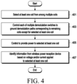
- FIG. 4 is a flowchart illustrating an operation method of an electronic device according to various embodiments.
- the electronic device 101 may select at least one of the plurality of coils 151a,..., 151m in operation 401.
- the electronic device 101 may sequentially apply a ping signal to each of the plurality of coils 151a,..., 151m.
- the electronic device 101 may apply a ping signal to each of the plurality of coils 151a,..., 151m based on a designated order or pattern.
- the electronic device 101 may select at least one coil based on at least one of whether to respond to the ping signal, the SSP identified as the demodulation result, or a change in the voltage or current of the coil, but the criteria for selecting the coil are not limited thereto.
- the electronic device 101 may control each of the plurality of demodulation switches so that the demodulation path corresponding to the coils other than the selected at least one coil are grounded. If the first coil 151a is selected, the electronic device 101 may control the first demodulation switch 152a corresponding to the first coil 151a in an off state and control the remaining demodulation switches corresponding to the other coils than the first coil 151a in an on state. Accordingly, the demodulation path corresponding to the first coil 151a may not be grounded, and the demodulation path corresponding to the remaining coils may be grounded.
- the electronic device 101 may control to supply power to at least one selected coil in operation 405. For example, when the first coil 151a is selected, the electronic device 101 may control the first power conversion circuit 150a to apply power to the first coil 151a. As described below in more detail, the coil selection switch included in the first power conversion circuit 150a or selectively connecting the first power conversion circuit 150a to the transmission IC 110 may be controlled in an on state.
- the electronic device 101 may identify information from the wireless power reception device based on the voltage and/or current applied to at least one selected coil. For example, since the demodulation path corresponding to the remaining coils other than the first coil 151a are grounded, crosstalk between the first coil 151a and the remaining coils may be prevented.
- the electronic device 101 may demodulate the signal of the first coil 151a, that is, the voltage and/or current applied to the first coil 151a.
- the electronic device 101 may identify information from the wireless power reception device based on the demodulation result.
- the information may include at least one of a device ID and an SSP, but the type is not limited.
- the electronic device 101 may control power transmission based on the signal received from the wireless power reception device based on a demodulation result. For example, the electronic device 101 may increase or decrease transmission power or stop power transmission based on the demodulation result.
- FIG. 5 is a view illustrating an operation of grounding a demodulation path corresponding to a coil according to various embodiments.
- a first rectifier 153a and a first demodulation switch 152a may be connected to the first coil 151a. As described above, at least one capacitor may be further connected to the first coil 151a.
- the first demodulation switch 152a may selectively connect a demodulation path corresponding to the first ground 155a and the first coil 151a. When the first demodulation switch 152a is in an on state, the demodulation path corresponding to the first coil 151a and the first ground 155a may be connected. In this case, the signal from the first coil 151a may be applied to the first ground 155a, and no signal may be transferred to the first rectifier 153a.
- first ground 155a is shown as being connected from before the input end of the first rectifier 153a, this is exemplary and, in other implementations, the first demodulation switch 152a and the first ground 155a may be connected from after the output end of the rectifier 153a.
- the demodulation path corresponding to the first coil 151a and the first ground 155a may not be connected.
- the signal from the first coil 151a may be provided to the first rectifier 153a.
- the first rectifier 153a may rectify an input signal.
- the first filter 154a may pass a designated frequency band of the input rectified signal and transfer it to the transmission IC 110. While passing through the first filter 154a, noise of a frequency other than the frequency corresponding to modulation and demodulation of in-band communication may be filtered.
- the transmission IC 110 may demodulate the filtered signal and identify information from the power reception device based on the demodulation result.
- first coil 151a, the first demodulation switch 152a, the first rectifier 153a, the first filter 154a, and the first ground 155a may be equally applied to the second coil 151b, the second demodulation switch 152b, the second rectifier 153b, the second filter 154b, and the second ground 155b and to the Mth coil 151m, the Mth demodulation switch 152m, the Mth rectifier 153m, the Mth filter 154m, and the Mth ground 155m.
- the first rectifier 153a to the Mth rectifier 153m may be implemented as one rectifier or as different pieces of hardware.
- the first filter 154a to the Mth filter 154m may be implemented as one filter or as different pieces of hardware.
- the first ground 155a to the Mth ground 155m may be implemented as a common ground or as different grounds.
- the transmission IC 110 may select any one of the first coil 151a to the Mth coil 151m as a coil for operation.
- the transmission IC 110 may control the demodulation switch corresponding to the selected coil in an off state and control the demodulation switches corresponding to the remaining coils in an on state. Accordingly, as signals from non-selected coils are transferred to the ground, issues with crosstalk in the transmission IC 110 may be alleviated.
- FIG. 6 illustrates a measurement waveform of a voltage according to whether various embodiments apply.
- the electronic device 101 may include a first coil Coil#1 and a second coil Coil#2.
- the first coil Coil#1 and the second coil Coil#2 may be adjacent to each other, for example.
- the first example is an example for comparison with the embodiment.
- the electronic device 101 does not control the demodulation switch corresponding to the first coil Coil#1 and the demodulation switch corresponding to the second coil Coil#2 so that the demodulation switches may be kept in an off state.
- the first waveform 610 may be a voltage sensed from the first coil Coil#1.
- the second waveform 620 is a voltage applied to the first coil Coil#1 and may include, e.g., a ping signal 622.
- the third waveform 630 may be a voltage sensed from the second coil Coil#2.
- the fourth waveform 640 is a voltage applied to the second coil Coil#2 and may include, e.g., a ping signal 641.
- the ping signal 641 may be applied to the second coil Coil#2. Due to the crosstalk, the voltage 611 sensed from the first coil Coil#1 during the first period 601 may be changed.
- the ping signal 622 may be applied to the first coil Coil#1. Due to the crosstalk, the voltage 642 sensed from the second coil Coil#2 during the second period 602 may be changed.
- the second example is an example in which the demodulation switch is manipulated according to the embodiment.
- the fifth waveform 650 may be a voltage sensed from the first coil Coil#1.
- the sixth waveform 660 is a voltage applied to the first coil Coil#1 and may include, e.g., a ping signal 664.
- the seventh waveform 670 may be a voltage sensed from the second coil Coil#2.
- the eighth waveform 680 is a voltage applied to the second coil Coil#2 and may include, e.g., a ping signal 683.
- the demodulation switch corresponding to the second coil Coil#2 may be controlled in an off state, and the demodulation switch corresponding to the first coil Coil#1 may be controlled in an on state.
- the demodulation path corresponding to the first coil Coil#1 may be grounded. Accordingly, the voltage 653 sensed from the first coil Coil#1 may not be affected by the ping signal 683.
- the demodulation switch corresponding to the first coil Coil#1 may be controlled in an off state, and the demodulation switch corresponding to the second coil Coil#2 may be controlled in an on state.
- the demodulation path corresponding to the second coil Coil#2 may be grounded. Accordingly, the voltage 674 sensed from the second coil Coil#2 may not be affected by the ping signal 664.
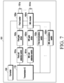
- FIG. 7 is a block diagram illustrating an electronic device capable of wirelessly transmitting power according to various embodiments.
- the electronic device 101 may include at least one of a transmission IC 110, a converter 120, a plurality of coil selection switches 161a,..., 161m, a plurality of gate drivers 162a,..., 162m, a plurality of inverters 163a,..., 163m, a plurality of coils 151a,..., 151m, or a plurality of demodulation switches 152a,..., 152m.
- the first coil selection switch 161a, the first gate driver 162a, and the first inverter 163a may be implemented as a single piece of hardware or may all be implemented as independent pieces of hardware.
- the plurality of coil selection switches 161a,..., 161m may selectively connect the transmission IC 110 to the plurality of gate drivers 162a,..., 162m, respectively.
- the on/off state of each of the plurality of coil selection switches 161a,..., 161m may be controlled by the transmission IC 110.
- the coil selection switches 161a,..., 161m may be implemented as, e.g., level shifters or back-to-back switches.
- the type of coil selection switch is not limited.
- the transmission IC 110 may control the corresponding coil selection switch in an on state so that the selected coil is connected.
- the transmission IC 110 may control the first coil selection switch 161a corresponding to the first coil 151a in an on state.
- the transmission IC 110 may control the remaining coil selection switches in an off state.
- Each of the plurality of gate drivers 162a,..., 162m may apply a driving signal to the gate of the transistor included in each of the plurality of inverters 163a,..., 163m using the received signal.
- the driving signal may be, e.g., in the form of a pulse width modulation (PWM) pulse.
- PWM pulse width modulation
- the inverters 163a,..., 163m may output AC power using the driving voltage (or bridge voltage) from the converter 120 and the driving signal input from each of the gate drivers 162a,..., 162m, For example, when the first coil selection switch 161a is controlled in an on state, the pulse output from the transmission IC 110 may be provided to the first gate driver 162a.
- the first gate driver 162a may apply a driving signal to the gate of the transistor of the first inverter 163a based on the received pulse.
- the first inverter 163a may apply AC power to the first coil 151a according to the driving signal and the driving voltage.
- the transmission IC 110 may control the demodulation switch corresponding to the selected coil in an off state and control the demodulation switch corresponding to the non-selected coil in an on state.
- the first demodulation switch 152a corresponding to the first coil 151a may be controlled in an off state, and the remaining demodulation switches may be controlled in an on state.
- the state of the coil selection switch corresponding to the selected coil and the state of the demodulation switch corresponding to the selected coil may be opposite. Further, the state of the coil selection switch corresponding to the non-selected coil and the state of the demodulation switch corresponding to the non-selected coil may be opposite.
- FIG. 8A is a flowchart illustrating an operation method of an electronic device according to various embodiments.
- the electronic device 101 may select at least one of the plurality of coils 151a,..., 151m in operation 401.
- the electronic device 101 may sequentially apply a ping signal to each of the plurality of coils 151a,..., 151m.
- the electronic device 101 may apply a ping signal to each of the plurality of coils 151a,..., 151m based on a designated order or pattern.
- the electronic device 101 may select at least one coil for power transmission based on at least one of whether to respond to the ping signal, the SSP identified as the demodulation result, or the SSP current, but the criteria for selecting the coil are not limited thereto.
- the electronic device 101 may control the coil selection switch corresponding to at least one selected coil in an on state and control the coil selection switch corresponding to the non-selected coil in an off state.
- the electronic device 101 may control to provide power to at least one selected coil.
- the coil selection switch is controlled in an on state, power may be transferred to the coil through the coil selection switch.
- the electronic device 101 may control the demodulation switch corresponding to the at least one selected coil in an off state and control the demodulation switch corresponding to the non-selected coil in an on state. Accordingly, the demodulation path corresponding to the remaining coils other than the selected at least one coil may be grounded.
- the electronic device 101 may demodulate the signal from the selected coil and identify information from the wireless power reception device based on the demodulation result.
- the transmission IC 110 is connected to the gate driver when the coil selection switch is in an on state, and the transmission IC 110 is not connected to the gate driver when the coil selection switch is in the off state, this is merely an example. According to various embodiments, it will be appreciated by one of ordinary skill in the art that that in an implementation, the transmission IC 110 is connected to the gate driver when the coil selection switch is in an off state, and the transmission IC 110 is not connected to the gate driver when the coil selection switch is in an on state.
- FIG. 8B is a flowchart illustrating an operation method of an electronic device according to various embodiments.
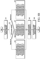
- the electronic device 101 may set the on/off states of a plurality of switches to a default state.
- all of the coil selection switches e.g., the plurality of coil selection switches 161a,..., 161m of FIG. 7
- all of the demodulation switches e.g., the plurality of demodulation switches 152a,..., 152m of FIG. 7
- the electronic device 101 may select a coil for operation. For example, in the embodiment of FIG. 8B , it is assumed that three coils are connected to the electronic device 101, e.g., the transmission IC 110.
- the electronic device 101 may, in operation 815, control the first coil selection switch corresponding to the first coil in an on state, control the second coil selection switch corresponding to the second coil in an off state, and control the third coil selection switch corresponding to the third coil in an off state.
- the electronic device 101 may control the first demodulation switch corresponding to the first coil in an off state, control the second demodulation switch corresponding to the second coil in an on state, and control the third demodulation switch corresponding to the third coil in an on state.
- the electronic device 101 may, in operation 817, control the first coil selection switch in an off state, control the second coil selection switch in an on state, and control the third coil selection switch in an off state.
- the electronic device 101 may control the first demodulation switch in an on state, control the second demodulation switch in an off state, and control the third demodulation switch in an on state.
- the electronic device 101 may, in operation 819, control the first coil selection switch in an off state, control the second coil selection switch in an off state, and control the third coil selection switch in an on state.
- the electronic device 101 may control the first demodulation switch in an on state, control the second demodulation switch in an on state, and control the third demodulation switch in an off state.
- the electronic device 101 may detect termination of the operation associated with the selected coil.
- the electronic device 101 may set the on/off states of the plurality of switches to the default state. If another coil is directly selected, the electronic device 101 may skip the execution of operation 823 and may immediately control the on/off state of the plurality of switches (e.g., coil selection switches and/or demodulation switches) to correspond to the newly selected coil.
- the plurality of switches e.g., coil selection switches and/or demodulation switches
- FIG. 9 is a view illustrating a coil selection switch of an electronic device according to various embodiments.
- the transmission IC 110 may be connected to a plurality of level shifters 901a, 901b, and 901m.
- FIG. 9 illustrates that one output path of the transmission IC 110 is branched to each of the level shifters 901a, 901b, and 901m, but this is exemplary, and three outputs from the transmission IC 110 may be connected to the level shifters 901a, 901b, and 901m, respectively.
- the plurality of level shifters 901a, 901b, and 901m may be connected to gate drivers 162a, 162b, and 162m.
- the transmission IC 110 may output a pulse 911.
- the pulse 911 may be input to the plurality of level shifters 901a, 901b, and 901m.
- the transmission IC 110 may selectively provide a driving voltage Vcc and/or an enable signal En to each of the plurality of level shifters 901a, 901b, and 901m.
- the driving voltage Vcc may be provided from a converter (e.g., the converter 120 of FIG. 7 ).
- the transmission IC 110 may selectively provide the driving voltage Vcc and/or the enable signal En based on a general purpose input/output (GPIO) interface.
- the GPIO is merely an example, and signals may be provided through an interface, such as a serial peripheral interface (SPI) or a mobile industry processor interface (MIPI).
- SPI serial peripheral interface
- MIPI
- the transmission IC 110 may provide the driving voltage Vcc and the enable signal En to the first level shifter 901a.
- the driving voltage Vcc may be provided from the converter 120 as described above.
- the first level shifter 901a may change the level of the input pulse 911 and output the changed pulse 912. For example, when the first level shifter 901a receives a pulse 911 having a level of 3.3V, it may output a pulse 912 having a level of 5V.
- the transmission IC 110 may control not to apply the driving voltage Vcc to the second level shifter 901b or control not to apply the enable signal En.
- the transmission IC 110 may control not to apply the driving voltage Vcc to the third level shifter 901m or control not to apply the enable signal En. Accordingly, the output voltage 913 from the second level shifter 901b and the output voltage 914 from the third level shifter 901m may be substantially zero.
- the first gate driver 162a may receive the level-changed pulse 912.
- the first gate driver 162a may apply a driving signal to the gate of the transistor of the first inverter 163a using the pulse 912.
- the first inverter 163a may output AC power 915 using the driving signal applied to the gate of the transistor and the DC voltage Vbrdige input from the converter 120.
- the first inverter 163a may output power based on the DC voltage Vbridge while the driving signal applied to the gate of the transistor is on duration.
- the first inverter 163a may not output power based on the DC voltage Vbridge while the driving signal applied to the gate of the transistor is off duration. Accordingly, AC power 915 may be applied to the first coil 151a.
- the gate drivers 162b and 162m may not operate so that AC power may not be provided to the second coil 151b and the mth coil 151m.
- the gate may be grounded and, as all of the power conversion circuits (e.g., gate drivers and/or inverters) are connected to ground, interference may be reduced.
- whether AC power is provided to the coil may be determined depending on whether signals are output from the level shifters 901a, 901b, and 901m. Since the level shifters 901a, 901b, and 901m may be controlled by the on/off scheme of the DC power, isolation between the level shifters 901a, 901b, and 901m is possible, and the AC switch may be prevented from application of a high internal pressure.
- the switch for providing power to the selected coil may be included not only in an electronic device 101 using in-band communication as shown in FIG. 3 or 7 but also in an electronic device (e.g., an electronic device according to the AFA standard) using out-of-band communication.
- FIG. 10A is a block diagram illustrating an electronic device according to various embodiments. The embodiment of FIG. 10A is described with reference to FIG. 10B.
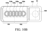
- FIG. 10B is a concept view illustrating an electronic device according to various embodiments.
- the electronic device 101 may include a first transmission IC 1012, a second transmission IC 1022, and a third transmission IC 1032.
- the first transmission IC 1012 may provide a signal (e.g., a ping signal or a signal for charging) to the first coil 1016a, the second coil 1016b, and the third coil 1016c.
- the first transmission IC 1012 may demodulate signals output from the first coil 1016a, the second coil 1016b, and the third coil 1016c and identify information from the wireless power reception device based on the demodulation result. For example, as shown in FIG.
- the second transmission IC 1022 may provide a signal (e.g., a ping signal or a signal for charging) to the fourth coil 1026a, the fifth coil 1026b, and the sixth coil 1026c.
- the second transmission IC 1022 may demodulate signals output from the fourth coil 1026a, the fifth coil 1026b, and the sixth coil 1026c and identify information from the wireless power reception device based on the demodulation result. For example, as shown in FIG.
- the fourth coil 1026a, the fifth coil 1026b, and the sixth coil 1026c may be disposed to cover the second area 1042 of the electronic device 101.
- the third transmission IC 1032 may provide a signal (e.g., a ping signal or a signal for charging) to the seventh coil 1036.
- the third transmission IC 1032 may demodulate the signal output from the seventh coil 1036 and identify information from the wireless power reception device based on the demodulation result.
- the seventh coil 1036 may be disposed to cover the third area 1043 of the electronic device 101.
- the electronic device 101 has three areas 1041, 1042, and 1043 and/or seven coils 1016a, 1016b, 1016c, 1026a, 1026b, 1026c, and 1036, and there is no limitation on the areas and/or the number, position, size or shape of the coils.
- the first coil selection switch 1013a, the second coil selection switch 1013b, and the third coil selection switch 1013c may selectively connect the first transmission IC 1012 to the first gate driver 1014a, the second gate driver 1014b, and the third gate driver 1014c, respectively.
- Each of the first coil selection switch 1013a, the second coil selection switch 1013b, and the third coil selection switch 1013c may be implemented as, e.g., a level shifter, but the implementation form is not limited.
- the on/off state of each of the first coil selection switch 1013a, the second coil selection switch 1013b, and the third coil selection switch 1013c may be controlled by the first transmission IC 1012.
- the first gate driver 1014a, the second gate driver 1014b, and the third gate driver 1014c may apply driving signals to the gates of the first inverter 1015a, the second inverter 1015b, and the third inverter 1015c, respectively, using the pulse received from the transmission IC 1012 (or the pulse whose level has been changed by the level shifter).
- Each of the first inverter 1015a, the second inverter 1015b, and the third inverter 1015c may provide AC power to the first coil 1016a, the second coil 1016b, and the third coil 1016c, respectively, using the driving voltage from the first converter 1011 and the driving signals received from the gate drivers 1014a, 1014b, and 1014c.
- the first demodulation switch 1017a, the second demodulation switch 1017b, and the third demodulation switch 1017c may selectively ground the first inverter 1015a, the second inverter 1015b, and the third inverter 1015c, respectively.
- the first inverter 1015a, the second inverter 1015b, and the third inverters 1015c may be connected to ground.
- the first inverter 1015a, the second inverter 1015b, and the third inverter 1015c each may not be connected to ground.
- the first filter 1018 may pass a designated frequency band of the input signal (e.g., a rectified signal) and transfer the signal to the first transmission IC 1012.
- the first filter 1018 may pass a designated frequency band of the signal input from a demodulation switch, which is in an off state, among the first demodulation switch 1017a, the second demodulation switch 1017b, and the third demodulation switch 1017c and transfer it to the first transmission IC 1012.
- a single first filter may be configured and connected to a plurality of demodulation switches or a plurality of first filters 1018 may be configured and connected to a plurality of demodulation switches, respectively.
- the first transmission IC 1012 may demodulate the filtered signal and identify information based on the demodulation result.
- the fourth coil selection switch 1023a, the fifth coil selection switch 1023b, and the sixth coil selection switch 1023c may selectively connect the second transmission IC 1022 to the fourth gate driver 1024a, the fifth gate driver 1024b, and the sixth gate driver 1024c, respectively.
- Each of the fourth coil selection switch 1023a, the fifth coil selection switch 1023b, and the sixth coil selection switch 1023c may be implemented as, e.g., a level shifter, but the implementation form is not limited.
- the on/off state of each of the fourth coil selection switch 1023a, the fifth coil selection switch 1023b, and the sixth coil selection switch 1023c may be controlled by the second transmission IC 1022.
- the fourth gate driver 1024a, the fifth gate driver 1024b, and the sixth gate driver 1024c may apply driving signals to the gates of the fourth inverter 1025a, the fifth inverter 1025b, and the sixth inverter 1025c, respectively, using the pulse received from the second transmission IC 1022 (or the pulse whose level has been changed by the level shifter).
- Each of the fourth inverter 1025a, the fifth inverter 1025b, and the sixth inverter 1025c may provide AC power to the fourth coil 1026a, the fifth coil 1026b, and the sixth coil 1026c, respectively, using the driving voltage from the second converter 1021 and the driving signals received from the gate drivers 1024a, 1024b, and 1024c.
- the fourth demodulation switch 1027a, the fifth demodulation switch 1027b, and the sixth demodulation switch 1027c may selectively ground the fourth inverter 1025a, the fifth inverter 1025b, and the sixth inverter 1025c, respectively.
- the fourth inverter 1025a, the fifth inverter 1025b, and the sixth inverters 1025c may be connected to ground.
- the fourth inverter 1025a, the fifth inverter 1025b, and the sixth inverter 1025c each may not be connected to ground.
- the second filter 1028 may pass a designated frequency band of the input signal (e.g., a rectified signal) and transfer the signal to the second transmission IC 1022.
- the second filter 1028 may pass a designated frequency band of the signal input from a demodulation switch, which is in an off state, among the fourth demodulation switch 1027a, the fifth demodulation switch 1027b, and the sixth demodulation switch 1027c and transfer it to the second transmission IC 1022.
- a single second filter may be configured and connected to a plurality of demodulation switches or a plurality of second filters 1028 may be configured and connected to a plurality of demodulation switches, respectively.
- the second transmission IC 1022 may demodulate the filtered signal and identify information based on the demodulation result.
- the seventh gate driver 1034 may apply the driving signal to the gate of the transistor of the seventh inverter 1035 using the pulse received from the third transmission IC 1032 (or the pulse whose level has been changed by the level shifter).
- the seventh inverter 1035 may provide AC power to the seventh coil 1036 based on the driving signal received from the seventh gate driver 1034 and the driving voltage from the third converter 1031.
- the number of three transmission ICs 1012, 1022, and 1032 is merely exemplary but is not limited.
- the MCU 1005 may transmit/receive data to/from the transmission ICs 1012, 1022, and 1032.
- the MCU 1005 may receive data from the transmission ICs 1012, 1022, and 1032 and may transmit data for controlling the transmission ICs 1012, 1022, and 1032.
- the first transmission IC 1012 may select any one of the first coil 1016a, the second coil 1016b, and the third coil 1016c and apply power (e.g., a ping signal) to the selected coil.
- the second transmission IC 1022 may select any one of the fourth coil 1026a, the fifth coil 1026b, and the sixth coil 1026c and apply power (e.g., a ping signal) to the selected coil.
- the MCU 1005 may transmit a control command to output a ping signal to the plurality of transmission ICs 1012, 1022, and 1032 and thus be controlled not to simultaneously apply ping signals to the plurality of coils.
- the MCU 1005 is not limited as long as it is hardware capable of calculation, and may be referred to as a processor.
- the USB socket 1001 may be a socket into which a USB-type connecting terminal may be inserted.
- the over-voltage protection (OVP) circuit 1003 may perform an operation to protect hardware within the electronic device 101 when an overvoltage is applied from the outside.
- the regulator 1007 may be, e.g., a low drop output (LDO) regulator.
- the temperature sensor 1009 may measure the temperature of at least one point within the electronic device 101 and, based on the temperature, the MCU 1005 may also perform an over temperature protection operation.
- FIG. 11A is a flowchart illustrating an operation method of an electronic device according to various embodiments.
- the electronic device 101 may perform ping signal application and information identification on each of the plurality of coils based on a designated order. For example, the electronic device 101 may control to apply a ping signal to each of the plurality of coils 1016a, 1016b, 1016c, 1026a, 1026b, 1026c, and 1036, sequentially or in a designated pattern.
- the electronic device 101 may control the first transmission IC 1012 to apply a ping signal to the first coil 1016a and may control the second transmission IC 1022 to apply a ping signal to the fourth coil 1026a if the application of the ping signal to the first coil 1016a is finished. In one example, the electronic device 101 may control the transmission ICs 1012 and 1022 to apply ping signals in the order of the first coil 1016a, the fourth coil 1026a, the second coil 1016b, the fifth coil 1026b, the third coil 1016c, and the sixth coil 1026c, but the order is not limited.
- the electronic device 101 may control the transmission ICs 1012 and 1022 to apply ping signals in the order of the third coil 1016c, the fourth coil 1026a, the second coil 1016b, the fifth coil 1026b, the first coil 1016a, and the sixth coil 1026c.
- the electronic device 101 may identify information from each of the plurality of coils while applying the ping signal.
- the wireless power reception device may receive the ping signal and transmit information about the SSP in response to the ping signal.
- the wireless power reception device may perform on/off keying modulation based on the information about the SSP.
- the electronic device 101 may identify the SSP corresponding to a specific coil based on a demodulation result of current and/or voltage applied to the specific coil.
- the electronic device 101 may identify the SSP corresponding to each of the plurality of coils.
- the SSP may be identified for the coil where a wireless power reception device is disposed, but the SSP may not be identified for the coil where a wireless power reception device is not disposed.
- the electronic device 101 fails in demodulation because on/off keying modulation is not performed.
- the electronic device 101 may select at least one coil to perform an operation based on a comparison result of information from each of the plurality of coils. For example, the electronic device 101 may select the coil corresponding to the highest SSP. The electronic device 101 may determine that a wireless power reception device is disposed on the coil selected based on the highest SSP. The electronic device 101 may perform a subsequent operation (e.g., an authentication procedure, a power transmission procedure) on the selected coil.
- a subsequent operation e.g., an authentication procedure, a power transmission procedure
- FIG. 11B is a flowchart illustrating an operation method of an electronic device according to various embodiments.
- the electronic device 101 may apply a ping signal to the coil and identify information (e.g., SSP) while applying the ping signal.
- the first coil may be set according to a designated order.
- the electronic device 101 may determine whether there is the next coil.
- the electronic device 101 may determine whether there is a coil to be measured by applying a ping signal after the coil for which measurement is currently performed based on the designated order. If the next coil is present (yes in 1113), the electronic device 101 may change the coil to be measured in operation 1115.
- the electronic device 101 may identify the next coil to be measured based on the designated order.
- the electronic device 101 may repeat operations of changing a coil, applying a ping signal, and identifying information until there is no next coil (no in 1113).
- the electronic device 101 may select a coil according to comparison of information about each of the plurality of coils in operation 1117.
- FIG. 11C is a flowchart illustrating an operation method of an electronic device according to various embodiments.
- the electronic device 101 may perform ping signal application, information identification and current measurement, e.g., SSP current measurement, on each of the plurality of coils based on a designated order. While the ping signal is applied to any one coil, the electronic device 101 may identify the SSP based on a demodulation result and measure the magnitude of the current applied to the coil. As described above, the SSP current may be related to alignment between the coils.
- the SSP current value in the first coil 1016a is a first value
- the SSP current value in the second coil 1016b is a second value.
- the first value being smaller than the second value may mean that the first coil 1016a is better aligned with the coil of the wireless power reception device than the second coil 101b.
- the SSP current value being 0 may mean that a wireless power reception device is not disposed on the corresponding coil.
- the electronic device 101 may execute at least one coil to perform an operation based on a comparison result of information from each of the plurality of coils and a result of measurement of current at each of the plurality of coils. For example, the electronic device 101 may identify information and measurement results as shown in Table 1. [Table 1] coil #1 #2 #3 #4 #5 #6 SSP 0 0 80 120 60 0 SSP current(mA) 0 0 170 150 200 0
- the SSP current may mean the magnitude of current measured at the corresponding coil while a signal including the SSP is received.
- the magnitude being 0 may mean, e.g., that demodulation of the signal including the SSP fails, so that the magnitude of the corresponding current is not measured or recorded.
- the wireless power reception device when the wireless power reception device is disposed over the third coil 1016c, the fourth coil 1026a, and the fifth coil 1026b of the electronic device 101, demodulation results corresponding to the third coil 1016c, the fourth coil 1026a and the fifth coil 1026b may be identified.
- the electronic device 101 may identify the SSPs (e.g., 80, 120, and 60) respectively corresponding to the third coil 1016c, the fourth coil 1026a, and the fifth coil 1026b, based on the demodulation results corresponding to the third coil 1016c, the fourth coil 1026a, and the fifth coil 1026b.
- the electronic device 101 may identify SSP currents (e.g., 170 mA, 150 mA, and 200 mA) corresponding to the third coil 1016c, the fourth coil 1026a, and the fifth coil 1026b.
- the electronic device 101 may select the fourth coil 1026a corresponding to the highest SSP.
- the electronic device 101 may select the fourth coil 1026a corresponding to the lowest SSP current among values other than 0.
- the electronic device 101 may select the fourth coil 1026a considering both the SSP and the SSP current.
- the electronic device 101 may assign weights to SSP and SSP current and select one coil based on the assigned weights. Meanwhile, there are no limitation on the parameters for selecting the coil other than SSP and SSP current.
- the electronic device 101 may perform ping signal application, information identification, and current measurement on any one coil and change to the next coil based on the designated order. If information identification and current measurement are completed up to the last coil, the electronic device 101 may select a coil based on the identified information and the measured current.
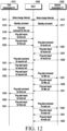
- FIG. 12 is a flowchart illustrating an operation method of an electronic device according to various embodiments.
- the MCU 1005 may receive a mode change interrupt from the first transmission IC 1012 in operation 1211.
- the MCU 1005 may receive a mode change interrupt from the second transmission IC 1022 in operation 1213.
- the first transmission IC 1012 and the second transmission IC 1022 may transmit the mode change interrupt to the MCU 1005 when preparation for performing a ping procedure is completed.
- the MCU 1005 may provide a standby command to the first transmission IC 1012 in response to the received mode change interrupt in operation 1215.
- the MCU 1005 may provide a standby command to the second transmission IC 1022 in response to the received mode change interrupt in operation 1217.
- the standby command may be a command to prepare for a ping signal application operation.
- the standby command may allow the transmission ICs 1012 and 1022 to set the on/off states of the plurality of switches to the default state.
- the first transmission IC 1012 may control the first coil selection switch 1013a, the second coil selection switch 1013b, and the third coil selection switch 1013c in an off state and control the first demodulation switch 1017a, the second demodulation switch 1017b and the third demodulation switch 1017c in an on state.
- the second transmission IC 1022 may control the fourth coil selection switch 1023a, the fifth coil selection switch 1023b, and the sixth coil selection switch 1023c in an off state and control the fourth demodulation switch 1027a, the fifth demodulation switch 1027b and the sixth demodulation switch 1027c in an on state.
- the MCU 1005 may provide a standby command and may provide commands to the first transmission IC 1012 and the second transmission IC 1022 to sequentially apply a ping signal to each of the plurality of coils.
- an order of transmission of ping signals may be stored in a memory (not shown) of the electronic device 101.
- the MCU 1005 may load the transfer the order from the memory (not shown).
- the transmission order may be a designated order or an order based on the user's use pattern. In the embodiment of FIG.
- ping signals may be set to be applied in the order of the first coil 1016a, the fourth coil 1026a, the second coil 1016b, the fifth coil 1026b, the third coil 1016c, and the sixth coil 1026c.
- the MCU 1005 may transmit a ping start command to the first coil 1016a in operation 1219.
- the first transmission IC 1012 may control to apply a ping signal to the first coil 1016a based on the ping start command.
- the first transmission IC 1012 may control the first coil selection switch 1013a in FIG. 10A in an on state and control the second coil selection switch 1013b and the third coil selection switch 1013c in an off state.
- the first transmission IC 1012 may control the first demodulation switch 1017a in an off state and control the second demodulation switch 1017b and the third demodulation switch 1017c in an on state while demodulating the signal provided through the first demodulation switch 1017a.
- the first transmission IC 1012 may control to apply the ping signal to the first coil 1016a for a first period (e.g., 88 ms).
- the first transmission IC 1012 may report the start of ping for the first coil 1016a to the MCU 1005 in operation 1221.
- the first transmission IC 1012 may report the end of ping for the first coil 1016a to the MCU 1005 in operation 1223.
- the MCU 1005 may identify that the ping procedure for the first coil 1016a is ended, based on the report of the start of the ping in operation 1221 and the report of the end of the ping in operation 1223.
- the first transmission IC 1012 may set the on/off state of the plurality of switches 1013a, 1013b, 1013c, 1017a, 1017b, and 1017c to the default state when the ping procedure for the first coil 1016a is ended. Thereafter, the MCU 1005 may provide a ping start command for the fourth coil 1026a to the second transmission IC 1022 in operation 1225.
- a period of, e.g., 200 ms may be provided between the timing of the ping start command for the first coil 1016a in operation 1219 and the timing of the ping start command for the fourth coil 1026a in operation 1225, but is not limited thereto. Accordingly, while the ping signal is applied to the first coil 1016a, no ping signal may be applied to the other coils.
- the MCU 1005 may transmit a ping start command to the fourth coil 1026a in operation 1225.
- the second transmission IC 1022 may control to apply a ping signal to the fourth coil 1026a based on the ping start command.
- the second transmission IC 1022 may control the fourth coil selection switch 1023a in FIG. 10A in an on state and control the fifth coil selection switch 1023b and the sixth coil selection switch 1023c in an off state.
- the second transmission IC 1022 may control the fourth demodulation switch 1027a in an off state and control the fifth demodulation switch 1027b and the sixth demodulation switch 1027c in an on state while demodulating the signal provided through the fourth demodulation switch 1027a.
- the second transmission IC 1022 may control to apply the ping signal to the fourth coil 1026a for the first period (e.g., 88 ms).
- the second transmission IC 1022 may report the start of ping for the fourth coil 1026a to the MCU 1005 in operation 1227.
- the second transmission IC 1022 may report the end of ping for the fourth coil 1026a to the MCU 1005 in operation 1229.
- the MCU 1005 may identify that the ping procedure for the fourth coil 1026a is ended, based on the report of the start of the ping in operation 1227 and the report of the end of the ping in operation 1229.
- the MCU 1005 may control the ping procedure to be sequentially performed on the second coil 1016b, the fifth coil 1026b, the third coil 1016c, and the sixth coil 1026c according to the set order, Operations 1231, 1233, and 1235 may be substantially the same as operations 1219, 1221, and 1223 except that the coil to which the ping signal is applied is the second coil 1016b.
- the first transmission IC 1012 may control the states of switches corresponding to the second coil 1016b. For example, the first transmission IC 1012 may control the first coil selection switch 1013b in an on state and control the first coil selection switch 1013a and the third coil selection switch 1013c in an off state.
- the first transmission IC 1012 may control the second demodulation switch 1017b in an off state and control the first demodulation switch 1017a and the third demodulation switch 1017c in an on state.
- Operations 1237, 1239, and 1241 may be substantially the same as operations 1225, 1227, and 1229 except that the coil to which the ping signal is applied is the fifth coil 1026b.
- the second transmission IC 1022 may control the states of switches corresponding to the fifth coil 1026b.
- the second transmission IC 1022 may control the fifth coil selection switch 1023b in an on state and control the fourth coil selection switch 1023a and the sixth coil selection switch 1023c in an off state.
- the second transmission IC 1022 may control the fifth demodulation switch 1027b in an off state and control the fourth demodulation switch 1027a and the sixth demodulation switch 1027c in an on state.
- Operations 1243, 1245, and 1247 may be substantially the same as operations 1219, 1221, and 1223 except that the coil to which the ping signal is applied is the third coil 1016c.
- the first transmission IC 1012 may control the states of switches corresponding to the third coil 1016c. For example, the first transmission IC 1012 may control the third coil selection switch 1013c in an on state and control the first coil selection switch 1013a and the second coil selection switch 1013b in an off state.
- the first transmission IC 1012 may control the third demodulation switch 1017c in an off state and control the first demodulation switch 1017a and the second demodulation switch 1017b in an on state.
- Operations 1249, 1251, and 1253 may be substantially the same as operations 1225, 1227, and 1229 except that the coil to which the ping signal is applied is the sixth coil 1026c.
- the second transmission IC 1022 may control the states of switches corresponding to the sixth coil 1026c.
- the second transmission IC 1022 may control the sixth coil selection switch 1023c in an on state and control the fourth coil selection switch 1023a and the fifth coil selection switch 1023c in an off state.
- the second transmission IC 1022 may control the sixth demodulation switch 1027c in an off state and control the fourth demodulation switch 1027a and the fifth demodulation switch 1027b in an on state.
- the MCU 1005 may repeat the ping procedure according to a designated order.
- the MCU 1005 may repeat the ping procedure according to a fixed order or may change the ping procedure execution order each time it is performed.
- FIG. 13 is a flowchart illustrating an operation method of an electronic device according to various embodiments.
- the first transmission IC 1012 may perform a ping procedure on a plurality of coils. For example, as shown in FIG. 12 , the first transmission IC 1012 may apply a ping signal to each of a plurality of coils associated with the first transmission IC 1012, based on a ping start command for a specific coil from the MCU 1005. In operation 1303, the first transmission IC 1012 may identify information from each of the plurality of coils. In operation 1305, the first transmission IC 1012 may measure current at each of the plurality of coils. Information identification and current measurement for each of the plurality of coils may be sequentially performed for each coil.
- the first transmission IC 1012 may select one of the plurality of coils based on at least one of identified information or measured current.
- the second transmission IC 1022 may also perform operations 1301, 1303, 1305, and 1307.
- the MCU 1005 may control the first transmission IC 1012 and the second transmission IC 1022 so that ping signals are not simultaneously applied to the plurality of coils.
- the first transmission IC 1012 may transmit a charge preparation request to the MCU 1005 in operation 1309.
- the charge preparation request may include information (e.g., coil identification information) indicating the coil selected by the first transmission IC 1012, for example.
- the MCU 1005 may transmit a charge preparation command to the first transmission IC 1012 based on the reception of the charge preparation request.
- the MCU 1005 may read or access the value stored for the first transmission IC 1012.
- the first transmission IC 1012 may store information associated with the selected coil (e.g., SSP and/or SSP current). The MCU 1005 may read the stored information.
- the MCU 1005 may transmit a power transfer command to the first transmission IC 1012 based on the stored information. If the MCU 1005 receives the charge preparation request only from the first transmission IC 1012, the MCU 1005 may transmit a power transfer command for the coil selected by the first transmission IC 1012. For example, when SSP and SSP current are selected only for the first coil 1016a and the second coil 1016b, only the first transmission IC 1012 may transmit a charge preparation request, and the second transmission IC 1022 that has not performed any measurement may not transmit a charge preparation request.
- the MCU 1005 may transmit a power transfer command for the coil selected by the second transmission IC 1022. If the MCU 1005 receives charge preparation requests from both the first transmission IC 1012 and the second transmission IC 1022, the MCU 1005 may compare the values read from both the transmission ICs 1012 and 1022. The MCU 1005 may select a coil based on the comparison result. The MCU 1005 may transmit a power transfer command for the selected coil to the transmission IC corresponding to the selected coil, which is described with reference to FIGS. 15A, 15B and 15C .
- the MCU 1005 may transmit power transfer commands to both the first transmission IC 1012 and the second transmission IC 1022. If the first transmission IC 1012 may select the first coil 1016a, and the second transmission IC 1022 selects the sixth coil 1026c, the MCU 1005 may transmit power transfer commands to all of the one or more transmission ICs 1012 and 1022 so that all of the selected coils perform charging. In one example, when it is determined that the coil selected by the first transmission IC 1012 and the coil selected by the second transmission IC 1022 are spaced apart by a designated distance or more, the MCU 1005 may determine to perform charging on both the coils.
- the MCU 1005 may determine to perform charging on both the coils and transmit power transfer commands to all of the one or more transmission ICs 1012 and 1022.
- FIG. 14 is a flowchart illustrating an operation method of an electronic device according to various embodiments.
- Operations 1401, 1403, and 1405 may be substantially the same as operations 1301, 1303, and 1305 of FIG. 13 and, thus, a description thereof will be omitted.
- the first transmission IC 1012 may select one of the plurality of coils based on at least one of identified information or measured current and initiate charging. As compared to the embodiment of FIG. 13 , the first transmission IC 1012 may directly start power transmission without a separate power transfer command from the MCU 1005. In operation 1409, the first transmission IC 1012 may notify the MCU 1005 of power transmission. In one example, the first transmission IC 1012 may initiate charging on the selected coil without any particular condition determination and may notify the MCU 1005 of power transmission. For example, the first transmission IC 1012 may start charging the selected coil without determining any particular conditions.
- the first transmission IC 1012 may determine whether a power transmission condition is met and, upon determining that the power transmission condition is met, initiate charging of the selected coil and notify the MCU 1005 of power transmission.
- the power transmission condition may be that the coil selected by the first transmission IC 1012 may be one selected from the remaining coils (e.g., the first coil 1016a and the second coil 1016b) other than the coil (e.g., the third coil 1016c) disposed in a position adjacent to one of the coils controlled by the second transmission IC 1022, but is not limited thereto.
- the first transmission IC 1012 may transmit a charge preparation request to the MCU 1006 and, upon receiving a power transfer command from the MCU 1006, initiate charging as shown in FIG. 13 .
- FIG. 15A illustrates an example of mounting a wireless power reception device on a plurality of coils according to various embodiments.
- FIG. 15B illustrates an example of mounting a wireless power reception device on a plurality of coils according to various embodiments.
- FIG. 15C illustrates an example of mounting a wireless power reception device on a plurality of coils according to various embodiments.
- the embodiment of FIGS. 15A to 15C is described with reference to FIGS. 16A and 16B .
- FIGS. 16A and 16B are flowcharts illustrating a method for operating an electronic device according to an embodiment. Operations 1401, 1403, and 1405 may be substantially the same as operations 1301, 1303, and 1305 of FIG. 13 and, thus, a description thereof will be omitted.
- the electronic device 101 may include a plurality of coils 1016a, 1016b, 1016c, 1026a, 1026b, and 1026c.
- the wireless power reception device 1500 may be mounted on the third coil 1016c, the fourth coil 1026a, and the fifth coil 1026b.
- the MCU 1005 may transmit a ping start command for the first coil 1016a to the first transmission IC 1012 in operation 1601.
- the first transmission IC 1012 may apply a ping signal to the first coil 1016a.
- the first transmission IC 1012 may report the ping signal start for the first coil 1016a to the MCU 1005 in operation 1603 and report the end of the ping for the first coil 1016a to the MCU 1005 in operation 1605. Although the ping signal is applied to the first coil 1016a, since the wireless power reception device 1500 is not mounted on the first coil 1016a, the first transmission IC 1012 may fail to detect demodulation by the wireless power reception device 1500 corresponding to the ping signal.
- the MCU 1005 may transmit a ping start command for the fourth coil 1026a to the second transmission IC 1022 in operation 1607.
- the second transmission IC 1022 may apply a ping signal 1511 to the fourth coil 1026a.
- the second transmission IC 1022 may report the ping signal start for the fourth coil 1026a to the MCU 1005 in operation 1603.
- the second transmission IC 1022 may identify information about the fourth coil 1026a.
- the second transmission IC 1022 may identify information indicating that the SSP of the fourth coil 1026a is 120 and the SSP current is 150 mA.
- the second transmission IC 1022 may report the end of ping for the fourth coil 1026a to the MCU 1005 in operation 1613.
- the MCU 1005 may transmit a ping start command for the second coil 1016b to the first transmission IC 1012 in operation 1615.
- the first transmission IC 1012 may apply a ping signal to the second coil 1016b.
- the first transmission IC 1012 may report the ping signal start for the second coil 1016b to the MCU 1005 in operation 1617 and report the end of the ping for the second coil 1016b to the MCU 1005 in operation 1619.
- the ping signal is applied to the second coil 1016b, since the wireless power reception device 1500 is not mounted on the second coil 1016b, the first transmission IC 1012 may fail to detect demodulation by the wireless power reception device 1500 corresponding to the ping signal.
- the MCU 1005 may transmit a ping start command for the fifth coil 1026b to the second transmission IC 1022 in operation 1621.
- the second transmission IC 1022 may apply a ping signal 1512 to the fifth coil 1026b.
- the second transmission IC 1022 may report the ping signal start for the fifth coil 1026b to the MCU 1005 in operation 1623.
- the second transmission IC 1022 may identify information about the fifth coil 1026b.
- the second transmission IC 1022 may identify information indicating that the SSP of the fifth coil 1026b is 60 and the SSP current is 200 mA.
- the second transmission IC 1022 may report the end of ping for the fifth coil 1026b to the MCU 1005 in operation 1627.
- the MCU 1005 may transmit a ping start command for the third coil 1016c to the first transmission IC 1012 in operation 1629.
- the first transmission IC 1012 may apply a ping signal 1513 to the third coil 1016c.
- the first transmission IC 1012 may report the ping signal start for the third coil 1016c to the MCU 1005 in operation 1631.
- the first transmission IC 1012 may identify information about the third coil 1016c.
- the first transmission IC 1022 may identify information indicating that the SSP of the third coil 1016c is 80 and the SSP current is 170 mA.
- the first transmission IC 1012 may report the end of ping for the third coil 1016c to the MCU 1005 in operation 1635.
- the MCU 1005 may transmit a ping start command for the sixth coil 1026c to the second transmission IC 1022 in operation 1637.
- the second transmission IC 1022 may apply a ping signal to the sixth coil 1026c.
- the second transmission IC 1022 may report the ping signal start for the sixth coil 1026c to the MCU 1005 in operation 1639 and identify information about the sixth coil 1026c in operation 1641.
- the second transmission IC 1022 may identify an SSP of 0 and an SSP current of 0.
- the second transmission IC 1022 may identify the SSP and SSP current based on identifying that the SSP and SSP current for the fourth coil 1026a and the fifth coil 1026b are identified and identify and/or record the values. If information is identified from none of the coils before measuring a specific coil, i.e., if demodulation fails, the electronic device 101 may not identify and/or record the measurement result on a previous coil and specific coil.
- the second transmission IC 1022 may report the end of ping for the sixth coil 1026c to the MCU 1005 in operation 1643.
- the second transmission IC 1022 may select one coil to perform power transmission to the wireless power reception device 1500 based on information about each of the coils 1026a, 1026b, and 1026c.
- the second transmission IC 1022 may report information about the selected coil.
- the second transmission IC 1022 may select the fourth coil 1026a based on the SSP and the SSP current and may report information indicating the fourth coil 1026a to the MCU 1005.
- FIGS. 16A and 16B illustrate that the second transmission IC 1022 reports a ping end report in operation 1643 and reports information about the selected coil to the MCU 1005 in operation 1647, this is exemplary.
- the second transmission IC 1022 may omit the ping end report on the last coil after terminating the information identification on all of the coils 1026a, 1026b, and 1026c and transmit information about the selected coil to the MCU 1005.
- the MCU 1005 may determine that ping application for the coil to which the ping signal is applied is terminated. In operation 1649, the MCU 1005 may transmit a power transmission preparation command to the second transmission IC 1022.
- the MCU 1005 may read information about the selected coil. For example, the MCU 1005 may read SSP: 120 and SSP current: 150 mA for the fourth coil 1026a, which is the selected coil.
- the MCU 1005 may transmit a ping start command for the first coil 1026c to the first transmission IC 1012 in operation 1653. Since the MCU 1005 has not received information about the selected coil from the first transmission IC 1012, the MCU 1005 may be implemented to transmit a ping start command to the first transmission IC 1012. For example, in FIG. 16B , the first transmission IC 1012 may initially identify the SSP and SSP current and then perform the identification procedure on unidentified coils and then select one coil. However, this is merely an example, and the first transmission IC 1012 may select a coil if a ping procedure for the last coil in order is terminated.
- the first transmission IC 1012 may apply a ping signal to the first coil 1026a.
- the first transmission IC 1012 may report the ping signal start for the first coil 1016a to the MCU 1005 in operation 1655 and identify information about the first coil 1016a in operation 1657.
- the first transmission IC 1012 may identify the SSP of 0 and the SSP current of 0 and record the identification result to the first transmission IC 1012.
- the first transmission IC 1012 may record information about the SSP and SSP current corresponding to the third coil 1026c based on identifying the SSP based on success in demodulation for the third coil 1026c.
- the first transmission IC 1012 may be configured to update the information whenever a ping procedure is performed.
- the second transmission IC 1012 may report the end of ping for the first coil 1016a to the MCU 1005 in operation 1659.
- the MCU 1005 may provide a ping start command for the second coil 1016b to the first transmission IC 1012 in operation 1661.
- the first transmission IC 1012 may apply a ping signal to the second coil 1026b.
- the first transmission IC 1012 may report the ping signal start for the second coil 1016b to the MCU 1005 in operation 1663 and identify information about the second coil 1016b in operation 1665. However, since the wireless power reception device is not mounted on the second coil 1016b, the first transmission IC 1012 may identify the SSP of 0 and the SSP current of 0. The first transmission IC 1012 may report the end of ping for the second coil 1016b to the MCU 1005 in operation 1667. The first transmission IC 1012 may select any one coil based on the identified information (e.g., SSP and SSP current).
- the identified information e.g., SSP and SSP current
- the first transmission IC 1012 may report information about the selected coil.
- the first transmission IC 1012 may select the third coil 1016c based on the SSP and the SSP current and may report information indicating the third coil 1016c to the MCU 1005.
- FIGS. 16A and 16B illustrate that the first transmission IC 1012 reports a ping end report in operation 1667 and reports information about the selected coil to the MCU 1005 in operation 1671, this is exemplary.
- the first transmission IC 1012 may omit the ping end report on the last coil after terminating the information identification on all of the coils 1016a, 1016b, and 1016c and transmit information about the selected coil to the MCU 1005.
- the MCU 1005 may determine that ping application for the coil to which the ping signal is applied is terminated. In operation 1673, the MCU 1005 may transmit a power transmission preparation command to the first transmission IC 1012.
- the MCU 1005 may read information about the selected coil. For example, the MCU 1005 may read SSP: 80 and SSP current: 170 mA for the third coil 1016c, which is the selected coil.
- the MCU 1005 may compare the information read in operation 1677 to select a coil for power transmission. For example, the MCU 1005 may compare SSP: 80, SSP current: 170mA for the third coil 1016c, read from the first transmission IC 1012, and SSP: 120, SSP current: 150mA for the fourth coil 1026a, read from the second transmission IC 1022. Based on the comparison result, the MCU 1005 may select, e.g., the fourth coil 1026a. In operation 1679, the MCU 1005 may transmit a power transfer command using the selected coil (e.g., the fourth coil 1026a) to the transmission IC (e.g., the second transmission IC 1022) corresponding to the selected coil.
- the selected coil e.g., the fourth coil 1026a
- the transmission IC e.g., the second transmission IC 1022
- the second transmission IC 1022 that has received the power transfer command may transmit power through the selected coil (e.g., the fourth coil 1026a).
- the MCU 1005 may command to transmit power through a plurality of coils based on the information about the selected coil, read from the second transmission IC 1022 through operation 1651, and the information about the selected coil, read from the first transmission IC 1021 through operation 1675. For example, when the plurality of wireless power reception devices meet a designated condition for receiving wireless power from the electronic device 101, the MCU 1005 may transmit a power transfer command using the selected coil, to each of the first transmission IC 1021 and the second transmission IC 1022.
- the designated condition may be based on the distance between the coil selected by the first transmission IC 1021 and the coil selected by the second transmission IC 1022.
- the first transmission IC 1012 and/or the second transmission IC 1022 may report information about the corresponding coil (e.g., SSP and/or SSP current) through the same message or different messages when reporting the end of ping to the MCU 1005.
- the first transmission IC 1012 and/or the second transmission IC 1022 may report the SSP and/or SSP current to the MCU 1005 through the same message or different messages when reporting information about the selected coil (e.g., identification information) to the MCU 1005.
- the electronic device 101 when it includes a plurality of transmission ICs (e.g., the first transmission IC 1012 and the second transmission IC 1022), it may determine whether to transmit power to the second wireless power reception device through the second transmission IC 1022 while transmitting power to the first wireless power reception device through the first transmission IC 1012.
- the MCU 1005 may control to apply a ping signal through at least one coil (e.g., 1026a, 1026b, and 1026c of FIGS. 15A, 15B, and 15C ) to the second transmission IC 1022 while transmitting power to the first wireless power reception device through the first transmission IC 1012.
- the electronic device 101 may control the coil to which a ping signal is to be applied by the second transmission IC 1022 based on the coil selected for power transmission by the first transmission IC 1012. For example, when the first transmission IC 1012 is transmitting power to the first wireless power reception device through the third coil (e.g., 1016c of FIGS. 15A, 15B, and 15C ), the MCU 1005 may control to apply a ping signal for the second transmission IC 1022 to detect the second wireless power reception device through the fifth coil (e.g., 1026b of FIGS.
- the third coil e.g., 1016c of FIGS. 15A, 15B, and 15C
- the MCU 1005 may set the coil selection switch to become the off state and the demodulation switch to become the on state to allow the demodulation path to be connected to the ground, for the other coils than the coil to which the ping signal is applied to the second wireless power reception device and the coil transmitting power to the first wireless power reception device.
- FIG. 17 is a block diagram illustrating an electronic device 1701 in a network environment 1700 according to various embodiments.
- the electronic device 1701 in the network environment 1700 may communicate with an electronic device 1702 via a first network 1798 (e.g., a short-range wireless communication network), or an electronic device 1704 or a server 1708 via a second network 1799 (e.g., a long-range wireless communication network).
- the electronic device 1701 may communicate with the electronic device 1704 via the server 1708.
- the electronic device 1701 may include a processor 1720, memory 1730, an input module 1750, a sound output module 1755, a display module 1760, an audio module 1770, a sensor module 1776, an interface 1777, a connecting terminal 1778, a haptic module 1779, a camera module 1780, a power management module 1788, a battery 1789, a communication module 1790, a subscriber identification module (SIM) 1796, or an antenna module 1797.
- at least one (e.g., the connecting terminal 1778) of the components may be omitted from the electronic device 1701, or one or more other components may be added in the electronic device 101.
- some (e.g., the sensor module 1776, the camera module 1780, or the antenna module 1797) of the components may be integrated into a single component (e.g., the display module 1760).
- the processor 1720 may execute, for example, software (e.g., a program 1740) to control at least one other component (e.g., a hardware or software component) of the electronic device 1701 coupled with the processor 1720, and may perform various data processing or computation. According to one embodiment, as at least part of the data processing or computation, the processor 1720 may store a command or data received from another component (e.g., the sensor module 1776 or the communication module 1790) in volatile memory 1732, process the command or the data stored in the volatile memory 1732, and store resulting data in non-volatile memory 1734.
- software e.g., a program 1740
- the processor 1720 may store a command or data received from another component (e.g., the sensor module 1776 or the communication module 1790) in volatile memory 1732, process the command or the data stored in the volatile memory 1732, and store resulting data in non-volatile memory 1734.
- the processor 1720 may include a main processor 1721 (e.g., a central processing unit (CPU) or an application processor (AP)), or an auxiliary processor 1723 (e.g., a graphics processing unit (GPU), a neural processing unit (NPU), an image signal processor (ISP), a sensor hub processor, or a communication processor (CP)) that is operable independently from, or in conjunction with, the main processor 121.
- a main processor 1721 e.g., a central processing unit (CPU) or an application processor (AP)
- auxiliary processor 1723 e.g., a graphics processing unit (GPU), a neural processing unit (NPU), an image signal processor (ISP), a sensor hub processor, or a communication processor (CP)
- the auxiliary processor 1723 may be configured to use lower power than the main processor 1721 or to be specified for a designated function.
- the auxiliary processor 1723 may be implemented as separate from, or as part of the main processor 1721.
- the auxiliary processor 1723 may control at least some of functions or states related to at least one component (e.g., the display module 1760, the sensor module 1776, or the communication module 1790) among the components of the electronic device 1701, instead of the main processor 1721 while the main processor 1721 is in an inactive (e.g., sleep) state, or together with the main processor 1721 while the main processor 1721 is in an active state (e.g., executing an application).
- the auxiliary processor 1723 e.g., an image signal processor or a communication processor
- the auxiliary processor 1723 may include a hardware structure specified for artificial intelligence model processing.
- the artificial intelligence model may be generated via machine learning. Such learning may be performed, e.g., by the electronic device 1701 where the artificial intelligence is performed or via a separate server (e.g., the server 1708). Learning algorithms may include, but are not limited to, e.g., supervised learning, unsupervised learning, semi-supervised learning, or reinforcement learning.
- the artificial intelligence model may include a plurality of artificial neural network layers.
- the artificial neural network may be a deep neural network (DNN), a convolutional neural network (CNN), a recurrent neural network (RNN), a restricted Boltzmann machine (RBM), a deep belief network (DBN), a bidirectional recurrent deep neural network (BRDNN), deep Q-network or a combination of two or more thereof but is not limited thereto.
- the artificial intelligence model may, additionally or alternatively, include a software structure other than the hardware structure.
- the memory 1730 may store various data used by at least one component (e.g., the processor 1720 or the sensor module 1776) of the electronic device 1701.
- the various data may include, for example, software (e.g., the program 1740) and input data or output data for a command related thereto.
- the memory 1730 may include the volatile memory 1732 or the non-volatile memory 1734.
- the program 1740 may be stored in the memory 1730 as software, and may include, for example, an operating system (OS) 1742, middleware 1744, or an application 1746.
- OS operating system
- middleware middleware
- application application
- the input module 1750 may receive a command or data to be used by other component (e.g., the processor 1720) of the electronic device 1701, from the outside (e.g., a user) of the electronic device 1701.
- the input module 1750 may include, for example, a microphone, a mouse, a keyboard, keys (e.g., buttons), or a digital pen (e.g., a stylus pen).
- the sound output module 1755 may output sound signals to the outside of the electronic device 1701.
- the sound output module 1755 may include, for example, a speaker or a receiver.
- the speaker may be used for general purposes, such as playing multimedia or playing record.
- the receiver may be used for receiving incoming calls. According to an embodiment, the receiver may be implemented as separate from, or as part of the speaker.
- the display module 1760 may visually provide information to the outside (e.g., a user) of the electronic device 1701.
- the display 1760 may include, for example, a display, a hologram device, or a projector and control circuitry to control a corresponding one of the display, hologram device, and projector.
- the display 1760 may include a touch sensor configured to detect a touch, or a pressure sensor configured to measure the intensity of a force generated by the touch.
- the audio module 1770 may convert a sound into an electrical signal and vice versa. According to an embodiment, the audio module 1770 may obtain the sound via the input module 1750, or output the sound via the sound output module 1755 or a headphone of an external electronic device (e.g., an electronic device 1702) directly (e.g., wiredly) or wirelessly coupled with the electronic device 1701.
- an external electronic device e.g., an electronic device 1702
- directly e.g., wiredly
- wirelessly e.g., wirelessly
- the sensor module 1776 may detect an operational state (e.g., power or temperature) of the electronic device 1701 or an environmental state (e.g., a state of a user) external to the electronic device 101, and then generate an electrical signal or data value corresponding to the detected state.
- the sensor module 1776 may include, for example, a gesture sensor, a gyro sensor, an atmospheric pressure sensor, a magnetic sensor, an accelerometer, a grip sensor, a proximity sensor, a color sensor, an infrared (IR) sensor, a biometric sensor, a temperature sensor, a humidity sensor, or an illuminance sensor.
- the interface 1777 may support one or more specified protocols to be used for the electronic device 1701 to be coupled with the external electronic device (e.g., the electronic device 1702) directly (e.g., wiredly) or wirelessly.
- the interface 1777 may include, for example, a high definition multimedia interface (HDMI), a universal serial bus (USB) interface, a secure digital (SD) card interface, or an audio interface.
- HDMI high definition multimedia interface
- USB universal serial bus
- SD secure digital
- a connecting terminal 1778 may include a connector via which the electronic device 1701 may be physically connected with the external electronic device (e.g., the electronic device 1702).
- the connecting terminal 1778 may include, for example, a HDMI connector, a USB connector, a SD card connector, or an audio connector (e.g., a headphone connector).
- the haptic module 1779 may convert an electrical signal into a mechanical stimulus (e.g., a vibration or motion) or electrical stimulus which may be recognized by a user via his tactile sensation or kinesthetic sensation.
- the haptic module 1779 may include, for example, a motor, a piezoelectric element, or an electric stimulator.
- the camera module 1780 may capture a still image or moving images.
- the camera module 1780 may include one or more lenses, image sensors, image signal processors, or flashes.
- the power management module 1788 may manage power supplied to the electronic device 1701. According to one embodiment, the power management module 1788 may be implemented as at least part of, for example, a power management integrated circuit (PMIC).
- PMIC power management integrated circuit
- the battery 1789 may supply power to at least one component of the electronic device 1701.
- the battery 1789 may include, for example, a primary cell which is not rechargeable, a secondary cell which is rechargeable, or a fuel cell.
- the communication module 1790 may support establishing a direct (e.g., wired) communication channel or a wireless communication channel between the electronic device 1701 and the external electronic device (e.g., the electronic device 1702, the electronic device 1704, or the server 1708) and performing communication via the established communication channel.
- the communication module 1790 may include one or more communication processors that are operable independently from the processor 1720 (e.g., the application processor (AP)) and supports a direct (e.g., wired) communication or a wireless communication.
- AP application processor
- the communication module 1790 may include a wireless communication module 1792 (e.g., a cellular communication module, a short-range wireless communication module, or a global navigation satellite system (GNSS) communication module) or a wired communication module 1794 (e.g., a local area network (LAN) communication module or a power line communication (PLC) module).
- a wireless communication module 1792 e.g., a cellular communication module, a short-range wireless communication module, or a global navigation satellite system (GNSS) communication module
- GNSS global navigation satellite system
- wired communication module 1794 e.g., a local area network (LAN) communication module or a power line communication (PLC) module.
- LAN local area network
- PLC power line communication
- a corresponding one of these communication modules may communicate with the external electronic device 1704 via a first network 1798 (e.g., a short-range communication network, such as Bluetooth TM , wireless-fidelity (Wi-Fi) direct, or infrared data association (IrDA)) or a second network 1799 (e.g., a long-range communication network, such as a legacy cellular network, a 5G network, a next-generation communication network, the Internet, or a computer network (e.g., local area network (LAN) or wide area network (WAN)).
- a short-range communication network such as Bluetooth TM , wireless-fidelity (Wi-Fi) direct, or infrared data association (IrDA)
- a second network 1799 e.g., a long-range communication network, such as a legacy cellular network, a 5G network, a next-generation communication network, the Internet, or a computer network (e.g., local area network (LAN) or wide area network (WAN)).
- the wireless communication module 1792 may identify or authenticate the electronic device 1701 in a communication network, such as the first network 1798 or the second network 1799, using subscriber information (e.g., international mobile subscriber identity (IMSI)) stored in the subscriber identification module 1796.
- subscriber information e.g., international mobile subscriber identity (IMSI)
- the wireless communication module 1792 may support a 5G network, after a 4G network, and next-generation communication technology, e.g., new radio (NR) access technology.
- the NR access technology may support enhanced mobile broadband (eMBB), massive machine type communications (mMTC), or ultra-reliable and low-latency communications (URLLC).
- eMBB enhanced mobile broadband
- mMTC massive machine type communications
- URLLC ultra-reliable and low-latency communications
- the wireless communication module 1792 may support a high-frequency band (e.g., the mmWave band) to achieve, e.g., a high data transmission rate.
- the wireless communication module 1792 may support various technologies for securing performance on a high-frequency band, such as, e.g., beamforming, massive multiple-input and multiple-output (massive MIMO), full dimensional MIMO (FD-MIMO), array antenna, analog beam-forming, or large scale antenna.
- the wireless communication module 1792 may support various requirements specified in the electronic device 1701, an external electronic device (e.g., the electronic device 1704), or a network system (e.g., the second network 1799).
- the wireless communication module 1792 may support a peak data rate (e.g., 20Gbps or more) for implementing eMBB, loss coverage (e.g., 164dB or less) for implementing mMTC, or U-plane latency (e.g., 0.5ms or less for each of downlink (DL) and uplink (LTL), or a round trip of 1ms or less) for implementing URLLC.
- a peak data rate e.g., 20Gbps or more
- loss coverage e.g., 164dB or less
- U-plane latency e.g., 0.5ms or less for each of downlink (DL) and uplink (LTL), or a round trip of 1ms or less
- the antenna module 1797 may transmit or receive a signal or power to or from the outside (e.g., the external electronic device).
- the antenna module 1797 may include one antenna including a radiator formed of a conductor or conductive pattern formed on a substrate (e.g., a printed circuit board (PCB)).
- the antenna module 1797 may include a plurality of antennas (e.g., an antenna array). In this case, at least one antenna appropriate for a communication scheme used in a communication network, such as the first network 1798 or the second network 1799, may be selected from the plurality of antennas by, e.g., the communication module 1790.
- the signal or the power may then be transmitted or received between the communication module 1790 and the external electronic device via the selected at least one antenna.
- other parts e.g., radio frequency integrated circuit (RFIC)
- RFIC radio frequency integrated circuit
- the antenna module 1797 may form a mmWave antenna module.
- the mmWave antenna module may include a printed circuit board, a RFIC disposed on a first surface (e.g., the bottom surface) of the printed circuit board, or adjacent to the first surface and capable of supporting a designated high-frequency band (e.g., the mmWave band), and a plurality of antennas (e.g., array antennas) disposed on a second surface (e.g., the top or a side surface) of the printed circuit board, or adjacent to the second surface and capable of transmitting or receiving signals of the designated high-frequency band.
- a RFIC disposed on a first surface (e.g., the bottom surface) of the printed circuit board, or adjacent to the first surface and capable of supporting a designated high-frequency band (e.g., the mmWave band)
- a plurality of antennas e.g., array antennas
- At least some of the above-described components may be coupled mutually and communicate signals (e.g., commands or data) therebetween via an inter-peripheral communication scheme (e.g., a bus, general purpose input and output (GPIO), serial peripheral interface (SPI), or mobile industry processor interface (MIPI)).
- an inter-peripheral communication scheme e.g., a bus, general purpose input and output (GPIO), serial peripheral interface (SPI), or mobile industry processor interface (MIPI)
- commands or data may be transmitted or received between the electronic device 1701 and the external electronic device 1704 via the server 1708 coupled with the second network 1799.
- the external electronic devices 1702 or 1704 each may be a device of the same or a different type from the electronic device 1701.
- all or some of operations to be executed at the electronic device 1701 may be executed at one or more of the external electronic devices 1702, 1704, or 1708.
- the electronic device 1701 instead of, or in addition to, executing the function or the service, may request the one or more external electronic devices to perform at least part of the function or the service.
- the one or more external electronic devices receiving the request may perform the at least part of the function or the service requested, or an additional function or an additional service related to the request, and transfer an outcome of the performing to the electronic device 1701.
- the electronic device 1701 may provide the outcome, with or without further processing of the outcome, as at least part of a reply to the request.
- a cloud computing, distributed computing, mobile edge computing (MEC), or client-server computing technology may be used, for example.
- the electronic device 1701 may provide ultra low-latency services using, e.g., distributed computing or mobile edge computing.
- the external electronic device 1704 may include an Internet-of-things (IoT) device.
- the server 1708 may be an intelligent server using machine learning and/or a neural network.
- the external electronic device 1704 or the server 1708 may be included in the second network 1799.
- the electronic device 1701 may be applied to intelligent services (e.g., smart home, smart city, smart car, or healthcare) based on 5G communication technology or IoT-related technology.
- the electronic device 1701 may be an example of a device capable of wireless power transmission, such as the electronic device 101.
- the electronic device 1701 is a device supporting a reverse wireless charging function, and may support both wireless power reception and wireless power transmission.
- the electronic device 101 may be implemented as a device supporting a function of wirelessly transmitting power, such as a smartphone, a laptop computer, or a tablet PC, as well as a wireless charging pad.
- an electronic device 101 may comprise a plurality of coils (e.g., 151a, ... 151m), a plurality of power conversion circuits (e.g., 150a, ... 150m) configured to respectively receive DC power, convert the DC power into AC power, and output the AC power to the plurality of coils (e.g., 151a, ... 151m), respectively, a plurality of demodulation switches (e.g., 152a, ... 152m) configured to connect demodulation paths, which respectively correspond to the plurality of coils (e.g., 151a, ...
- a processor e.g., the transmission IC 110 configured to select at least one coil from among the plurality of coils (e.g., 151a, ... 151m), control an on/off state of each of the plurality of demodulation switches (e.g., 152a, ... 152m) to allow a demodulation path corresponding to at least one remaining coil except for the selected at least one coil among the plurality of coils (e.g., 151a, ...
- the 151m to be connected to the ground and to allow a demodulation path corresponding to the selected at least one coil not to be connected to the ground, supply the AC power to the selected at least one coil, and demodulate a signal of the selected at least one coil and identify information from an external electronic device (e.g., the wireless power reception device 195) disposed corresponding to the selected at least one coil based on a result of the demodulation.
- an external electronic device e.g., the wireless power reception device 195
- the processor e.g., the transmission IC 110
- the processor may be a circuit for controlling the on/off state of each of the plurality of demodulation switches (e.g., 152a, ... 152m) and be configured to control a first group of demodulation switches corresponding to the at least one remaining coil except for the selected at least one coil in an on state to allow the demodulation path corresponding to the at least one remaining coil to be connected to the ground and control a second group of demodulation switches corresponding to the selected at least one coil in an off state to allow the demodulation path corresponding to the selected at least one coil not to be connected to the ground.
- the processor e.g., the transmission IC 110
- the processor may be a circuit for controlling the on/off state of each of the plurality of demodulation switches (e.g., 152a, ... 152m) and be configured to control a first group of demodulation switches corresponding to the at least one remaining coil except for the selected at least one coil in an on state
- the electronic device 101 may further comprise a plurality of rectifiers respectively connected to the plurality of coils (e.g., 151a, ... 151m) and at least one filter respectively connected to the plurality of rectifiers to respectively filter the rectified signals and provide the filtered signals to the processor (e.g., the transmission IC 110).
- the plurality of rectifiers may respectively rectify and output signals respectively output from the plurality of coils (e.g., 151a, ... 151m).
- the plurality of demodulation switches e.g., 152a, ... 152m
- the electronic device 101 may further comprise a plurality of coil selection switches (e.g., 161a, ... 161m), wherein each of the plurality of coil selection switches is configured to connect the processor (e.g., the transmission IC 110) and the plurality of power conversion circuits (e.g., 150a, ... 150m) selectively.
- the processor e.g., the transmission IC 110
- the processor may be further configured to control each of the plurality of coil selection switches (e.g., 161a, ... 161m) to supply AC power to the selected at least one coil using a power conversion circuit corresponding to the selected at least one coil.
- each of the plurality of coil selection switches may be a level shifter (e.g., 901a, 901b, or 901m).
- the processor e.g., the transmission IC 110
- the processor may be a circuit for controlling each of the plurality of coil selection switches (e.g., 161a, ... 161m) and be configured to apply a driving voltage and/or an enable signal to a first level shifter corresponding to the selected at least one coil and refrain from applying the driving voltage and/or the enable signal to at least one second level shifter corresponding to the at least one remaining coil.
- the electronic device 101 may further comprise a converter (e.g., 120).
- the plurality of power conversion circuits (e.g., 150a, ... 150m) may include a plurality of gate drivers and a plurality of inverters, respectively.
- the processor e.g., the transmission IC 110
- the first level shifter receiving the driving voltage and/or the enable signal may be configured to change a level of the pulse and provide the level-changed pulse to a first gate driver corresponding to the first level shifter among the plurality of gate drivers.
- the first gate driver may be configured to provide a driving signal to a gate of a transistor of a first inverter corresponding to the first gate driver among the plurality of inverters using the level-changed pulse.
- the first inverter may be configured to provide AC power to the selected at least one coil based on the driving signal and a driving voltage from the converter.
- An output signal may not be provided from the at least one second level shifter not receiving the driving voltage and/or the enable signal.
- the processor e.g., the transmission IC 110
- the processor may be a circuit for controlling each of the plurality of coil selection switches and be configured to control a first coil selection switch corresponding to the selected at least one coil in an on state to allow the processor (e.g., the transmission IC 110) to be connected to the at least one coil and control at least one second coil selection switch corresponding to the at least one remaining coil in an off state to allow the processor (e.g., the transmission IC 110) not to be connected to the at least one remaining coil.
- the electronic device 101 may further comprise an additional processor (e.g., the transmission IC 110).
- the processor e.g., the transmission IC 110
- the processor may be further configured to transmit information about the selected at least one coil to the additional processor (e.g., the transmission IC 110) and, upon receiving a power transfer command from the additional processor (e.g., the transmission IC 110), perform charging using the selected at least one coil.
- the processor e.g., the transmission IC 110
- the processor may be configured to sequentially receive ping start commands for the plurality of coils (e.g., 151a, ... 151m), respectively, from the additional processor (e.g., the transmission IC 110) and sequentially apply ping signals to the plurality of coils (e.g., 151a, ... 151m), respectively, based on the ping start commands from the additional processor (e.g., the transmission IC 110).
- the processor e.g., the transmission IC 110
- the processor may be a circuit for selecting a coil for operation from among the plurality of coils (e.g., 151a, 151m) and be configured to identify information indicating a magnitude of each of the ping signals received by the external electronic device (e.g., the wireless power reception device 195), based on a result of demodulation of signals respectively output from the plurality of coils (e.g., 151a, ... 151m) while sequentially applying the ping signals to the plurality of coils, respectively and select a coil for operation from among the plurality of coils (e.g., 151a, ... 151m) based on information indicating the magnitude of each of the ping signals received by the external electronic device (e.g., the wireless power reception device 195).
- the processor may be a circuit for selecting a coil for operation from among the plurality of coils (e.g., 151a, ... 151m) and be configured to identify a magnitude of each of currents corresponding to the each of the plurality of coils (e.g., 151a, ... 151m) while sequentially applying the ping signals to the plurality of coils, respectively and select the coil for operation from among the plurality of coils (e.g., 151a, ... 151m) based on the magnitude of the each of the currents corresponding to the each of the plurality of coils (e.g., 151a, ... 151m).
- the processor e.g., the transmission IC 110
- the processor may be a circuit for selecting a coil for operation from among the plurality of coils (e.g., 151a, ... 151m) and be configured to identify a magnitude of each of currents corresponding to the each of the plurality of coils (e.g., 151
- the electronic device 101 may further comprise an additional processor (e.g., the MCU 1005).
- the processor e.g., the transmission IC 110
- the processor may be further configured to perform charging using the selected at least one coil and notify the additional processor (e.g., the MCU 1005) of charging using the selected at least one coil.
- an electronic device 101 may comprise a first group of coils (e.g., 1016a, 1016b, and 1016c), a first power conversion circuit (e.g., at least one of the gate drivers 1014a, 1014b, and 1014c or the inverters 1015a, 1015b, and 1015c) electrically connected with the first group of coils (e.g., 1016a, 1016b, and 1016c) to supply AC power to generate a first electromagnetic field using at least one coil of the first group of coils, a second group of coils (e.g., 1026a, 1026b, and 1026c), a first power conversion circuit (e.g., at least one of the gate drivers 1024a, 1024b, and 1024c or the inverters 1025a, 1025b, and 1025c) electrically connected with the second group of coils (e.g., 1026a, 1026b, and 1026c) to supply AC power to generate a second electromagnetic field
- the at least one processor may be configured to supply AC power to at least one or more coils of the first group of coils (e.g., 1016a, 1016b, and 1016c) using the first power conversion circuit, supply AC power to at least one or more coils of the second group of coils using the second power conversion circuit, receive first information about the first group of coils (e.g., 1016a, 1016b, and 1016c), receive second information about the second group of coils (e.g., 1026a, 1026b, and 1026c), select a coil to perform charging of a first coil of the first group of coils (e.g., 1016a, 1016b, and 1016c) or a second coil of the second group of coils (e.g., 1026a, 1026b, and 1026c) based on a result of comparing the first information and the second information, and
- the at least one processor may be configured to sequentially apply a first ping signal to each of the first group of coils (e.g., 1016a, 1016b, and 1016c) and sequentially apply a second ping signal to each of the second group of coils (e.g., 1026a, 1026b, and 1026c).
- the at least one processor e.g., at least one of the MCU 1005, the first transmission IC 1012, or the second transmission IC 1022
- the at least one processor may be configured to alternately perform application of the first ping signal and application of the second ping signal.
- the at least one processor may be further configured to identify first information indicating a magnitude of the first ping signal received by an external electronic device (e.g., the wireless power reception device 195) based on a result of demodulation of the respective signals of the first group of coils (e.g., 1016a, 1016b, and 1016c) while sequentially applying the first ping signal to each of the first group of coils (e.g., 1016a, 1016b, and 1016c) and select the first coil based on the first information and be further configured to identify second information indicating a magnitude of the second ping signal received by the external electronic device (e.g., the wireless power reception device 195) based on a result of demodulation of the respective signals of the second group of coils (e.g., 1026a, 1026b, and 1026c) while sequentially applying the second ping
- the at least one processor may be configured to receive a first magnitude of the first ping signal received by the external electronic device (e.g., the wireless power reception device 195) corresponding to the first coil, as the first information, receive a second magnitude of the second ping signal received by the external electronic device (e.g., the wireless power reception device 195) corresponding to the second coil, as the second information, and select a coil to perform charging based on a result of comparison between the first magnitude and the second magnitude.
- the external electronic device e.g., the wireless power reception device 195
- the external electronic device e.g., the wireless power reception device 195
- the at least one processor may be further configured to identify first magnitudes corresponding to currents respectively applied to the first group of coils (e.g., 1016a, 1016b, and 1016c) while sequentially applying the first ping signal to each of the first group of coils (e.g., 1016a, 1016b, and 1016c) and select the first coil based on the first magnitudes and be further configured to identify second magnitudes corresponding to currents respectively applied to the second group of coils (e.g., 1026a, 1026b, and 1026c) while sequentially applying each of the ping signals to each of the second group of coils (e.g., 1026a, 1026b, and 1026c) and select the second coil based on the second magnitudes.
- first group of coils e.g., 1016a, 1016b, and 1016c
- the first group of coils e.g., 1016a, 1016b, and 1016c
- select the first coil based on the first magnitudes
- a method for operating an electronic device 101 comprising a plurality of coils (e.g., 151a, ... 151m), a plurality of power conversion circuits (e.g., 150a, ... 150m) configured to respectively receive DC power, convert the DC power into AC power, and output the AC power to the plurality of coils (e.g., 151a, ... 151m), respectively, a plurality of demodulation switches (e.g., 152a, ... 152m) configured to connect demodulation paths, which respectively correspond to the plurality of coils (e.g., 151a, ...
- a processor e.g., the transmission IC 110 may comprise selecting at least one coil from among the plurality of coils (e.g., 151a, ... 151m), controlling an on/off state of each of the plurality of demodulation switches (e.g., 152a, ... 152m) to allow a demodulation path corresponding to at least one remaining coil except for the selected at least one coil among the plurality of coils (e.g., 151a, ...
- the 151m to be connected to the ground and to allow a demodulation path corresponding to the selected at least one coil not to be connected to the ground, supplying the AC power to the selected at least one coil, and demodulate a signal of the selected at least one coil and identifying information from an external electronic device (e.g., the wireless power reception device 195) disposed corresponding to the selected at least one coil based on a result of the demodulation.
- an external electronic device e.g., the wireless power reception device 195
- the electronic device 101 may further comprise a plurality of coil selection switches, wherein each of the plurality of coil selection switches is configured to connect the processor (e.g., the transmission IC 110) and the plurality of power conversion circuits (e.g., 150a, ... 150m) selectively.
- the method for operating the electronic device 101 may further comprise controlling a first coil selection switch corresponding to the selected at least one coil in an on state to allow the processor (e.g., the transmission IC 110) to be connected to the selected at least one coil and controlling at least one second coil selection switch corresponding to the at least one remaining coil in an off state to allow the processor (e.g., the transmission IC 110) not to be connected to the at least one remaining coil.
- the electronic device may be one of various types of electronic devices.
- the electronic devices may include, for example, a portable communication device (e.g., a smartphone), a computer device, a portable multimedia device, a portable medical device, a camera, a wearable device, or a home appliance.
- a portable communication device e.g., a smartphone
- a computer device e.g., a laptop, a desktop, a tablet, or a portable multimedia device
- a portable medical device e.g., a portable medical device
- camera e.g., a camera
- a wearable device e.g., a portable medical device
- each of such phrases as “A or B,” “at least one of A and B,” “at least one of A or B,” “A, B, or C,” “at least one of A, B, and C,” and “at least one of A, B, or C,” may include all possible combinations of the items enumerated together in a corresponding one of the phrases.
- such terms as “1st” and “2nd,” or “first” and “second” may be used to simply distinguish a corresponding component from another, and does not limit the components in other aspect (e.g., importance or order).
- an element e.g., a first element
- the element may be coupled with the other element directly (e.g., wiredly), wirelessly, or via a third element.
- module may include a unit implemented in hardware, software, or firmware, and may interchangeably be used with other terms, for example, “logic,” “logic block,” “part,” or “circuitry”.
- a module may be a single integral component, or a minimum unit or part thereof, adapted to perform one or more functions.
- the module may be implemented in a form of an application-specific integrated circuit (ASIC).
- ASIC application-specific integrated circuit
- Various embodiments as set forth herein may be implemented as software (e.g., the program) including one or more instructions that are stored in a storage medium (e.g., internal memory or external memory) that is readable by a machine (e.g., the electronic device 101).
- a processor of the machine e.g., the electronic device 101
- the one or more instructions may include a code generated by a complier or a code executable by an interpreter.
- the machine-readable storage medium may be provided in the form of a non-transitory storage medium.
- non-transitory simply means that the storage medium is a tangible device, and does not include a signal (e.g., an electromagnetic wave), but this term does not differentiate between where data is semi-permanently stored in the storage medium and where the data is temporarily stored in the storage medium.
- a method may be included and provided in a computer program product.
- the computer program products may be traded as commodities between sellers and buyers.
- the computer program product may be distributed in the form of a machine-readable storage medium (e.g., compact disc read only memory (CD-ROM)), or be distributed (e.g., downloaded or uploaded) online via an application store (e.g., Play Store TM ), or between two user devices (e.g., smart phones) directly. If distributed online, at least part of the computer program product may be temporarily generated or at least temporarily stored in the machine-readable storage medium, such as memory of the manufacturer's server, a server of the application store, or a relay server.
- CD-ROM compact disc read only memory
- an application store e.g., Play Store TM
- two user devices e.g., smart phones
- each component e.g., a module or a program of the above-described components may include a single entity or multiple entities. Some of the plurality of entities may be separately disposed in different components. According to various embodiments, one or more of the above-described components may be omitted, or one or more other components may be added. Alternatively or additionally, a plurality of components (e.g., modules or programs) may be integrated into a single component. In such a case, according to various embodiments, the integrated component may still perform one or more functions of each of the plurality of components in the same or similar manner as they are performed by a corresponding one of the plurality of components before the integration.
- operations performed by the module, the program, or another component may be carried out sequentially, in parallel, repeatedly, or heuristically, or one or more of the operations may be executed in a different order or omitted, or one or more other operations may be added.
Landscapes
- Engineering & Computer Science (AREA)
- Power Engineering (AREA)
- Computer Networks & Wireless Communication (AREA)
- Near-Field Transmission Systems (AREA)
- Charge And Discharge Circuits For Batteries Or The Like (AREA)
Abstract
Description
- Various embodiments relate to electronic devices wirelessly transmitting and methods for operating the same.
- The use of portable electronic devices, such as smart phones, tablet PCs, or wearable devices, is increasing, and it is becoming increasingly common for one user to use multiple portable electronic devices. Since the portable electronic device may include a rechargeable secondary battery, the user may use the electronic device for a designated time even when a separate external power source is not provided. The secondary battery may be recharged in a wired scheme or a wireless scheme. The wireless charging scheme converts electrical energy into an electromagnetic wave having a frequency to be suited for different electronic devices and may wirelessly transfer it without a transmission line. For example, one or more electronic devices may be charged by one wireless power transmission device (e.g., a charging pad).
- The wireless power transfer technology is a scheme for transferring power using the electromagnetic field induced around the coil and may supply electrical energy by generating an electromagnetic field by applying current to the transmission coil and forming an induced current through the reception coil by the generated electromagnetic field.
- An electronic device capable of wirelessly transmitting power may include a plurality of coils to provide a wider charging area. Accordingly, even when the user places the wireless power reception device at an arbitrary point on the charging area of the electronic device, charging may be performed by the corresponding coil, thereby increasing the efficiency of wireless charging and ensuring the freedom of wireless charging. However, when the plurality of coils are disposed adjacent to each other, crosstalk between coils may occur.
- In the wireless power consortium (WPC) standard (or Qi standard), in-band communication between a wireless power transmission device and a wireless power reception device that transmits power wirelessly is supported. A wireless power reception device supporting in-band communication may generate a change in load corresponding to information to be transmitted, e.g., based on an on/off keying modulation scheme. As the load of the wireless power reception device changes, the strength of voltage and/or current measured at the coil of the wireless power transmission device may change. A wireless power transmission device may demodulate a change in measurement information and identify information to be transmitted by the wireless power reception device based on the demodulation result.
- When it is composed of a plurality of coils, the voltage (or current) of the coil performing in-band communication may decrease below the threshold according to the induction of current between coils, so that in-band communication may be cut off or noise from other coils may be introduced into the coil performing in-band communication.
- The electronic device capable of wirelessly transmitting power may have power transmission/reception efficiency reduced due to mutual interference of electromagnetic fields between coils.
- Various embodiments of the disclosure may provide a wireless power transmission device capable of reducing mutual interference of electromagnetic fields between coils.
- Various embodiments of the disclosure may provide a wireless power transmission device that utilizes a plurality of coils to increase the degree of freedom of charging and wireless charging efficiency.
- According to various embodiments, an electronic device may comprise a plurality of coils, a plurality of power conversion circuits configured to respectively receive DC power, convert the DC power into AC power, and output the AC power to the plurality of coils, respectively, a plurality of demodulation switches configured to connect demodulation paths, which respectively correspond to the plurality of coils selectively to a ground, and a processor configured to select at least one coil from among the plurality of coils, control an on/off state of each of the plurality of demodulation switches to allow a demodulation path corresponding to at least one remaining coil except for the selected at least one coil among the plurality of coils to be connected to the ground and to allow a demodulation path corresponding to the selected at least one coil not to be connected to the ground, supply the AC power to the selected at least one coil, and demodulate a signal of the selected at least one coil and identify information from an external electronic device disposed corresponding to the selected at least one coil based on a result of the demodulation.
- According to various embodiments, an electronic device may comprise a first group of coils, a first power conversion circuit electrically connected with the first group of coils to supply AC power to generate a first electromagnetic field using at least one coil of the first group of coils, a second group of coils, a second power conversion circuit electrically connected with the second group of coils to supply AC power to generate a second electromagnetic field using at least one coil of the second group of coils, and at least one processor operatively connected to the first power conversion circuit and the second power conversion circuit. The at least one processor may be configured to supply AC power to at least one or more coils of the first group of coils using the first power conversion circuit, supply AC power to at least one or more coils of the second group of coils using the second power conversion circuit, receive first information about the first group of coils, receive second information about the second group of coils, select a coil to perform charging of a first coil of the first group of coils or a second coil of the second group of coils based on a result of comparing the first information and the second information, and control the first power conversion circuit or the second power conversion circuit to charge with the selected coil.
- A method for operating an electronic device comprising a plurality of coils, a plurality of power conversion circuits configured to respectively receive DC power, convert the DC power into AC power, and output the AC power to the plurality of coils, respectively, a plurality of demodulation switches configured to connect demodulation paths, which respectively correspond to the plurality of coils selectively to a ground, and a processor may comprise selecting at least one coil from among the plurality of coils, controlling an on/off state of each of the plurality of demodulation switches to allow a demodulation path corresponding to at least one remaining coil except for the selected at least one coil among the plurality of coils to be connected to the ground and to allow a demodulation path corresponding to the selected at least one coil not to be connected to the ground, supplying the AC power to the selected at least one coil, and demodulating a signal of the selected at least one coil and identifying information from an external electronic device disposed corresponding to the selected at least one coil based on a result of the demodulation.
- According to various embodiments, there may be provided an electronic device and method for operating the same, which may ground a demodulation path corresponding to remaining coils except for an in-band communication performing coil among a plurality of charging coils. Accordingly, issues caused by crosstalk between coils may be alleviated.
- According to various embodiments, there may be provided an electronic device and a method for operating the same, which may select a coil corresponding to a reception coil of an external electronic device among a plurality of charging coils. Accordingly, wireless charging efficiency may be increased and malfunctions may be reduced.
-
-
FIG. 1 is a block diagram illustrating a wireless power transmission device and an electronic device according to various embodiments; -
FIG. 2 is a view illustrating a coil arrangement in an electronic device according to various embodiments; -
FIG. 3 is a block diagram illustrating an electronic device capable of wirelessly transmitting power according to various embodiments; -
FIG. 4 is a flowchart illustrating an operation method of an electronic device according to various embodiments; -
FIG. 5 is a view illustrating an operation of grounding a demodulation path corresponding to a coil according to various embodiments; -
FIG. 6 illustrates a measurement waveform of a voltage according to whether various embodiments apply; -
FIG. 7 is a block diagram illustrating an electronic device capable of wirelessly transmitting power according to various embodiments; -
FIG. 8A is a flowchart illustrating an operation method of an electronic device according to various embodiments; -
FIG. 8B is a flowchart illustrating an operation method of an electronic device according to various embodiments. -
FIG. 9 is a view illustrating a coil selection switch of an electronic device according to various embodiments; -
FIG. 10A is a block diagram illustrating an electronic device according to various embodiments; -
FIG. 10B is a concept view illustrating an electronic device according to various embodiments; -
FIG. 11A is a flowchart illustrating an operation method of an electronic device according to various embodiments; -
FIG. 11B is a flowchart illustrating an operation method of an electronic device according to various embodiments; -
FIG. 11C is a flowchart illustrating an operation method of an electronic device according to various embodiments; -
FIG. 12 is a flowchart illustrating an operation method of an electronic device according to various embodiments; -
FIG. 13 is a flowchart illustrating an operation method of an electronic device according to various embodiments; -
FIG. 14 is a flowchart illustrating an operation method of an electronic device according to various embodiments; -
FIG. 15A illustrates an example of mounting a wireless power reception device on a plurality of coils according to various embodiments; -
FIG. 15B illustrates an example of mounting a wireless power reception device on a plurality of coils according to various embodiments; -
FIG. 15C illustrates an example of mounting a wireless power reception device on a plurality of coils according to various embodiments; -
FIG. 16A is a flowchart illustrating an operation method of an electronic device according to various embodiments; -
FIG. 16B is a flowchart illustrating an operation method of an electronic device according to various embodiments; and -
FIG. 17 is a block diagram illustrating an electronic device in a network environment according to various embodiments. -
FIG. 1 is a block diagram illustrating a wireless power transmission device and an electronic device according to various embodiments. - Referring to
FIG. 1 , according to various embodiments, anelectronic device 101 may wirelessly transmitpower 103 to a wirelesspower reception device 195. Theelectronic device 101 may transmit thepower 103 to the wirelesspower reception device 195 according to various charging schemes. For example, theelectronic device 101 may transmit thepower 103 by an induction scheme. Adopting the induction scheme, theelectronic device 101 may include, e.g., a power source, a direct current (DC)-alternating current (AC) converting circuit, an amplifying circuit, an impedance matching circuit, at least one capacitor, at least one coil, and/or a communication modulation/demodulation circuit. The at least one capacitor together with the at least one coil may constitute a resonance circuit. Theelectronic device 101 may be implemented in a scheme defined in the wireless power consortium (WPC) standards (or Qi standards). For example, theelectronic device 101 may transmit thepower 103 by a resonance scheme. Adopting the resonance scheme, theelectronic device 101 may include, e.g., a power source, a DC-AC converting circuit, an amplifying circuit, an impedance matching circuit, at least one capacitor, at least one coil, or an out-band communication circuit (e.g., a Bluetooth low energy (BLE) communication circuit). The at least one capacitor and the at least one coil may constitute a resonance circuit. Theelectronic device 101 may be implemented in a manner defined in the alliance for wireless power (A4WP) standards (or air fuel alliance (AFA) standards). Theelectronic device 101 may include a coil that is capable of produce a magnetic field when letting an electric current flow thereacross by a resonance or induction scheme. The process of theelectronic device 101 producing an induced magnetic field may be represented as theelectronic device 101 wirelessly transmitting thepower 103. Further, the wirelesspower reception device 195 may include a coil that produces an induced electromotive force by the magnetic field generated around and varying in magnitude over time. The process of producing an induced electromotive force through the coil may be represented as the 'wireless power receiver 195 wirelessly receives thepower 103.' Alternatively, the wirelesspower reception device 195 according to the induction scheme may also perform out-of-band communication. - According to various embodiments of the present invention, the
electronic device 101 may communicate with the wirelesspower reception device 195. For example, theelectronic device 101 may perform communication with the wirelesspower reception device 195 using at least one coil for wireless charging and/or a frequency range for transmitting wireless power according to an in-band scheme. Theelectronic device 101 or the wirelesspower reception device 195 may vary the load (or impedance) on the data to be transmitted, according to, e.g., an on/off keying modulation scheme. Theelectronic device 101 or the wirelesspower reception device 195 may determine data transmitted from its opposite device by measuring a variation in load or impedance based on a variation in the current, voltage, or power across the coil. For example, theelectronic device 101 may communicate with the wirelesspower reception device 195 according to an out-band scheme. Theelectronic device 101 or the wirelesspower reception device 195 may communicate data using a communication circuit (e.g., a BLE communication module) provided separately from the coil or patch antennas. - As set forth herein, when the
electronic device 101 or thewireless power receiver 195 performs a particular operation, this may mean that various hardware devices, e.g., a control circuit, such as a processor (e.g., a transmission integrated circuit (IC) or micro controlling unit (MCU)), or coil included in theelectronic device 101 or thewireless power receiver 195 performs the particular operation. When theelectronic device 101 or the wirelesspower reception device 195 performs a particular operation, this may also mean that the processor controls another hardware device to perform the particular operation. When theelectronic device 101 or thewireless power receiver 195 performs a particular operation, this may mean that the processor or another hardware device triggers the particular operation as an instruction for performing the particular operation, which is stored in a storage circuit (e.g., a memory) of theelectronic device 101 or thewireless power receiver 195, is executed. -
FIG. 2 is a view illustrating a coil arrangement in an electronic device according to various embodiments. - According to various embodiments, the
electronic device 101 may include a plurality ofcoils coils FIG. 2 , the plurality ofcoils coils FIG. 2 , the plurality ofcoils coils FIG. 2 , as the plurality ofcoils electronic device 101 may be wider than that of a single coil. InFIG. 2 , the plurality ofcoils coils - For example, when in-band communication with the wireless power reception device is performed at the
third coil 151c, crosstalk may occur between coils (e.g., thesecond coil 151b and thefourth coil 151d) adjacent to thethird coil 151c. According to various embodiments, theelectronic device 101 may ground the demodulation path corresponding to the remaining coils (e.g., thefirst coil 151a, thesecond coil 151b, thefourth coil 151d, thefifth coil 151e, and thesixth coil 151f) except for thethird coil 151c, which is described below. Accordingly, issues caused by crosstalk between the coil (e.g., thethird coil 151c) performing the operation and the adjacent coils (e.g., thesecond coil 151b and thefourth coil 151d) may be alleviated. -
FIG. 3 is a block diagram illustrating an electronic device capable of wirelessly transmitting power according to various embodiments. - According to various embodiments, the
electronic device 101 may include at least one of atransmission IC 110, aconverter 120, a plurality ofpower conversion circuits 150a,..., 150m, a plurality ofcoils 151a,..., 151m, or a plurality ofdemodulation switches 152a,..., 152m. - According to various embodiments, the
transmission IC 110 may perform at least one operation for detecting a wireless power reception device. Thetransmission IC 110 may perform at least one operation for identifying information from the wireless power reception device. Thetransmission IC 110 may perform at least one operation for providing power to the wireless power reception device. Thetransmission IC 110 may be a controller capable of performing at least some of the above-described operations and may thus be named as a controller or processor. For example, thetransmission IC 110 may be implemented as a dedicated controller only for wireless charging but, in some cases, may be implemented as one with a main processor (e.g., MCU) that manages the overall operation of theelectronic device 101. As another example, thetransmission IC 110 may be implemented as a power management integrated circuit (PMIC) that manages the power supplied to theelectronic device 101. Thetransmission IC 110 may be implemented as, e.g., the P9236 model of Renesas/IDT, but this is an example and it will be appreciated by one of ordinary skill in the art that there is no limit as long as it is a controller having the capability of processing at least some of the above-described procedures. - According to various embodiments, the
transmission IC 110 may perform at least one operation for detection. For example, thetransmission IC 110 may control at least one of the plurality ofpower conversion circuits 150a,..., 150m so that a ping signal is applied to at least one of the plurality ofcoils 151a,..., and 151m. For example, thetransmission IC 110 may apply pulses to at least one of thepower conversion circuits 150a,..., 150m, or may control other hardware to apply pulses. Although only the plurality ofcoils 151a,..., 151m are shown inFIG. 3 , one of ordinary skill in the art will understand that at least one capacitor may be further connected to each of the plurality ofcoils 151a,..., and 151m. - In various embodiments, a coil selection switch may be included in each of the plurality of
power conversion circuits 150a,..., 150m, or a coil selections which may be disposed between each of the plurality ofpower conversion circuits 150a,..., 150m and thetransmission IC 110. Thetransmission IC 110 may control the on/off state of the coil selection switch so that a ping signal for detecting a power reception device is applied to a specific coil, and this is described with reference toFIG. 7 . The plurality ofpower conversion circuits 150a,..., 150m may output AC power according to DC power (e.g., bridge voltage or driving voltage (VDD)) input from theconverter 120, and for example, may be named as an inverter. Theconverter 120 may convert the voltage of DC power from a power source (not shown) and provide the converted voltage to thepower conversion circuits 150a,..., and 150m. - According to various embodiments, the
converter 120 may provide operation power fortransmission IC 110. Theconverter 120 may be implemented as any one of a buck converter, a boost converter, or a buck/boost converter, but is not limited thereto. Each of thepower conversion circuits 150a,..., 150m may provide AC power corresponding to the ping signal to each of thecoils 151a,..., 151m. Thetransmission IC 110 may sequentially control each of thepower conversion circuits 150a,..., and 150m so that ping signals are sequentially applied to thecoils 151a,..., and 151m, respectively. - The wireless power reception device may transmit a response by means of a ping signal. More specifically, the wireless power reception device may perform load modulation based on information corresponding to the response. For example, the wireless power reception device may perform load modulation by turning on/off the switch included therein. A load change of the wireless power reception device may be detected by the
electronic device 101. For example, theelectronic device 101 may sense the voltage and/or current applied to the coil. Although not shown, theelectronic device 101 may further include a sensor capable of sensing voltage and/or current applied to thecoils 151a,..., and 151m. Thetransmission IC 110 may demodulate the signal, e.g., the sensed voltage and/or current, output from the coil. Thetransmission IC 110 may identify the information transmitted by the wireless power reception device based on a demodulation result. Thetransmission IC 110 may detect a wireless power reception device based on a demodulation result after applying the ping signal. The operation in which the wireless power reception device performs load modulation may be referred to as transmitting a communication signal. The operation in which theelectronic device 101 performs demodulation and identifies information based on a demodulation result may be referred to as receiving a communication signal. Thetransmission IC 110 may select the coil where the wireless power reception device is disposed based on whether each of thecoils 151a,..., 151m responds. Although not shown, theelectronic device 101 may further include at least one sensor module for detecting a wireless power reception device. For example, the sensor module may include a proximity sensor, an illuminance sensor, and/or a pressure detection sensor. Theelectronic device 101 may select at least one coil through the sensor module and apply a ping signal to the selected coil. - According to various embodiments, the wireless power reception device may transmit information (e.g., signal strength packet (SSP)) associated with the magnitude of received power in response or in another step. The
transmission IC 110 may select the coil where the wireless power reception device is placed based on information associated with the amount of received power. For example, when responses are detected from a plurality of coils, thetransmission IC 110 may select the coil where a higher SSP has been identified. According to various embodiments, thetransmission IC 110 may identify the magnitude (SSP) corresponding to the power (e.g., current) applied to the coil while applying the ping signal. For example, the wireless power reception device may detect the power (voltage, current) generated in the coil of the wireless power reception device corresponding to the electromagnetic field output to the wireless power transmission device and generate the modulation signal (SSP) corresponding to the power. The power transmission device may identify the modulation signal (SSP). According to various embodiments, thetransmission IC 110 may identify the magnitude corresponding to the power (e.g., current) supplied to the coil to which the ping signal is applied while applying the ping signal. For example, when or while receiving an SSP signal, the current applied to the coil (hereinafter referred to as SSP current) may be identified. Meanwhile, one of ordinary skill in the art will understand that the SSP current is merely exemplary term, and any information capable of representing the current (or voltage, power, or impedance) applied to the coil upon reception of the SSP signal. As the coil to which the ping signal is applied and the reception coil in the wireless power reception device are better aligned, the magnitude of the current in the coil to which the ping signal is applied tends to decrease. Thetransmission IC 110 may select the coil having the lowest SSP current identified. The above-described coil selection operation is described below in greater detail. - According to various embodiments, each of the plurality of
demodulation switches 152a,..., 152m may selectively connect the demodulation path corresponding to each of thecoils 151a,..., 151m to ground. Here, the demodulation path may refer to the path through which the signal for demodulation is provided to thetransmission IC 110. For example, when thefirst demodulation switch 152a is in an on state, a demodulation path corresponding to thefirst coil 151a may be connected to ground. That the demodulation path corresponding to thefirst coil 151a is connected to the ground may mean that thefirst coil 151a is connected to the ground through at least one intervening element (e.g., sensor). For example, when thefirst demodulation switch 152a is in an off state, the demodulation path corresponding to thefirst coil 151a may not be connected to ground, so that thefirst coil 151a may be connected to thetransmission IC 110. Thetransmission IC 110 may control the demodulation switch corresponding to the selected coil in an off state and control the demodulation switch corresponding to the non-selected coil in an on state. For example, when thefirst coil 151a is selected as the coil to be operated, thetransmission IC 110 may control thefirst demodulation switch 152a in an off state and control the remaining demodulation switches in an on state. Accordingly, the demodulation path corresponding to the non-selected coil may be grounded, alleviating issues with crosstalk. Thetransmission IC 110 may demodulate the signal from the selected coil and identify information based on the demodulation result. InFIG. 3 , e.g., thefirst demodulation switch 152a is shown as being connected to thefirst coil 151a via the firstpower conversion circuit 150a and theMth conversion circuit 150m, but this is exemplary. Thefirst coil 151a and thefirst demodulation switch 152a may be directly connected without an intervening element, or there is no limitation on hardware additionally connected between thefirst coil 151a and thefirst demodulation switch 152a. Further, although it is shown that the driving voltage from theconverter 120 to the Mthpower conversion circuit 150m is provided through the firstpower conversion circuit 150a, this is exemplary. The driving voltage may directly be provided from theconverter 120 to the Mthpower conversion circuit 150m. Meanwhile, it has been described that the demodulation path corresponding to the coil is connected to ground when the demodulation switch is in the on state, and the demodulation path corresponding to the coil is not connected to ground when the demodulation switch is in the off state, but this is merely an example. According to various embodiments, it will be appreciated by one of ordinary skill in the art that such an implementation may be made that the demodulation path corresponding to the coil may be connected to ground when the demodulation switch is in the off state, and the demodulation path corresponding to the coil may be connected to ground when the demodulation switch is in the on state. In various embodiments, at least some of corresponding coils may be implemented to be grounded/not grounded by the on/off state of the demodulation switch. -
FIG. 4 is a flowchart illustrating an operation method of an electronic device according to various embodiments. - According to various embodiments, the electronic device 101 (e.g., the transmission IC 110) may select at least one of the plurality of
coils 151a,..., 151m inoperation 401. Theelectronic device 101 may sequentially apply a ping signal to each of the plurality ofcoils 151a,..., 151m. For example, theelectronic device 101 may apply a ping signal to each of the plurality ofcoils 151a,..., 151m based on a designated order or pattern. Theelectronic device 101 may select at least one coil based on at least one of whether to respond to the ping signal, the SSP identified as the demodulation result, or a change in the voltage or current of the coil, but the criteria for selecting the coil are not limited thereto. - According to various embodiments, in
operation 403, theelectronic device 101 may control each of the plurality of demodulation switches so that the demodulation path corresponding to the coils other than the selected at least one coil are grounded. If thefirst coil 151a is selected, theelectronic device 101 may control thefirst demodulation switch 152a corresponding to thefirst coil 151a in an off state and control the remaining demodulation switches corresponding to the other coils than thefirst coil 151a in an on state. Accordingly, the demodulation path corresponding to thefirst coil 151a may not be grounded, and the demodulation path corresponding to the remaining coils may be grounded. - According to various embodiments, the
electronic device 101 may control to supply power to at least one selected coil inoperation 405. For example, when thefirst coil 151a is selected, theelectronic device 101 may control the firstpower conversion circuit 150a to apply power to thefirst coil 151a. As described below in more detail, the coil selection switch included in the firstpower conversion circuit 150a or selectively connecting the firstpower conversion circuit 150a to thetransmission IC 110 may be controlled in an on state. - In
operation 407, theelectronic device 101 may identify information from the wireless power reception device based on the voltage and/or current applied to at least one selected coil. For example, since the demodulation path corresponding to the remaining coils other than thefirst coil 151a are grounded, crosstalk between thefirst coil 151a and the remaining coils may be prevented. Theelectronic device 101 may demodulate the signal of thefirst coil 151a, that is, the voltage and/or current applied to thefirst coil 151a. Theelectronic device 101 may identify information from the wireless power reception device based on the demodulation result. For example, the information may include at least one of a device ID and an SSP, but the type is not limited. Theelectronic device 101 may control power transmission based on the signal received from the wireless power reception device based on a demodulation result. For example, theelectronic device 101 may increase or decrease transmission power or stop power transmission based on the demodulation result. -
FIG. 5 is a view illustrating an operation of grounding a demodulation path corresponding to a coil according to various embodiments. - According to various embodiments, a
first rectifier 153a and afirst demodulation switch 152a may be connected to thefirst coil 151a. As described above, at least one capacitor may be further connected to thefirst coil 151a. Thefirst demodulation switch 152a may selectively connect a demodulation path corresponding to thefirst ground 155a and thefirst coil 151a. When thefirst demodulation switch 152a is in an on state, the demodulation path corresponding to thefirst coil 151a and thefirst ground 155a may be connected. In this case, the signal from thefirst coil 151a may be applied to thefirst ground 155a, and no signal may be transferred to thefirst rectifier 153a. Although thefirst ground 155a is shown as being connected from before the input end of thefirst rectifier 153a, this is exemplary and, in other implementations, thefirst demodulation switch 152a and thefirst ground 155a may be connected from after the output end of therectifier 153a. - When the
first demodulation switch 152a is in an off state, the demodulation path corresponding to thefirst coil 151a and thefirst ground 155a may not be connected. In this case, the signal from thefirst coil 151a may be provided to thefirst rectifier 153a. According to various embodiments, thefirst rectifier 153a may rectify an input signal. Thefirst filter 154a may pass a designated frequency band of the input rectified signal and transfer it to thetransmission IC 110. While passing through thefirst filter 154a, noise of a frequency other than the frequency corresponding to modulation and demodulation of in-band communication may be filtered. Thetransmission IC 110 may demodulate the filtered signal and identify information from the power reception device based on the demodulation result. - The above descriptions of the
first coil 151a, thefirst demodulation switch 152a, thefirst rectifier 153a, thefirst filter 154a, and thefirst ground 155a may be equally applied to thesecond coil 151b, thesecond demodulation switch 152b, thesecond rectifier 153b, thesecond filter 154b, and thesecond ground 155b and to theMth coil 151m, theMth demodulation switch 152m, theMth rectifier 153m, theMth filter 154m, and theMth ground 155m. In various embodiments, thefirst rectifier 153a to theMth rectifier 153m may be implemented as one rectifier or as different pieces of hardware. In various embodiments, thefirst filter 154a to theMth filter 154m may be implemented as one filter or as different pieces of hardware. In various embodiments, thefirst ground 155a to theMth ground 155m may be implemented as a common ground or as different grounds. - According to various embodiments, the
transmission IC 110 may select any one of thefirst coil 151a to theMth coil 151m as a coil for operation. Thetransmission IC 110 may control the demodulation switch corresponding to the selected coil in an off state and control the demodulation switches corresponding to the remaining coils in an on state. Accordingly, as signals from non-selected coils are transferred to the ground, issues with crosstalk in thetransmission IC 110 may be alleviated. -
FIG. 6 illustrates a measurement waveform of a voltage according to whether various embodiments apply. - According to various embodiments, the
electronic device 101 may include a firstcoil Coil# 1 and a secondcoil Coil# 2. The firstcoil Coil# 1 and the secondcoil Coil# 2 may be adjacent to each other, for example. The first example is an example for comparison with the embodiment. Theelectronic device 101 does not control the demodulation switch corresponding to the firstcoil Coil# 1 and the demodulation switch corresponding to the secondcoil Coil# 2 so that the demodulation switches may be kept in an off state. In the first example, thefirst waveform 610 may be a voltage sensed from the firstcoil Coil# 1. In the first example, thesecond waveform 620 is a voltage applied to the firstcoil Coil# 1 and may include, e.g., aping signal 622. In the first example, thethird waveform 630 may be a voltage sensed from the secondcoil Coil# 2. In the first example, thefourth waveform 640 is a voltage applied to the secondcoil Coil# 2 and may include, e.g., aping signal 641. During thefirst period 601, theping signal 641 may be applied to the secondcoil Coil# 2. Due to the crosstalk, thevoltage 611 sensed from the firstcoil Coil# 1 during thefirst period 601 may be changed. During thesecond period 602, theping signal 622 may be applied to the firstcoil Coil# 1. Due to the crosstalk, the voltage 642 sensed from the secondcoil Coil# 2 during thesecond period 602 may be changed. - The second example is an example in which the demodulation switch is manipulated according to the embodiment. In the second example, the
fifth waveform 650 may be a voltage sensed from the firstcoil Coil# 1. In the second example, thesixth waveform 660 is a voltage applied to the firstcoil Coil# 1 and may include, e.g., aping signal 664. In the second example, the seventh waveform 670 may be a voltage sensed from the secondcoil Coil# 2. In the second example, the eighth waveform 680 is a voltage applied to the secondcoil Coil# 2 and may include, e.g., aping signal 683. For example, when theping signal 683 is applied to the secondcoil Coil# 2 during thethird period 603, the demodulation switch corresponding to the secondcoil Coil# 2 may be controlled in an off state, and the demodulation switch corresponding to the firstcoil Coil# 1 may be controlled in an on state. The demodulation path corresponding to the firstcoil Coil# 1 may be grounded. Accordingly, thevoltage 653 sensed from the firstcoil Coil# 1 may not be affected by theping signal 683. For example, when theping signal 664 is applied to the firstcoil Coil# 1 during thefourth period 604, the demodulation switch corresponding to the firstcoil Coil# 1 may be controlled in an off state, and the demodulation switch corresponding to the secondcoil Coil# 2 may be controlled in an on state. The demodulation path corresponding to the secondcoil Coil# 2 may be grounded. Accordingly, thevoltage 674 sensed from the secondcoil Coil# 2 may not be affected by theping signal 664. -
FIG. 7 is a block diagram illustrating an electronic device capable of wirelessly transmitting power according to various embodiments. - According to various embodiments, the
electronic device 101 may include at least one of atransmission IC 110, aconverter 120, a plurality ofcoil selection switches 161a,..., 161m, a plurality ofgate drivers 162a,..., 162m, a plurality ofinverters 163a,..., 163m, a plurality ofcoils 151a,..., 151m, or a plurality ofdemodulation switches 152a,..., 152m. For example, at least two or more of the firstcoil selection switch 161a, thefirst gate driver 162a, and thefirst inverter 163a may be implemented as a single piece of hardware or may all be implemented as independent pieces of hardware. - According to various embodiments, the plurality of
coil selection switches 161a,..., 161m may selectively connect thetransmission IC 110 to the plurality ofgate drivers 162a,..., 162m, respectively. The on/off state of each of the plurality ofcoil selection switches 161a,..., 161m may be controlled by thetransmission IC 110. Thecoil selection switches 161a,..., 161m may be implemented as, e.g., level shifters or back-to-back switches. The type of coil selection switch is not limited. According to various embodiments, when a coil to perform an operation is selected, thetransmission IC 110 may control the corresponding coil selection switch in an on state so that the selected coil is connected. For example, if it is determined to perform an operation on thefirst coil 151a (e.g., applying a ping signal to thefirst coil 151a, or applying charging power to thefirst coil 151a), thetransmission IC 110 may control the firstcoil selection switch 161a corresponding to thefirst coil 151a in an on state. Thetransmission IC 110 may control the remaining coil selection switches in an off state. - Each of the plurality of
gate drivers 162a,..., 162m may apply a driving signal to the gate of the transistor included in each of the plurality ofinverters 163a,..., 163m using the received signal. The driving signal may be, e.g., in the form of a pulse width modulation (PWM) pulse. Theinverters 163a,..., 163m may output AC power using the driving voltage (or bridge voltage) from theconverter 120 and the driving signal input from each of thegate drivers 162a,..., 162m, For example, when the firstcoil selection switch 161a is controlled in an on state, the pulse output from thetransmission IC 110 may be provided to thefirst gate driver 162a. Thefirst gate driver 162a may apply a driving signal to the gate of the transistor of thefirst inverter 163a based on the received pulse. Thefirst inverter 163a may apply AC power to thefirst coil 151a according to the driving signal and the driving voltage. - Meanwhile, the
transmission IC 110 may control the demodulation switch corresponding to the selected coil in an off state and control the demodulation switch corresponding to the non-selected coil in an on state. For example, when thefirst coil 151a is selected, thefirst demodulation switch 152a corresponding to thefirst coil 151a may be controlled in an off state, and the remaining demodulation switches may be controlled in an on state. The state of the coil selection switch corresponding to the selected coil and the state of the demodulation switch corresponding to the selected coil may be opposite. Further, the state of the coil selection switch corresponding to the non-selected coil and the state of the demodulation switch corresponding to the non-selected coil may be opposite. -
FIG. 8A is a flowchart illustrating an operation method of an electronic device according to various embodiments. - According to various embodiments, the electronic device 101 (e.g., the transmission IC 110) may select at least one of the plurality of
coils 151a,..., 151m inoperation 401. Theelectronic device 101 may sequentially apply a ping signal to each of the plurality ofcoils 151a,..., 151m. For example, theelectronic device 101 may apply a ping signal to each of the plurality ofcoils 151a,..., 151m based on a designated order or pattern. Theelectronic device 101 may select at least one coil for power transmission based on at least one of whether to respond to the ping signal, the SSP identified as the demodulation result, or the SSP current, but the criteria for selecting the coil are not limited thereto. - According to various embodiments, in
operation 803, theelectronic device 101 may control the coil selection switch corresponding to at least one selected coil in an on state and control the coil selection switch corresponding to the non-selected coil in an off state. Inoperation 805, theelectronic device 101 may control to provide power to at least one selected coil. As the coil selection switch is controlled in an on state, power may be transferred to the coil through the coil selection switch. Inoperation 807, theelectronic device 101 may control the demodulation switch corresponding to the at least one selected coil in an off state and control the demodulation switch corresponding to the non-selected coil in an on state. Accordingly, the demodulation path corresponding to the remaining coils other than the selected at least one coil may be grounded. Theelectronic device 101 may demodulate the signal from the selected coil and identify information from the wireless power reception device based on the demodulation result. - Meanwhile, although it has been described that the
transmission IC 110 is connected to the gate driver when the coil selection switch is in an on state, and thetransmission IC 110 is not connected to the gate driver when the coil selection switch is in the off state, this is merely an example. According to various embodiments, it will be appreciated by one of ordinary skill in the art that that in an implementation, thetransmission IC 110 is connected to the gate driver when the coil selection switch is in an off state, and thetransmission IC 110 is not connected to the gate driver when the coil selection switch is in an on state. -
FIG. 8B is a flowchart illustrating an operation method of an electronic device according to various embodiments. - According to various embodiments, in
operation 811, the electronic device 101 (e.g., the transmission IC 110) may set the on/off states of a plurality of switches to a default state. For example, all of the coil selection switches (e.g., the plurality ofcoil selection switches 161a,..., 161m ofFIG. 7 ) may be controlled in an off state as the default state, and all of the demodulation switches (e.g., the plurality ofdemodulation switches 152a,..., 152m ofFIG. 7 ) may be controlled in an on state as the default state, but are not limited thereto. Inoperation 813, theelectronic device 101 may select a coil for operation. For example, in the embodiment ofFIG. 8B , it is assumed that three coils are connected to theelectronic device 101, e.g., thetransmission IC 110. - When the first coil is selected in
operation 813, theelectronic device 101 may, inoperation 815, control the first coil selection switch corresponding to the first coil in an on state, control the second coil selection switch corresponding to the second coil in an off state, and control the third coil selection switch corresponding to the third coil in an off state. When the first coil is selected inoperation 813, theelectronic device 101 may control the first demodulation switch corresponding to the first coil in an off state, control the second demodulation switch corresponding to the second coil in an on state, and control the third demodulation switch corresponding to the third coil in an on state. When the second coil is selected inoperation 813, theelectronic device 101 may, inoperation 817, control the first coil selection switch in an off state, control the second coil selection switch in an on state, and control the third coil selection switch in an off state. When the second coil is selected inoperation 813, theelectronic device 101 may control the first demodulation switch in an on state, control the second demodulation switch in an off state, and control the third demodulation switch in an on state. When the third coil is selected inoperation 813, theelectronic device 101 may, inoperation 819, control the first coil selection switch in an off state, control the second coil selection switch in an off state, and control the third coil selection switch in an on state. When the third coil is selected inoperation 813, theelectronic device 101 may control the first demodulation switch in an on state, control the second demodulation switch in an on state, and control the third demodulation switch in an off state. - In
operation 821, theelectronic device 101 may detect termination of the operation associated with the selected coil. Inoperation 823, theelectronic device 101 may set the on/off states of the plurality of switches to the default state. If another coil is directly selected, theelectronic device 101 may skip the execution ofoperation 823 and may immediately control the on/off state of the plurality of switches (e.g., coil selection switches and/or demodulation switches) to correspond to the newly selected coil. -
FIG. 9 is a view illustrating a coil selection switch of an electronic device according to various embodiments. - According to various embodiments, the
transmission IC 110 may be connected to a plurality oflevel shifters FIG. 9 illustrates that one output path of thetransmission IC 110 is branched to each of thelevel shifters transmission IC 110 may be connected to thelevel shifters - The plurality of
level shifters gate drivers transmission IC 110 may output apulse 911. Thepulse 911 may be input to the plurality oflevel shifters transmission IC 110 may selectively provide a driving voltage Vcc and/or an enable signal En to each of the plurality oflevel shifters converter 120 ofFIG. 7 ). Thetransmission IC 110 may selectively provide the driving voltage Vcc and/or the enable signal En based on a general purpose input/output (GPIO) interface. The GPIO is merely an example, and signals may be provided through an interface, such as a serial peripheral interface (SPI) or a mobile industry processor interface (MIPI). - For example, when the
first coil 151a is selected as the coil to be operated, thetransmission IC 110 may provide the driving voltage Vcc and the enable signal En to thefirst level shifter 901a. The driving voltage Vcc may be provided from theconverter 120 as described above. Thefirst level shifter 901a may change the level of theinput pulse 911 and output the changedpulse 912. For example, when thefirst level shifter 901a receives apulse 911 having a level of 3.3V, it may output apulse 912 having a level of 5V. When thefirst coil 151a is selected as the coil to be operated, thetransmission IC 110 may control not to apply the driving voltage Vcc to thesecond level shifter 901b or control not to apply the enable signal En. When thefirst coil 151a is selected as the coil to be operated, thetransmission IC 110 may control not to apply the driving voltage Vcc to thethird level shifter 901m or control not to apply the enable signal En. Accordingly, theoutput voltage 913 from thesecond level shifter 901b and theoutput voltage 914 from thethird level shifter 901m may be substantially zero. - The
first gate driver 162a may receive the level-changedpulse 912. Thefirst gate driver 162a may apply a driving signal to the gate of the transistor of thefirst inverter 163a using thepulse 912. Thefirst inverter 163a mayoutput AC power 915 using the driving signal applied to the gate of the transistor and the DC voltage Vbrdige input from theconverter 120. For example, thefirst inverter 163a may output power based on the DC voltage Vbridge while the driving signal applied to the gate of the transistor is on duration. For example, thefirst inverter 163a may not output power based on the DC voltage Vbridge while the driving signal applied to the gate of the transistor is off duration. Accordingly,AC power 915 may be applied to thefirst coil 151a. - Meanwhile, since the
output voltage 913 from thesecond level shifter 901b and theoutput voltage 914 from thethird level shifter 901m are substantially 0, thegate drivers second coil 151b and themth coil 151m. For example, the gate may be grounded and, as all of the power conversion circuits (e.g., gate drivers and/or inverters) are connected to ground, interference may be reduced. - As described above, whether AC power is provided to the coil may be determined depending on whether signals are output from the
level shifters level shifters level shifters - Further, the switch for providing power to the selected coil may be included not only in an
electronic device 101 using in-band communication as shown inFIG. 3 or7 but also in an electronic device (e.g., an electronic device according to the AFA standard) using out-of-band communication. -
FIG. 10A is a block diagram illustrating an electronic device according to various embodiments. The embodiment ofFIG. 10A is described with reference toFIG. 10B. FIG. 10B is a concept view illustrating an electronic device according to various embodiments. - According to various embodiments, the
electronic device 101 may include afirst transmission IC 1012, asecond transmission IC 1022, and athird transmission IC 1032. Thefirst transmission IC 1012 may provide a signal (e.g., a ping signal or a signal for charging) to thefirst coil 1016a, thesecond coil 1016b, and thethird coil 1016c. Thefirst transmission IC 1012 may demodulate signals output from thefirst coil 1016a, thesecond coil 1016b, and thethird coil 1016c and identify information from the wireless power reception device based on the demodulation result. For example, as shown inFIG. 10B , thefirst coil 1016a, thesecond coil 1016b, and thethird coil 1016c may be disposed to cover thefirst area 1041 of theelectronic device 101. Thesecond transmission IC 1022 may provide a signal (e.g., a ping signal or a signal for charging) to thefourth coil 1026a, thefifth coil 1026b, and thesixth coil 1026c. Thesecond transmission IC 1022 may demodulate signals output from thefourth coil 1026a, thefifth coil 1026b, and thesixth coil 1026c and identify information from the wireless power reception device based on the demodulation result. For example, as shown inFIG. 10B , thefourth coil 1026a, thefifth coil 1026b, and thesixth coil 1026c may be disposed to cover thesecond area 1042 of theelectronic device 101. Thethird transmission IC 1032 may provide a signal (e.g., a ping signal or a signal for charging) to theseventh coil 1036. Thethird transmission IC 1032 may demodulate the signal output from theseventh coil 1036 and identify information from the wireless power reception device based on the demodulation result. For example, as shown inFIG. 10B , theseventh coil 1036 may be disposed to cover thethird area 1043 of theelectronic device 101. Meanwhile, it is merely exemplary that theelectronic device 101 has threeareas coils - According to various embodiments, the first
coil selection switch 1013a, the secondcoil selection switch 1013b, and the thirdcoil selection switch 1013c may selectively connect thefirst transmission IC 1012 to thefirst gate driver 1014a, thesecond gate driver 1014b, and thethird gate driver 1014c, respectively. Each of the firstcoil selection switch 1013a, the secondcoil selection switch 1013b, and the thirdcoil selection switch 1013c may be implemented as, e.g., a level shifter, but the implementation form is not limited. The on/off state of each of the firstcoil selection switch 1013a, the secondcoil selection switch 1013b, and the thirdcoil selection switch 1013c may be controlled by thefirst transmission IC 1012. Thefirst gate driver 1014a, thesecond gate driver 1014b, and thethird gate driver 1014c may apply driving signals to the gates of thefirst inverter 1015a, thesecond inverter 1015b, and thethird inverter 1015c, respectively, using the pulse received from the transmission IC 1012 (or the pulse whose level has been changed by the level shifter). Each of thefirst inverter 1015a, thesecond inverter 1015b, and thethird inverter 1015c may provide AC power to thefirst coil 1016a, thesecond coil 1016b, and thethird coil 1016c, respectively, using the driving voltage from thefirst converter 1011 and the driving signals received from thegate drivers - According to various embodiments, the
first demodulation switch 1017a, thesecond demodulation switch 1017b, and thethird demodulation switch 1017c may selectively ground thefirst inverter 1015a, thesecond inverter 1015b, and thethird inverter 1015c, respectively. For example, when each of thefirst demodulation switch 1017a, thesecond demodulation switch 1017b, and thethird demodulation switch 1017c is in an on state, thefirst inverter 1015a, thesecond inverter 1015b, and thethird inverters 1015c may be connected to ground. For example, when each of thefirst demodulation switch 1017a, thesecond demodulation switch 1017b, and thethird demodulation switch 1017c is in an off state, thefirst inverter 1015a, thesecond inverter 1015b, and thethird inverter 1015c each may not be connected to ground. Thefirst filter 1018 may pass a designated frequency band of the input signal (e.g., a rectified signal) and transfer the signal to thefirst transmission IC 1012. Thefirst filter 1018 may pass a designated frequency band of the signal input from a demodulation switch, which is in an off state, among thefirst demodulation switch 1017a, thesecond demodulation switch 1017b, and thethird demodulation switch 1017c and transfer it to thefirst transmission IC 1012. As thefirst filter 1018, a single first filter may be configured and connected to a plurality of demodulation switches or a plurality offirst filters 1018 may be configured and connected to a plurality of demodulation switches, respectively. Thefirst transmission IC 1012 may demodulate the filtered signal and identify information based on the demodulation result. - According to various embodiments, the fourth
coil selection switch 1023a, the fifthcoil selection switch 1023b, and the sixthcoil selection switch 1023c may selectively connect thesecond transmission IC 1022 to thefourth gate driver 1024a, thefifth gate driver 1024b, and thesixth gate driver 1024c, respectively. Each of the fourthcoil selection switch 1023a, the fifthcoil selection switch 1023b, and the sixthcoil selection switch 1023c may be implemented as, e.g., a level shifter, but the implementation form is not limited. The on/off state of each of the fourthcoil selection switch 1023a, the fifthcoil selection switch 1023b, and the sixthcoil selection switch 1023c may be controlled by thesecond transmission IC 1022. Thefourth gate driver 1024a, thefifth gate driver 1024b, and thesixth gate driver 1024c may apply driving signals to the gates of thefourth inverter 1025a, thefifth inverter 1025b, and thesixth inverter 1025c, respectively, using the pulse received from the second transmission IC 1022 (or the pulse whose level has been changed by the level shifter). Each of thefourth inverter 1025a, thefifth inverter 1025b, and thesixth inverter 1025c may provide AC power to thefourth coil 1026a, thefifth coil 1026b, and thesixth coil 1026c, respectively, using the driving voltage from thesecond converter 1021 and the driving signals received from thegate drivers - According to various embodiments, the
fourth demodulation switch 1027a, thefifth demodulation switch 1027b, and thesixth demodulation switch 1027c may selectively ground thefourth inverter 1025a, thefifth inverter 1025b, and thesixth inverter 1025c, respectively. For example, when each of thefourth demodulation switch 1027a, thefifth demodulation switch 1027b, and thesixth demodulation switch 1027c is in an on state, thefourth inverter 1025a, thefifth inverter 1025b, and thesixth inverters 1025c may be connected to ground. For example, when each of thefourth demodulation switch 1027a, thefifth demodulation switch 1027b, and thesixth demodulation switch 1027c is in an off state, thefourth inverter 1025a, thefifth inverter 1025b, and thesixth inverter 1025c each may not be connected to ground. Thesecond filter 1028 may pass a designated frequency band of the input signal (e.g., a rectified signal) and transfer the signal to thesecond transmission IC 1022. Thesecond filter 1028 may pass a designated frequency band of the signal input from a demodulation switch, which is in an off state, among thefourth demodulation switch 1027a, thefifth demodulation switch 1027b, and thesixth demodulation switch 1027c and transfer it to thesecond transmission IC 1022. As thesecond filter 1028, a single second filter may be configured and connected to a plurality of demodulation switches or a plurality ofsecond filters 1028 may be configured and connected to a plurality of demodulation switches, respectively. Thesecond transmission IC 1022 may demodulate the filtered signal and identify information based on the demodulation result. - According to various embodiments, the
seventh gate driver 1034 may apply the driving signal to the gate of the transistor of theseventh inverter 1035 using the pulse received from the third transmission IC 1032 (or the pulse whose level has been changed by the level shifter). Theseventh inverter 1035 may provide AC power to theseventh coil 1036 based on the driving signal received from theseventh gate driver 1034 and the driving voltage from thethird converter 1031. Meanwhile, as inFIG. 10A , the number of threetransmission ICs - According to various embodiments, the
MCU 1005 may transmit/receive data to/from thetransmission ICs MCU 1005 may receive data from thetransmission ICs transmission ICs first transmission IC 1012 may select any one of thefirst coil 1016a, thesecond coil 1016b, and thethird coil 1016c and apply power (e.g., a ping signal) to the selected coil. Further, thesecond transmission IC 1022 may select any one of thefourth coil 1026a, thefifth coil 1026b, and thesixth coil 1026c and apply power (e.g., a ping signal) to the selected coil. However, the ping signal needs to be controlled not to be simultaneously applied to the plurality of coils. TheMCU 1005 may transmit a control command to output a ping signal to the plurality oftransmission ICs MCU 1005 is not limited as long as it is hardware capable of calculation, and may be referred to as a processor. - According to various embodiments, the
USB socket 1001 may be a socket into which a USB-type connecting terminal may be inserted. One of ordinary skill in the art will understand that theUSB socket 1001 may be replaced if it is an interface that may receive power from the outside. The over-voltage protection (OVP)circuit 1003 may perform an operation to protect hardware within theelectronic device 101 when an overvoltage is applied from the outside. Theregulator 1007 may be, e.g., a low drop output (LDO) regulator. Thetemperature sensor 1009 may measure the temperature of at least one point within theelectronic device 101 and, based on the temperature, theMCU 1005 may also perform an over temperature protection operation. -
FIG. 11A is a flowchart illustrating an operation method of an electronic device according to various embodiments. - According to various embodiments, in
operation 1101, the electronic device 101 (e.g., theMCU 1005 and at least one of the plurality oftransmission ICs electronic device 101 may control to apply a ping signal to each of the plurality ofcoils electronic device 101 may control thefirst transmission IC 1012 to apply a ping signal to thefirst coil 1016a and may control thesecond transmission IC 1022 to apply a ping signal to thefourth coil 1026a if the application of the ping signal to thefirst coil 1016a is finished. In one example, theelectronic device 101 may control thetransmission ICs first coil 1016a, thefourth coil 1026a, thesecond coil 1016b, thefifth coil 1026b, thethird coil 1016c, and thesixth coil 1026c, but the order is not limited. For example, theelectronic device 101 may control thetransmission ICs third coil 1016c, thefourth coil 1026a, thesecond coil 1016b, thefifth coil 1026b, thefirst coil 1016a, and thesixth coil 1026c. Theelectronic device 101 may identify information from each of the plurality of coils while applying the ping signal. For example, the wireless power reception device may receive the ping signal and transmit information about the SSP in response to the ping signal. The wireless power reception device may perform on/off keying modulation based on the information about the SSP. Theelectronic device 101 may identify the SSP corresponding to a specific coil based on a demodulation result of current and/or voltage applied to the specific coil. Theelectronic device 101 may identify the SSP corresponding to each of the plurality of coils. The SSP may be identified for the coil where a wireless power reception device is disposed, but the SSP may not be identified for the coil where a wireless power reception device is not disposed. When a wireless power reception device is not disposed, theelectronic device 101 fails in demodulation because on/off keying modulation is not performed. - According to various embodiments, in
operation 1103, theelectronic device 101 may select at least one coil to perform an operation based on a comparison result of information from each of the plurality of coils. For example, theelectronic device 101 may select the coil corresponding to the highest SSP. Theelectronic device 101 may determine that a wireless power reception device is disposed on the coil selected based on the highest SSP. Theelectronic device 101 may perform a subsequent operation (e.g., an authentication procedure, a power transmission procedure) on the selected coil. -
FIG. 11B is a flowchart illustrating an operation method of an electronic device according to various embodiments. - According to various embodiments, in
operation 1111, the electronic device 101 (e.g., theMCU 1005 and at least one of the plurality oftransmission ICs operation 1113, theelectronic device 101 may determine whether there is the next coil. Theelectronic device 101 may determine whether there is a coil to be measured by applying a ping signal after the coil for which measurement is currently performed based on the designated order. If the next coil is present (yes in 1113), theelectronic device 101 may change the coil to be measured inoperation 1115. Theelectronic device 101 may identify the next coil to be measured based on the designated order. Theelectronic device 101 may repeat operations of changing a coil, applying a ping signal, and identifying information until there is no next coil (no in 1113). When the measurement up to the last coil is completed, theelectronic device 101 may select a coil according to comparison of information about each of the plurality of coils inoperation 1117. -
FIG. 11C is a flowchart illustrating an operation method of an electronic device according to various embodiments. - According to various embodiments, in
operation 1121, the electronic device 101 (e.g., theMCU 1005 and at least one of the plurality oftransmission ICs electronic device 101 may identify the SSP based on a demodulation result and measure the magnitude of the current applied to the coil. As described above, the SSP current may be related to alignment between the coils. For example, it may be identified that the SSP current value in thefirst coil 1016a is a first value, and the SSP current value in thesecond coil 1016b is a second value. The first value being smaller than the second value may mean that thefirst coil 1016a is better aligned with the coil of the wireless power reception device than the second coil 101b. Meanwhile, the SSP current value being 0 may mean that a wireless power reception device is not disposed on the corresponding coil. - According to various embodiments, in
operation 1123, theelectronic device 101 may execute at least one coil to perform an operation based on a comparison result of information from each of the plurality of coils and a result of measurement of current at each of the plurality of coils. For example, theelectronic device 101 may identify information and measurement results as shown in Table 1.[Table 1] coil # 1 #2 #3 #4 #5 #6 SSP 0 0 80 120 60 0 SSP current(mA) 0 0 170 150 200 0 - In Table 1, the SSP current may mean the magnitude of current measured at the corresponding coil while a signal including the SSP is received. The magnitude being 0 may mean, e.g., that demodulation of the signal including the SSP fails, so that the magnitude of the corresponding current is not measured or recorded.
- For example, when the wireless power reception device is disposed over the
third coil 1016c, thefourth coil 1026a, and thefifth coil 1026b of theelectronic device 101, demodulation results corresponding to thethird coil 1016c, thefourth coil 1026a and thefifth coil 1026b may be identified. Theelectronic device 101 may identify the SSPs (e.g., 80, 120, and 60) respectively corresponding to thethird coil 1016c, thefourth coil 1026a, and thefifth coil 1026b, based on the demodulation results corresponding to thethird coil 1016c, thefourth coil 1026a, and thefifth coil 1026b. Theelectronic device 101 may identify SSP currents (e.g., 170 mA, 150 mA, and 200 mA) corresponding to thethird coil 1016c, thefourth coil 1026a, and thefifth coil 1026b. Theelectronic device 101 may select thefourth coil 1026a corresponding to the highest SSP. Theelectronic device 101 may select thefourth coil 1026a corresponding to the lowest SSP current among values other than 0. Alternatively, theelectronic device 101 may select thefourth coil 1026a considering both the SSP and the SSP current. There is no limitation to the scheme considering both SSP and SSP current. For example, theelectronic device 101 may assign weights to SSP and SSP current and select one coil based on the assigned weights. Meanwhile, there are no limitation on the parameters for selecting the coil other than SSP and SSP current. - Meanwhile, in another embodiment, similar to
FIG. 11B , theelectronic device 101 may perform ping signal application, information identification, and current measurement on any one coil and change to the next coil based on the designated order. If information identification and current measurement are completed up to the last coil, theelectronic device 101 may select a coil based on the identified information and the measured current. -
FIG. 12 is a flowchart illustrating an operation method of an electronic device according to various embodiments. - According to various embodiments, the
MCU 1005 may receive a mode change interrupt from thefirst transmission IC 1012 inoperation 1211. TheMCU 1005 may receive a mode change interrupt from thesecond transmission IC 1022 inoperation 1213. For example, thefirst transmission IC 1012 and thesecond transmission IC 1022 may transmit the mode change interrupt to theMCU 1005 when preparation for performing a ping procedure is completed. TheMCU 1005 may provide a standby command to thefirst transmission IC 1012 in response to the received mode change interrupt inoperation 1215. TheMCU 1005 may provide a standby command to thesecond transmission IC 1022 in response to the received mode change interrupt inoperation 1217. The standby command may be a command to prepare for a ping signal application operation. Providing a standby command in response to the mode change interrupt is exemplary and may be omitted. According to an embodiment, the standby command may allow thetransmission ICs first transmission IC 1012 may control the firstcoil selection switch 1013a, the secondcoil selection switch 1013b, and the thirdcoil selection switch 1013c in an off state and control thefirst demodulation switch 1017a, thesecond demodulation switch 1017b and thethird demodulation switch 1017c in an on state. Based on the standby command, thesecond transmission IC 1022 may control the fourthcoil selection switch 1023a, the fifthcoil selection switch 1023b, and the sixthcoil selection switch 1023c in an off state and control thefourth demodulation switch 1027a, thefifth demodulation switch 1027b and thesixth demodulation switch 1027c in an on state. - According to various embodiments, the
MCU 1005 may provide a standby command and may provide commands to thefirst transmission IC 1012 and thesecond transmission IC 1022 to sequentially apply a ping signal to each of the plurality of coils. According to an embodiment, an order of transmission of ping signals may be stored in a memory (not shown) of theelectronic device 101. TheMCU 1005 may load the transfer the order from the memory (not shown). For example, the transmission order may be a designated order or an order based on the user's use pattern. In the embodiment ofFIG. 12 , ping signals may be set to be applied in the order of thefirst coil 1016a, thefourth coil 1026a, thesecond coil 1016b, thefifth coil 1026b, thethird coil 1016c, and thesixth coil 1026c. According to the set order, theMCU 1005 may transmit a ping start command to thefirst coil 1016a inoperation 1219. Thefirst transmission IC 1012 may control to apply a ping signal to thefirst coil 1016a based on the ping start command. For example, thefirst transmission IC 1012 may control the firstcoil selection switch 1013a inFIG. 10A in an on state and control the secondcoil selection switch 1013b and the thirdcoil selection switch 1013c in an off state. Thefirst transmission IC 1012 may control thefirst demodulation switch 1017a in an off state and control thesecond demodulation switch 1017b and thethird demodulation switch 1017c in an on state while demodulating the signal provided through thefirst demodulation switch 1017a. Thefirst transmission IC 1012 may control to apply the ping signal to thefirst coil 1016a for a first period (e.g., 88 ms). Thefirst transmission IC 1012 may report the start of ping for thefirst coil 1016a to theMCU 1005 inoperation 1221. Thefirst transmission IC 1012 may report the end of ping for thefirst coil 1016a to theMCU 1005 inoperation 1223. TheMCU 1005 may identify that the ping procedure for thefirst coil 1016a is ended, based on the report of the start of the ping inoperation 1221 and the report of the end of the ping inoperation 1223. According to an embodiment, thefirst transmission IC 1012 may set the on/off state of the plurality ofswitches first coil 1016a is ended. Thereafter, theMCU 1005 may provide a ping start command for thefourth coil 1026a to thesecond transmission IC 1022 inoperation 1225. A period of, e.g., 200 ms may be provided between the timing of the ping start command for thefirst coil 1016a inoperation 1219 and the timing of the ping start command for thefourth coil 1026a inoperation 1225, but is not limited thereto. Accordingly, while the ping signal is applied to thefirst coil 1016a, no ping signal may be applied to the other coils. - According to the set order, the
MCU 1005 may transmit a ping start command to thefourth coil 1026a inoperation 1225. Thesecond transmission IC 1022 may control to apply a ping signal to thefourth coil 1026a based on the ping start command. For example, thesecond transmission IC 1022 may control the fourthcoil selection switch 1023a inFIG. 10A in an on state and control the fifthcoil selection switch 1023b and the sixthcoil selection switch 1023c in an off state. Thesecond transmission IC 1022 may control thefourth demodulation switch 1027a in an off state and control thefifth demodulation switch 1027b and thesixth demodulation switch 1027c in an on state while demodulating the signal provided through thefourth demodulation switch 1027a. Thesecond transmission IC 1022 may control to apply the ping signal to thefourth coil 1026a for the first period (e.g., 88 ms). Thesecond transmission IC 1022 may report the start of ping for thefourth coil 1026a to theMCU 1005 inoperation 1227. Thesecond transmission IC 1022 may report the end of ping for thefourth coil 1026a to theMCU 1005 inoperation 1229. TheMCU 1005 may identify that the ping procedure for thefourth coil 1026a is ended, based on the report of the start of the ping inoperation 1227 and the report of the end of the ping inoperation 1229. - The
MCU 1005 may control the ping procedure to be sequentially performed on thesecond coil 1016b, thefifth coil 1026b, thethird coil 1016c, and thesixth coil 1026c according to the set order,Operations operations second coil 1016b. Further, thefirst transmission IC 1012 may control the states of switches corresponding to thesecond coil 1016b. For example, thefirst transmission IC 1012 may control the firstcoil selection switch 1013b in an on state and control the firstcoil selection switch 1013a and the thirdcoil selection switch 1013c in an off state. As another example, thefirst transmission IC 1012 may control thesecond demodulation switch 1017b in an off state and control thefirst demodulation switch 1017a and thethird demodulation switch 1017c in an on state.Operations operations fifth coil 1026b. Further, thesecond transmission IC 1022 may control the states of switches corresponding to thefifth coil 1026b. For example, thesecond transmission IC 1022 may control the fifthcoil selection switch 1023b in an on state and control the fourthcoil selection switch 1023a and the sixthcoil selection switch 1023c in an off state. As another example, thesecond transmission IC 1022 may control thefifth demodulation switch 1027b in an off state and control thefourth demodulation switch 1027a and thesixth demodulation switch 1027c in an on state.Operations operations third coil 1016c. Further, thefirst transmission IC 1012 may control the states of switches corresponding to thethird coil 1016c. For example, thefirst transmission IC 1012 may control the thirdcoil selection switch 1013c in an on state and control the firstcoil selection switch 1013a and the secondcoil selection switch 1013b in an off state. As another example, thefirst transmission IC 1012 may control thethird demodulation switch 1017c in an off state and control thefirst demodulation switch 1017a and thesecond demodulation switch 1017b in an on state.Operations operations sixth coil 1026c. Further, thesecond transmission IC 1022 may control the states of switches corresponding to thesixth coil 1026c. For example, thesecond transmission IC 1022 may control the sixthcoil selection switch 1023c in an on state and control the fourthcoil selection switch 1023a and the fifthcoil selection switch 1023c in an off state. As another example, thesecond transmission IC 1022 may control thesixth demodulation switch 1027c in an off state and control thefourth demodulation switch 1027a and thefifth demodulation switch 1027b in an on state. - According to various embodiments, when the wireless power reception device is not disposed on the coils, the
MCU 1005 may repeat the ping procedure according to a designated order. TheMCU 1005 may repeat the ping procedure according to a fixed order or may change the ping procedure execution order each time it is performed. -
FIG. 13 is a flowchart illustrating an operation method of an electronic device according to various embodiments. - According to various embodiments, in operation 1301, the
first transmission IC 1012 may perform a ping procedure on a plurality of coils. For example, as shown inFIG. 12 , thefirst transmission IC 1012 may apply a ping signal to each of a plurality of coils associated with thefirst transmission IC 1012, based on a ping start command for a specific coil from theMCU 1005. Inoperation 1303, thefirst transmission IC 1012 may identify information from each of the plurality of coils. Inoperation 1305, thefirst transmission IC 1012 may measure current at each of the plurality of coils. Information identification and current measurement for each of the plurality of coils may be sequentially performed for each coil. Inoperation 1307, thefirst transmission IC 1012 may select one of the plurality of coils based on at least one of identified information or measured current. Although not shown, thesecond transmission IC 1022 may also performoperations FIG. 12 , theMCU 1005 may control thefirst transmission IC 1012 and thesecond transmission IC 1022 so that ping signals are not simultaneously applied to the plurality of coils. - According to various embodiments, the
first transmission IC 1012 may transmit a charge preparation request to theMCU 1005 inoperation 1309. The charge preparation request may include information (e.g., coil identification information) indicating the coil selected by thefirst transmission IC 1012, for example. Inoperation 1311, theMCU 1005 may transmit a charge preparation command to thefirst transmission IC 1012 based on the reception of the charge preparation request. Inoperation 1313, theMCU 1005 may read or access the value stored for thefirst transmission IC 1012. For example, thefirst transmission IC 1012 may store information associated with the selected coil (e.g., SSP and/or SSP current). TheMCU 1005 may read the stored information. Inoperation 1315, theMCU 1005 may transmit a power transfer command to thefirst transmission IC 1012 based on the stored information. If theMCU 1005 receives the charge preparation request only from thefirst transmission IC 1012, theMCU 1005 may transmit a power transfer command for the coil selected by thefirst transmission IC 1012. For example, when SSP and SSP current are selected only for thefirst coil 1016a and thesecond coil 1016b, only thefirst transmission IC 1012 may transmit a charge preparation request, and thesecond transmission IC 1022 that has not performed any measurement may not transmit a charge preparation request. If theMCU 1005 receives a charge preparation request only from thesecond transmission IC 1022, theMCU 1005 may transmit a power transfer command for the coil selected by thesecond transmission IC 1022. If theMCU 1005 receives charge preparation requests from both thefirst transmission IC 1012 and thesecond transmission IC 1022, theMCU 1005 may compare the values read from both thetransmission ICs MCU 1005 may select a coil based on the comparison result. TheMCU 1005 may transmit a power transfer command for the selected coil to the transmission IC corresponding to the selected coil, which is described with reference toFIGS. 15A, 15B and 15C . Alternatively, theMCU 1005 may transmit power transfer commands to both thefirst transmission IC 1012 and thesecond transmission IC 1022. If thefirst transmission IC 1012 may select thefirst coil 1016a, and thesecond transmission IC 1022 selects thesixth coil 1026c, theMCU 1005 may transmit power transfer commands to all of the one ormore transmission ICs first transmission IC 1012 and the coil selected by thesecond transmission IC 1022 are spaced apart by a designated distance or more, theMCU 1005 may determine to perform charging on both the coils. For example, if a difference between the identification number of the coil selected by thefirst transmission IC 1012 and the identification number of the coil selected by thesecond transmission IC 1022 is a designated value or more, theMCU 1005 may determine to perform charging on both the coils and transmit power transfer commands to all of the one ormore transmission ICs -
FIG. 14 is a flowchart illustrating an operation method of an electronic device according to various embodiments.Operations operations FIG. 13 and, thus, a description thereof will be omitted. - According to various embodiments, in
operation 1407, thefirst transmission IC 1012 may select one of the plurality of coils based on at least one of identified information or measured current and initiate charging. As compared to the embodiment ofFIG. 13 , thefirst transmission IC 1012 may directly start power transmission without a separate power transfer command from theMCU 1005. Inoperation 1409, thefirst transmission IC 1012 may notify theMCU 1005 of power transmission. In one example, thefirst transmission IC 1012 may initiate charging on the selected coil without any particular condition determination and may notify theMCU 1005 of power transmission. For example, thefirst transmission IC 1012 may start charging the selected coil without determining any particular conditions. In another example, thefirst transmission IC 1012 may determine whether a power transmission condition is met and, upon determining that the power transmission condition is met, initiate charging of the selected coil and notify theMCU 1005 of power transmission. For example, the power transmission condition may be that the coil selected by thefirst transmission IC 1012 may be one selected from the remaining coils (e.g., thefirst coil 1016a and thesecond coil 1016b) other than the coil (e.g., thethird coil 1016c) disposed in a position adjacent to one of the coils controlled by thesecond transmission IC 1022, but is not limited thereto. In this case, if the power transmission condition is not met (e.g., if thethird coil 1016c is selected), thefirst transmission IC 1012 may transmit a charge preparation request to the MCU 1006 and, upon receiving a power transfer command from the MCU 1006, initiate charging as shown inFIG. 13 . -
FIG. 15A illustrates an example of mounting a wireless power reception device on a plurality of coils according to various embodiments.FIG. 15B illustrates an example of mounting a wireless power reception device on a plurality of coils according to various embodiments.FIG. 15C illustrates an example of mounting a wireless power reception device on a plurality of coils according to various embodiments. The embodiment ofFIGS. 15A to 15C is described with reference toFIGS. 16A and16B .FIGS. 16A and16B are flowcharts illustrating a method for operating an electronic device according to an embodiment.Operations operations FIG. 13 and, thus, a description thereof will be omitted. - Referring to
FIGS. 15A, 15B, and 15C , according to various embodiments, theelectronic device 101 may include a plurality ofcoils power reception device 1500 may be mounted on thethird coil 1016c, thefourth coil 1026a, and thefifth coil 1026b. Referring toFIG. 16A , theMCU 1005 may transmit a ping start command for thefirst coil 1016a to thefirst transmission IC 1012 inoperation 1601. Thefirst transmission IC 1012 may apply a ping signal to thefirst coil 1016a. Thefirst transmission IC 1012 may report the ping signal start for thefirst coil 1016a to theMCU 1005 inoperation 1603 and report the end of the ping for thefirst coil 1016a to theMCU 1005 inoperation 1605. Although the ping signal is applied to thefirst coil 1016a, since the wirelesspower reception device 1500 is not mounted on thefirst coil 1016a, thefirst transmission IC 1012 may fail to detect demodulation by the wirelesspower reception device 1500 corresponding to the ping signal. - According to various embodiments, the
MCU 1005 may transmit a ping start command for thefourth coil 1026a to thesecond transmission IC 1022 inoperation 1607. For example, as shown inFIG. 15A , thesecond transmission IC 1022 may apply aping signal 1511 to thefourth coil 1026a. Thesecond transmission IC 1022 may report the ping signal start for thefourth coil 1026a to theMCU 1005 inoperation 1603. Inoperation 1611, thesecond transmission IC 1022 may identify information about thefourth coil 1026a. For example, thesecond transmission IC 1022 may identify information indicating that the SSP of thefourth coil 1026a is 120 and the SSP current is 150 mA. Thesecond transmission IC 1022 may report the end of ping for thefourth coil 1026a to theMCU 1005 inoperation 1613. - According to various embodiments, the
MCU 1005 may transmit a ping start command for thesecond coil 1016b to thefirst transmission IC 1012 inoperation 1615. Thefirst transmission IC 1012 may apply a ping signal to thesecond coil 1016b. Thefirst transmission IC 1012 may report the ping signal start for thesecond coil 1016b to theMCU 1005 inoperation 1617 and report the end of the ping for thesecond coil 1016b to theMCU 1005 inoperation 1619. Although the ping signal is applied to thesecond coil 1016b, since the wirelesspower reception device 1500 is not mounted on thesecond coil 1016b, thefirst transmission IC 1012 may fail to detect demodulation by the wirelesspower reception device 1500 corresponding to the ping signal. - According to various embodiments, the
MCU 1005 may transmit a ping start command for thefifth coil 1026b to thesecond transmission IC 1022 inoperation 1621. For example, as shown inFIG. 15B , thesecond transmission IC 1022 may apply aping signal 1512 to thefifth coil 1026b. Thesecond transmission IC 1022 may report the ping signal start for thefifth coil 1026b to theMCU 1005 inoperation 1623. Inoperation 1611, thesecond transmission IC 1022 may identify information about thefifth coil 1026b. For example, thesecond transmission IC 1022 may identify information indicating that the SSP of thefifth coil 1026b is 60 and the SSP current is 200 mA. Thesecond transmission IC 1022 may report the end of ping for thefifth coil 1026b to theMCU 1005 inoperation 1627. - According to various embodiments, the
MCU 1005 may transmit a ping start command for thethird coil 1016c to thefirst transmission IC 1012 inoperation 1629. For example, as shown inFIG. 15C , thefirst transmission IC 1012 may apply aping signal 1513 to thethird coil 1016c. Thefirst transmission IC 1012 may report the ping signal start for thethird coil 1016c to theMCU 1005 inoperation 1631. Inoperation 1633, thefirst transmission IC 1012 may identify information about thethird coil 1016c. For example, thefirst transmission IC 1022 may identify information indicating that the SSP of thethird coil 1016c is 80 and the SSP current is 170 mA. Thefirst transmission IC 1012 may report the end of ping for thethird coil 1016c to theMCU 1005 inoperation 1635. - According to various embodiments, the
MCU 1005 may transmit a ping start command for thesixth coil 1026c to thesecond transmission IC 1022 inoperation 1637. Thesecond transmission IC 1022 may apply a ping signal to thesixth coil 1026c. Thesecond transmission IC 1022 may report the ping signal start for thesixth coil 1026c to theMCU 1005 inoperation 1639 and identify information about thesixth coil 1026c inoperation 1641. However, since the wirelesspower reception device 1500 is not mounted on thesixth coil 1026c, thesecond transmission IC 1022 may identify an SSP of 0 and an SSP current of 0. For example, thesecond transmission IC 1022 may identify the SSP and SSP current based on identifying that the SSP and SSP current for thefourth coil 1026a and thefifth coil 1026b are identified and identify and/or record the values. If information is identified from none of the coils before measuring a specific coil, i.e., if demodulation fails, theelectronic device 101 may not identify and/or record the measurement result on a previous coil and specific coil. Thesecond transmission IC 1022 may report the end of ping for thesixth coil 1026c to theMCU 1005 inoperation 1643. - Referring to
FIG. 16B , inoperation 1645, thesecond transmission IC 1022 may select one coil to perform power transmission to the wirelesspower reception device 1500 based on information about each of thecoils - In
operation 1647, thesecond transmission IC 1022 may report information about the selected coil. For example, thesecond transmission IC 1022 may select thefourth coil 1026a based on the SSP and the SSP current and may report information indicating thefourth coil 1026a to theMCU 1005. AlthoughFIGS. 16A and16B illustrate that thesecond transmission IC 1022 reports a ping end report inoperation 1643 and reports information about the selected coil to theMCU 1005 inoperation 1647, this is exemplary. In another example, thesecond transmission IC 1022 may omit the ping end report on the last coil after terminating the information identification on all of thecoils MCU 1005. Upon receiving the information about the selected coil, theMCU 1005 may determine that ping application for the coil to which the ping signal is applied is terminated. Inoperation 1649, theMCU 1005 may transmit a power transmission preparation command to thesecond transmission IC 1022. TheMCU 1005 may read information about the selected coil. For example, theMCU 1005 may read SSP: 120 and SSP current: 150 mA for thefourth coil 1026a, which is the selected coil. - According to various embodiments, the
MCU 1005 may transmit a ping start command for thefirst coil 1026c to thefirst transmission IC 1012 inoperation 1653. Since theMCU 1005 has not received information about the selected coil from thefirst transmission IC 1012, theMCU 1005 may be implemented to transmit a ping start command to thefirst transmission IC 1012. For example, inFIG. 16B , thefirst transmission IC 1012 may initially identify the SSP and SSP current and then perform the identification procedure on unidentified coils and then select one coil. However, this is merely an example, and thefirst transmission IC 1012 may select a coil if a ping procedure for the last coil in order is terminated. - According to various embodiments, the
first transmission IC 1012 may apply a ping signal to thefirst coil 1026a. Thefirst transmission IC 1012 may report the ping signal start for thefirst coil 1016a to theMCU 1005 inoperation 1655 and identify information about thefirst coil 1016a inoperation 1657. However, since the wireless power reception device is not mounted on thefirst coil 1016a, thefirst transmission IC 1012 may identify the SSP of 0 and the SSP current of 0 and record the identification result to thefirst transmission IC 1012. For example, thefirst transmission IC 1012 may record information about the SSP and SSP current corresponding to thethird coil 1026c based on identifying the SSP based on success in demodulation for thethird coil 1026c. Thereafter, although demodulation on thefirst coil 1026a fails, information indicating that the SSP is 0 and the SSP current is 0 may be recorded. However, this is merely an example, and thefirst transmission IC 1012 may be configured to update the information whenever a ping procedure is performed. Thesecond transmission IC 1012 may report the end of ping for thefirst coil 1016a to theMCU 1005 inoperation 1659. TheMCU 1005 may provide a ping start command for thesecond coil 1016b to thefirst transmission IC 1012 inoperation 1661. Thefirst transmission IC 1012 may apply a ping signal to thesecond coil 1026b. Thefirst transmission IC 1012 may report the ping signal start for thesecond coil 1016b to theMCU 1005 inoperation 1663 and identify information about thesecond coil 1016b inoperation 1665. However, since the wireless power reception device is not mounted on thesecond coil 1016b, thefirst transmission IC 1012 may identify the SSP of 0 and the SSP current of 0. Thefirst transmission IC 1012 may report the end of ping for thesecond coil 1016b to theMCU 1005 inoperation 1667. Thefirst transmission IC 1012 may select any one coil based on the identified information (e.g., SSP and SSP current). - According to various embodiments, in
operation 1669, thefirst transmission IC 1012 may report information about the selected coil. For example, thefirst transmission IC 1012 may select thethird coil 1016c based on the SSP and the SSP current and may report information indicating thethird coil 1016c to theMCU 1005. AlthoughFIGS. 16A and16B illustrate that thefirst transmission IC 1012 reports a ping end report inoperation 1667 and reports information about the selected coil to theMCU 1005 inoperation 1671, this is exemplary. In another example, thefirst transmission IC 1012 may omit the ping end report on the last coil after terminating the information identification on all of thecoils MCU 1005. Upon receiving the information about the selected coil, theMCU 1005 may determine that ping application for the coil to which the ping signal is applied is terminated. Inoperation 1673, theMCU 1005 may transmit a power transmission preparation command to thefirst transmission IC 1012. TheMCU 1005 may read information about the selected coil. For example, theMCU 1005 may read SSP: 80 and SSP current: 170 mA for thethird coil 1016c, which is the selected coil. - According to various embodiments, the
MCU 1005 may compare the information read inoperation 1677 to select a coil for power transmission. For example, theMCU 1005 may compare SSP: 80, SSP current: 170mA for thethird coil 1016c, read from thefirst transmission IC 1012, and SSP: 120, SSP current: 150mA for thefourth coil 1026a, read from thesecond transmission IC 1022. Based on the comparison result, theMCU 1005 may select, e.g., thefourth coil 1026a. Inoperation 1679, theMCU 1005 may transmit a power transfer command using the selected coil (e.g., thefourth coil 1026a) to the transmission IC (e.g., the second transmission IC 1022) corresponding to the selected coil. Inoperation 1681, thesecond transmission IC 1022 that has received the power transfer command may transmit power through the selected coil (e.g., thefourth coil 1026a). Although not shown, theMCU 1005 may command to transmit power through a plurality of coils based on the information about the selected coil, read from thesecond transmission IC 1022 throughoperation 1651, and the information about the selected coil, read from thefirst transmission IC 1021 throughoperation 1675. For example, when the plurality of wireless power reception devices meet a designated condition for receiving wireless power from theelectronic device 101, theMCU 1005 may transmit a power transfer command using the selected coil, to each of thefirst transmission IC 1021 and thesecond transmission IC 1022. The designated condition may be based on the distance between the coil selected by thefirst transmission IC 1021 and the coil selected by thesecond transmission IC 1022. - According to various embodiments, the
first transmission IC 1012 and/or thesecond transmission IC 1022 may report information about the corresponding coil (e.g., SSP and/or SSP current) through the same message or different messages when reporting the end of ping to theMCU 1005. According to various embodiments, thefirst transmission IC 1012 and/or thesecond transmission IC 1022 may report the SSP and/or SSP current to theMCU 1005 through the same message or different messages when reporting information about the selected coil (e.g., identification information) to theMCU 1005. - According to various embodiments, when the
electronic device 101 includes a plurality of transmission ICs (e.g., thefirst transmission IC 1012 and the second transmission IC 1022), it may determine whether to transmit power to the second wireless power reception device through thesecond transmission IC 1022 while transmitting power to the first wireless power reception device through thefirst transmission IC 1012. For example, theMCU 1005 may control to apply a ping signal through at least one coil (e.g., 1026a, 1026b, and 1026c ofFIGS. 15A, 15B, and 15C ) to thesecond transmission IC 1022 while transmitting power to the first wireless power reception device through thefirst transmission IC 1012. According to an embodiment, upon determining whether to transmit power to the second wireless power reception device through thesecond transmission IC 1022 while transmitting power to the first wireless power reception device through thefirst transmission IC 1012, theelectronic device 101 may control the coil to which a ping signal is to be applied by thesecond transmission IC 1022 based on the coil selected for power transmission by thefirst transmission IC 1012. For example, when thefirst transmission IC 1012 is transmitting power to the first wireless power reception device through the third coil (e.g., 1016c ofFIGS. 15A, 15B, and 15C ), theMCU 1005 may control to apply a ping signal for thesecond transmission IC 1022 to detect the second wireless power reception device through the fifth coil (e.g., 1026b ofFIGS. 15A, 15B, and 15C ) or the sixth coil (e.g., 1026c ofFIGS. 15A, 15B, and 15C ). According to an embodiment, theMCU 1005 may set the coil selection switch to become the off state and the demodulation switch to become the on state to allow the demodulation path to be connected to the ground, for the other coils than the coil to which the ping signal is applied to the second wireless power reception device and the coil transmitting power to the first wireless power reception device. - An
electronic device 1701 capable of wirelessly receiving power by theelectronic device 101 according to various embodiments is described below.FIG. 17 is a block diagram illustrating anelectronic device 1701 in anetwork environment 1700 according to various embodiments. Referring toFIG. 17 , theelectronic device 1701 in thenetwork environment 1700 may communicate with anelectronic device 1702 via a first network 1798 (e.g., a short-range wireless communication network), or anelectronic device 1704 or aserver 1708 via a second network 1799 (e.g., a long-range wireless communication network). According to an embodiment, theelectronic device 1701 may communicate with theelectronic device 1704 via theserver 1708. According to an embodiment, theelectronic device 1701 may include aprocessor 1720,memory 1730, aninput module 1750, asound output module 1755, adisplay module 1760, anaudio module 1770, asensor module 1776, aninterface 1777, a connecting terminal 1778, ahaptic module 1779, acamera module 1780, apower management module 1788, abattery 1789, acommunication module 1790, a subscriber identification module (SIM) 1796, or anantenna module 1797. In some embodiments, at least one (e.g., the connecting terminal 1778) of the components may be omitted from theelectronic device 1701, or one or more other components may be added in theelectronic device 101. According to an embodiment, some (e.g., thesensor module 1776, thecamera module 1780, or the antenna module 1797) of the components may be integrated into a single component (e.g., the display module 1760). - The
processor 1720 may execute, for example, software (e.g., a program 1740) to control at least one other component (e.g., a hardware or software component) of theelectronic device 1701 coupled with theprocessor 1720, and may perform various data processing or computation. According to one embodiment, as at least part of the data processing or computation, theprocessor 1720 may store a command or data received from another component (e.g., thesensor module 1776 or the communication module 1790) involatile memory 1732, process the command or the data stored in thevolatile memory 1732, and store resulting data innon-volatile memory 1734. According to an embodiment, theprocessor 1720 may include a main processor 1721 (e.g., a central processing unit (CPU) or an application processor (AP)), or an auxiliary processor 1723 (e.g., a graphics processing unit (GPU), a neural processing unit (NPU), an image signal processor (ISP), a sensor hub processor, or a communication processor (CP)) that is operable independently from, or in conjunction with, the main processor 121. For example, when theelectronic device 1701 includes themain processor 1721 and theauxiliary processor 1723, theauxiliary processor 1723 may be configured to use lower power than themain processor 1721 or to be specified for a designated function. Theauxiliary processor 1723 may be implemented as separate from, or as part of themain processor 1721. - The
auxiliary processor 1723 may control at least some of functions or states related to at least one component (e.g., thedisplay module 1760, thesensor module 1776, or the communication module 1790) among the components of theelectronic device 1701, instead of themain processor 1721 while themain processor 1721 is in an inactive (e.g., sleep) state, or together with themain processor 1721 while themain processor 1721 is in an active state (e.g., executing an application). According to an embodiment, the auxiliary processor 1723 (e.g., an image signal processor or a communication processor) may be implemented as part of another component (e.g., thecamera module 1780 or the communication module 1790) functionally related to the auxiliary processor 123. According to an embodiment, the auxiliary processor 1723 (e.g., the neural processing unit) may include a hardware structure specified for artificial intelligence model processing. The artificial intelligence model may be generated via machine learning. Such learning may be performed, e.g., by theelectronic device 1701 where the artificial intelligence is performed or via a separate server (e.g., the server 1708). Learning algorithms may include, but are not limited to, e.g., supervised learning, unsupervised learning, semi-supervised learning, or reinforcement learning. The artificial intelligence model may include a plurality of artificial neural network layers. The artificial neural network may be a deep neural network (DNN), a convolutional neural network (CNN), a recurrent neural network (RNN), a restricted Boltzmann machine (RBM), a deep belief network (DBN), a bidirectional recurrent deep neural network (BRDNN), deep Q-network or a combination of two or more thereof but is not limited thereto. The artificial intelligence model may, additionally or alternatively, include a software structure other than the hardware structure. - The
memory 1730 may store various data used by at least one component (e.g., theprocessor 1720 or the sensor module 1776) of theelectronic device 1701. The various data may include, for example, software (e.g., the program 1740) and input data or output data for a command related thereto. Thememory 1730 may include thevolatile memory 1732 or thenon-volatile memory 1734. - The
program 1740 may be stored in thememory 1730 as software, and may include, for example, an operating system (OS) 1742,middleware 1744, or anapplication 1746. - The
input module 1750 may receive a command or data to be used by other component (e.g., the processor 1720) of theelectronic device 1701, from the outside (e.g., a user) of theelectronic device 1701. Theinput module 1750 may include, for example, a microphone, a mouse, a keyboard, keys (e.g., buttons), or a digital pen (e.g., a stylus pen). - The
sound output module 1755 may output sound signals to the outside of theelectronic device 1701. Thesound output module 1755 may include, for example, a speaker or a receiver. The speaker may be used for general purposes, such as playing multimedia or playing record. The receiver may be used for receiving incoming calls. According to an embodiment, the receiver may be implemented as separate from, or as part of the speaker. - The
display module 1760 may visually provide information to the outside (e.g., a user) of theelectronic device 1701. Thedisplay 1760 may include, for example, a display, a hologram device, or a projector and control circuitry to control a corresponding one of the display, hologram device, and projector. According to an embodiment, thedisplay 1760 may include a touch sensor configured to detect a touch, or a pressure sensor configured to measure the intensity of a force generated by the touch. - The
audio module 1770 may convert a sound into an electrical signal and vice versa. According to an embodiment, theaudio module 1770 may obtain the sound via theinput module 1750, or output the sound via thesound output module 1755 or a headphone of an external electronic device (e.g., an electronic device 1702) directly (e.g., wiredly) or wirelessly coupled with theelectronic device 1701. - The
sensor module 1776 may detect an operational state (e.g., power or temperature) of theelectronic device 1701 or an environmental state (e.g., a state of a user) external to theelectronic device 101, and then generate an electrical signal or data value corresponding to the detected state. According to an embodiment, thesensor module 1776 may include, for example, a gesture sensor, a gyro sensor, an atmospheric pressure sensor, a magnetic sensor, an accelerometer, a grip sensor, a proximity sensor, a color sensor, an infrared (IR) sensor, a biometric sensor, a temperature sensor, a humidity sensor, or an illuminance sensor. - The
interface 1777 may support one or more specified protocols to be used for theelectronic device 1701 to be coupled with the external electronic device (e.g., the electronic device 1702) directly (e.g., wiredly) or wirelessly. According to an embodiment, theinterface 1777 may include, for example, a high definition multimedia interface (HDMI), a universal serial bus (USB) interface, a secure digital (SD) card interface, or an audio interface. - A connecting terminal 1778 may include a connector via which the
electronic device 1701 may be physically connected with the external electronic device (e.g., the electronic device 1702). According to an embodiment, the connecting terminal 1778 may include, for example, a HDMI connector, a USB connector, a SD card connector, or an audio connector (e.g., a headphone connector). - The
haptic module 1779 may convert an electrical signal into a mechanical stimulus (e.g., a vibration or motion) or electrical stimulus which may be recognized by a user via his tactile sensation or kinesthetic sensation. According to an embodiment, thehaptic module 1779 may include, for example, a motor, a piezoelectric element, or an electric stimulator. - The
camera module 1780 may capture a still image or moving images. According to an embodiment, thecamera module 1780 may include one or more lenses, image sensors, image signal processors, or flashes. - The
power management module 1788 may manage power supplied to theelectronic device 1701. According to one embodiment, thepower management module 1788 may be implemented as at least part of, for example, a power management integrated circuit (PMIC). - The
battery 1789 may supply power to at least one component of theelectronic device 1701. According to an embodiment, thebattery 1789 may include, for example, a primary cell which is not rechargeable, a secondary cell which is rechargeable, or a fuel cell. - The
communication module 1790 may support establishing a direct (e.g., wired) communication channel or a wireless communication channel between theelectronic device 1701 and the external electronic device (e.g., theelectronic device 1702, theelectronic device 1704, or the server 1708) and performing communication via the established communication channel. Thecommunication module 1790 may include one or more communication processors that are operable independently from the processor 1720 (e.g., the application processor (AP)) and supports a direct (e.g., wired) communication or a wireless communication. According to an embodiment, thecommunication module 1790 may include a wireless communication module 1792 (e.g., a cellular communication module, a short-range wireless communication module, or a global navigation satellite system (GNSS) communication module) or a wired communication module 1794 (e.g., a local area network (LAN) communication module or a power line communication (PLC) module). A corresponding one of these communication modules may communicate with the externalelectronic device 1704 via a first network 1798 (e.g., a short-range communication network, such as Bluetooth™, wireless-fidelity (Wi-Fi) direct, or infrared data association (IrDA)) or a second network 1799 (e.g., a long-range communication network, such as a legacy cellular network, a 5G network, a next-generation communication network, the Internet, or a computer network (e.g., local area network (LAN) or wide area network (WAN)). These various types of communication modules may be implemented as a single component (e.g., a single chip), or may be implemented as multi components (e.g., multi chips) separate from each other. Thewireless communication module 1792 may identify or authenticate theelectronic device 1701 in a communication network, such as thefirst network 1798 or thesecond network 1799, using subscriber information (e.g., international mobile subscriber identity (IMSI)) stored in thesubscriber identification module 1796. - The
wireless communication module 1792 may support a 5G network, after a 4G network, and next-generation communication technology, e.g., new radio (NR) access technology. The NR access technology may support enhanced mobile broadband (eMBB), massive machine type communications (mMTC), or ultra-reliable and low-latency communications (URLLC). Thewireless communication module 1792 may support a high-frequency band (e.g., the mmWave band) to achieve, e.g., a high data transmission rate. Thewireless communication module 1792 may support various technologies for securing performance on a high-frequency band, such as, e.g., beamforming, massive multiple-input and multiple-output (massive MIMO), full dimensional MIMO (FD-MIMO), array antenna, analog beam-forming, or large scale antenna. Thewireless communication module 1792 may support various requirements specified in theelectronic device 1701, an external electronic device (e.g., the electronic device 1704), or a network system (e.g., the second network 1799). According to an embodiment, thewireless communication module 1792 may support a peak data rate (e.g., 20Gbps or more) for implementing eMBB, loss coverage (e.g., 164dB or less) for implementing mMTC, or U-plane latency (e.g., 0.5ms or less for each of downlink (DL) and uplink (LTL), or a round trip of 1ms or less) for implementing URLLC. - The
antenna module 1797 may transmit or receive a signal or power to or from the outside (e.g., the external electronic device). According to an embodiment, theantenna module 1797 may include one antenna including a radiator formed of a conductor or conductive pattern formed on a substrate (e.g., a printed circuit board (PCB)). According to an embodiment, theantenna module 1797 may include a plurality of antennas (e.g., an antenna array). In this case, at least one antenna appropriate for a communication scheme used in a communication network, such as thefirst network 1798 or thesecond network 1799, may be selected from the plurality of antennas by, e.g., thecommunication module 1790. The signal or the power may then be transmitted or received between thecommunication module 1790 and the external electronic device via the selected at least one antenna. According to an embodiment, other parts (e.g., radio frequency integrated circuit (RFIC)) than the radiator may be further formed as part of theantenna module 1797. - According to various embodiments, the
antenna module 1797 may form a mmWave antenna module. According to an embodiment, the mmWave antenna module may include a printed circuit board, a RFIC disposed on a first surface (e.g., the bottom surface) of the printed circuit board, or adjacent to the first surface and capable of supporting a designated high-frequency band (e.g., the mmWave band), and a plurality of antennas (e.g., array antennas) disposed on a second surface (e.g., the top or a side surface) of the printed circuit board, or adjacent to the second surface and capable of transmitting or receiving signals of the designated high-frequency band. - At least some of the above-described components may be coupled mutually and communicate signals (e.g., commands or data) therebetween via an inter-peripheral communication scheme (e.g., a bus, general purpose input and output (GPIO), serial peripheral interface (SPI), or mobile industry processor interface (MIPI)).
- According to an embodiment, commands or data may be transmitted or received between the
electronic device 1701 and the externalelectronic device 1704 via theserver 1708 coupled with thesecond network 1799. The externalelectronic devices electronic device 1701. According to an embodiment, all or some of operations to be executed at theelectronic device 1701 may be executed at one or more of the externalelectronic devices electronic device 1701 should perform a function or a service automatically, or in response to a request from a user or another device, theelectronic device 1701, instead of, or in addition to, executing the function or the service, may request the one or more external electronic devices to perform at least part of the function or the service. The one or more external electronic devices receiving the request may perform the at least part of the function or the service requested, or an additional function or an additional service related to the request, and transfer an outcome of the performing to theelectronic device 1701. Theelectronic device 1701 may provide the outcome, with or without further processing of the outcome, as at least part of a reply to the request. To that end, a cloud computing, distributed computing, mobile edge computing (MEC), or client-server computing technology may be used, for example. Theelectronic device 1701 may provide ultra low-latency services using, e.g., distributed computing or mobile edge computing. In another embodiment, the externalelectronic device 1704 may include an Internet-of-things (IoT) device. Theserver 1708 may be an intelligent server using machine learning and/or a neural network. According to an embodiment, the externalelectronic device 1704 or theserver 1708 may be included in thesecond network 1799. Theelectronic device 1701 may be applied to intelligent services (e.g., smart home, smart city, smart car, or healthcare) based on 5G communication technology or IoT-related technology. - According to various embodiments, the
electronic device 1701 may be an example of a device capable of wireless power transmission, such as theelectronic device 101. For example, theelectronic device 1701 is a device supporting a reverse wireless charging function, and may support both wireless power reception and wireless power transmission. One of ordinary skill in the art will understand that, according to various embodiments, theelectronic device 101 may be implemented as a device supporting a function of wirelessly transmitting power, such as a smartphone, a laptop computer, or a tablet PC, as well as a wireless charging pad. - According to various embodiments, an electronic device 101 may comprise a plurality of coils (e.g., 151a, ... 151m), a plurality of power conversion circuits (e.g., 150a, ... 150m) configured to respectively receive DC power, convert the DC power into AC power, and output the AC power to the plurality of coils (e.g., 151a, ... 151m), respectively, a plurality of demodulation switches (e.g., 152a, ... 152m) configured to connect demodulation paths, which respectively correspond to the plurality of coils (e.g., 151a, ... 151m) selectively to a ground, and a processor (e.g., the transmission IC 110) configured to select at least one coil from among the plurality of coils (e.g., 151a, ... 151m), control an on/off state of each of the plurality of demodulation switches (e.g., 152a, ... 152m) to allow a demodulation path corresponding to at least one remaining coil except for the selected at least one coil among the plurality of coils (e.g., 151a, ... 151m) to be connected to the ground and to allow a demodulation path corresponding to the selected at least one coil not to be connected to the ground, supply the AC power to the selected at least one coil, and demodulate a signal of the selected at least one coil and identify information from an external electronic device (e.g., the wireless power reception device 195) disposed corresponding to the selected at least one coil based on a result of the demodulation.
- According to various embodiments, the processor (e.g., the transmission IC 110) may be a circuit for controlling the on/off state of each of the plurality of demodulation switches (e.g., 152a, ... 152m) and be configured to control a first group of demodulation switches corresponding to the at least one remaining coil except for the selected at least one coil in an on state to allow the demodulation path corresponding to the at least one remaining coil to be connected to the ground and control a second group of demodulation switches corresponding to the selected at least one coil in an off state to allow the demodulation path corresponding to the selected at least one coil not to be connected to the ground.
- According to various embodiments, the
electronic device 101 may further comprise a plurality of rectifiers respectively connected to the plurality of coils (e.g., 151a, ... 151m) and at least one filter respectively connected to the plurality of rectifiers to respectively filter the rectified signals and provide the filtered signals to the processor (e.g., the transmission IC 110). The plurality of rectifiers may respectively rectify and output signals respectively output from the plurality of coils (e.g., 151a, ... 151m). The plurality of demodulation switches (e.g., 152a, ... 152m) may be connected between the plurality of coils (e.g., 151a, ... 151m) and the plurality of rectifiers, respectively. - According to various embodiments, the
electronic device 101 may further comprise a plurality of coil selection switches (e.g., 161a, ... 161m), wherein each of the plurality of coil selection switches is configured to connect the processor (e.g., the transmission IC 110) and the plurality of power conversion circuits (e.g., 150a, ... 150m) selectively. The processor (e.g., the transmission IC 110) may be further configured to control each of the plurality of coil selection switches (e.g., 161a, ... 161m) to supply AC power to the selected at least one coil using a power conversion circuit corresponding to the selected at least one coil. - According to various embodiments, each of the plurality of coil selection switches (e.g., 161a, ... 161m) may be a level shifter (e.g., 901a, 901b, or 901m). The processor (e.g., the transmission IC 110) may be a circuit for controlling each of the plurality of coil selection switches (e.g., 161a, ... 161m) and be configured to apply a driving voltage and/or an enable signal to a first level shifter corresponding to the selected at least one coil and refrain from applying the driving voltage and/or the enable signal to at least one second level shifter corresponding to the at least one remaining coil.
- According to various embodiments, the
electronic device 101 may further comprise a converter (e.g., 120). The plurality of power conversion circuits (e.g., 150a, ... 150m) may include a plurality of gate drivers and a plurality of inverters, respectively. The processor (e.g., the transmission IC 110) may be configured to provide a pulse to each of the plurality of coil selection switches. The first level shifter receiving the driving voltage and/or the enable signal may be configured to change a level of the pulse and provide the level-changed pulse to a first gate driver corresponding to the first level shifter among the plurality of gate drivers. The first gate driver may be configured to provide a driving signal to a gate of a transistor of a first inverter corresponding to the first gate driver among the plurality of inverters using the level-changed pulse. The first inverter may be configured to provide AC power to the selected at least one coil based on the driving signal and a driving voltage from the converter. An output signal may not be provided from the at least one second level shifter not receiving the driving voltage and/or the enable signal. - According to various embodiments, the processor (e.g., the transmission IC 110) may be a circuit for controlling each of the plurality of coil selection switches and be configured to control a first coil selection switch corresponding to the selected at least one coil in an on state to allow the processor (e.g., the transmission IC 110) to be connected to the at least one coil and control at least one second coil selection switch corresponding to the at least one remaining coil in an off state to allow the processor (e.g., the transmission IC 110) not to be connected to the at least one remaining coil.
- According to various embodiments, the
electronic device 101 may further comprise an additional processor (e.g., the transmission IC 110). The processor (e.g., the transmission IC 110) may be further configured to transmit information about the selected at least one coil to the additional processor (e.g., the transmission IC 110) and, upon receiving a power transfer command from the additional processor (e.g., the transmission IC 110), perform charging using the selected at least one coil. - According to various embodiments, the processor (e.g., the transmission IC 110) may be configured to sequentially receive ping start commands for the plurality of coils (e.g., 151a, ... 151m), respectively, from the additional processor (e.g., the transmission IC 110) and sequentially apply ping signals to the plurality of coils (e.g., 151a, ... 151m), respectively, based on the ping start commands from the additional processor (e.g., the transmission IC 110).
- According to various embodiments, the processor (e.g., the transmission IC 110) may be a circuit for selecting a coil for operation from among the plurality of coils (e.g., 151a, 151m) and be configured to identify information indicating a magnitude of each of the ping signals received by the external electronic device (e.g., the wireless power reception device 195), based on a result of demodulation of signals respectively output from the plurality of coils (e.g., 151a, ... 151m) while sequentially applying the ping signals to the plurality of coils, respectively and select a coil for operation from among the plurality of coils (e.g., 151a, ... 151m) based on information indicating the magnitude of each of the ping signals received by the external electronic device (e.g., the wireless power reception device 195).
- According to various embodiments, the processor (e.g., the transmission IC 110) may be a circuit for selecting a coil for operation from among the plurality of coils (e.g., 151a, ... 151m) and be configured to identify a magnitude of each of currents corresponding to the each of the plurality of coils (e.g., 151a, ... 151m) while sequentially applying the ping signals to the plurality of coils, respectively and select the coil for operation from among the plurality of coils (e.g., 151a, ... 151m) based on the magnitude of the each of the currents corresponding to the each of the plurality of coils (e.g., 151a, ... 151m).
- According to various embodiments, the
electronic device 101 may further comprise an additional processor (e.g., the MCU 1005). The processor (e.g., the transmission IC 110) may be further configured to perform charging using the selected at least one coil and notify the additional processor (e.g., the MCU 1005) of charging using the selected at least one coil. - According to various embodiments, an electronic device 101 may comprise a first group of coils (e.g., 1016a, 1016b, and 1016c), a first power conversion circuit (e.g., at least one of the gate drivers 1014a, 1014b, and 1014c or the inverters 1015a, 1015b, and 1015c) electrically connected with the first group of coils (e.g., 1016a, 1016b, and 1016c) to supply AC power to generate a first electromagnetic field using at least one coil of the first group of coils, a second group of coils (e.g., 1026a, 1026b, and 1026c), a first power conversion circuit (e.g., at least one of the gate drivers 1024a, 1024b, and 1024c or the inverters 1025a, 1025b, and 1025c) electrically connected with the second group of coils (e.g., 1026a, 1026b, and 1026c) to supply AC power to generate a second electromagnetic field using at least one coil of the second group of coils (e.g., 1026a, 1026b, and 1026c), and at least one processor (e.g., at least one of the MCU 1005, the first transmission IC 1012, or the second transmission IC 1022) operatively connected to the first power conversion circuit and the first power conversion circuit (e.g., at least one of the gate drivers 1024a, 1024b, and 1024c or the inverters 1025a, 1025b, and 1025c). The at least one processor (e.g., at least one of the
MCU 1005, thefirst transmission IC 1012, or the second transmission IC 1022) may be configured to supply AC power to at least one or more coils of the first group of coils (e.g., 1016a, 1016b, and 1016c) using the first power conversion circuit, supply AC power to at least one or more coils of the second group of coils using the second power conversion circuit, receive first information about the first group of coils (e.g., 1016a, 1016b, and 1016c), receive second information about the second group of coils (e.g., 1026a, 1026b, and 1026c), select a coil to perform charging of a first coil of the first group of coils (e.g., 1016a, 1016b, and 1016c) or a second coil of the second group of coils (e.g., 1026a, 1026b, and 1026c) based on a result of comparing the first information and the second information, and control the first power conversion circuit or the first power conversion circuit (e.g., at least one of thegate drivers inverters - According to various embodiments, the at least one processor (e.g., at least one of the
MCU 1005, thefirst transmission IC 1012, or the second transmission IC 1022) may be configured to sequentially apply a first ping signal to each of the first group of coils (e.g., 1016a, 1016b, and 1016c) and sequentially apply a second ping signal to each of the second group of coils (e.g., 1026a, 1026b, and 1026c). - According to various embodiments, the at least one processor (e.g., at least one of the
MCU 1005, thefirst transmission IC 1012, or the second transmission IC 1022) may be configured to alternately perform application of the first ping signal and application of the second ping signal. - According to various embodiments, the at least one processor (e.g., at least one of the
MCU 1005, thefirst transmission IC 1012, or the second transmission IC 1022) may be further configured to identify first information indicating a magnitude of the first ping signal received by an external electronic device (e.g., the wireless power reception device 195) based on a result of demodulation of the respective signals of the first group of coils (e.g., 1016a, 1016b, and 1016c) while sequentially applying the first ping signal to each of the first group of coils (e.g., 1016a, 1016b, and 1016c) and select the first coil based on the first information and be further configured to identify second information indicating a magnitude of the second ping signal received by the external electronic device (e.g., the wireless power reception device 195) based on a result of demodulation of the respective signals of the second group of coils (e.g., 1026a, 1026b, and 1026c) while sequentially applying the second ping signal to each of the second group of coils (e.g., 1026a, 1026b, and 1026c) and select the second coil based on the second information. - According to various embodiments, the at least one processor (e.g., at least one of the
MCU 1005, thefirst transmission IC 1012, or the second transmission IC 1022) may be configured to receive a first magnitude of the first ping signal received by the external electronic device (e.g., the wireless power reception device 195) corresponding to the first coil, as the first information, receive a second magnitude of the second ping signal received by the external electronic device (e.g., the wireless power reception device 195) corresponding to the second coil, as the second information, and select a coil to perform charging based on a result of comparison between the first magnitude and the second magnitude. - According to various embodiments, the at least one processor (e.g., at least one of the
MCU 1005, thefirst transmission IC 1012, or the second transmission IC 1022) may be further configured to identify first magnitudes corresponding to currents respectively applied to the first group of coils (e.g., 1016a, 1016b, and 1016c) while sequentially applying the first ping signal to each of the first group of coils (e.g., 1016a, 1016b, and 1016c) and select the first coil based on the first magnitudes and be further configured to identify second magnitudes corresponding to currents respectively applied to the second group of coils (e.g., 1026a, 1026b, and 1026c) while sequentially applying each of the ping signals to each of the second group of coils (e.g., 1026a, 1026b, and 1026c) and select the second coil based on the second magnitudes. - A method for operating an electronic device 101 comprising a plurality of coils (e.g., 151a, ... 151m), a plurality of power conversion circuits (e.g., 150a, ... 150m) configured to respectively receive DC power, convert the DC power into AC power, and output the AC power to the plurality of coils (e.g., 151a, ... 151m), respectively, a plurality of demodulation switches (e.g., 152a, ... 152m) configured to connect demodulation paths, which respectively correspond to the plurality of coils (e.g., 151a, ... 151m) selectively to a ground, and a processor (e.g., the transmission IC 110) may comprise selecting at least one coil from among the plurality of coils (e.g., 151a, ... 151m), controlling an on/off state of each of the plurality of demodulation switches (e.g., 152a, ... 152m) to allow a demodulation path corresponding to at least one remaining coil except for the selected at least one coil among the plurality of coils (e.g., 151a, ... 151m) to be connected to the ground and to allow a demodulation path corresponding to the selected at least one coil not to be connected to the ground, supplying the AC power to the selected at least one coil, and demodulate a signal of the selected at least one coil and identifying information from an external electronic device (e.g., the wireless power reception device 195) disposed corresponding to the selected at least one coil based on a result of the demodulation.
- According to various embodiments, the
electronic device 101 may further comprise a plurality of coil selection switches, wherein each of the plurality of coil selection switches is configured to connect the processor (e.g., the transmission IC 110) and the plurality of power conversion circuits (e.g., 150a, ... 150m) selectively. The method for operating theelectronic device 101 may further comprise controlling a first coil selection switch corresponding to the selected at least one coil in an on state to allow the processor (e.g., the transmission IC 110) to be connected to the selected at least one coil and controlling at least one second coil selection switch corresponding to the at least one remaining coil in an off state to allow the processor (e.g., the transmission IC 110) not to be connected to the at least one remaining coil. - The electronic device according to various embodiments of the disclosure may be one of various types of electronic devices. The electronic devices may include, for example, a portable communication device (e.g., a smartphone), a computer device, a portable multimedia device, a portable medical device, a camera, a wearable device, or a home appliance. According to an embodiment of the disclosure, the electronic devices are not limited to those described above.
- It should be appreciated that various embodiments of the present disclosure and the terms used therein are not intended to limit the technological features set forth herein to particular embodiments and include various changes, equivalents, or replacements for a corresponding embodiment. With regard to the description of the drawings, similar reference numerals may be used to refer to similar or related elements. It is to be understood that a singular form of a noun corresponding to an item may include one or more of the things, unless the relevant context clearly indicates otherwise. As used herein, each of such phrases as "A or B," "at least one of A and B," "at least one of A or B," "A, B, or C," "at least one of A, B, and C," and "at least one of A, B, or C," may include all possible combinations of the items enumerated together in a corresponding one of the phrases. As used herein, such terms as "1st" and "2nd," or "first" and "second" may be used to simply distinguish a corresponding component from another, and does not limit the components in other aspect (e.g., importance or order). It is to be understood that if an element (e.g., a first element) is referred to, with or without the term "operatively" or "communicatively", as "coupled with," "coupled to," "connected with," or "connected to" another element (e.g., a second element), it means that the element may be coupled with the other element directly (e.g., wiredly), wirelessly, or via a third element.
- As used herein, the term "module" may include a unit implemented in hardware, software, or firmware, and may interchangeably be used with other terms, for example, "logic," "logic block," "part," or "circuitry". A module may be a single integral component, or a minimum unit or part thereof, adapted to perform one or more functions. For example, according to an embodiment, the module may be implemented in a form of an application-specific integrated circuit (ASIC).
- Various embodiments as set forth herein may be implemented as software (e.g., the program) including one or more instructions that are stored in a storage medium (e.g., internal memory or external memory) that is readable by a machine (e.g., the electronic device 101). For example, a processor of the machine (e.g., the electronic device 101) may invoke at least one of the one or more instructions stored in the storage medium, and execute it, with or without using one or more other components under the control of the processor. This allows the machine to be operated to perform at least one function according to the at least one instruction invoked. The one or more instructions may include a code generated by a complier or a code executable by an interpreter. The machine-readable storage medium may be provided in the form of a non-transitory storage medium. Wherein, the term "non-transitory" simply means that the storage medium is a tangible device, and does not include a signal (e.g., an electromagnetic wave), but this term does not differentiate between where data is semi-permanently stored in the storage medium and where the data is temporarily stored in the storage medium.
- According to an embodiment, a method according to various embodiments of the disclosure may be included and provided in a computer program product. The computer program products may be traded as commodities between sellers and buyers. The computer program product may be distributed in the form of a machine-readable storage medium (e.g., compact disc read only memory (CD-ROM)), or be distributed (e.g., downloaded or uploaded) online via an application store (e.g., Play Store™), or between two user devices (e.g., smart phones) directly. If distributed online, at least part of the computer program product may be temporarily generated or at least temporarily stored in the machine-readable storage medium, such as memory of the manufacturer's server, a server of the application store, or a relay server.
- According to various embodiments, each component (e.g., a module or a program) of the above-described components may include a single entity or multiple entities. Some of the plurality of entities may be separately disposed in different components. According to various embodiments, one or more of the above-described components may be omitted, or one or more other components may be added. Alternatively or additionally, a plurality of components (e.g., modules or programs) may be integrated into a single component. In such a case, according to various embodiments, the integrated component may still perform one or more functions of each of the plurality of components in the same or similar manner as they are performed by a corresponding one of the plurality of components before the integration. According to various embodiments, operations performed by the module, the program, or another component may be carried out sequentially, in parallel, repeatedly, or heuristically, or one or more of the operations may be executed in a different order or omitted, or one or more other operations may be added.
Claims (15)
- An electronic device, comprising:a plurality of coils;a plurality of power conversion circuits configured to respectively receive DC power, convert the DC power into AC power, and output the AC power to the plurality of coils, respectively;a plurality of demodulation switches configured to connect demodulation paths, which respectively correspond to the plurality of coils, selectively to a ground; anda processor configured to:select at least one coil from among the plurality of coils;control an on/off state of each of the plurality of demodulation switches to allow a demodulation path corresponding to at least one remaining coil except for the selected at least one coil among the plurality of coils to be connected to the ground and to allow a demodulation path corresponding to the selected at least one coil not to be connected to the ground;supply the AC power to the selected at least one coil; anddemodulate a signal of the selected at least one coil and identify information from an external electronic device disposed corresponding to the selected at least one coil based on a result of the demodulation.
- The electronic device of claim 1, wherein the processor is a circuit for controlling the on/off state of each of the plurality of demodulation switches and is configured to:control a first group of demodulation switches corresponding to the at least one remaining coil except for the selected at least one coil in an on state to allow the demodulation path corresponding to the at least one remaining coil to be connected to the ground; andcontrol a second group of demodulation switches corresponding to the selected at least one coil in an off state to allow the demodulation path corresponding to the selected at least one coil not to be connected to the ground.
- The electronic device of claim 1, further comprising:a plurality of rectifiers respectively connected to the plurality of coils, wherein the plurality of rectifiers rectify signals respectively output from the plurality of coils and output the rectified signals, respectively; andat least one filter respectively connected to the plurality of rectifiers, wherein the at least one filter respectively filters the rectified signals and provides the filtered signals to the processor,wherein the plurality of demodulation switches are connected between the plurality of coils and the plurality of rectifiers, respectively.
- The electronic device of claim 1, further comprising a plurality of coil selection switches,wherein each of the plurality of coil selection switches is configured to connect the processor and the plurality of power conversion circuits selectively,wherein the processor is further configured to control each of the plurality of coil selection switches to supply AC power to the selected at least one coil using a power conversion circuit corresponding to the selected at least one coil.
- The electronic device of claim 4, wherein each of the plurality of coil selection switches is a level shifter, and
wherein the processor is a circuit for controlling each of the plurality of coil selection switches and is configured to:apply a driving voltage and/or an enable signal to a first level shifter corresponding to the selected at least one coil; andrefrain from applying the driving voltage and/or the enable signal to at least one second level shifter corresponding to the at least one remaining coil. - The electronic device of claim 5, further comprising a converter,wherein the plurality of power conversion circuits include a plurality of gate drivers and a plurality of inverters, respectively,wherein the processor is configured to provide a pulse to each of the plurality of coil selection switches,wherein the first level shifter receiving the driving voltage and/or the enable signal is configured to change a level of the pulse and provide the level-changed pulse to a first gate driver corresponding to the first level shifter among the plurality of gate drivers,wherein the first gate driver is configured to provide a driving signal to a gate of a transistor of a first inverter corresponding to the first gate driver among the plurality of inverters using the level-changed pulse,wherein the first inverter is configured to provide AC power to the selected at least one coil based on the driving signal and a driving voltage from the converter, andwherein an output signal is not provided from the at least one second level shifter not receiving the driving voltage and/or the enable signal.
- The electronic device of claim 4, wherein the processor is a circuit for controlling each of the plurality of coil selection switches and is configured to:control a first coil selection switch corresponding to the selected at least one coil in an on state to allow the processor to be connected to the at least one coil; andcontrol at least one second coil selection switch corresponding to the at least one remaining coil in an off state to allow the processor not to be connected to the at least one remaining coil.
- The electronic device of claim 1, further comprising an additional processor,
wherein the processor is further configured to:transmit information about the selected at least one coil to the additional processor; andupon receiving a power transfer command from the additional processor, perform charging using the selected at least one coil. - The electronic device of claim 8, wherein the processor is configured to:sequentially receive ping start commands for the plurality of coils, respectively, from the additional processor; andsequentially apply ping signals to the plurality of coils, respectively, based on the ping start commands from the additional processor.
- The electronic device of claim 8, wherein the processor is a circuit for selecting a coil for operation from among the plurality of coils and is configured to:identify information indicating a magnitude of each of the ping signals received by the external electronic device, based on a result of demodulation of signals respectively output from the plurality of coils while sequentially applying the ping signals to the plurality of coils, respectively; andselect a coil for operation from among the plurality of coils based on information indicating the magnitude of each of the ping signals received by the external electronic device.
- The electronic device of claim 8, wherein the processor is a circuit for selecting a coil for operation from among the plurality of coils and is configured to:identify a magnitude of each of currents corresponding to the each of the plurality of coils while sequentially applying the ping signals to the plurality of coils, respectively; andselect the coil for operation from among the plurality of coils based on the magnitude of the each of currents corresponding to the each of the plurality of coils.
- The electronic device of claim 1, further comprising an additional processor,
wherein the processor is further configured to:perform charging using the selected at least one coil; andnotify the additional processor of charging using the selected at least one coil. - A method for operating an electronic device comprising a plurality of coils, a plurality of power conversion circuits configured to respectively receive DC power, convert the DC power into AC power, and output the AC power to the plurality of coils, respectively, a plurality of demodulation switches configured to connect demodulation paths, which respectively correspond to the plurality of coils, selectively to a ground, and a processor, the method comprising:selecting at least one coil from among the plurality of coils;controlling an on/off state of each of the plurality of demodulation switches to allow a demodulation path corresponding to at least one remaining coil except for the selected at least one coil among the plurality of coils to be connected to the ground and to allow a demodulation path corresponding to the selected at least one coil not to be connected to the ground;supplying the AC power to the selected at least one coil; anddemodulating a signal of the selected at least one coil and identifying information from an external electronic device disposed corresponding to the selected at least one coil based on a result of the demodulation.
- The method of claim 13, wherein the electronic device further comprises a plurality of coil selection switches, wherein each of the plurality of coil selection switches is configured to connect the processor and the plurality of power conversion circuits selectively, and
wherein the method further comprises:controlling a first coil selection switch corresponding to the selected at least one coil in an on state to allow the processor to be connected to the selected at least one coil; andcontrolling at least one second coil selection switch corresponding to the at least one remaining coil in an off state to allow the processor not to be connected to the at least one remaining coil. - The method of claim 14, wherein each of the plurality of coil selection switches is a level shifter,wherein the processor is a circuit for controlling each of the plurality of coil selection switches,wherein controlling the first coil selection switch corresponding to the selected at least one coil in the on state to allow the processor to be connected to the selected at least one coil includes applying a driving voltage and/or an enable signal to a first level shifter corresponding to the selected at least one coil, andwherein controlling the at least one second coil selection switch corresponding to the at least one remaining coil in the off state to allow the processor not to be connected to the at least one remaining coil includes refraining from applying the driving voltage and/or the enable signal to at least one second level shifter corresponding to the at least one remaining coil.
Applications Claiming Priority (2)
| Application Number | Priority Date | Filing Date | Title |
|---|---|---|---|
| KR1020200115639A KR102811994B1 (en) | 2020-09-09 | 2020-09-09 | Electronic device for wirelessly transmitting power and method for operating thereof |
| PCT/KR2021/009359 WO2022055121A1 (en) | 2020-09-09 | 2021-07-20 | Electronic device for wirelessly transmitting power and operation method thereof |
Publications (2)
| Publication Number | Publication Date |
|---|---|
| EP4203243A1 true EP4203243A1 (en) | 2023-06-28 |
| EP4203243A4 EP4203243A4 (en) | 2024-03-06 |
Family
ID=80631908
Family Applications (1)
| Application Number | Title | Priority Date | Filing Date |
|---|---|---|---|
| EP21866988.5A Pending EP4203243A4 (en) | 2020-09-09 | 2021-07-20 | Electronic device for wirelessly transmitting power and operation method thereof |
Country Status (5)
| Country | Link |
|---|---|
| US (1) | US12374929B2 (en) |
| EP (1) | EP4203243A4 (en) |
| KR (1) | KR102811994B1 (en) |
| CN (1) | CN116114141A (en) |
| WO (1) | WO2022055121A1 (en) |
Families Citing this family (2)
| Publication number | Priority date | Publication date | Assignee | Title |
|---|---|---|---|---|
| WO2023243817A1 (en) * | 2022-06-15 | 2023-12-21 | 삼성전자주식회사 | Wireless power transmission device, wireless power reception device, and operation method therefor |
| EP4462643A4 (en) | 2022-06-15 | 2025-05-07 | Samsung Electronics Co., Ltd. | Wireless power transmission device, wireless power reception device, and operation method therefor |
Family Cites Families (61)
| Publication number | Priority date | Publication date | Assignee | Title |
|---|---|---|---|---|
| JPWO2007148401A1 (en) * | 2006-06-22 | 2009-11-12 | 株式会社日立製作所 | Rectifier circuit and wireless communication device using the same |
| JP5051257B2 (en) * | 2010-03-16 | 2012-10-17 | トヨタ自動車株式会社 | vehicle |
| US20110285211A1 (en) * | 2010-05-20 | 2011-11-24 | Advantest Corporation | Wireless power supply system |
| US20120326523A1 (en) * | 2011-06-22 | 2012-12-27 | Noriyuki Fukushima | Wireless power feeder, wireless power receiver, and wireless power transmission system |
| WO2013042229A1 (en) * | 2011-09-21 | 2013-03-28 | トヨタ自動車株式会社 | Contactless power transmission device, contactless power receiving device and contactless power transceiver system |
| KR20140076993A (en) * | 2012-12-13 | 2014-06-23 | 엘지이노텍 주식회사 | Wireless power device |
| JP6124119B2 (en) * | 2013-03-29 | 2017-05-10 | パナソニックIpマネジメント株式会社 | Power feeding device and power receiving device |
| WO2014174790A1 (en) | 2013-04-23 | 2014-10-30 | パナソニックIpマネジメント株式会社 | Wireless power transmission apparatus |
| EP2811614B1 (en) * | 2013-06-03 | 2017-10-25 | LG Electronics, Inc. | Wireless power transfer method, wireless power transmitter and wireless charging system |
| US9337905B2 (en) * | 2013-07-01 | 2016-05-10 | Texas Instruments Incorporated | Inductive structures with reduced emissions and interference |
| KR20150050142A (en) * | 2013-10-31 | 2015-05-08 | 삼성전기주식회사 | Electronic device |
| US10566843B2 (en) * | 2014-07-15 | 2020-02-18 | Qorvo Us, Inc. | Wireless charging circuit |
| KR20160025200A (en) * | 2014-08-27 | 2016-03-08 | 현대자동차주식회사 | Wireless charging system and method thereof |
| KR101535048B1 (en) * | 2014-09-30 | 2015-07-09 | 엘지이노텍 주식회사 | Wireless apparatus for transmitting power |
| KR101743071B1 (en) * | 2014-11-18 | 2017-06-02 | 엘지전자 주식회사 | Wireless power transmitter,wireless power receiver, and wireless charging system |
| KR102183127B1 (en) * | 2014-12-09 | 2020-11-25 | 엘지이노텍 주식회사 | Wireless apparatus for transmitting power |
| CN106300576B (en) * | 2015-05-11 | 2021-04-20 | 恩智浦美国有限公司 | Two-way communication demodulation method for wireless charging system |
| US9876366B2 (en) * | 2015-09-25 | 2018-01-23 | Qualcomm Incorporated | Methods and apparatus utilizing a bipolar double D vehicle coupler in wireless power transfer applications |
| JP6632308B2 (en) * | 2015-10-13 | 2020-01-22 | ローム株式会社 | Wireless power transmission device, control circuit and control method thereof, and charger |
| KR20170053237A (en) * | 2015-11-06 | 2017-05-16 | 엘지이노텍 주식회사 | Multi-Coil Wireless Charging Method and Apparatus and System therefor |
| US10461583B2 (en) * | 2015-11-10 | 2019-10-29 | Samsung Electronics Co., Ltd. | Electronic device and method for wireless charging in electronic device |
| US10075019B2 (en) * | 2015-11-20 | 2018-09-11 | Witricity Corporation | Voltage source isolation in wireless power transfer systems |
| KR101974155B1 (en) * | 2015-11-27 | 2019-04-30 | 엘지이노텍 주식회사 | Multi-Coil Wireless Charging Control Method and Apparatus and System therefor |
| WO2017160768A1 (en) * | 2016-03-14 | 2017-09-21 | Nuvolta Technologies, Inc. | Self-canceling magnetic structures |
| WO2017179874A1 (en) * | 2016-04-12 | 2017-10-19 | 엘지전자 주식회사 | Wireless power transfer method and wireless power transfer device |
| KR101983750B1 (en) * | 2016-04-12 | 2019-05-29 | 엘지전자 주식회사 | Wireless power transfer method and apparatus |
| KR102560030B1 (en) * | 2016-05-27 | 2023-07-26 | 삼성전자주식회사 | Wireless power receiver and method thereof |
| US20180072173A1 (en) * | 2016-09-13 | 2018-03-15 | Hyundai Motor Company | Method and apparatus for wireless power transfer to electric vehicle using a plurality of transmission coils |
| US20180083474A1 (en) * | 2016-09-19 | 2018-03-22 | Microsoft Technology Licensing, Llc | Wireless powering for electronic auxiliary devices |
| CN106569553A (en) * | 2016-10-26 | 2017-04-19 | 明基电通有限公司 | Display device with wireless charging function |
| CN110168900B (en) * | 2016-12-14 | 2023-08-22 | 香港大学 | Single-stage single-inductor multiple-output (SIMO) inverter topology with precise and independent amplitude control for each AC output |
| US10326316B2 (en) * | 2017-02-10 | 2019-06-18 | Apple Inc. | Wireless charging system with inductance imaging |
| KR102380348B1 (en) | 2017-03-24 | 2022-03-31 | 삼성전자주식회사 | Wireless power transmitter and method for transmitting wireless power according to an aspect of a cradle in a wireless power transmitter |
| WO2018190581A1 (en) * | 2017-04-12 | 2018-10-18 | Samsung Electronics Co., Ltd. | Wireless power transmitter, wireless power receiving electronic device, and method for operating the same |
| US10566848B2 (en) * | 2017-05-02 | 2020-02-18 | Chargedge, Inc. | Foreign object detection in wireless power transfer by asymmetry detection |
| US11271436B2 (en) * | 2017-06-28 | 2022-03-08 | Lg Electronics Inc. | Multi-coil based wireless power transmission device and method |
| US20190027966A1 (en) * | 2017-07-18 | 2019-01-24 | Korea Advanced Institute Of Science And Technology (Kaist) | Wireless power transfer system including primary coil unit having a plurality of independently controllable coils and receiver coil unit having a plurality of coils |
| KR102484416B1 (en) * | 2017-10-25 | 2023-01-04 | 삼성전자주식회사 | Coil device for wireless power transfer |
| US10892647B2 (en) * | 2017-11-14 | 2021-01-12 | Wits Co., Ltd. | Wireless power transmitter with data communication provision |
| KR20190060531A (en) * | 2017-11-24 | 2019-06-03 | 경희대학교 산학협력단 | Method and apparatus for driving of a wireless charging pad including plurality of power transfer coil |
| KR20190090918A (en) | 2018-01-26 | 2019-08-05 | 엘지이노텍 주식회사 | Adaptive Wireless Power Reception Method and Apparatus |
| KR102574899B1 (en) * | 2018-05-15 | 2023-09-06 | 삼성전자주식회사 | Electronic device and method for transmitting information to external device for adjusting wireless power to be transmitted from external device based on proximity of external object |
| US10840746B2 (en) * | 2018-06-20 | 2020-11-17 | Apple Inc. | Methods and apparatus for performing demodulation using maximum likelihood sequence matching in a wireless charging device |
| KR101981721B1 (en) | 2018-07-18 | 2019-05-23 | 엘지이노텍 주식회사 | Apparatus for transmmiting wireless power and apparatus for receiving wireless power and method for transmitting wireless power, method for receiving wireless power, method for transmitting information and method for receiving information |
| CN114123387A (en) * | 2018-07-31 | 2022-03-01 | 华为技术有限公司 | Wireless charging equipment |
| US11018530B2 (en) * | 2018-08-31 | 2021-05-25 | Ge Hybrid Technologies, Llc | Wireless power transmission apparatus with multiple controllers |
| KR102698872B1 (en) * | 2018-09-18 | 2024-08-27 | 엘지이노텍 주식회사 | Wireless Power Transmitter and Data Communication Method In Wireless Power Transmitter |
| US11770029B2 (en) * | 2018-10-04 | 2023-09-26 | Lg Electronics Inc. | Wireless power transmission device |
| KR102532885B1 (en) * | 2018-10-22 | 2023-05-17 | 주식회사 위츠 | Demodulation circuit and wireless power transmission device having the same |
| KR102702930B1 (en) | 2018-10-22 | 2024-09-05 | 엘지이노텍 주식회사 | Method and Apparatus for Controlling Wireless Power |
| KR102608558B1 (en) * | 2018-11-15 | 2023-11-30 | 엘지전자 주식회사 | Power relay device and system |
| JP2020092514A (en) * | 2018-12-05 | 2020-06-11 | 東芝テック株式会社 | Power supply device |
| KR20200077082A (en) | 2018-12-20 | 2020-06-30 | 엘지이노텍 주식회사 | Wireless power transmitter, wireless power receiver, method for modulating a backscatter signal of wireless power receiver and mhod for demodulating a backscatter signal of wireless power transmitter |
| US11909226B2 (en) * | 2019-05-21 | 2024-02-20 | General Electric Company | Wireless power transmission apparatus with multiple primary coils and adjacent coil muting |
| KR102313298B1 (en) * | 2019-09-23 | 2021-10-14 | 엘지전자 주식회사 | Wireless power transfer apparatus and system including the same |
| KR102823721B1 (en) * | 2019-09-24 | 2025-06-23 | 삼성전자 주식회사 | An electronic device for selectively using coils to support power sharing |
| US11368051B2 (en) * | 2020-01-31 | 2022-06-21 | Toyota Motor Engineering & Manufacturing North America, Inc. | Distributed receiver coils for wireless power transfer system |
| US11228210B2 (en) * | 2020-03-05 | 2022-01-18 | Renesas Electronics America Inc. | Multi-coil wireless power transmitter |
| CN111731139B (en) * | 2020-05-19 | 2022-05-24 | 华为技术有限公司 | Wireless charging receiving end, transmitting end, system, control method and electric automobile |
| CN111740512B (en) * | 2020-08-21 | 2021-01-15 | 广东希荻微电子有限公司 | Wireless charging transmitting terminal system and control method |
| KR102484207B1 (en) * | 2020-09-02 | 2023-01-04 | 한국전자기술연구원 | System for wireless power transmission |
-
2020
- 2020-09-09 KR KR1020200115639A patent/KR102811994B1/en active Active
-
2021
- 2021-07-20 EP EP21866988.5A patent/EP4203243A4/en active Pending
- 2021-07-20 CN CN202180062025.2A patent/CN116114141A/en active Pending
- 2021-07-20 WO PCT/KR2021/009359 patent/WO2022055121A1/en not_active Ceased
-
2023
- 2023-03-09 US US18/119,543 patent/US12374929B2/en active Active
Also Published As
| Publication number | Publication date |
|---|---|
| US12374929B2 (en) | 2025-07-29 |
| KR102811994B1 (en) | 2025-05-23 |
| WO2022055121A1 (en) | 2022-03-17 |
| CN116114141A (en) | 2023-05-12 |
| EP4203243A4 (en) | 2024-03-06 |
| US20230216353A1 (en) | 2023-07-06 |
| KR20220033351A (en) | 2022-03-16 |
Similar Documents
| Publication | Publication Date | Title |
|---|---|---|
| US12136835B2 (en) | Electronic device and method for confirming power reception device by electronic device | |
| EP4181383A1 (en) | Electronic device comprising charging circuit | |
| EP4220895A1 (en) | Electronic apparatus for transmitting wireless power and wireless charging method using same | |
| US12374929B2 (en) | Electronic device for wirelessly transmitting power and operation method thereof | |
| US12062924B2 (en) | Electronic device for wireless power transmission and operating method thereof | |
| US20230300911A1 (en) | Wireless charging method and electronic device supporting same | |
| EP4422031A1 (en) | Wireless charging method and electronic device supporting same | |
| EP4262052A1 (en) | Electronic device for transmitting power wirelessly and operating method therefor | |
| US20250112503A1 (en) | Electronic device for wirelessly receiving power, and method for operating same | |
| US20240348107A1 (en) | Electronic device and method for multi-coil-based wireless power transmission by electronic device | |
| US12132328B2 (en) | Electronic device to improve the efficiency of wireless charging | |
| US20230052693A1 (en) | Method of detecting foreign object and electronic device | |
| US12003119B2 (en) | Electronic device and method for transmitting power based on multiple coils | |
| EP4195445A1 (en) | Electronic device for charging battery on basis of voltage of interface, and method for controlling same | |
| US20250183717A1 (en) | Electronic device for wireless power transmission and reception and operation method of same | |
| US20250192591A1 (en) | First electronic device for receiving power from second electronic device, method therefor, and second electronic device for transmitting power to first electronic device | |
| US11843256B2 (en) | Wireless power transmission apparatus | |
| US20260081482A1 (en) | Electronic device for wirelessly receiving power and operating method thereof | |
| KR102956426B1 (en) | Method for controlling a type of wireless charging and method thereof | |
| EP4325693A1 (en) | Electronic device, and method for wirelessly transmitting and receiving power in electronic device | |
| EP4636989A1 (en) | Electronic device and wired/wireless charging control method in electronic device | |
| KR20260037569A (en) | Electronic device for transmitting wireless power and method for wireless charging thereof | |
| KR20240170356A (en) | Electronic device wirelessly receiving power and method of operation thereof | |
| KR20240021073A (en) | Electronic devices for transmitting and receiving power wirelessly and method of operation thereof | |
| CN118369833A (en) | Foreign matter detection method and electronic device |
Legal Events
| Date | Code | Title | Description |
|---|---|---|---|
| STAA | Information on the status of an ep patent application or granted ep patent |
Free format text: STATUS: THE INTERNATIONAL PUBLICATION HAS BEEN MADE |
|
| PUAI | Public reference made under article 153(3) epc to a published international application that has entered the european phase |
Free format text: ORIGINAL CODE: 0009012 |
|
| STAA | Information on the status of an ep patent application or granted ep patent |
Free format text: STATUS: REQUEST FOR EXAMINATION WAS MADE |
|
| 17P | Request for examination filed |
Effective date: 20230324 |
|
| AK | Designated contracting states |
Kind code of ref document: A1 Designated state(s): AL AT BE BG CH CY CZ DE DK EE ES FI FR GB GR HR HU IE IS IT LI LT LU LV MC MK MT NL NO PL PT RO RS SE SI SK SM TR |
|
| DAV | Request for validation of the european patent (deleted) | ||
| DAX | Request for extension of the european patent (deleted) | ||
| A4 | Supplementary search report drawn up and despatched |
Effective date: 20240206 |
|
| RIC1 | Information provided on ipc code assigned before grant |
Ipc: H01F 38/14 20060101ALI20240131BHEP Ipc: H02J 50/90 20160101ALI20240131BHEP Ipc: H02J 50/80 20160101ALI20240131BHEP Ipc: H02M 7/48 20070101ALI20240131BHEP Ipc: H02J 50/10 20160101ALI20240131BHEP Ipc: H02J 50/40 20160101AFI20240131BHEP |
|
| STAA | Information on the status of an ep patent application or granted ep patent |
Free format text: STATUS: EXAMINATION IS IN PROGRESS |
|
| 17Q | First examination report despatched |
Effective date: 20250930 |