EP4202986A1 - Via formation in an integrated circuit - Google Patents
Via formation in an integrated circuit Download PDFInfo
- Publication number
- EP4202986A1 EP4202986A1 EP21216251.5A EP21216251A EP4202986A1 EP 4202986 A1 EP4202986 A1 EP 4202986A1 EP 21216251 A EP21216251 A EP 21216251A EP 4202986 A1 EP4202986 A1 EP 4202986A1
- Authority
- EP
- European Patent Office
- Prior art keywords
- electrically conductive
- mob
- conductive line
- dielectric layer
- forming
- Prior art date
- Legal status (The legal status is an assumption and is not a legal conclusion. Google has not performed a legal analysis and makes no representation as to the accuracy of the status listed.)
- Granted
Links
Images








Classifications
-
- H—ELECTRICITY
- H10—SEMICONDUCTOR DEVICES; ELECTRIC SOLID-STATE DEVICES NOT OTHERWISE PROVIDED FOR
- H10W—GENERIC PACKAGES, INTERCONNECTIONS, CONNECTORS OR OTHER CONSTRUCTIONAL DETAILS OF DEVICES COVERED BY CLASS H10
- H10W20/00—Interconnections in chips, wafers or substrates
- H10W20/01—Manufacture or treatment
- H10W20/031—Manufacture or treatment of conductive parts of the interconnections
- H10W20/0698—Local interconnections
-
- H—ELECTRICITY
- H10—SEMICONDUCTOR DEVICES; ELECTRIC SOLID-STATE DEVICES NOT OTHERWISE PROVIDED FOR
- H10D—INORGANIC ELECTRIC SEMICONDUCTOR DEVICES
- H10D84/00—Integrated devices formed in or on semiconductor substrates that comprise only semiconducting layers, e.g. on Si wafers or on GaAs-on-Si wafers
- H10D84/01—Manufacture or treatment
- H10D84/0123—Integrating together multiple components covered by H10D12/00 or H10D30/00, e.g. integrating multiple IGBTs
- H10D84/0126—Integrating together multiple components covered by H10D12/00 or H10D30/00, e.g. integrating multiple IGBTs the components including insulated gates, e.g. IGFETs
- H10D84/0165—Integrating together multiple components covered by H10D12/00 or H10D30/00, e.g. integrating multiple IGBTs the components including insulated gates, e.g. IGFETs the components including complementary IGFETs, e.g. CMOS devices
- H10D84/0186—Manufacturing their interconnections or electrodes, e.g. source or drain electrodes
-
- H—ELECTRICITY
- H10—SEMICONDUCTOR DEVICES; ELECTRIC SOLID-STATE DEVICES NOT OTHERWISE PROVIDED FOR
- H10D—INORGANIC ELECTRIC SEMICONDUCTOR DEVICES
- H10D84/00—Integrated devices formed in or on semiconductor substrates that comprise only semiconducting layers, e.g. on Si wafers or on GaAs-on-Si wafers
- H10D84/01—Manufacture or treatment
- H10D84/02—Manufacture or treatment characterised by using material-based technologies
- H10D84/03—Manufacture or treatment characterised by using material-based technologies using Group IV technology, e.g. silicon technology or silicon-carbide [SiC] technology
- H10D84/038—Manufacture or treatment characterised by using material-based technologies using Group IV technology, e.g. silicon technology or silicon-carbide [SiC] technology using silicon technology, e.g. SiGe
-
- H—ELECTRICITY
- H10—SEMICONDUCTOR DEVICES; ELECTRIC SOLID-STATE DEVICES NOT OTHERWISE PROVIDED FOR
- H10D—INORGANIC ELECTRIC SEMICONDUCTOR DEVICES
- H10D84/00—Integrated devices formed in or on semiconductor substrates that comprise only semiconducting layers, e.g. on Si wafers or on GaAs-on-Si wafers
- H10D84/80—Integrated devices formed in or on semiconductor substrates that comprise only semiconducting layers, e.g. on Si wafers or on GaAs-on-Si wafers characterised by the integration of at least one component covered by groups H10D12/00 or H10D30/00, e.g. integration of IGFETs
- H10D84/82—Integrated devices formed in or on semiconductor substrates that comprise only semiconducting layers, e.g. on Si wafers or on GaAs-on-Si wafers characterised by the integration of at least one component covered by groups H10D12/00 or H10D30/00, e.g. integration of IGFETs of only field-effect components
- H10D84/83—Integrated devices formed in or on semiconductor substrates that comprise only semiconducting layers, e.g. on Si wafers or on GaAs-on-Si wafers characterised by the integration of at least one component covered by groups H10D12/00 or H10D30/00, e.g. integration of IGFETs of only field-effect components of only insulated-gate FETs [IGFET]
- H10D84/85—Complementary IGFETs, e.g. CMOS
-
- H—ELECTRICITY
- H10—SEMICONDUCTOR DEVICES; ELECTRIC SOLID-STATE DEVICES NOT OTHERWISE PROVIDED FOR
- H10D—INORGANIC ELECTRIC SEMICONDUCTOR DEVICES
- H10D84/00—Integrated devices formed in or on semiconductor substrates that comprise only semiconducting layers, e.g. on Si wafers or on GaAs-on-Si wafers
- H10D84/80—Integrated devices formed in or on semiconductor substrates that comprise only semiconducting layers, e.g. on Si wafers or on GaAs-on-Si wafers characterised by the integration of at least one component covered by groups H10D12/00 or H10D30/00, e.g. integration of IGFETs
- H10D84/82—Integrated devices formed in or on semiconductor substrates that comprise only semiconducting layers, e.g. on Si wafers or on GaAs-on-Si wafers characterised by the integration of at least one component covered by groups H10D12/00 or H10D30/00, e.g. integration of IGFETs of only field-effect components
- H10D84/83—Integrated devices formed in or on semiconductor substrates that comprise only semiconducting layers, e.g. on Si wafers or on GaAs-on-Si wafers characterised by the integration of at least one component covered by groups H10D12/00 or H10D30/00, e.g. integration of IGFETs of only field-effect components of only insulated-gate FETs [IGFET]
- H10D84/85—Complementary IGFETs, e.g. CMOS
- H10D84/851—Complementary IGFETs, e.g. CMOS comprising IGFETs having stacked nanowire, nanosheet or nanoribbon channels
- H10D84/852—Complementary IGFETs, e.g. CMOS comprising IGFETs having stacked nanowire, nanosheet or nanoribbon channels comprising forksheet IGFETs
-
- H—ELECTRICITY
- H10—SEMICONDUCTOR DEVICES; ELECTRIC SOLID-STATE DEVICES NOT OTHERWISE PROVIDED FOR
- H10W—GENERIC PACKAGES, INTERCONNECTIONS, CONNECTORS OR OTHER CONSTRUCTIONAL DETAILS OF DEVICES COVERED BY CLASS H10
- H10W20/00—Interconnections in chips, wafers or substrates
- H10W20/01—Manufacture or treatment
- H10W20/031—Manufacture or treatment of conductive parts of the interconnections
- H10W20/056—Manufacture or treatment of conductive parts of the interconnections by filling conductive material into holes, grooves or trenches
- H10W20/057—Manufacture or treatment of conductive parts of the interconnections by filling conductive material into holes, grooves or trenches by selectively depositing, e.g. by using selective CVD or plating
-
- H—ELECTRICITY
- H10—SEMICONDUCTOR DEVICES; ELECTRIC SOLID-STATE DEVICES NOT OTHERWISE PROVIDED FOR
- H10W—GENERIC PACKAGES, INTERCONNECTIONS, CONNECTORS OR OTHER CONSTRUCTIONAL DETAILS OF DEVICES COVERED BY CLASS H10
- H10W20/00—Interconnections in chips, wafers or substrates
- H10W20/01—Manufacture or treatment
- H10W20/031—Manufacture or treatment of conductive parts of the interconnections
- H10W20/069—Manufacture or treatment of conductive parts of the interconnections by forming self-aligned vias or self-aligned contact plugs
-
- H—ELECTRICITY
- H10—SEMICONDUCTOR DEVICES; ELECTRIC SOLID-STATE DEVICES NOT OTHERWISE PROVIDED FOR
- H10W—GENERIC PACKAGES, INTERCONNECTIONS, CONNECTORS OR OTHER CONSTRUCTIONAL DETAILS OF DEVICES COVERED BY CLASS H10
- H10W20/00—Interconnections in chips, wafers or substrates
- H10W20/01—Manufacture or treatment
- H10W20/031—Manufacture or treatment of conductive parts of the interconnections
- H10W20/069—Manufacture or treatment of conductive parts of the interconnections by forming self-aligned vias or self-aligned contact plugs
- H10W20/0693—Manufacture or treatment of conductive parts of the interconnections by forming self-aligned vias or self-aligned contact plugs by forming self-aligned vias
-
- H—ELECTRICITY
- H10—SEMICONDUCTOR DEVICES; ELECTRIC SOLID-STATE DEVICES NOT OTHERWISE PROVIDED FOR
- H10W—GENERIC PACKAGES, INTERCONNECTIONS, CONNECTORS OR OTHER CONSTRUCTIONAL DETAILS OF DEVICES COVERED BY CLASS H10
- H10W20/00—Interconnections in chips, wafers or substrates
- H10W20/01—Manufacture or treatment
- H10W20/071—Manufacture or treatment of dielectric parts thereof
- H10W20/074—Manufacture or treatment of dielectric parts thereof of dielectric parts comprising thin functional dielectric layers, e.g. dielectric etch-stop, barrier, capping or liner layers
- H10W20/077—Manufacture or treatment of dielectric parts thereof of dielectric parts comprising thin functional dielectric layers, e.g. dielectric etch-stop, barrier, capping or liner layers on sidewalls or on top surfaces of conductors
-
- H—ELECTRICITY
- H10—SEMICONDUCTOR DEVICES; ELECTRIC SOLID-STATE DEVICES NOT OTHERWISE PROVIDED FOR
- H10W—GENERIC PACKAGES, INTERCONNECTIONS, CONNECTORS OR OTHER CONSTRUCTIONAL DETAILS OF DEVICES COVERED BY CLASS H10
- H10W20/00—Interconnections in chips, wafers or substrates
- H10W20/40—Interconnections external to wafers or substrates, e.g. back-end-of-line [BEOL] metallisations or vias connecting to gate electrodes
- H10W20/41—Interconnections external to wafers or substrates, e.g. back-end-of-line [BEOL] metallisations or vias connecting to gate electrodes characterised by their conductive parts
- H10W20/42—Vias, e.g. via plugs
-
- H—ELECTRICITY
- H10—SEMICONDUCTOR DEVICES; ELECTRIC SOLID-STATE DEVICES NOT OTHERWISE PROVIDED FOR
- H10W—GENERIC PACKAGES, INTERCONNECTIONS, CONNECTORS OR OTHER CONSTRUCTIONAL DETAILS OF DEVICES COVERED BY CLASS H10
- H10W20/00—Interconnections in chips, wafers or substrates
- H10W20/01—Manufacture or treatment
- H10W20/031—Manufacture or treatment of conductive parts of the interconnections
- H10W20/056—Manufacture or treatment of conductive parts of the interconnections by filling conductive material into holes, grooves or trenches
-
- H—ELECTRICITY
- H10—SEMICONDUCTOR DEVICES; ELECTRIC SOLID-STATE DEVICES NOT OTHERWISE PROVIDED FOR
- H10W—GENERIC PACKAGES, INTERCONNECTIONS, CONNECTORS OR OTHER CONSTRUCTIONAL DETAILS OF DEVICES COVERED BY CLASS H10
- H10W20/00—Interconnections in chips, wafers or substrates
- H10W20/01—Manufacture or treatment
- H10W20/031—Manufacture or treatment of conductive parts of the interconnections
- H10W20/063—Manufacture or treatment of conductive parts of the interconnections by forming conductive members before forming protective insulating material
Definitions
- the present invention relates to the field of integrated circuits, and more in particular to a metallization scheme for forming an integrated circuit.
- the cell height remains stuck at the "five-track” level, i.e., a cell height that can vertically accommodate five tracks to access the pins.
- the present invention relates to a method for forming an integrated circuit or an intermediate (15) in the formation thereof comprising the steps of:
- the present invention relates to an integrated circuit or an intermediate in the fabrication thereof (15) obtainable by any embodiment of the first aspect.
- the present invention relates to an integrated circuit or an intermediate (15) in the fabrication of an integrated circuit comprising:
- the aspect ratio of the third electrically conductive via (VintG) is not as high as if it was formed after the eventual formation of second electrically conductive lines (Mintl), which is easier to achieve with quality and reliability.
- the deep via (VintG+V5) linking the second electrically conductive lines (Mintl) to the gate electrode is formed in two steps, each step forming a part (VintG or V5) of the deep via having a reasonable aspect ratio.
- Fig. 21 shows two examples of standard cells of the prior art having each metal track extending horizontally along the vertical axis of the cell. In a standard cell, the horizontal and vertical axes are defined with respect to the cell observed from above the substrate and oriented so that the transistor channel is oriented horizontally.
- Such cells can be referred to as HVH cells because the first level of conductive lines has its lines extending horizontally (H), and since each successive level alternates in orientation.
- the first level of conductive lines has its lines extending vertically (V).
- Such cells can, therefore, be referred to as VHV cells.
- Coupled should not be interpreted as being restricted to direct connections only.
- the terms “coupled” and “connected”, along with their derivatives, may be used. It should be understood that these terms are not intended as synonyms for each other.
- the scope of the expression “a device A coupled to a device B” should not be limited to devices or systems wherein an output of device A is directly connected to an input of device B. It means that there exists a path between an output of A and an input of B which may be a path including other devices or means.
- Coupled may mean that two or more elements are either in direct physical or electrical contact, or that two or more elements are not in direct contact with each other but yet still co-operate or interact with each other.
- an element described herein of an apparatus embodiment is an example of a means for carrying out the function performed by the element for the purpose of carrying out the invention.
- the present invention relates to a method for forming an integrated circuit or an intermediate (15) in the formation thereof comprising the steps of:
- the first electrically conductive via (V0A1) is electrically connecting the first electrically conductive line (MOB) with a first electrically conductive contact (M0A1) on a first side, here the p-type side (5p), of a first (3a) of the transistor structures (3a, 3b), while the second electrically conductive via (V0A2) is electrically connecting the first electrically conductive line (MOB) with a second electrically conductive contact (M0A2) on a first side, here an n-type side (5n), of a second (3b) of the transistor structures (3a, 3b).
- first electrically conductive via (V0A1) is electrically connecting the first electrically conductive line (MOB) with a first electrically conductive contact (M0A1) on a first side, here the n-type side (5n), of a first (3a) of the transistor structures (3a, 3b), while the second electrically conductive via (V0A2) is electrically connecting the first electrically conductive line (MOB) with a second electrically conductive contact (M0A2) on a first side, here also an n-type side (5n), of a second (3b) of the transistor structures (3a, 3b).
- first electrically conductive via (V0A1) is electrically connecting the first electrically conductive line (MOB) with a first electrically conductive contact (M0A1) on a first side, here the n-type side (5n), of a first (3a) of the transistor structures (3a, 3b), while the second electrically conductive via (V0A2) is electrically connecting the first electrically conductive line (MOB) with a second electrically conductive contact (M0A2) on a first side, here a p-type side (5p), of a second (3b) of the transistor structures (3a, 3b).
- first electrically conductive via (V0A1) is electrically connecting the first electrically conductive line (MOB) with a first electrically conductive contact (M0A1) on a first side, here the p-type side (5p), of a first (3a) of the transistor structures (3a, 3b), while the second electrically conductive via (V0A2) is electrically connecting the first electrically conductive line (MOB) with a second electrically conductive contact (M0A2) on a first side, here a p-type side (5p), of a second (3b) of the transistor structures (3a, 3b).
- step a may comprise the steps of:
- the two transistor structures (3a, 3b) may be two nanosheet transistor structures (3a, 3b), each nanosheet transistor structure comprising two nanosheet stacks, one stack forming the pMOS side (5p) of a first doping type, and another stack forming the nMOS side (5n) of a second doping type, each side (5p, 5n) comprising a plurality of vertically stacked nanosheets, said plurality forming a channel structure, a source portion, and a drain portion, the source portion and the drain portion being horizontally separated by said channel structure.
- the two transistor structures (3a, 3b) may be two transistor structures (3a, 3b), wherein the pMOS side (5p) of a first doping type and the nMOS side (5n) of a second doping type are separated by a dielectric wall (6), each side (5p, 5n) comprising a plurality of vertically stacked nanosheets, said plurality forming a channel structure, a source portion, and a drain portion, the source portion and the drain portion being horizontally separated by said channel structure, each nanosheet having one side touching said dielectric wall.
- Such transistor structures are called forksheet transistor structures. This is advantageous because it gives more space for the active devices than if nanosheets are used. Indeed, the p-n separation takes significantly less place if forksheet transistor structures (3a, 3b) are used. The reason for this is the presence of the dielectric wall (6) between the nMOS and the pMOS.
- the dielectric separation (7) may be made of SiO 2 .
- the gate may comprise a gate metal (1) such as W.
- a gate plug (4) is typically present above the gate metal (1).
- Si 3 N 4 can be used above the gate plug (4).
- Gate spacers (17) on both sides of the gate are typically present. These gate spacers (17) can for instance be made of Si 3 N 4 or silicon oxycarbide. An example of a gate structure is visible in Fig. 4 (1, 4, 17).
- the source and the drain electrically conductive contacts can for instance be SiGe:B (p-MOS) or Si:P (n-MOS).
- Fig. 1 Also depicted in Fig. 1 , is the typical presence of a first active plug (18) above and in physical contact with the first electrically conductive contact (M0A1) and of a second active plug (18) above and in physical contact with the second electrically conductive contact (M0A2).
- the top surface of the active plug (18) is coplanar with the top surface of the gate spacers (17) and of the gate plug (4).
- the active plugs (18) are typically formed of a dielectric material such as SiO2. This SiO2 can, for instance, be deposited by plasma enhanced atomic layer deposition.
- the first electrically conductive line (MOB) may be embedded in a dielectric material (8).
- the first electrically conductive line is provided as part of a set of parallel first electrically conductive lines (MOB), all arranged within a first metallization level and each extending along a same first direction.
- the set of first electrically conductive lines (MOB) may be arranged at a pitch of from 20 to 60 nm, preferably, from 30 to 50 nm, more preferably from 35 to 45 nm, yet more preferably from 37 to 41 nm, and most preferably from 38 to 40 nm. This pitch being relatively large, there is enough space between the set of first electrically conductive lines (MOB) to eventually form the via (VintG) electrically connected with a gate (1).
- the planar dielectric material (8) may for instance be SiO 2 .
- each of the first electrically conductive line (MOB) and the first and second electrically conductive vias (V0A1, V0A2) may be made of a metal independently selected from metals such as Cu, Mo, Ru, or W, amongst others.
- FIG. 5 to 7 depict two alternative embodiments to perform step b.
- the protection (11) may be a dielectric protection.
- the protection (11) may be selected from dielectric materials, Cu, and Ru. Cu and Ru tend to be more resistant to the recessing conditions used in step c. In particular, it is significantly more resistant than W or Mo to fluorine-based plasma.
- step b is present, and the protection (11) may be selected from TiOx (e.g., TiO 2 ), silicon oxycarbide, silicon nitride, or even Cu or Ru if the first electrically conductive line (MOB) is made of W or Mo.
- TiOx e.g., TiO 2
- silicon oxycarbide silicon nitride
- Cu or Ru if the first electrically conductive line (MOB) is made of W or Mo.
- step b is present and comprises step b1 ( Fig. 6 ) of partially recessing the first electrically conductive line (MOB), and the step b2 ( Fig. 7 ) of providing the protection (11) in the recess (24) in such a way that a top surface of the protection (11) is coplanar with a top surface of the first dielectric layer (8).
- step b is present, and comprises step b1 of partially recessing the first electrically conductive line (MOB), and the step b2 of providing the protection (11) in the recess (24) in such a way that a top surface of the protection (11) is coplanar with a top surface of the first dielectric layer (8).
- MOB first electrically conductive line
- Step b is not necessarily present because the material forming the first electrically conductive line (MOB) is different from the material forming the first dielectric layer (8), thereby allowing finding some recessing conditions with some selectivity toward the dielectric layer (8) with respect to the first electrically conductive line (M0B). If the first electrically conductive line (MOB) is W or Mo and the dielectric layer (8) is a silicon oxide, selectivity might in some case be insufficient, at least if a fluorine-based plasma is used for step c. In such a case, the protection (11) is preferably used.
- the first electrically conductive line (MOB) is Cu or Ru and the dielectric layer (8) is a silicon oxide
- selectivity with typically be sufficient if a fluorine-based plasma is used.
- the protection (11) could be used.
- Step c can for instance be performed with a fluorine-containing plasma, e.g., a SF 6 , CF 4 , CHF 3 , or C 4 F containing plasma.
- the spacers (13) may be made of silicon nitride, silicon carbon nitride, silicon carbon oxynitride, or silicon oxycarbide.
- the spacers (13) may have a thickness of from 3 to 9 nm, preferably 4 to 8 nm, more preferably 5 to 7 nm.
- the method may further comprise the following steps:
- step j may comprise:
- the method may further comprise, after step m, the step n of filling the first (30) and the second interruption (31) with a dielectric material (27, Fig. 20 ).
- the method may further comprise the step o, after step m or step n, of forming:
- the method of the first aspect may be for forming a standard cell of the integrated circuit.
- the standard cell may comprise four second electrically conductive lines (Mintl) and more than four third electrically conductive lines (M1l).
- Steps 1 and m of etching respectively between both fourth electrically conductive vias (V4) and both fifth electrically conductive vias (V5) may be performed by any suitable method.
- etching can be performed by plasma etching using Cl 2 and/or O 2 and Cl 2 as etchant gas in an inductively coupled plasma etching chamber.
- the set of second electrically conductive lines may be arranged at a pitch of from 9 to 30 nm, preferably, from 11 to 25 nm, more preferably from 14 to 22 nm, yet more preferably from 16 to 20 nm, and most preferably from 18 to 20 nm.
- the set of second electrically conductive lines (Mintl) may be arranged at a pitch and the width of the first interruption (30) as well as the width of the second interruption (31) are equal to 0.5 times the pitch.
- the distance separating both fourth electrically conductive vias (V4) may be 0.5 times the pitch of the set of second electrically conductive lines (Mintl).
- the width of each of the fourth electrically conductive vias (V4) measured along the first direction is preferably from 5 to 13 nm, more preferably from 6 to 11 nm, yet more preferably from 7 to 11 nm, and most preferably from 8 to 10 nm. Typically, the width for these two vias is 9 nm.
- the distance separating both fourth electrically conductive vias (V4) may be preferably from 5 to 13 nm, more preferably from 6 to 11 nm, yet more preferably from 7 to 11 nm, and most preferably from 8 to 10 nm. Typically, these two vias are separated by 9 nm.
- the first (30) and the second interruption (31) may each have a width of from 5 to 13 nm, more preferably from 6 to 11 nm, yet more preferably from 7 to 11 nm, and most preferably from 8 to 10 nm. Typically, these interruptions have a width of 9 nm. Such a small interruption, let alone with perfect alignment to the gap, has up to now been very challenging. It is, however, easily achieved with the method of the present invention.
- the present invention relates to an integrated circuit or an intermediate (15) in the fabrication thereof obtainable by any embodiment of the first aspect.
- the present invention relates to an integrated circuit or an intermediate (15) in the fabrication of an integrated circuit comprising:
- the first electrically conductive line (MOB) extends above at least part of each transistor structure (3a, 3b) and the spacers (13) are along each sidewall of the first electrically conductive line (M0B). This is the case at least in Figs. 12 to 17 . In other embodiments corresponding for instance to Figs.
- the first electrically conductive line (MOB) comprises two parts separated by a first interruption (30) within the first electrically conductive line (MOB), a first part extending above at least part of a first transistor structure (3a) and a second part extending above at least part of a second transistor structure (3b), thereby electrically separating the first electrically conductive via (V0A1) from the second electrically conductive via (V0A2), and the spacers are along each sidewall of each part of the first electrically conductive line (MOB) except along the sidewalls facing the interruption (30).
- the first electrically conductive line (MOB) may comprise a gap cutting the first electrically conductive line (MOB) in two, thereby electrically separating the first electrically conductive via (V0A1) from the second electrically conductive via (V0A2).
Landscapes
- Metal-Oxide And Bipolar Metal-Oxide Semiconductor Integrated Circuits (AREA)
- Semiconductor Integrated Circuits (AREA)
- Internal Circuitry In Semiconductor Integrated Circuit Devices (AREA)
Abstract
Description
- The present invention relates to the field of integrated circuits, and more in particular to a metallization scheme for forming an integrated circuit.
- There is a constant drive to scale down integrated circuits. This translates into a need for reducing the size of the standard cell used in integrated circuits. In this respect, the type of transistor used and the way metal track lines are packed are key factors. In particular, the poly pitch (i.e., the pitch of successive transistor gates), the metal pitch (i.e., the pitch of successive metal track lines), and the cell height can, in principle, be minimized.
- However, scaling poly pitch further becomes very challenging.
- This has motivated recent attempts at reducing cell height. These attempts have reduced the height of the standard cell which has become more rectangular as a result. This is illustrated in
Fig. 21 . As can be readily observed, reducing the cell height also reduces the number of metal track lines per standard cell. This has an impact on how one can connect one circuit to another circuit on the wafer. Indeed, reducing the number of metal track lines per standard cell also reduces the routability of the lower metal layers of the standard cell due to high pin density, low pin accessibility, and limited routing resources. - For these reasons, the cell height remains stuck at the "five-track" level, i.e., a cell height that can vertically accommodate five tracks to access the pins.
- There is therefore a need in the art for new methods and systems to scale down integrated circuits.
- It is an object of the present invention to provide good systems or methods for forming an integrated circuit.
- The above objective is accomplished by a method and device according to the present invention.
- In a first aspect, the present invention relates to a method for forming an integrated circuit or an intermediate (15) in the formation thereof comprising the steps of:
- a. Providing a semiconductor structure (16) comprising:
- i. two transistor structures (3a, 3b) separated by a dielectric separation (7), each transistor structure (3a, 3b) comprising a pMOS side (5p) of a first doping type and an nMOS side (5n) of a second doping type, each side forming a channel structure, a source portion, and a drain portion, the source portion and the drain portion being horizontally separated by said channel structure,
- ii. a gate structure on the channel structure, the gate structure comprising a gate electrode (1) and a gate plug (4),
- iii. electrically conductive contacts (MOA) electrically coupled to the source portion and the drain portion of each side (5p, 5n) of each transistor structure (3a, 3b),
- iv. a first dielectric layer (8) over the two transistor structures (3a, 3b), the gate structure, and the electrically conductive contacts (MOA),
- v. a first electrically conductive line (MOB) embedded in the first dielectric layer (8) so that a top surface (19) of the first electrically conductive line (MOB) and a top surface (20) of the first dielectric layer (8) are coplanar, the first electrically conductive line (MOB) being arranged within a first metallization level and extending along a first direction, the first electrically conductive line (MOB) extending above at least part of each transistor structure (3a, 3b),
- vi. a first electrically conductive via (V0A1) electrically connecting the first electrically conductive line (MOB) with a first electrically conductive contact (M0A1) on a first side (5n, 5p) of a first (3a) of the transistor structures (3a, 3b),
- vii. a second electrically conductive via (V0A2) electrically connecting the first electrically conductive line (MOB) with a second electrically conductive contact (M0A2) on a first side (5n, 5p) of a second (3b) of the transistor structures (3a, 3b),
- b. optionally providing a protection (11) selectively on a top surface of the first electrically conductive line (MOB),
- c. recessing the first dielectric layer (8) so as to expose a top portion (2) of all sidewalls of the first electrically conductive line (MOB),
- d. providing spacers (13) along each sidewall of the first electrically conductive line (MOB),
- e. depositing a second dielectric layer (10) on the first dielectric layer (8) so that a top surface of the spacers (13), a top surface of the protection (11) if present, a top surface of the first electrically conductive line (MOB) if no protection (11) is present, and a top surface of the second dielectric layer (10) are coplanar,
- f. etching through the second (10), the first dielectric material (8), and the gate plug (4) by using at least one of the spacers (13) as a mask, thereby forming an opening (28) exposing a top surface of the gate electrode (1), and
- g. providing an electrically conductive material (14) in the opening (28), thereby forming a third electrically conductive via (VintG).
- In a second aspect, the present invention relates to an integrated circuit or an intermediate in the fabrication thereof (15) obtainable by any embodiment of the first aspect.
- In embodiments of the second aspect, the present invention relates to an integrated circuit or an intermediate (15) in the fabrication of an integrated circuit comprising:
- a. A semiconductor structure comprising:
- i. two transistor structures (3a, 3b) separated by a dielectric separation (7), each transistor structure (3a, 3b) comprising a pMOS side (5p) of a first doping type and an nMOS side (5n) of a second doping type, each side forming a channel structure, a source portion, and a drain portion, the source portion and the drain portion being horizontally separated by said channel structure,
- ii. a gate structure on the channel structure, the gate structure comprising a gate electrode (1),
- iii. electrically conductive contacts (MOA) electrically coupled to the source portion and the drain portion of each side (5p, 5n) of each transistor structure (3a, 3b),
- iv. a first dielectric layer (8) over the two transistor structures (3a, 3b), the gate structure, and the electrically conductive contacts (MOA),
- v. a first electrically conductive line (MOB) embedded in the first dielectric layer (8), the first electrically conductive line (MOB) being arranged within a first metallization level and extending along a first direction,
- vi. a first electrically conductive via (V0A1) electrically connecting the first electrically conductive line (MOB) with a first electrically conductive contact (M0A1) on a first side (5n, 5p) of a first (3a) of the transistor structures (3a, 3b),
- vii. a second electrically conductive via (V0A2) electrically connecting the first electrically conductive line (MOB) with a second electrically conductive contact (M0A2) on a first side (5n, 5p) of a second (3b) of the transistor structures (3a, 3b),
- viii. spacers (13) along sidewalls of the first electrically conductive line (MOB),
- ix. a third electrically conductive via (VintG) through the second (10) and first dielectric material (8) and touching a spacer (13) and the gate electrode (1).
- It is an advantage of embodiments of the present invention that the presence of the spacer (13) ensures a sufficient distance between M0B and VintG.
- It is an advantage of embodiments of the present invention that by forming the third electrically conductive via (VintG) right after the formation of the first electrically conductive line (MOB) and before the eventual formation of second electrically conductive lines (Mintl), the aspect ratio of the third electrically conductive via (VintG) is not as high as if it was formed after the eventual formation of second electrically conductive lines (Mintl), which is easier to achieve with quality and reliability. In embodiments where step k is performed, the deep via (VintG+V5) linking the second electrically conductive lines (Mintl) to the gate electrode is formed in two steps, each step forming a part (VintG or V5) of the deep via having a reasonable aspect ratio.
- It is an advantage of embodiments of the present invention that it allows the production of a scaled-down integrated circuit. In particular, they make it possible to construct a standard cell having a "four tracks" height where current technology only allows the production of a "five tracks" high standard cell.
- It is an advantage of embodiments of the present invention that they enable the production of a standard cell having a height corresponding to "four tracks" wherein the metal track lines are no longer present along the standard cell vertical axis, but well along its horizontal axis. This allows standard cells obtainable by embodiments of the present invention to be "four tracks" high while actually comprising more than four tracks.
Fig. 21 shows two examples of standard cells of the prior art having each metal track extending horizontally along the vertical axis of the cell. In a standard cell, the horizontal and vertical axes are defined with respect to the cell observed from above the substrate and oriented so that the transistor channel is oriented horizontally. Such cells can be referred to as HVH cells because the first level of conductive lines has its lines extending horizontally (H), and since each successive level alternates in orientation. In embodiments of the present invention, the first level of conductive lines has its lines extending vertically (V). Such cells can, therefore, be referred to as VHV cells. - Particular and preferred aspects of the invention are set out in the accompanying independent and dependent claims. Features from the dependent claims may be combined with features of the independent claims and with features of other dependent claims as appropriate and not merely as explicitly set out in the claims.
- Although there has been constant improvement, change, and evolution of devices in this field, the present concepts are believed to represent substantial new and novel improvements, including departures from prior practices, resulting in the provision of more efficient, stable and reliable devices of this nature.
- The above and other characteristics, features, and advantages of the present invention will become apparent from the following detailed description, taken in conjunction with the accompanying drawings, which illustrate, by way of example, the principles of the invention. This description is given for the sake of example only, without limiting the scope of the invention. The reference figures quoted below refer to the attached drawings.
-
-
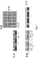
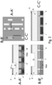
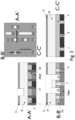
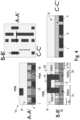
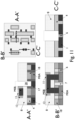
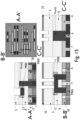
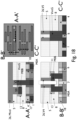
Figs. 1 to 20 are schematic representations of vertical cross-sections through intermediates in the fabrication of an integrated circuit according to an embodiment of the present invention. -
Fig. 21 is a top view of two schematized standard cells according to the prior art. - In the different figures, the same reference signs refer to the same or analogous elements.
- The present invention will be described with respect to particular embodiments and with reference to certain drawings but the invention is not limited thereto but only by the claims. The drawings described are only schematic and are non-limiting. In the drawings, the size of some of the elements may be exaggerated and not drawn on scale for illustrative purposes. The dimensions and the relative dimensions do not correspond to actual reductions to practice of the invention.
- Furthermore, the terms first, second, third and the like in the description and in the claims, are used for distinguishing between similar elements and not necessarily for describing a sequence, either temporally, spatially, in ranking or in any other manner. It is to be understood that the terms so used are interchangeable under appropriate circumstances and that the embodiments of the invention described herein are capable of operation in other sequences than described or illustrated herein.
- Moreover, the terms top, bottom, over, under and the like in the description and the claims are used for descriptive purposes and not necessarily for describing relative positions. It is to be understood that the terms so used are interchangeable under appropriate circumstances and that the embodiments of the invention described herein are capable of operation in other orientations than described or illustrated herein.
- It is to be noticed that the term "comprising", used in the claims, should not be interpreted as being restricted to the means listed thereafter; it does not exclude other elements or steps. It is thus to be interpreted as specifying the presence of the stated features, integers, steps or components as referred to, but does not preclude the presence or addition of one or more other features, integers, steps or components, or groups thereof. The term "comprising" therefore covers the situation where only the stated features are present (and can therefore always be replaced by "consisting of' in order to restrict the scope to said stated features) and the situation where these features and one or more other features are present. The word "comprising" according to the invention therefore also includes as one embodiment that no further components are present. Thus, the scope of the expression "a device comprising means A and B" should not be interpreted as being limited to devices consisting only of components A and B. It means that with respect to the present invention, the only relevant components of the device are A and B.
- Similarly, it is to be noticed that the term "coupled", also used in the claims, should not be interpreted as being restricted to direct connections only. The terms "coupled" and "connected", along with their derivatives, may be used. It should be understood that these terms are not intended as synonyms for each other. Thus, the scope of the expression "a device A coupled to a device B" should not be limited to devices or systems wherein an output of device A is directly connected to an input of device B. It means that there exists a path between an output of A and an input of B which may be a path including other devices or means. "Coupled" may mean that two or more elements are either in direct physical or electrical contact, or that two or more elements are not in direct contact with each other but yet still co-operate or interact with each other.
- Reference throughout this specification to "one embodiment" or "an embodiment" means that a particular feature, structure or characteristic described in connection with the embodiment is included in at least one embodiment of the present invention. Thus, appearances of the phrases "in one embodiment" or "in an embodiment" in various places throughout this specification are not necessarily all referring to the same embodiment, but may. Furthermore, the particular features, structures or characteristics may be combined in any suitable manner, as would be apparent to one of ordinary skill in the art from this disclosure, in one or more embodiments.
- Similarly, it should be appreciated that in the description of exemplary embodiments of the invention, various features of the invention are sometimes grouped together in a single embodiment, figure, or description thereof for the purpose of streamlining the disclosure and aiding in the understanding of one or more of the various inventive aspects. This method of disclosure, however, is not to be interpreted as reflecting an intention that the claimed invention requires more features than are expressly recited in each claim. Rather, as the following claims reflect, inventive aspects lie in less than all features of a single foregoing disclosed embodiment. Thus, the claims following the detailed description are hereby expressly incorporated into this detailed description, with each claim standing on its own as a separate embodiment of this invention.
- Furthermore, while some embodiments described herein include some but not other features included in other embodiments, combinations of features of different embodiments are meant to be within the scope of the invention, and form different embodiments, as would be understood by those in the art. For example, in the following claims, any of the claimed embodiments can be used in any combination.
- Furthermore, some of the embodiments are described herein as a method or combination of elements of a method that can be implemented by a processor of a computer system or by other means of carrying out the function. Thus, a processor with the necessary instructions for carrying out such a method or element of a method forms a means for carrying out the method or element of a method. Furthermore, an element described herein of an apparatus embodiment is an example of a means for carrying out the function performed by the element for the purpose of carrying out the invention.
- In the description provided herein, numerous specific details are set forth. However, it is understood that embodiments of the invention may be practiced without these specific details. In other instances, well-known methods, structures and techniques have not been shown in detail in order not to obscure an understanding of this description.
- The invention will now be described by a detailed description of several embodiments of the invention. It is clear that other embodiments of the invention can be configured according to the knowledge of persons skilled in the art without departing from the technical teaching of the invention, the invention being limited only by the terms of the appended claims.
- We now refer to
Figs. 4 to 20 . - In a first aspect, the present invention relates to a method for forming an integrated circuit or an intermediate (15) in the formation thereof comprising the steps of:
- a. Providing a semiconductor structure (16,
Fig. 4 ) comprising:- i. two transistor structures (3a, 3b) separated by a dielectric separation (7), each transistor structure (3a, 3b) comprising a pMOS side (5p) of a first doping type and an nMOS side (5n) of a second doping type, each side forming a channel structure, a source portion, and a drain portion, the source portion and the drain portion being horizontally separated by said channel structure,
- ii. a gate structure on the channel structure, the gate structure comprising a gate electrode (1) and a gate plug (4),
- iii. electrically conductive contacts (MOA) electrically coupled to the source portion and the drain portion of each side (5p, 5n) of each transistor structure (3a, 3b),
- iv. a first dielectric layer (8) over the two transistor structures (3a, 3b), the gate structure, and the electrically conductive contacts (MOA),
- v. a first electrically conductive line (MOB) embedded in the first dielectric layer (8) so that a top surface (19) of the first electrically conductive line (MOB) and a top surface (20) of the first dielectric layer (8) are coplanar, the first electrically conductive line (MOB) being arranged within a first metallization level and extending along a first direction, the first electrically conductive line (MOB) extending above at least part of each transistor structure (3a, 3b),
- vi. a first electrically conductive via (V0A1) electrically connecting the first electrically conductive line (MOB) with a first electrically conductive contact (M0A1) on a first side (5n, 5p) of a first (3a) of the transistor structures (3a, 3b),
- vii. a second electrically conductive via (V0A2) electrically connecting the first electrically conductive line (MOB) with a second electrically conductive contact (M0A2) on a first side (5n, 5p) of a second (3b) of the transistor structures (3a, 3b),
- b. optionally providing a protection (11,
Figs. 5-7 ) selectively on a top surface of the first electrically conductive line (MOB), - c. recessing the first dielectric layer (8) so as to expose a top portion (2,
Fig. 8 ) of all sidewalls of the first electrically conductive line (MOB), - d. providing spacers (13,
Fig. 9 ) along each sidewall of the first electrically conductive line (MOB), - e. depositing a second dielectric layer (10,
Fig. 10 ) on the first dielectric layer (8) so that a top surface of the spacers (13), a top surface of the protection (11) if present, a top surface of the first electrically conductive line (MOB) if no protection (11) is present, and a top surface of the second dielectric layer (10) are coplanar, - f. etching through the second (10), the first dielectric material (8), and the gate plug (4) by using at least one of the spacers (13) as a mask, thereby forming an opening (28,
Fig. 11 ) exposing a top surface of the gate electrode (1), and - g. providing an electrically conductive material in the opening (28), thereby forming a third electrically conductive via (VintG,
Fig. 12 ). - In
Fig. 4 , the first electrically conductive via (V0A1) is electrically connecting the first electrically conductive line (MOB) with a first electrically conductive contact (M0A1) on a first side, here the p-type side (5p), of a first (3a) of the transistor structures (3a, 3b), while the second electrically conductive via (V0A2) is electrically connecting the first electrically conductive line (MOB) with a second electrically conductive contact (M0A2) on a first side, here an n-type side (5n), of a second (3b) of the transistor structures (3a, 3b). - An alternative starting point for the method of the first aspect is where the first electrically conductive via (V0A1) is electrically connecting the first electrically conductive line (MOB) with a first electrically conductive contact (M0A1) on a first side, here the n-type side (5n), of a first (3a) of the transistor structures (3a, 3b), while the second electrically conductive via (V0A2) is electrically connecting the first electrically conductive line (MOB) with a second electrically conductive contact (M0A2) on a first side, here also an n-type side (5n), of a second (3b) of the transistor structures (3a, 3b).
- Yet another alternative starting point for the method of the first aspect is where the first electrically conductive via (V0A1) is electrically connecting the first electrically conductive line (MOB) with a first electrically conductive contact (M0A1) on a first side, here the n-type side (5n), of a first (3a) of the transistor structures (3a, 3b), while the second electrically conductive via (V0A2) is electrically connecting the first electrically conductive line (MOB) with a second electrically conductive contact (M0A2) on a first side, here a p-type side (5p), of a second (3b) of the transistor structures (3a, 3b).
- Yet another alternative starting point for the method of the first aspect is where the first electrically conductive via (V0A1) is electrically connecting the first electrically conductive line (MOB) with a first electrically conductive contact (M0A1) on a first side, here the p-type side (5p), of a first (3a) of the transistor structures (3a, 3b), while the second electrically conductive via (V0A2) is electrically connecting the first electrically conductive line (MOB) with a second electrically conductive contact (M0A2) on a first side, here a p-type side (5p), of a second (3b) of the transistor structures (3a, 3b).
- All these alternatives are valid starting points for performed thereon steps b and following. We now refer to
Figs. 1 to 4 . In embodiments, step a may comprise the steps of: - a1. Providing a semiconductor structure (see
Fig. 1 ) comprising- (i) two transistor structures (3a, 3b) separated by a dielectric separation (7), each transistor structure (3a, 3b) comprising a pMOS side (5p) of a first doping type and an nMOS side (5n) of a second doping type, each side forming a channel structure, a source portion, and a drain portion, the source portion and the drain portion being horizontally separated by said channel structure,
- (ii) a gate structure on the channel structure, the gate structure comprising a gate electrode (1) and a gate plug (4), and
- (iii) electrically conductive contacts (MOA) electrically coupled to the source portion and the drain portion of each side (5p, 5n) of each transistor structure (3a, 3b),
- a2. Providing a first dielectric layer (8,
Fig. 2 ) over the two transistor structures (3a, 3b), the gate structure, and the electrically conductive contacts (MOA), - a3. Providing a first hard mask (9,
Fig. 2 ) over the first dielectric layer (8), the first hard mask (9) having an opening (22) having its length extending along a first direction, the opening (22) extending above at least part of each transistor structure (3a, 3b), - a4. Etching partly through the first dielectric layer (8) by using the first hard mask (9) as a mask, thereby forming a trench (21,
Fig. 2 ) which bottom is formed by the first dielectric layer (8), - a5. Covering a central portion of the bottom with a second hard mask (not depicted), and etching two holes (23,
Fig. 3 ), one on each side of the second hard mask, by using the first and second hard masks as masks, thereby exposing a first electrically conductive contact (M0A1) and a second electrically conductive contact (M0A2), - a6. Removing the first hard mask (9,
Fig. 4 ) and second hard mask, and - a7. Filling both holes (23) and the trench (21) with an electrically conductive material, thereby forming a first electrically conductive line (M0B,
Fig. 4 ), the first electrically conductive via (V0A1), and the second electrically conductive via (V0A2). - In embodiments, the two transistor structures (3a, 3b) may be two nanosheet transistor structures (3a, 3b), each nanosheet transistor structure comprising two nanosheet stacks, one stack forming the pMOS side (5p) of a first doping type, and another stack forming the nMOS side (5n) of a second doping type, each side (5p, 5n) comprising a plurality of vertically stacked nanosheets, said plurality forming a channel structure, a source portion, and a drain portion, the source portion and the drain portion being horizontally separated by said channel structure.
- In preferred embodiments, the two transistor structures (3a, 3b) may be two transistor structures (3a, 3b), wherein the pMOS side (5p) of a first doping type and the nMOS side (5n) of a second doping type are separated by a dielectric wall (6), each side (5p, 5n) comprising a plurality of vertically stacked nanosheets, said plurality forming a channel structure, a source portion, and a drain portion, the source portion and the drain portion being horizontally separated by said channel structure, each nanosheet having one side touching said dielectric wall. Such transistor structures are called forksheet transistor structures. This is advantageous because it gives more space for the active devices than if nanosheets are used. Indeed, the p-n separation takes significantly less place if forksheet transistor structures (3a, 3b) are used. The reason for this is the presence of the dielectric wall (6) between the nMOS and the pMOS.
- In embodiments, the dielectric separation (7) may be made of SiO2.
- In embodiments, the gate may comprise a gate metal (1) such as W. Above the gate metal (1), a gate plug (4) is typically present. For this gate plug (4), for instance, Si3N4 can be used. Gate spacers (17) on both sides of the gate are typically present. These gate spacers (17) can for instance be made of Si3N4 or silicon oxycarbide. An example of a gate structure is visible in
Fig. 4 (1, 4, 17). - The source and the drain electrically conductive contacts (M0A1, M0A2) can for instance be SiGe:B (p-MOS) or Si:P (n-MOS).
- Also depicted in
Fig. 1 , is the typical presence of a first active plug (18) above and in physical contact with the first electrically conductive contact (M0A1) and of a second active plug (18) above and in physical contact with the second electrically conductive contact (M0A2). The top surface of the active plug (18) is coplanar with the top surface of the gate spacers (17) and of the gate plug (4). The active plugs (18) are typically formed of a dielectric material such as SiO2. This SiO2 can, for instance, be deposited by plasma enhanced atomic layer deposition. - In embodiments, the first electrically conductive line (MOB) may be embedded in a dielectric material (8).
- In embodiments, the first electrically conductive line (MOB) is provided as part of a set of parallel first electrically conductive lines (MOB), all arranged within a first metallization level and each extending along a same first direction.
- In embodiments, the set of first electrically conductive lines (MOB) may be arranged at a pitch of from 20 to 60 nm, preferably, from 30 to 50 nm, more preferably from 35 to 45 nm, yet more preferably from 37 to 41 nm, and most preferably from 38 to 40 nm. This pitch being relatively large, there is enough space between the set of first electrically conductive lines (MOB) to eventually form the via (VintG) electrically connected with a gate (1).
- The planar dielectric material (8) may for instance be SiO2.
- In embodiments, each of the first electrically conductive line (MOB) and the first and second electrically conductive vias (V0A1, V0A2) may be made of a metal independently selected from metals such as Cu, Mo, Ru, or W, amongst others.
- We now refer to
Figs. 5 to 7 which depict two alternative embodiments to perform step b. - In all embodiments where step b is present, the protection (11) may be a dielectric protection. In some embodiments where step b is present and where the first electrically conductive line (MOB) is made of W or Mo, the protection (11) may be selected from dielectric materials, Cu, and Ru. Cu and Ru tend to be more resistant to the recessing conditions used in step c. In particular, it is significantly more resistant than W or Mo to fluorine-based plasma.
- In embodiments, as for instance illustrated in
Fig. 5 , step b is present, and the protection (11) may be selected from TiOx (e.g., TiO2), silicon oxycarbide, silicon nitride, or even Cu or Ru if the first electrically conductive line (MOB) is made of W or Mo. - In embodiments, as for instance illustrated in
Figs. 6 and7 , step b is present and comprises step b1 (Fig. 6 ) of partially recessing the first electrically conductive line (MOB), and the step b2 (Fig. 7 ) of providing the protection (11) in the recess (24) in such a way that a top surface of the protection (11) is coplanar with a top surface of the first dielectric layer (8). - In alternative embodiments, step b is present, and comprises step b1 of partially recessing the first electrically conductive line (MOB), and the step b2 of providing the protection (11) in the recess (24) in such a way that a top surface of the protection (11) is coplanar with a top surface of the first dielectric layer (8).
- Step b is not necessarily present because the material forming the first electrically conductive line (MOB) is different from the material forming the first dielectric layer (8), thereby allowing finding some recessing conditions with some selectivity toward the dielectric layer (8) with respect to the first electrically conductive line (M0B). If the first electrically conductive line (MOB) is W or Mo and the dielectric layer (8) is a silicon oxide, selectivity might in some case be insufficient, at least if a fluorine-based plasma is used for step c. In such a case, the protection (11) is preferably used. If the first electrically conductive line (MOB) is Cu or Ru and the dielectric layer (8) is a silicon oxide, selectivity with typically be sufficient if a fluorine-based plasma is used. However, also in this case, the protection (11) could be used. Step c can for instance be performed with a fluorine-containing plasma, e.g., a SF6, CF4, CHF3, or C4F containing plasma.
- In embodiments, the spacers (13) may be made of silicon nitride, silicon carbon nitride, silicon carbon oxynitride, or silicon oxycarbide.
- In embodiments, the spacers (13) may have a thickness of from 3 to 9 nm, preferably 4 to 8 nm, more preferably 5 to 7 nm.
- We now refer to
Figs. 13 to 20 . In embodiments, the method may further comprise the following steps: - h. Providing a third dielectric layer (5,
Fig. 13 ) on the second dielectric layer (10), the top surface of the spacers (13), a top surface of the third electrically conductive via (VintG), and either the top surface of the first electrically conductive line (MOB) if step b was not performed or the top surface of the protection (11) otherwise, - i. Providing a hard mask (25,
Fig. 14 ) on a top surface of the third dielectric layer (5), the hard mask (25) having two openings (29), a separation (S1) between both openings (29) being smaller than a space (S2) between the first electrically conductive via (V0A1) and the second electrically conductive via (V0A2), the separation (S1) being directly above the space (S2) between the first electrically conductive via (V0A1) and the second electrically conductive via (V0A2), one of said openings (29) laterally overlapping with the third electrically conductive via (VintG), - j. Etching through the third dielectric layer (5) and through the protection (11) if present by using the hard mask (25) as a mask, thereby forming two longitudinal openings (29, see
Figs. 14-16 ) extending along a second direction, typically perpendicular to the first direction, each of said longitudinal openings (29) exposing the first electrically conductive line (MOB) and the third electrically conductive via (VintG) by means of respectively a first and a second via hole communicating with the longitudinal openings (29), - k. Providing an electrically conductive material (26,
Fig. 17 ) in the two longitudinal openings (29), thereby forming:- two second electrically conductive lines (Mintl1, Mintl2) arranged within a second metallization level, and extending along the second direction, separated by the separation S1, and
- two fourth electrically conductive vias (V4), one of them being directly physically connected to one of the two second electrically conductive lines (Mintl) and to the first electrically conductive line (MOB), the other one being directly physically connected to the other of the two second electrically conductive lines (Mintl) and to the first electrically conductive line (MOB), and
- two fifth electrically conductive vias (V5), one of them being directly physically connected to one of the two second electrically conductive lines (Mintl) and to the third electrically conductive via (VintG), the other one being directly physically connected to the other of the two second electrically conductive lines (Mintl) and to the third electrically conductive via (VintG),
- 1. Etching (see
Fig. 18 ) between both fourth electrically conductive vias (V4), through the entire thickness of the first electrically conductive line (MOB), by using both fourth electrically conductive vias as masks, thereby cutting the first electrically conductive line (MOB), thereby forming a first interruption (30) within the first electrically conductive line (MOB), and - m. Etching (see
Fig. 19 ) between both fifth electrically conductive vias (V5), through the entire thickness of the third electrically conductive via (VintG), by using both electrically conductive vias as masks, thereby cutting the third electrically conductive via (VintG), thereby forming a second interruption (31) within the third electrically conductive via (VintG). - In embodiments, step j may comprise:
- (i) etching through the third dielectric layer (5) by using the hard mask (25) as a mask, thereby forming two longitudinal openings (29, see
Figs. 14 ) extending along a second direction, typically perpendicular to the first direction, - (ii) masking with a mask (e.g., a trilayer SOG/SOC/photoresist) sections of the two longitudinal openings that do not overlap with the first electrically conductive line (MOB),
- (iii) etching through the third dielectric layer (5), and through the protection (11) if present, by using the mask provided in step (ii) and the hard mask (25) as mask, thereby exposing the first electrically conductive line (MOB) by means of a first via hole communicating with the longitudinal openings (29),
- (iv) masking with a mask (e.g., a trilayer SOG/SOC/photoresist) sections of the two longitudinal openings that do not overlap with the the third electrically conductive via (VintG),
- (v) etching through the third dielectric layer (5) by using the mask provided in step (iv) and the hard mask (25) as a mask, thereby exposing the third electrically conductive via (VintG) by means of second via hole communicating with the longitudinal openings (29),
- In embodiments, the method may further comprise, after step m, the step n of filling the first (30) and the second interruption (31) with a dielectric material (27,
Fig. 20 ). - In embodiments, the method may further comprise the step o, after step m or step n, of forming:
- (i) above the second metallization level, a set of third electrically conductive lines (M1l) arranged within a third metallization level, and extending along the first direction, and
- (ii) a via (V1) electrically connecting a third electrically conductive line (M1l) with a second electrically conductive line (Mintl).
- In embodiments, the method of the first aspect may be for forming a standard cell of the integrated circuit.
- In embodiments, the standard cell may comprise four second electrically conductive lines (Mintl) and more than four third electrically conductive lines (M1l).
- Steps 1 and m of etching respectively between both fourth electrically conductive vias (V4) and both fifth electrically conductive vias (V5) may be performed by any suitable method. For instance, if both fourth electrically conductive vias (V4) and both fifth electrically conductive vias (V5) are made of Ru, etching can be performed by plasma etching using Cl2 and/or O2 and Cl2 as etchant gas in an inductively coupled plasma etching chamber.
- In embodiments, the set of second electrically conductive lines (Mintl) may be arranged at a pitch of from 9 to 30 nm, preferably, from 11 to 25 nm, more preferably from 14 to 22 nm, yet more preferably from 16 to 20 nm, and most preferably from 18 to 20 nm.
- In embodiments, the set of second electrically conductive lines (Mintl) may be arranged at a pitch and the width of the first interruption (30) as well as the width of the second interruption (31) are equal to 0.5 times the pitch.
- In embodiments, the distance separating both fourth electrically conductive vias (V4) may be 0.5 times the pitch of the set of second electrically conductive lines (Mintl).
- In embodiments, the width of each of the fourth electrically conductive vias (V4) measured along the first direction is preferably from 5 to 13 nm, more preferably from 6 to 11 nm, yet more preferably from 7 to 11 nm, and most preferably from 8 to 10 nm. Typically, the width for these two vias is 9 nm.
- In embodiments, the distance separating both fourth electrically conductive vias (V4) may be preferably from 5 to 13 nm, more preferably from 6 to 11 nm, yet more preferably from 7 to 11 nm, and most preferably from 8 to 10 nm. Typically, these two vias are separated by 9 nm.
- In embodiments, the first (30) and the second interruption (31) may each have a width of from 5 to 13 nm, more preferably from 6 to 11 nm, yet more preferably from 7 to 11 nm, and most preferably from 8 to 10 nm. Typically, these interruptions have a width of 9 nm. Such a small interruption, let alone with perfect alignment to the gap, has up to now been very challenging. It is, however, easily achieved with the method of the present invention.
- In a second aspect, the present invention relates to an integrated circuit or an intermediate (15) in the fabrication thereof obtainable by any embodiment of the first aspect.
- In embodiments of the second aspect, the present invention relates to an integrated circuit or an intermediate (15) in the fabrication of an integrated circuit comprising:
- a. a semiconductor structure (16) comprising:
- i. two transistor structures (3a, 3b) separated by a dielectric separation (7), each transistor structure (3a, 3b) comprising a pMOS side (5p) of a first doping type and an nMOS side (5n) of a second doping type, each side forming a channel structure, a source portion, and a drain portion, the source portion and the drain portion being horizontally separated by said channel structure,
- ii. a gate structure on the channel structure, the gate structure comprising a gate electrode (1),
- iii. electrically conductive contacts (MOA) electrically coupled to the source portion and the drain portion of each side (5p, 5n) of each transistor structure (3a, 3b),
- iv. a first dielectric layer (8) over the two transistor structures (3a, 3b), the gate structure, and the electrically conductive contacts (MOA),
- v. a first electrically conductive line (MOB) embedded in the first dielectric layer (8), the first electrically conductive line (MOB) being arranged within a first metallization level and extending along a first direction,
- vi. a first electrically conductive via (V0A1) electrically connecting the first electrically conductive line (MOB) with a first electrically conductive contact (M0A1) on a first side (5n, 5p) of a first (3a) of the transistor structures (3a, 3b),
- vii. a second electrically conductive via (V0A2) electrically connecting the first electrically conductive line (MOB) with a second electrically conductive contact (M0A2) on a first side (5n, 5p) of a second (3b) of the transistor structures (3a, 3b),
- viii. spacers (13) along sidewalls of the first electrically conductive line (MOB),
- ix. a third electrically conductive via (VintG) through the second (10) and first dielectric material (8) and touching a spacer (13) and the gate electrode (1).
- In embodiments, the first electrically conductive line (MOB) extends above at least part of each transistor structure (3a, 3b) and the spacers (13) are along each sidewall of the first electrically conductive line (M0B). This is the case at least in
Figs. 12 to 17 . In other embodiments corresponding for instance toFigs. 18 to 20 , the first electrically conductive line (MOB) comprises two parts separated by a first interruption (30) within the first electrically conductive line (MOB), a first part extending above at least part of a first transistor structure (3a) and a second part extending above at least part of a second transistor structure (3b), thereby electrically separating the first electrically conductive via (V0A1) from the second electrically conductive via (V0A2), and the spacers are along each sidewall of each part of the first electrically conductive line (MOB) except along the sidewalls facing the interruption (30). - In other embodiments, the first electrically conductive line (MOB) may comprise a gap cutting the first electrically conductive line (MOB) in two, thereby electrically separating the first electrically conductive via (V0A1) from the second electrically conductive via (V0A2).
- Any feature of the second aspect may be as correspondingly described in any embodiments of the second first aspect.
- It is to be understood that although preferred embodiments, specific constructions and configurations, as well as materials, have been discussed herein for devices according to the present invention, various changes or modifications in form and detail may be made without departing from the scope of this invention. For example, any formulas given above are merely representative of procedures that may be used. Functionality may be added or deleted from the block diagrams and operations may be interchanged among functional blocks. Steps may be added or deleted to methods described within the scope of the present invention.
Claims (15)
- A method for forming an integrated circuit or an intermediate (15) in the formation thereof comprising the steps of:a. Providing a semiconductor structure (16) comprising:i. two transistor structures (3a, 3b) separated by a dielectric separation (7), each transistor structure (3a, 3b) comprising a pMOS side (5p) of a first doping type and an nMOS side (5n) of a second doping type, each side forming a channel structure, a source portion, and a drain portion, the source portion and the drain portion being horizontally separated by said channel structure,ii. a gate structure on the channel structure, the gate structure comprising a gate electrode (1) and a gate plug (4),iii. electrically conductive contacts (MOA) electrically coupled to the source portion and the drain portion of each side (5p, 5n) of each transistor structure (3a, 3b),iv. a first dielectric layer (8) over the two transistor structures (3a, 3b), the gate structure, and the electrically conductive contacts (MOA),v. a first electrically conductive line (MOB) embedded in the first dielectric layer (8) so that a top surface (19) of the first electrically conductive line (MOB) and a top surface (20) of the first dielectric layer (8) are coplanar, the first electrically conductive line (MOB) being arranged within a first metallization level and extending along a first direction, the first electrically conductive line (MOB) extending above at least part of each transistor structure (3a, 3b),vi. a first electrically conductive via (V0A1) electrically connecting the first electrically conductive line (MOB) with a first electrically conductive contact (M0A1) on a first side (5n, 5p) of a first (3a) of the transistor structures (3a, 3b),vii. a second electrically conductive via (V0A2) electrically connecting the first electrically conductive line (MOB) with a second electrically conductive contact (M0A2) on a first side (5n, 5p) of a second (3b) of the transistor structures (3a, 3b),b. optionally providing a protection (11) selectively on a top surface of the first electrically conductive line (MOB),c. recessing the first dielectric layer (8) so as to expose a top portion (2) of all sidewalls of the first electrically conductive line (MOB),d. providing spacers (13) along each sidewall of the first electrically conductive line (MOB),e. depositing a second dielectric layer (10) on the first dielectric layer (8) so that a top surface of the spacers (13), a top surface of the protection (11) if present, a top surface of the first electrically conductive line (MOB) if no protection (11) is present, and a top surface of the second dielectric layer (10) are coplanar,f. etching through the second (10), the first dielectric material (8), and the gate plug (4) by using at least one of the spacers (13) as a mask, thereby forming an opening (28) exposing a top surface of the gate electrode (1), andg. providing an electrically conductive material (14) in the opening (28), thereby forming a third electrically conductive via (VintG).
- The method according to claim 1, wherein the two transistor structures (3a, 3b) are two transistor structures (3a, 3b), wherein the pMOS side (5p) of a first doping type and the nMOS side (5n) of a second doping type are separated by a dielectric wall (6), each side (5p, 5n) comprising a plurality of vertically stacked nanosheets, said plurality forming a channel structure, a source portion, and a drain portion, the source portion and the drain portion being horizontally separated by said channel structure, each nanosheet having one side touching said dielectric wall (6).
- The method according to any one of the preceding claims, wherein step a comprises the steps of:a1. Providing a semiconductor structure comprising(i) two transistor structures (3a, 3b) separated by a dielectric separation (7), each transistor structure (3a, 3b) comprising a pMOS side (5p) of a first doping type and an nMOS side (5n) of a second doping type, each side forming a channel structure, a source portion, and a drain portion, the source portion and the drain portion being horizontally separated by said channel structure,(ii) a gate structure on the channel structure, the gate structure comprising a gate electrode (1) and a gate plug (4), and(iii) electrically conductive contacts (MOA) electrically coupled to the source portion and the drain portion of each side (5p, 5n) of each transistor structure (3a, 3b),a2. Providing a first dielectric layer (8) over the two transistor structures (3a, 3b), the gate structure, and the electrically conductive contacts (MOA),a3. Providing a first hard mask (9) over the first dielectric layer (8), the first hard mask (9) having an opening (22) having its length extending along a first direction, the opening (22) extending above at least part of each transistor structure (3a, 3b),a4. Etching partly through the first dielectric layer (8) by using the first hard mask (9) as a mask, thereby forming a trench (21) which bottom is formed by the first dielectric layer (8),a5. Covering a central portion of the bottom with a second hard mask, and etching two holes (23), one on each side of the second hard mask, by using the first and second hard masks as masks, thereby exposing a first electrically conductive contact (M0A1) and a second electrically conductive contact (M0A2),a6. Removing the first hard mask (9) and second hard mask, anda7. Filling both holes (23) and the trench (21) with an electrically conductive material, thereby forming a first electrically conductive line (MOB), the first electrically conductive via (V0A1), and the second electrically conductive via (V0A2).
- The method according to any one of the preceding claims, wherein step b is present and the protection (11) is a dielectric protection (11).
- The method according to claim 4, wherein step b is present and the dielectric protection (11) is TiO2.
- The method according to any one of claims 1 to 5, wherein step b is present and comprises step b1 of partially recessing the first electrically conductive line (MOB), and the step b2 of providing the protection (11) in the recess (24) in such a way that a top surface of the protection (11) is coplanar with a top surface of the first dielectric layer (8).
- The method according to any one of the preceding claims, wherein the spacers (13) are made of silicon nitride, silicon carbon nitride, silicon carbon oxynitride, or silicon oxycarbide.
- The method according to any one of the preceding claims, wherein the spacers (13) have a thickness of from 3 to 9 nm, preferably 4 to 8 nm, more preferably 5 to 7 nm.
- The method according to any one of the preceding claims, further comprising the following steps:h. Providing a third dielectric layer (5) on the second dielectric layer (10), the top surface of the spacers (13), a top surface of the third electrically conductive via (VintG), and either the top surface of the first electrically conductive line (MOB) if step b was not performed or the top surface of the protection (11) otherwise,i. Providing a hard mask (25) on a top surface of the third dielectric layer (5), the hard mask (25)having two openings (29), a separation (s1) between both openings (29) being smaller than a space (s2) between the first electrically conductive via (V0A1) and the second electrically conductive via (V0A2), the separation (s1) being directly above a space (s2) between the first electrically conductive via (V0A1) and the second electrically conductive via (V0A2), one of said openings (29) laterally overlapping with the third electrically conductive via (VintG),j. Etching through the third dielectric layer (5) and through the protection (11) if present by using the hard mask (25) as a mask, thereby forming two longitudinal openings (29), extending along a second direction, typically perpendicular to the first direction, each of said longitudinal openings (29) exposing the first electrically conductive line (MOB) and the third electrically conductive via (VintG) by means of respectively a first and a second via hole communicating with the longitudinal openings (29),k. Providing an electrically conductive material (26) in the two longitudinal openings (29), thereby forming thereby forming:- two second electrically conductive lines (Mintl1, Mintl2) arranged within a second metallization level, and extending along the second direction, separated by the separation S1, and- two fourth electrically conductive vias (V4), one of them being directly physically connected to one of the two second electrically conductive lines (Mintl) and to the first electrically conductive line (MOB), the other one being directly physically connected to the other of the two second electrically conductive lines (Mintl) and to the first electrically conductive line (MOB), and- two fifth electrically conductive vias (V5), one of them being directly physically connected to one of the two second electrically conductive lines (Mintl) and to the third electrically conductive via (VintG), the other one being directly physically connected to the other of the two second electrically conductive lines (Mintl) and to the third electrically conductive via (VintG),1. Etching between both fourth electrically conductive vias (V4), through the entire thickness of the first electrically conductive line (MOB), by using both fourth electrically conductive vias as masks, thereby cutting the first electrically conductive line (MOB), thereby forming a first interruption (30) within the first electrically conductive line (MOB), andm. Etching between both fifth electrically conductive vias (V5), through the entire thickness of the third electrically conductive via (VintG), by using both electrically conductive vias as masks, thereby cutting the third electrically conductive via (VintG), thereby forming a second interruption (31) within the third electrically conductive via (VintG).
- The method according to claim 9, further comprising, after step m, the step n of filling the first (30) and the second interruption (31) with a dielectric material (27).
- The method according to claim 9 or claim 10, further comprising, after step m or step n, the step o of forming:(i) above the second metallization level, a set of third electrically conductive lines (M1l) arranged within a third metallization level, and extending along the first direction, and(ii) a via (V1) electrically connecting a third electrically conductive line (M1l) with a second electrically conductive line (Mintl).
- The method according to any one of claims 1 to 11 for forming a standard cell of the integrated circuit.
- The method according to claim 12 as depending on claim 11, wherein the standard cell comprises four second electrically conductive lines (Mintl) and more than four third electrically conductive lines (M1l).
- An integrated circuit or an intermediate (15) in the fabrication of an integrated circuit comprising:a. A semiconductor structure (16) comprising:i. two transistor structures (3a, 3b) separated by a dielectric separation (7), each transistor structure (3a, 3b) comprising a pMOS side (5p) of a first doping type and an nMOS side (5n) of a second doping type, each side forming a channel structure, a source portion, and a drain portion, the source portion and the drain portion being horizontally separated by said channel structure,ii. a gate structure on the channel structure, the gate structure comprising a gate electrode (1),iii. electrically conductive contacts (MOA) electrically coupled to the source portion and the drain portion of each side (5p, 5n) of each transistor structure (3a, 3b),iv. a first dielectric layer (8) over the two transistor structures (3a, 3b), the gate structure, and the electrically conductive contacts (MOA),v. a first electrically conductive line (MOB) embedded in the first dielectric layer (8), the first electrically conductive line (MOB) being arranged within a first metallization level and extending along a first direction,vi. a first electrically conductive via (V0A1) electrically connecting the first electrically conductive line (MOB) with a first electrically conductive contact (M0A1) on a first side (5n, 5p) of a first (3a) of the transistor structures (3a, 3b),vii. a second electrically conductive via (V0A2) electrically connecting the first electrically conductive line (MOB) with a second electrically conductive contact (M0A2) on a first side (5n, 5p) of a second (3b) of the transistor structures (3a, 3b),viii. spacers (13) along sidewalls of the first electrically conductive line (MOB),ix. a third electrically conductive via (VintG) through the second (10) and first dielectric material (8) and touching a spacer (13) and the gate electrode (1).
- An integrated circuit or an intermediate (15) in the fabrication of an integrated circuit according to claim 14, wherein either:a. the first electrically conductive line (MOB) extends above at least part of each transistor structure (3a, 3b) and the spacers (13) are along each sidewall of the first electrically conductive line (MOB), orb. the first electrically conductive line (MOB) comprises two parts separated by a first interruption (30) within the first electrically conductive line (MOB), a first part extending above at least part of a first transistor structure (3a) and a second part extending above at least part of a second transistor structure (3b), thereby electrically separating the first electrically conductive via (V0A1) from the second electrically conductive via (V0A2), and the spacers are along each sidewall of each part of the first electrically conductive line (MOB) except along the sidewalls facing the interruption (30).
Priority Applications (3)
| Application Number | Priority Date | Filing Date | Title |
|---|---|---|---|
| EP21216251.5A EP4202986B1 (en) | 2021-12-21 | 2021-12-21 | Via formation in an integrated circuit |
| US18/054,228 US12519015B2 (en) | 2021-12-21 | 2022-11-10 | Conductive via formation connecting transistor structures in an integrated circuit |
| CN202211550672.0A CN116314009A (en) | 2021-12-21 | 2022-12-05 | Via formation in integrated circuits |
Applications Claiming Priority (1)
| Application Number | Priority Date | Filing Date | Title |
|---|---|---|---|
| EP21216251.5A EP4202986B1 (en) | 2021-12-21 | 2021-12-21 | Via formation in an integrated circuit |
Publications (2)
| Publication Number | Publication Date |
|---|---|
| EP4202986A1 true EP4202986A1 (en) | 2023-06-28 |
| EP4202986B1 EP4202986B1 (en) | 2024-05-01 |
Family
ID=78957700
Family Applications (1)
| Application Number | Title | Priority Date | Filing Date |
|---|---|---|---|
| EP21216251.5A Active EP4202986B1 (en) | 2021-12-21 | 2021-12-21 | Via formation in an integrated circuit |
Country Status (3)
| Country | Link |
|---|---|
| US (1) | US12519015B2 (en) |
| EP (1) | EP4202986B1 (en) |
| CN (1) | CN116314009A (en) |
Families Citing this family (1)
| Publication number | Priority date | Publication date | Assignee | Title |
|---|---|---|---|---|
| EP4199052B1 (en) * | 2021-12-17 | 2024-08-21 | IMEC vzw | Metallization scheme for an integrated circuit |
Citations (3)
| Publication number | Priority date | Publication date | Assignee | Title |
|---|---|---|---|---|
| US20130248990A1 (en) * | 2012-03-21 | 2013-09-26 | Samsung Electronics Co., Ltd. | Semiconductor devices and method for fabricating the same |
| US20160005822A1 (en) * | 2014-07-01 | 2016-01-07 | Qualcomm Incorporated | Self-aligned via for gate contact of semiconductor devices |
| US20190181042A1 (en) * | 2017-12-11 | 2019-06-13 | Globalfoundries Inc. | Methods of forming contact structures on integrated circuit products |
-
2021
- 2021-12-21 EP EP21216251.5A patent/EP4202986B1/en active Active
-
2022
- 2022-11-10 US US18/054,228 patent/US12519015B2/en active Active
- 2022-12-05 CN CN202211550672.0A patent/CN116314009A/en active Pending
Patent Citations (3)
| Publication number | Priority date | Publication date | Assignee | Title |
|---|---|---|---|---|
| US20130248990A1 (en) * | 2012-03-21 | 2013-09-26 | Samsung Electronics Co., Ltd. | Semiconductor devices and method for fabricating the same |
| US20160005822A1 (en) * | 2014-07-01 | 2016-01-07 | Qualcomm Incorporated | Self-aligned via for gate contact of semiconductor devices |
| US20190181042A1 (en) * | 2017-12-11 | 2019-06-13 | Globalfoundries Inc. | Methods of forming contact structures on integrated circuit products |
Also Published As
| Publication number | Publication date |
|---|---|
| EP4202986B1 (en) | 2024-05-01 |
| US12519015B2 (en) | 2026-01-06 |
| US20230197528A1 (en) | 2023-06-22 |
| CN116314009A (en) | 2023-06-23 |
Similar Documents
| Publication | Publication Date | Title |
|---|---|---|
| US12243913B2 (en) | Self-aligned backside contact integration for transistors | |
| US20230187561A1 (en) | Semiconductor Structure Having Both Gate-All-Around Devices and Planar Devices | |
| US20230197514A1 (en) | Metallization Process for an Integrated Circuit | |
| US10847415B2 (en) | Self-aligned gate contact | |
| US20190386011A1 (en) | Semiconductor device and method of forming semiconductor device | |
| EP3740970B1 (en) | A novel standard cell architecture for gate tie-off | |
| US20050073005A1 (en) | High-density split-gate finfet | |
| US20060019488A1 (en) | Method of forming a static random access memory with a buried local interconnect | |
| US7518190B2 (en) | Grounding front-end-of-line structures on a SOI substrate | |
| US20050023617A1 (en) | Conductive lines buried in insulating areas | |
| JP2004193588A (en) | Vertical MOSFET (vertical MOSFET) SRAM cell | |
| US20070080380A1 (en) | Self-aligned gate isolation | |
| TW201839860A (en) | Air gap near the bottom source/turn region of the vertical transistor device | |
| US20240006313A1 (en) | Self-aligned backside connections for transistors | |
| EP4202986B1 (en) | Via formation in an integrated circuit | |
| CN112216695A (en) | Semiconductor device and method of forming the same | |
| CN218004863U (en) | Semiconductor device with a plurality of semiconductor chips | |
| JP2025502153A (en) | Interconnects in diffusion breaks in integrated circuits | |
| US7445973B2 (en) | Transistor surround gate structure with silicon-on-insulator isolation for memory cells, memory arrays, memory devices and systems and methods of forming same | |
| KR20090125247A (en) | Trench Formation in Semiconductor Materials | |
| CN212517203U (en) | Basic digital logic unit, integrated circuit layout and semiconductor device | |
| US20240213312A1 (en) | Integrated Circuit Devices and Methods for Making Such Devices | |
| US20060231891A1 (en) | SOI SRAM products with reduced floating body effect and the method thereof | |
| KR20210148820A (en) | Three-dimensional memory device and methods of forming | |
| US20260026088A1 (en) | Area scaling using an extended full cut with a supporting backside gate jumper |
Legal Events
| Date | Code | Title | Description |
|---|---|---|---|
| PUAI | Public reference made under article 153(3) epc to a published international application that has entered the european phase |
Free format text: ORIGINAL CODE: 0009012 |
|
| STAA | Information on the status of an ep patent application or granted ep patent |
Free format text: STATUS: THE APPLICATION HAS BEEN PUBLISHED |
|
| AK | Designated contracting states |
Kind code of ref document: A1 Designated state(s): AL AT BE BG CH CY CZ DE DK EE ES FI FR GB GR HR HU IE IS IT LI LT LU LV MC MK MT NL NO PL PT RO RS SE SI SK SM TR |
|
| STAA | Information on the status of an ep patent application or granted ep patent |
Free format text: STATUS: REQUEST FOR EXAMINATION WAS MADE |
|
| 17P | Request for examination filed |
Effective date: 20231023 |
|
| RBV | Designated contracting states (corrected) |
Designated state(s): AL AT BE BG CH CY CZ DE DK EE ES FI FR GB GR HR HU IE IS IT LI LT LU LV MC MK MT NL NO PL PT RO RS SE SI SK SM TR |
|
| GRAP | Despatch of communication of intention to grant a patent |
Free format text: ORIGINAL CODE: EPIDOSNIGR1 |
|
| STAA | Information on the status of an ep patent application or granted ep patent |
Free format text: STATUS: GRANT OF PATENT IS INTENDED |
|
| INTG | Intention to grant announced |
Effective date: 20240123 |
|
| RAP3 | Party data changed (applicant data changed or rights of an application transferred) |
Owner name: IMEC VZW |
|
| P01 | Opt-out of the competence of the unified patent court (upc) registered |
Effective date: 20240208 |
|
| GRAS | Grant fee paid |
Free format text: ORIGINAL CODE: EPIDOSNIGR3 |
|
| GRAA | (expected) grant |
Free format text: ORIGINAL CODE: 0009210 |
|
| STAA | Information on the status of an ep patent application or granted ep patent |
Free format text: STATUS: THE PATENT HAS BEEN GRANTED |
|
| AK | Designated contracting states |
Kind code of ref document: B1 Designated state(s): AL AT BE BG CH CY CZ DE DK EE ES FI FR GB GR HR HU IE IS IT LI LT LU LV MC MK MT NL NO PL PT RO RS SE SI SK SM TR |
|
| REG | Reference to a national code |
Ref country code: GB Ref legal event code: FG4D |
|
| REG | Reference to a national code |
Ref country code: CH Ref legal event code: EP |
|
| REG | Reference to a national code |
Ref country code: IE Ref legal event code: FG4D |
|
| REG | Reference to a national code |
Ref country code: DE Ref legal event code: R096 Ref document number: 602021012640 Country of ref document: DE |
|
| REG | Reference to a national code |
Ref country code: LT Ref legal event code: MG9D |
|
| REG | Reference to a national code |
Ref country code: NL Ref legal event code: MP Effective date: 20240501 |
|
| PG25 | Lapsed in a contracting state [announced via postgrant information from national office to epo] |
Ref country code: IS Free format text: LAPSE BECAUSE OF FAILURE TO SUBMIT A TRANSLATION OF THE DESCRIPTION OR TO PAY THE FEE WITHIN THE PRESCRIBED TIME-LIMIT Effective date: 20240901 |
|
| PG25 | Lapsed in a contracting state [announced via postgrant information from national office to epo] |
Ref country code: BG Free format text: LAPSE BECAUSE OF FAILURE TO SUBMIT A TRANSLATION OF THE DESCRIPTION OR TO PAY THE FEE WITHIN THE PRESCRIBED TIME-LIMIT Effective date: 20240501 |
|
| PG25 | Lapsed in a contracting state [announced via postgrant information from national office to epo] |
Ref country code: FI Free format text: LAPSE BECAUSE OF FAILURE TO SUBMIT A TRANSLATION OF THE DESCRIPTION OR TO PAY THE FEE WITHIN THE PRESCRIBED TIME-LIMIT Effective date: 20240501 Ref country code: HR Free format text: LAPSE BECAUSE OF FAILURE TO SUBMIT A TRANSLATION OF THE DESCRIPTION OR TO PAY THE FEE WITHIN THE PRESCRIBED TIME-LIMIT Effective date: 20240501 |
|
| PG25 | Lapsed in a contracting state [announced via postgrant information from national office to epo] |
Ref country code: GR Free format text: LAPSE BECAUSE OF FAILURE TO SUBMIT A TRANSLATION OF THE DESCRIPTION OR TO PAY THE FEE WITHIN THE PRESCRIBED TIME-LIMIT Effective date: 20240802 |
|
| PG25 | Lapsed in a contracting state [announced via postgrant information from national office to epo] |
Ref country code: PT Free format text: LAPSE BECAUSE OF FAILURE TO SUBMIT A TRANSLATION OF THE DESCRIPTION OR TO PAY THE FEE WITHIN THE PRESCRIBED TIME-LIMIT Effective date: 20240902 |
|
| REG | Reference to a national code |
Ref country code: AT Ref legal event code: MK05 Ref document number: 1683597 Country of ref document: AT Kind code of ref document: T Effective date: 20240501 |
|
| PG25 | Lapsed in a contracting state [announced via postgrant information from national office to epo] |
Ref country code: NL Free format text: LAPSE BECAUSE OF FAILURE TO SUBMIT A TRANSLATION OF THE DESCRIPTION OR TO PAY THE FEE WITHIN THE PRESCRIBED TIME-LIMIT Effective date: 20240501 |
|
| PG25 | Lapsed in a contracting state [announced via postgrant information from national office to epo] |
Ref country code: ES Free format text: LAPSE BECAUSE OF FAILURE TO SUBMIT A TRANSLATION OF THE DESCRIPTION OR TO PAY THE FEE WITHIN THE PRESCRIBED TIME-LIMIT Effective date: 20240501 |
|
| PG25 | Lapsed in a contracting state [announced via postgrant information from national office to epo] |
Ref country code: AT Free format text: LAPSE BECAUSE OF FAILURE TO SUBMIT A TRANSLATION OF THE DESCRIPTION OR TO PAY THE FEE WITHIN THE PRESCRIBED TIME-LIMIT Effective date: 20240501 |
|
| PG25 | Lapsed in a contracting state [announced via postgrant information from national office to epo] |
Ref country code: PL Free format text: LAPSE BECAUSE OF FAILURE TO SUBMIT A TRANSLATION OF THE DESCRIPTION OR TO PAY THE FEE WITHIN THE PRESCRIBED TIME-LIMIT Effective date: 20240501 |
|
| PG25 | Lapsed in a contracting state [announced via postgrant information from national office to epo] |
Ref country code: LV Free format text: LAPSE BECAUSE OF FAILURE TO SUBMIT A TRANSLATION OF THE DESCRIPTION OR TO PAY THE FEE WITHIN THE PRESCRIBED TIME-LIMIT Effective date: 20240501 |
|
| PG25 | Lapsed in a contracting state [announced via postgrant information from national office to epo] |
Ref country code: PT Free format text: LAPSE BECAUSE OF FAILURE TO SUBMIT A TRANSLATION OF THE DESCRIPTION OR TO PAY THE FEE WITHIN THE PRESCRIBED TIME-LIMIT Effective date: 20240902 Ref country code: PL Free format text: LAPSE BECAUSE OF FAILURE TO SUBMIT A TRANSLATION OF THE DESCRIPTION OR TO PAY THE FEE WITHIN THE PRESCRIBED TIME-LIMIT Effective date: 20240501 Ref country code: NO Free format text: LAPSE BECAUSE OF FAILURE TO SUBMIT A TRANSLATION OF THE DESCRIPTION OR TO PAY THE FEE WITHIN THE PRESCRIBED TIME-LIMIT Effective date: 20240801 Ref country code: NL Free format text: LAPSE BECAUSE OF FAILURE TO SUBMIT A TRANSLATION OF THE DESCRIPTION OR TO PAY THE FEE WITHIN THE PRESCRIBED TIME-LIMIT Effective date: 20240501 Ref country code: LV Free format text: LAPSE BECAUSE OF FAILURE TO SUBMIT A TRANSLATION OF THE DESCRIPTION OR TO PAY THE FEE WITHIN THE PRESCRIBED TIME-LIMIT Effective date: 20240501 Ref country code: IS Free format text: LAPSE BECAUSE OF FAILURE TO SUBMIT A TRANSLATION OF THE DESCRIPTION OR TO PAY THE FEE WITHIN THE PRESCRIBED TIME-LIMIT Effective date: 20240901 Ref country code: HR Free format text: LAPSE BECAUSE OF FAILURE TO SUBMIT A TRANSLATION OF THE DESCRIPTION OR TO PAY THE FEE WITHIN THE PRESCRIBED TIME-LIMIT Effective date: 20240501 Ref country code: GR Free format text: LAPSE BECAUSE OF FAILURE TO SUBMIT A TRANSLATION OF THE DESCRIPTION OR TO PAY THE FEE WITHIN THE PRESCRIBED TIME-LIMIT Effective date: 20240802 Ref country code: FI Free format text: LAPSE BECAUSE OF FAILURE TO SUBMIT A TRANSLATION OF THE DESCRIPTION OR TO PAY THE FEE WITHIN THE PRESCRIBED TIME-LIMIT Effective date: 20240501 Ref country code: ES Free format text: LAPSE BECAUSE OF FAILURE TO SUBMIT A TRANSLATION OF THE DESCRIPTION OR TO PAY THE FEE WITHIN THE PRESCRIBED TIME-LIMIT Effective date: 20240501 Ref country code: BG Free format text: LAPSE BECAUSE OF FAILURE TO SUBMIT A TRANSLATION OF THE DESCRIPTION OR TO PAY THE FEE WITHIN THE PRESCRIBED TIME-LIMIT Effective date: 20240501 Ref country code: AT Free format text: LAPSE BECAUSE OF FAILURE TO SUBMIT A TRANSLATION OF THE DESCRIPTION OR TO PAY THE FEE WITHIN THE PRESCRIBED TIME-LIMIT Effective date: 20240501 Ref country code: RS Free format text: LAPSE BECAUSE OF FAILURE TO SUBMIT A TRANSLATION OF THE DESCRIPTION OR TO PAY THE FEE WITHIN THE PRESCRIBED TIME-LIMIT Effective date: 20240801 |
|
| PG25 | Lapsed in a contracting state [announced via postgrant information from national office to epo] |
Ref country code: DK Free format text: LAPSE BECAUSE OF FAILURE TO SUBMIT A TRANSLATION OF THE DESCRIPTION OR TO PAY THE FEE WITHIN THE PRESCRIBED TIME-LIMIT Effective date: 20240501 |
|
| PG25 | Lapsed in a contracting state [announced via postgrant information from national office to epo] |
Ref country code: EE Free format text: LAPSE BECAUSE OF FAILURE TO SUBMIT A TRANSLATION OF THE DESCRIPTION OR TO PAY THE FEE WITHIN THE PRESCRIBED TIME-LIMIT Effective date: 20240501 |
|
| PG25 | Lapsed in a contracting state [announced via postgrant information from national office to epo] |
Ref country code: CZ Free format text: LAPSE BECAUSE OF FAILURE TO SUBMIT A TRANSLATION OF THE DESCRIPTION OR TO PAY THE FEE WITHIN THE PRESCRIBED TIME-LIMIT Effective date: 20240501 |
|
| PG25 | Lapsed in a contracting state [announced via postgrant information from national office to epo] |
Ref country code: RO Free format text: LAPSE BECAUSE OF FAILURE TO SUBMIT A TRANSLATION OF THE DESCRIPTION OR TO PAY THE FEE WITHIN THE PRESCRIBED TIME-LIMIT Effective date: 20240501 Ref country code: SK Free format text: LAPSE BECAUSE OF FAILURE TO SUBMIT A TRANSLATION OF THE DESCRIPTION OR TO PAY THE FEE WITHIN THE PRESCRIBED TIME-LIMIT Effective date: 20240501 |
|
| PG25 | Lapsed in a contracting state [announced via postgrant information from national office to epo] |
Ref country code: SM Free format text: LAPSE BECAUSE OF FAILURE TO SUBMIT A TRANSLATION OF THE DESCRIPTION OR TO PAY THE FEE WITHIN THE PRESCRIBED TIME-LIMIT Effective date: 20240501 |
|
| PG25 | Lapsed in a contracting state [announced via postgrant information from national office to epo] |
Ref country code: SM Free format text: LAPSE BECAUSE OF FAILURE TO SUBMIT A TRANSLATION OF THE DESCRIPTION OR TO PAY THE FEE WITHIN THE PRESCRIBED TIME-LIMIT Effective date: 20240501 Ref country code: SK Free format text: LAPSE BECAUSE OF FAILURE TO SUBMIT A TRANSLATION OF THE DESCRIPTION OR TO PAY THE FEE WITHIN THE PRESCRIBED TIME-LIMIT Effective date: 20240501 Ref country code: RO Free format text: LAPSE BECAUSE OF FAILURE TO SUBMIT A TRANSLATION OF THE DESCRIPTION OR TO PAY THE FEE WITHIN THE PRESCRIBED TIME-LIMIT Effective date: 20240501 Ref country code: EE Free format text: LAPSE BECAUSE OF FAILURE TO SUBMIT A TRANSLATION OF THE DESCRIPTION OR TO PAY THE FEE WITHIN THE PRESCRIBED TIME-LIMIT Effective date: 20240501 Ref country code: DK Free format text: LAPSE BECAUSE OF FAILURE TO SUBMIT A TRANSLATION OF THE DESCRIPTION OR TO PAY THE FEE WITHIN THE PRESCRIBED TIME-LIMIT Effective date: 20240501 Ref country code: CZ Free format text: LAPSE BECAUSE OF FAILURE TO SUBMIT A TRANSLATION OF THE DESCRIPTION OR TO PAY THE FEE WITHIN THE PRESCRIBED TIME-LIMIT Effective date: 20240501 |
|
| REG | Reference to a national code |
Ref country code: DE Ref legal event code: R097 Ref document number: 602021012640 Country of ref document: DE |
|
| PG25 | Lapsed in a contracting state [announced via postgrant information from national office to epo] |
Ref country code: IT Free format text: LAPSE BECAUSE OF FAILURE TO SUBMIT A TRANSLATION OF THE DESCRIPTION OR TO PAY THE FEE WITHIN THE PRESCRIBED TIME-LIMIT Effective date: 20240501 |
|
| PLBE | No opposition filed within time limit |
Free format text: ORIGINAL CODE: 0009261 |
|
| STAA | Information on the status of an ep patent application or granted ep patent |
Free format text: STATUS: NO OPPOSITION FILED WITHIN TIME LIMIT |
|
| 26N | No opposition filed |
Effective date: 20250204 |
|
| PG25 | Lapsed in a contracting state [announced via postgrant information from national office to epo] |
Ref country code: SI Free format text: LAPSE BECAUSE OF FAILURE TO SUBMIT A TRANSLATION OF THE DESCRIPTION OR TO PAY THE FEE WITHIN THE PRESCRIBED TIME-LIMIT Effective date: 20240501 |
|
| PG25 | Lapsed in a contracting state [announced via postgrant information from national office to epo] |
Ref country code: MC Free format text: LAPSE BECAUSE OF FAILURE TO SUBMIT A TRANSLATION OF THE DESCRIPTION OR TO PAY THE FEE WITHIN THE PRESCRIBED TIME-LIMIT Effective date: 20240501 |
|
| REG | Reference to a national code |
Ref country code: CH Ref legal event code: PL |
|
| PG25 | Lapsed in a contracting state [announced via postgrant information from national office to epo] |
Ref country code: LU Free format text: LAPSE BECAUSE OF NON-PAYMENT OF DUE FEES Effective date: 20241221 |
|
| PG25 | Lapsed in a contracting state [announced via postgrant information from national office to epo] |
Ref country code: SE Free format text: LAPSE BECAUSE OF FAILURE TO SUBMIT A TRANSLATION OF THE DESCRIPTION OR TO PAY THE FEE WITHIN THE PRESCRIBED TIME-LIMIT Effective date: 20240501 |
|
| REG | Reference to a national code |
Ref country code: BE Ref legal event code: MM Effective date: 20241231 |
|
| PG25 | Lapsed in a contracting state [announced via postgrant information from national office to epo] |
Ref country code: BE Free format text: LAPSE BECAUSE OF NON-PAYMENT OF DUE FEES Effective date: 20241231 |
|
| PG25 | Lapsed in a contracting state [announced via postgrant information from national office to epo] |
Ref country code: FR Free format text: LAPSE BECAUSE OF NON-PAYMENT OF DUE FEES Effective date: 20241231 |
|
| PG25 | Lapsed in a contracting state [announced via postgrant information from national office to epo] |
Ref country code: CH Free format text: LAPSE BECAUSE OF NON-PAYMENT OF DUE FEES Effective date: 20241231 |
|
| PG25 | Lapsed in a contracting state [announced via postgrant information from national office to epo] |
Ref country code: IE Free format text: LAPSE BECAUSE OF NON-PAYMENT OF DUE FEES Effective date: 20241221 |
|
| REG | Reference to a national code |
Ref country code: DE Ref legal event code: R079 Ref document number: 602021012640 Country of ref document: DE Free format text: PREVIOUS MAIN CLASS: H01L0021768000 Ipc: H10W0020000000 |
|
| PGFP | Annual fee paid to national office [announced via postgrant information from national office to epo] |
Ref country code: DE Payment date: 20251126 Year of fee payment: 5 |
|
| PG25 | Lapsed in a contracting state [announced via postgrant information from national office to epo] |
Ref country code: CY Free format text: LAPSE BECAUSE OF FAILURE TO SUBMIT A TRANSLATION OF THE DESCRIPTION OR TO PAY THE FEE WITHIN THE PRESCRIBED TIME-LIMIT Effective date: 20240501 |
|
| PG25 | Lapsed in a contracting state [announced via postgrant information from national office to epo] |
Ref country code: TR Free format text: LAPSE BECAUSE OF FAILURE TO SUBMIT A TRANSLATION OF THE DESCRIPTION OR TO PAY THE FEE WITHIN THE PRESCRIBED TIME-LIMIT Effective date: 20240501 |
|
| PG25 | Lapsed in a contracting state [announced via postgrant information from national office to epo] |
Ref country code: HU Free format text: LAPSE BECAUSE OF FAILURE TO SUBMIT A TRANSLATION OF THE DESCRIPTION OR TO PAY THE FEE WITHIN THE PRESCRIBED TIME-LIMIT; INVALID AB INITIO Effective date: 20211221 |
|
| PG25 | Lapsed in a contracting state [announced via postgrant information from national office to epo] |
Ref country code: LT Free format text: LAPSE BECAUSE OF FAILURE TO SUBMIT A TRANSLATION OF THE DESCRIPTION OR TO PAY THE FEE WITHIN THE PRESCRIBED TIME-LIMIT Effective date: 20240501 |