EP4202977B1 - Titanium contact formation - Google Patents
Titanium contact formation Download PDFInfo
- Publication number
- EP4202977B1 EP4202977B1 EP22214363.8A EP22214363A EP4202977B1 EP 4202977 B1 EP4202977 B1 EP 4202977B1 EP 22214363 A EP22214363 A EP 22214363A EP 4202977 B1 EP4202977 B1 EP 4202977B1
- Authority
- EP
- European Patent Office
- Prior art keywords
- layer
- titanium
- silicon
- integrated circuit
- silicon precursor
- Prior art date
- Legal status (The legal status is an assumption and is not a legal conclusion. Google has not performed a legal analysis and makes no representation as to the accuracy of the status listed.)
- Active
Links
Images



Classifications
-
- H—ELECTRICITY
- H10—SEMICONDUCTOR DEVICES; ELECTRIC SOLID-STATE DEVICES NOT OTHERWISE PROVIDED FOR
- H10P—GENERIC PROCESSES OR APPARATUS FOR THE MANUFACTURE OR TREATMENT OF DEVICES COVERED BY CLASS H10
- H10P14/00—Formation of materials, e.g. in the shape of layers or pillars
- H10P14/40—Formation of materials, e.g. in the shape of layers or pillars of conductive or resistive materials
-
- H—ELECTRICITY
- H10—SEMICONDUCTOR DEVICES; ELECTRIC SOLID-STATE DEVICES NOT OTHERWISE PROVIDED FOR
- H10D—INORGANIC ELECTRIC SEMICONDUCTOR DEVICES
- H10D64/00—Electrodes of devices having potential barriers
- H10D64/01—Manufacture or treatment
- H10D64/011—Manufacture or treatment of electrodes ohmically coupled to a semiconductor
- H10D64/0111—Manufacture or treatment of electrodes ohmically coupled to a semiconductor to Group IV semiconductors
- H10D64/0112—Manufacture or treatment of electrodes ohmically coupled to a semiconductor to Group IV semiconductors using conductive layers comprising silicides
-
- C—CHEMISTRY; METALLURGY
- C23—COATING METALLIC MATERIAL; COATING MATERIAL WITH METALLIC MATERIAL; CHEMICAL SURFACE TREATMENT; DIFFUSION TREATMENT OF METALLIC MATERIAL; COATING BY VACUUM EVAPORATION, BY SPUTTERING, BY ION IMPLANTATION OR BY CHEMICAL VAPOUR DEPOSITION, IN GENERAL; INHIBITING CORROSION OF METALLIC MATERIAL OR INCRUSTATION IN GENERAL
- C23C—COATING METALLIC MATERIAL; COATING MATERIAL WITH METALLIC MATERIAL; SURFACE TREATMENT OF METALLIC MATERIAL BY DIFFUSION INTO THE SURFACE, BY CHEMICAL CONVERSION OR SUBSTITUTION; COATING BY VACUUM EVAPORATION, BY SPUTTERING, BY ION IMPLANTATION OR BY CHEMICAL VAPOUR DEPOSITION, IN GENERAL
- C23C28/00—Coating for obtaining at least two superposed coatings either by methods not provided for in a single one of groups C23C2/00 - C23C26/00 or by combinations of methods provided for in subclasses C23C and C25C or C25D
- C23C28/30—Coatings combining at least one metallic layer and at least one inorganic non-metallic layer
- C23C28/34—Coatings combining at least one metallic layer and at least one inorganic non-metallic layer including at least one inorganic non-metallic material layer, e.g. metal carbide, nitride, boride, silicide layer and their mixtures, enamels, phosphates and sulphates
-
- C—CHEMISTRY; METALLURGY
- C23—COATING METALLIC MATERIAL; COATING MATERIAL WITH METALLIC MATERIAL; CHEMICAL SURFACE TREATMENT; DIFFUSION TREATMENT OF METALLIC MATERIAL; COATING BY VACUUM EVAPORATION, BY SPUTTERING, BY ION IMPLANTATION OR BY CHEMICAL VAPOUR DEPOSITION, IN GENERAL; INHIBITING CORROSION OF METALLIC MATERIAL OR INCRUSTATION IN GENERAL
- C23C—COATING METALLIC MATERIAL; COATING MATERIAL WITH METALLIC MATERIAL; SURFACE TREATMENT OF METALLIC MATERIAL BY DIFFUSION INTO THE SURFACE, BY CHEMICAL CONVERSION OR SUBSTITUTION; COATING BY VACUUM EVAPORATION, BY SPUTTERING, BY ION IMPLANTATION OR BY CHEMICAL VAPOUR DEPOSITION, IN GENERAL
- C23C16/00—Chemical coating by decomposition of gaseous compounds, without leaving reaction products of surface material in the coating, i.e. chemical vapour deposition [CVD] processes
- C23C16/56—After-treatment
-
- C—CHEMISTRY; METALLURGY
- C23—COATING METALLIC MATERIAL; COATING MATERIAL WITH METALLIC MATERIAL; CHEMICAL SURFACE TREATMENT; DIFFUSION TREATMENT OF METALLIC MATERIAL; COATING BY VACUUM EVAPORATION, BY SPUTTERING, BY ION IMPLANTATION OR BY CHEMICAL VAPOUR DEPOSITION, IN GENERAL; INHIBITING CORROSION OF METALLIC MATERIAL OR INCRUSTATION IN GENERAL
- C23C—COATING METALLIC MATERIAL; COATING MATERIAL WITH METALLIC MATERIAL; SURFACE TREATMENT OF METALLIC MATERIAL BY DIFFUSION INTO THE SURFACE, BY CHEMICAL CONVERSION OR SUBSTITUTION; COATING BY VACUUM EVAPORATION, BY SPUTTERING, BY ION IMPLANTATION OR BY CHEMICAL VAPOUR DEPOSITION, IN GENERAL
- C23C28/00—Coating for obtaining at least two superposed coatings either by methods not provided for in a single one of groups C23C2/00 - C23C26/00 or by combinations of methods provided for in subclasses C23C and C25C or C25D
- C23C28/30—Coatings combining at least one metallic layer and at least one inorganic non-metallic layer
- C23C28/32—Coatings combining at least one metallic layer and at least one inorganic non-metallic layer including at least one pure metallic layer
-
- C—CHEMISTRY; METALLURGY
- C23—COATING METALLIC MATERIAL; COATING MATERIAL WITH METALLIC MATERIAL; CHEMICAL SURFACE TREATMENT; DIFFUSION TREATMENT OF METALLIC MATERIAL; COATING BY VACUUM EVAPORATION, BY SPUTTERING, BY ION IMPLANTATION OR BY CHEMICAL VAPOUR DEPOSITION, IN GENERAL; INHIBITING CORROSION OF METALLIC MATERIAL OR INCRUSTATION IN GENERAL
- C23C—COATING METALLIC MATERIAL; COATING MATERIAL WITH METALLIC MATERIAL; SURFACE TREATMENT OF METALLIC MATERIAL BY DIFFUSION INTO THE SURFACE, BY CHEMICAL CONVERSION OR SUBSTITUTION; COATING BY VACUUM EVAPORATION, BY SPUTTERING, BY ION IMPLANTATION OR BY CHEMICAL VAPOUR DEPOSITION, IN GENERAL
- C23C28/00—Coating for obtaining at least two superposed coatings either by methods not provided for in a single one of groups C23C2/00 - C23C26/00 or by combinations of methods provided for in subclasses C23C and C25C or C25D
- C23C28/30—Coatings combining at least one metallic layer and at least one inorganic non-metallic layer
- C23C28/36—Coatings combining at least one metallic layer and at least one inorganic non-metallic layer including layers graded in composition or physical properties
-
- H—ELECTRICITY
- H10—SEMICONDUCTOR DEVICES; ELECTRIC SOLID-STATE DEVICES NOT OTHERWISE PROVIDED FOR
- H10D—INORGANIC ELECTRIC SEMICONDUCTOR DEVICES
- H10D30/00—Field-effect transistors [FET]
- H10D30/60—Insulated-gate field-effect transistors [IGFET]
-
- H—ELECTRICITY
- H10—SEMICONDUCTOR DEVICES; ELECTRIC SOLID-STATE DEVICES NOT OTHERWISE PROVIDED FOR
- H10D—INORGANIC ELECTRIC SEMICONDUCTOR DEVICES
- H10D30/00—Field-effect transistors [FET]
- H10D30/60—Insulated-gate field-effect transistors [IGFET]
- H10D30/62—Fin field-effect transistors [FinFET]
-
- H—ELECTRICITY
- H10—SEMICONDUCTOR DEVICES; ELECTRIC SOLID-STATE DEVICES NOT OTHERWISE PROVIDED FOR
- H10D—INORGANIC ELECTRIC SEMICONDUCTOR DEVICES
- H10D30/00—Field-effect transistors [FET]
- H10D30/60—Insulated-gate field-effect transistors [IGFET]
- H10D30/62—Fin field-effect transistors [FinFET]
- H10D30/6219—Fin field-effect transistors [FinFET] characterised by the source or drain electrodes
-
- H—ELECTRICITY
- H10—SEMICONDUCTOR DEVICES; ELECTRIC SOLID-STATE DEVICES NOT OTHERWISE PROVIDED FOR
- H10D—INORGANIC ELECTRIC SEMICONDUCTOR DEVICES
- H10D64/00—Electrodes of devices having potential barriers
- H10D64/20—Electrodes characterised by their shapes, relative sizes or dispositions
- H10D64/23—Electrodes carrying the current to be rectified, amplified, oscillated or switched, e.g. sources, drains, anodes or cathodes
- H10D64/251—Source or drain electrodes for field-effect devices
-
- H—ELECTRICITY
- H10—SEMICONDUCTOR DEVICES; ELECTRIC SOLID-STATE DEVICES NOT OTHERWISE PROVIDED FOR
- H10D—INORGANIC ELECTRIC SEMICONDUCTOR DEVICES
- H10D64/00—Electrodes of devices having potential barriers
- H10D64/60—Electrodes characterised by their materials
- H10D64/62—Electrodes ohmically coupled to a semiconductor
-
- H—ELECTRICITY
- H10—SEMICONDUCTOR DEVICES; ELECTRIC SOLID-STATE DEVICES NOT OTHERWISE PROVIDED FOR
- H10W—GENERIC PACKAGES, INTERCONNECTIONS, CONNECTORS OR OTHER CONSTRUCTIONAL DETAILS OF DEVICES COVERED BY CLASS H10
- H10W20/00—Interconnections in chips, wafers or substrates
- H10W20/01—Manufacture or treatment
- H10W20/031—Manufacture or treatment of conductive parts of the interconnections
- H10W20/032—Manufacture or treatment of conductive parts of the interconnections of conductive barrier, adhesion or liner layers
- H10W20/033—Manufacture or treatment of conductive parts of the interconnections of conductive barrier, adhesion or liner layers in openings in dielectrics
-
- H—ELECTRICITY
- H10—SEMICONDUCTOR DEVICES; ELECTRIC SOLID-STATE DEVICES NOT OTHERWISE PROVIDED FOR
- H10W—GENERIC PACKAGES, INTERCONNECTIONS, CONNECTORS OR OTHER CONSTRUCTIONAL DETAILS OF DEVICES COVERED BY CLASS H10
- H10W20/00—Interconnections in chips, wafers or substrates
- H10W20/01—Manufacture or treatment
- H10W20/031—Manufacture or treatment of conductive parts of the interconnections
- H10W20/032—Manufacture or treatment of conductive parts of the interconnections of conductive barrier, adhesion or liner layers
- H10W20/047—Manufacture or treatment of conductive parts of the interconnections of conductive barrier, adhesion or liner layers by introducing additional elements therein
- H10W20/048—Manufacture or treatment of conductive parts of the interconnections of conductive barrier, adhesion or liner layers by introducing additional elements therein by using plasmas or gaseous environments, e.g. by nitriding
-
- H—ELECTRICITY
- H10—SEMICONDUCTOR DEVICES; ELECTRIC SOLID-STATE DEVICES NOT OTHERWISE PROVIDED FOR
- H10W—GENERIC PACKAGES, INTERCONNECTIONS, CONNECTORS OR OTHER CONSTRUCTIONAL DETAILS OF DEVICES COVERED BY CLASS H10
- H10W70/00—Package substrates; Interposers; Redistribution layers [RDL]
- H10W70/60—Insulating or insulated package substrates; Interposers; Redistribution layers
- H10W70/611—Insulating or insulated package substrates; Interposers; Redistribution layers for connecting multiple chips together
-
- H—ELECTRICITY
- H10—SEMICONDUCTOR DEVICES; ELECTRIC SOLID-STATE DEVICES NOT OTHERWISE PROVIDED FOR
- H10W—GENERIC PACKAGES, INTERCONNECTIONS, CONNECTORS OR OTHER CONSTRUCTIONAL DETAILS OF DEVICES COVERED BY CLASS H10
- H10W70/00—Package substrates; Interposers; Redistribution layers [RDL]
- H10W70/60—Insulating or insulated package substrates; Interposers; Redistribution layers
- H10W70/67—Insulating or insulated package substrates; Interposers; Redistribution layers characterised by their insulating layers or insulating parts
- H10W70/68—Shapes or dispositions thereof
- H10W70/685—Shapes or dispositions thereof comprising multiple insulating layers
Definitions
- Titanium contacts can be used to provide electrically conductive connections to silicon germanium (SiGe) or silicon source/drain regions of field-effect transistors. Titanium contacts have an associated parasitic resistance that, if large enough, can affect transistor performance.
- US 2020/098572 A1 discloses a method of forming a semiconductor device including forming a source/drain region on a substrate, depositing a metal-rich metal silicide layer on the source/drain region, depositing a silicon-rich metal silicide layer on the metal-rich metal silicide layer, and forming a contact plug on the silicon-rich metal silicide layer.
- This disclosure also describes a semiconductor device including a fin structure on a substrate, a source/drain region on the fin structure, a metal-rich metal silicide layer on the source/drain region, a silicon-rich metal silicide layer on the metal-rich metal silicide layer, and a contact plug on the silicon-rich metal silicide layer.
- EP 1 063 686 A2 discloses a method of forming a silicide layer in contact with a silicon substrate.
- the method comprises forming the silicide layer by supplying a silicon-containing source that is different from the silicon substrate, such that the silicon in the silicide layer originates primarily from the silicon-containing source.
- US 6 174 805 B1 discloses a titanium film forming method. Before a titanium film is formed, the temperature in a reaction chamber for forming the titanium film is set to a temperature or more at which hydrogen chloride is produced by chlorine and hydrogen. A hydrogenated gas is then fed into the reaction chamber for a predetermined period of time. With this process, before the titanium film is formed, chlorine gas and titanium chloride gas left in the reaction chamber for forming the titanium film are reduced.
- US 7 407 882 B1 discloses a method for manufacturing the semiconductor component.
- a layer of dielectric material is formed over a semiconductor substrate.
- An opening having sidewalls is formed in the dielectric layer and exposes a portion of the semiconductor substrate.
- Titanium silicide is disposed on the dielectric layer, sidewalls, and the exposed portion of the semiconductor substrate.
- the titanium silicide may be formed by disposing titanium on the dielectric layer, sidewalls, and exposed portion of the semiconductor substrate and reacting the titanium with silane. Alternatively, the titanium silicide may be sputter deposited.
- a layer of titanium nitride is formed on the titanium silicide.
- a layer of tungsten is formed on the titanium nitride. The tungsten, titanium nitride, and titanium silicide are polished to form the contact structures.
- US 2002/043722 A1 discloses a method comprising the steps of: (a) forming an insulating film on a semiconductor substrate on which an element is formed; (b) selectively removing a predetermined region of the insulating film to form an opening portion so as to expose an underlying conductive layer; (c) depositing a refractory metal on the opening portion; (d) depositing refractory metal silicide on the refractory metal deposited on the opening portion; and (e) filling the opening portion by depositing a refractory nitride metal on the refractory metal silicide deposited on the opening portion.
- the source/drain regions of PMOSFETs can comprise p-type silicon germanium (SiGe) layers epitaxially grown on a bulk silicon, silicon-on-insulator or another suitable substrate.
- Silicon germanium source/drain regions can introduce strain into the channel region of a MOSFET and the induced strain can cause the silicon atoms in the channel to stretch further apart than they would be in the absence of strain. This increased atomic spacing results in increased charge carrier mobility in the channel region, which can translate into increased transistor drive current.
- the formation of a titanium contact to a silicon germanium layer can comprise the formation of a titanium silicide layer positioned adjacent to the silicon germanium layer.
- the titanium silicide aids in forming a titanium contact with low electrical resistance.
- the titanium silicide can be formed using a salicide process in which the silicon used to form the titanium silicide comes from the silicon germanium layer.
- Titanium contacts formed via a process that comprises forming a titanium layer on crystalline silicon germanium can be thermally unstable in that their resistance (contact resistance) increases after being subjected to subsequent annealing and other high-temperature processing steps that occur in a semiconductor device manufacturing process after contact formation.
- the back end of line (BEOL) portion of a semiconductor device manufacturing process can involve numerous annealing and other high-temperature processing steps, the cumulative effect of which can cause titanium contact resistance to increase by more than 50% in some cases.
- the creation of voids in the silicon germanium layer at the titanium silicide-silicon germanium interface during the annealing and other high-temperature processing steps is understood to be at least partially responsible for titanium contact thermal instability.
- the increased resistance of titanium contacts due to their thermal instability can impact the performance of transistors having silicon germanium layer source/drain regions.
- a titanium silicide layer formed as such can help limit the amount of titanium and germanium interdiffusion that can occur at the titanium silicide-silicon germanium interface (and the resulting formation of voids in the silicon germanium layer) during subsequent annealing and other high-temperature processing steps.
- a titanium silicide formation process that does not scavenge silicon from a silicon germanium layer adjacent to a titanium layer can further reduce the creation of voids in the silicon germanium.
- a surface region of a silicon germanium layer upon which a titanium layer is formed as part of a contact formation process can be preamorphized via boron and germanium implantation to further improve the robustness of the SiGe layer against microvoid development in subsequent annealing processing steps.
- the titanium contacts formed as described herein are thermally stable in that their resistance remains substantially unchanged after being subjected to downstream annealing and other high-temperature processes.
- Some embodiments may have some, all, or none of the features described for other embodiments.
- First,” “second,” “third,” and the like describe a common object and indicate different instances of like objects being referred to. Such adjectives do not imply objects so described must be in a given sequence, either temporally or spatially, in ranking, or any other manner.
- Connected may indicate elements are in direct physical or electrical contact with each other and “coupled” may indicate elements co-operate or interact with each other, but they may or may not be in direct physical or electrical contact.
- the terms “comprising,” “including,” “having,” and the like, as used with respect to embodiments of the present disclosure are synonymous. synonymous.
- first layer or feature that is substantially perpendicular to a second layer or feature can include a first layer or feature that is +/- 20 degrees from a second layer or feature
- a first surface that is substantially parallel to a second surface can include a first surface that is within several degrees of parallel from the second surface
- a volume that is substantially filled by a via can comprise voids in the via
- a first edge that is substantially aligned with a second edge can be misaligned on the order of ones of nanometers
- a contact resistance value that is substantially unchanged after one or more annealing processes include contact resistance values that change by 5% or less relative to their value prior to being subjected to one or more annealing processes.
- the term "about" in reference to a value of a feature e.g., height, width, spacing
- upper and lower limits of a range of values for a feature includes features values that are within several percent of the stated feature value, feature value lower range limit, or feature value upper range limit.
- the phrase "located on" in the context of a first layer or component located on a second layer or component refers to the first layer or component being directly physically attached to the second part or component (no layers or components between the first and second layers or components) or physically attached to the second layer or component with one or more intervening layers or components.
- the trench metal 132 is located on the titanium silicide layer 128 whether the trench metal 132 is directly physically attached to the titanium silicide layer 128 or if there is an intervening layer (not shown in FIG. 1D ), such as a barrier layer.
- the titanium layer 124 is located on the substrate 104, with an intervening silicon germanium layer 108.
- adjacent refers to layers or components that are in physical contact with each other. That is, there is no layer or component between the stated adjacent layers or components.
- a layer X that is adjacent to a layer Y refers to a layer that is in physical contact with layer Y.
- integrated circuit component refers to a packaged or unpacked integrated circuit product.
- a packaged integrated circuit component comprises one or more integrated circuit dies mounted on a package substrate with the integrated circuit dies and package substrate encapsulated in a casing material, such as a metal, plastic, glass, or ceramic.
- a packaged integrated circuit component contains one or more processor units mounted on a substrate with an exterior surface of the substrate comprising a solder ball grid array (BGA).
- BGA solder ball grid array
- a single monolithic integrated circuit die comprises solder bumps attached to contacts on the die. The solder bumps allow the die to be directly attached to a printed circuit board.
- An integrated circuit component can comprise one or more of any computing system component described or referenced herein or any other computing system component, such as a processor unit (e.g., system-on-a-chip (SoC), processor core, graphics processor unit (GPU), accelerator, chipset processor), I/O controller, memory, or network interface controller.
- a processor unit e.g., system-on-a-chip (SoC)
- SoC system-on-a-chip
- GPU graphics processor unit
- accelerator chipset processor
- I/O controller I/O controller
- memory or network interface controller.
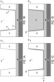
- FIGS. 1A-1D illustrate a first example simplified process sequence for forming a titanium contact to silicon germanium.
- FIG. 1A illustrates a structure 100 comprising a substrate 104, a silicon germanium (SiGe) layer 108, and isolation regions 112 in which a trench 116 has been formed by a suitable etch process.
- the substrate 104 can comprise silicon and can be a bulk silicon wafer, a silicon-on-insulator wafer, or another suitable substrate.
- the SiGe layer 108 comprises one or more p-type dopants, such as boron, indium, or gallium, or one or more n-type dopants, such as phosphorous, arsenic, or antimony.
- the SiGe layer 108 can be an epitaxially grown layer with doping of the SiGe layer 108 occurring during epitaxial growth of the layer 108 (e.g., in situ doping).
- the isolation regions 112 can comprise any suitable nitride or oxide, such as silicon dioxide (SiO 2 , which is a material that comprises silicon and oxygen), carbon-doped silicon dioxide (C-doped SiO 2 , also known as CDO or organosilicate glass, which is a material that comprises silicon, oxygen, and carbon), fluorine-doped silicon dioxide (F-doped SiO 2 , also known as fluorosilicate glass, which is a material that comprises fluorine, silicon, and oxygen), hydrogen-doped silicon dioxide (H-doped SiO 2 , which is a material that comprises silicon, oxygen, and hydrogen), or silicon nitride (Si 3 N 4 , which is a material that comprises silicon and nitrogen).
- silicon dioxide SiO 2
- C-doped SiO 2 also known as CDO or organosilicate glass, which is a material that comprises silicon, oxygen, and carbon
- fluorine-doped silicon dioxide F-doped SiO 2 , also known
- FIG. 1B illustrates the structure 100 after formation of a titanium layer 124.
- the titanium layer 124 can be formed by chemical vapor deposition (CVD), plasma enhanced chemical vapor deposition (PECVD), physical vapor deposition (e.g., such as sputtering), or other suitable deposition or other thin film formation processes.
- the titanium layer 124 is positioned adjacent to a portion of the silicon germanium layer 108 and sidewalls 114 of the isolation regions 112.
- FIG. 1C illustrates the structure 100 after formation of a titanium disilicide or titanium silicide layer 128 from the titanium layer 124.
- the terms titanium silicide and titanium disilicide are used interchangeably herein to refer to a material having the chemical composition TiSi 2 .
- the titanium layer 124 is exposed to a gaseous silicon precursor at an elevated temperature.
- the silicon precursor can be silane, disilane, trisilane, tetrasilane, or another suitable silicon precursor.
- the silicon precursor flows over the structure 100.
- the temperature of the chamber of a manufacturing tool in which the structure 100 is exposed to the silicon precursor is in the range of about 375-475 °C.
- the exposure of the titanium layer 124 to the silicon precursor can be performed in the same manufacturing tool (but in a different chamber) used for forming the titanium layer 124, thus allowing for an uninterrupted process flow between these two steps. That is, the structure 100 may not be removed from a semiconductor manufacturing tool between formation of the titanium layer 124 and transformation of the titanium layer 124 to titanium silicide.
- the titanium silicide layer 128 comprises an amount of unreacted titanium. That is, the titanium silicide layer 128 can comprise titanium that did not react with the silicon precursor to form titanium silicide.
- FIG. 1D illustrates the structure 100 after the trench 116 has been filled by a metal (trench metal) 132.
- the trench metal 132 can be formed by chemical vapor deposition (CVD), plasma enhanced chemical vapor deposition (PECVD), physical vapor deposition (e.g., such as sputtering), or other suitable fill process.
- the trench metal 132 can comprise tungsten, cobalt, titanium, gold, aluminum, molybdenum, chromium, and nickel, or another suitable metal or alloy.
- a barrier layer can be formed on the titanium silicide layer 128 before fill of the trench 116 by the trench metal 132, with the barrier layer positioned between the titanium silicide layer 128 and the trench metal 132, to protect the titanium silicide layer 128 from oxygen and other contaminants.
- a barrier layer can comprise tantalum (Ta), tantalum nitride (which is a material that comprises titanium and nitrogen (e.g., TaN, Ta 2 N, TasNs)), indium oxide (In 2 O 3 , which is a material that comprises indium and oxygen), tungsten nitride (which is a material that comprises tungsten and nitrogen (e.g., W 2 N, WN, WN 2 ), titanium nitride (TiN, which is a material that comprises titanium and nitrogen), ruthenium, or another suitable material.
- Ta tantalum nitride
- indium oxide In 2 O 3
- tungsten nitride which is a material that comprises tungsten and nitrogen
- TiN titanium nitride
- TiN which is a material that comprises titanium and nitrogen
- ruthenium or another suitable material.
- FIGS. 2A-2D illustrate a second example simplified process sequence for forming a titanium contact to silicon germanium.
- FIG. 2A illustrates a structure 200 comprising a substrate 204, a SiGe layer 208, and isolation regions 212 in which a trench 216 has been etched by a suitable etch process.
- a first titanium silicide layer 228 is positioned adjacent to sidewalls 214 of the isolation regions 212 and a portion of the silicon germanium layer 208.
- the layers and features of FIGS. 2A-2D can comprise the same materials as listed above for counterpart layers and features in FIGS. 1A-1D .
- the first titanium silicide layer 228 can have been formed in any of the manners described above for forming the titanium silicide layer 128 (e.g., through formation of a titanium layer subsequently exposed to a silicon precursor, such as silane, at an elevated temperature).
- FIG. 2B illustrates the structure 200 after the formation of a second titanium layer 232 positioned adjacent to the first titanium silicide layer 228.
- the second titanium layer 232 can be performed by any of the thin film layer formation processes described above for forming the titanium layer 124.
- FIG. 2C illustrates the structure 200 after formation of a second titanium silicide layer 236 from the second titanium layer 232. Formation of the second titanium silicide layer 236 from the second titanium layer 232 can be formed in any manner described above for forming the titanium silicide layer 128 from the titanium layer 124. In embodiments where multiple titanium silicide layers are formed as part of a contact formation process, the multiple titanium silicide layers can be considered to be a single titanium silicide layer with constituent titanium silicide sublayers.
- the structure 200 of FIGS. 2C-2D can be considered to have a single titanium silicide layer 230 with constituent titanium silicide sublayers 228 and 236.
- Individual titanium silicide layers may have variations in titanium and silicon concentration across the layer.
- a titanium silicide layer comprising multiple titanium silicide sublayers may have a repeating pattern of titanium and silicon concentration variations with the titanium and silicon concentration variations being repeated in the pattern being similar to that of a single titanium silicide layer.
- FIG. 2D illustrates the structure 200 after the trench 216 has been filled by a trench metal 240.
- the trench metal 240 can be formed by any of the fill processes described above for forming the trench metal 132.
- the trench metal 240 can comprise tungsten, cobalt, titanium, gold, aluminum, molybdenum, chromium, and nickel, or another suitable metal or alloy.
- a barrier layer can be formed on the second titanium silicide layer 236 before fill of the trench 216 and can be positioned between the second titanium silicide layer 236 and the trench metal 240.
- the barrier layer can comprise any of the barrier layer materials described above.
- FIGS. 2A-2D illustrate a titanium contact formation process where a cycle of titanium layer formation followed by titanium silicide layer formation is performed twice.
- the titanium layer formation-titanium silicide formation cycle can be performed three or more times.
- the same silicon precursor is used in forming the individual titanium silicide layers.
- the silicon precursor used in forming at least one of the titanium silicide layers is different than the silicon precursor used in forming the other titanium silicide layers.
- a different silicon precursor can be used in the formation of each titanium silicide layer.
- the thickness of the titanium silicide layer (e.g., thickness 140 of the titanium silicide layer 128) or the combined thickness of multiple titanium silicide layers (e.g., combined thickness 244 of the titanium silicide layers 228 and 236) is about 5-6 nm. In some embodiments, this thickness is about 2-6 nm.
- the individual titanium silicide layers may be thinner than those formed in titanium contact formation processes where only one titanium silicide layer is formed.
- the formation of titanium contacts formed by the titanium contact formation technologies herein can allow for titanium silicide layers thicknesses (e.g., thickness 140, 244) that are greater than titanium silicide layer thicknesses in titanium contacts formed by other approaches.
- Titanium contacts formed by the titanium contact formation technologies described herein can be thermally stable in that their contact resistance remains substantially unchanged after being subjected to subsequent annealing and other high-temperature processes.
- the thermal stability of the titanium contacts formed as described herein is understood to be at least the result of reduced interdiffusion between titanium and germanium across the titanium silicide-silicon germanium interface, which can reduce the creation of voids in the silicon germanium layer.
- the reduced interdiffusion is understood to be the result of a low amount (or no amount) of titanium in the titanium layer being left unreacted after formation of the titanium silicide layer.
- the formation of multiple titanium silicide layers may be advantageous in that less titanium in a thinner titanium layer may be left unreacted after the titanium silicide formation process than one in a process in which a single thicker titanium layer is formed.
- the titanium silicide formation processes described herein may form a purer form of titanium silicide relative to existing titanium contact formation processes. This may provide for a lower titanium silicide layer resistance if the purer titanium silicide layer comprises a single phase of titanium silicide.
- the titanium silicide layer may have a substantially uniform thickness and consistent electrical conductivity across the span of the titanium silicide-silicon germanium interface.
- the formation of titanium contacts using the technologies described herein may result in titanium silicide layers that have sharp interfaces with adjacent silicon germanium layers and trench metals due to a reduced amount of interdiffusion.
- the amount of germanium across a titanium silicide-silicon germanium boundary can decrease from a first germanium percentage concentration (e.g., 50% of the silicon germanium layer) on the silicon germanium layer-side of the boundary (e.g., boundaries 128-132, 228-240) to a second germanium percentage concentration of ten percent of the titanium silicide layer within 1.5 nm of the titanium silicide-silicon germanium boundary on the titanium silicide side of the boundary.
- a first germanium percentage concentration e.g., 50% of the silicon germanium layer
- the silicon germanium layer-side of the boundary e.g., boundaries 128-132, 228-240
- the amount of trench metal across a titanium silicide layer-trench metal layer boundary can decrease from a first metal percentage concentration (e.g., 50% or more of the trench metal layer) on the trench metal layer-side of the boundary (e.g., boundaries 128-108, 228-208) to a second trench metal percentage concentration of ten percent of the titanium silicide layer within 1.5 nm from the titanium silicide-silicon germanium boundary on the titanium silicide side of the boundary.
- a first metal percentage concentration e.g., 50% or more of the trench metal layer
- the second trench metal percentage concentration of ten percent of the titanium silicide layer within 1.5 nm from the titanium silicide-silicon germanium boundary on the titanium silicide side of the boundary.
- the silicon germanium layer (e.g., 108, 208) can be amorphized prior to formation of a titanium layer on the silicon germanium layer through the implantation of boron (e.g., boron-11) and germanium into the silicon germanium layer.
- boron e.g., boron-11
- another element or combination of elements can be implanted into a SiGe layer to amorphize a portion of the SiGe layer.
- the dose and energy of the implanted boron and germanium are such that a region of the silicon germanium layer extends from a surface of the silicon germanium layer to a depth within the silicon germanium layer is amorphized.
- Amorphization of the silicon germanium layer prior to formation of the titanium layer can aid in the robustness of the silicon germanium layer against microvoid growth during subsequent annealing and other high-temperature processes and can thus contribute to the thermal stability of the titanium contacts.
- titanium contacts illustrated in FIGS. 1A-1D and 2A-2D are discussed in the context of contacts to silicon germanium layers, in other embodiments, titanium contacts can be formed to a silicon layer or substrate, or another suitable semiconductor layer or substrate.
- the technologies for forming titanium contacts described herein can be utilized to form titanium contacts to SiGe layers that that are part of a source region or a drain region of a transistor, such as a planar FET, a FinFET, a gate-all-around FET (GAAFET), a stacked GAAFET, or another type of transistor.
- the titanium contact formation technologies disclosed herein can be utilized to form titanium contacts to a backside of a wafer (the side of a wafer opposite to the side of the wafer upon which a plurality of active devices (e.g., electronic transistors, spintronic devices) are located).
- the titanium contacts formed using the titanium contact formation technologies described herein can be used in any processor unit, integrated circuit component, or computing system described or referenced herein. Such titanium contacts can be fabricated as part of an integrated circuit structure.
- the integrated circuit structure can comprise a die substrate, such as a die substrate comprising silicon, and one or more interconnect or metal layers.
- a titanium contact formed as described herein can connect to a line of an interconnect or metal layer by a via or by being positioned adjacent to a line of a metal layer.
- the integrated circuit structure can comprise other types of devices, such as electronic transistors (transistors such as CMOS transistors that operate through control of the flow of electric current and that do not rely upon the switching of the magnetization of a layer or component for operation) and/or magnetoelectric spin-orbit (MESO) devices that use magnetoelectric switching to convert an input voltage/charge into a magnetic spin state (e.g., charge-to-spin conversion) and further uses spin-orbit transduction to convert the magnetic spin state back into an output charge/voltage (e.g., spin-to-charge conversion).
- An integrated circuit component comprising titanium contacts formed as described herein can be attached to a printed circuit board.
- one or more additional integrated circuit components can be attached to the circuit board.
- the printed circuit board and the integrated circuit component can be located in a computing device that comprises a housing that encloses the printed circuit board and the integrated circuit component.
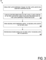
- FIG. 3 is an example method of forming a titanium contact.
- the method 300 can be performed by a semiconductor device manufacturer.
- a first layer comprising titanium is formed, the first layer located on a substrate comprising silicon.
- a silicon precursor flows over the first layer, at least a portion of the first layer after the silicon precursor flows over the first layer comprising titanium and silicon.
- a second layer is formed comprising a metal, the second layer located on the first layer.
- one or more annealing processes are performed on the first layer, the second layer, and the substrate.
- the method 300 can comprise additional elements.
- the silicon precursor of element 320 can be a first silicon precursor, the method 300 further comprising, after the first silicon precursor flows over the first layer and prior to forming the second layer: forming a third layer comprising titanium, the third layer positioned adjacent to the first layer; and flowing a second silicon precursor over the third layer, at least a portion of the third layer after flowing the silicon precursor over the second layer comprising titanium and silicon, the third layer located between the first layer and the second layer.
- the method can further comprise, after flowing the second silicon precursor over the third layer and prior to forming the second layer: forming a fourth layer comprising titanium, the fourth layer positioned adjacent to the third layer; and flowing a third silicon precursor over the fourth layer, at least a portion of the fourth layer after flowing the silicon precursor over the fourth layer comprising titanium and silicon, the third layer located between the first layer and the second layer.
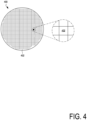
- FIG. 4 is a top view of a wafer 400 and dies 402 that may be included in any of the microelectronic assemblies disclosed herein.
- the wafer 400 may be composed of semiconductor material and may include one or more dies 402 having integrated circuit structures formed on a surface of the wafer 400.
- the individual dies 402 may be a repeating unit of an integrated circuit product that includes any suitable integrated circuit. After the fabrication of the semiconductor product is complete, the wafer 400 may undergo a singulation process in which the dies 402 are separated from one another to provide discrete "chips" of the integrated circuit product.
- the die 402 may include one or more transistors (e.g., some of the transistors 540 of FIG.
- the wafer 400 or the die 402 may include a memory device (e.g., a random access memory (RAM) device, such as a static RAM (SRAM) device, a magnetic RAM (MRAM) device, a resistive RAM (RRAM) device, a conductive-bridging RAM (CBRAM) device, etc.), a logic device (e.g., an AND, OR, NAND, or NOR gate), or any other suitable circuit element. Multiple ones of these devices may be combined on a single die 402.
- RAM random access memory
- SRAM static RAM
- MRAM magnetic RAM
- RRAM resistive RAM
- CBRAM conductive-bridging RAM
- a memory array formed by multiple memory devices may be formed on a same die 402 as a processor unit (e.g., the processor unit 802 of FIG. 8 ) or other logic that is configured to store information in the memory devices or execute instructions stored in the memory array.
- Various ones of the microelectronic assemblies disclosed herein may be manufactured using a die-to-wafer assembly technique in which some dies 502 are attached to a wafer 400 that include others of the dies 502, and the wafer 400 is subsequently singulated.
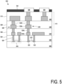
- FIG. 5 is a cross-sectional side view of an integrated circuit device 500 that may include titanium contacts according to the technologies disclosed herein.
- One or more of the integrated circuit devices 500 may be included in one or more dies 402 ( FIG. 4 ).
- the integrated circuit device 500 may be formed on a die substrate 502 (e.g., the wafer 400 of FIG. 4 ) and may be included in a die (e.g., the die 402 of FIG. 4 ).
- the die substrate 502 may be a semiconductor substrate composed of semiconductor material systems including, for example, n-type or p-type materials systems (or a combination of both).
- the die substrate 502 may include, for example, a crystalline substrate formed using a bulk silicon or a silicon-on-insulator (SOI) substructure.
- SOI silicon-on-insulator
- the die substrate 502 may be formed using alternative materials, which may or may not be combined with silicon, that include, but are not limited to, germanium, indium antimonide, lead telluride, indium arsenide, indium phosphide, gallium arsenide, or gallium antimonide. Further materials classified as group II-VI, III-V, or IV may also be used to form the die substrate 502. Although a few examples of materials from which the die substrate 502 may be formed are described here, any material that may serve as a foundation for an integrated circuit device 500 may be used.
- the die substrate 502 may be part of a singulated die (e.g., the dies 402 of FIG. 4 ) or a wafer (e.g., the wafer 400 of FIG. 4 ).
- the integrated circuit device 500 may include one or more device layers 504 disposed on the die substrate 502.
- the device layer 504 may include features of one or more transistors 540 (e.g., metal oxide semiconductor field-effect transistors (MOSFETs)) formed on the die substrate 502.
- the transistors 540 may include, for example, one or more source and/or drain (S/D) regions 520, a gate 522 to control current flow between the S/D regions 520, and one or more S/D contacts 524 to route electrical signals to/from the S/D regions 520.
- the S/D contacts 624 may be formed using any of the titanium contacts formation technologies described herein.
- the transistors 540 may include additional features not depicted for the sake of clarity, such as device isolation regions, gate contacts, and the like.
- the transistors 540 are not limited to the type and configuration depicted in FIG. 5 and may include a wide variety of other types and configurations such as, for example, planar transistors, non-planar transistors, or a combination of both.
- Non- planar transistors may include FinFET transistors, such as double-gate transistors or tri-gate transistors, and wrap-around or all-around gate transistors, such as nanoribbon, nanosheet, or nanowire transistors.
- FIGS. 6A-6D are perspective views of an example planar FET, FinFET, gate-all-around FET, and stacked gate-all-around FET.
- the transistors illustrated in FIGS. 6A-6D are formed on a substrate 616 having a surface 608. Isolation regions 614 separate the source and drain regions of the transistors from other transistors and from a bulk region 618 of the substrate 616.
- FIG. 6A is a perspective view of an example planar transistor 600 comprising a gate 602 that controls current flow between a source region 604 and a drain region 606.
- the transistor 600 is planar in that the source region 604 and the drain region 606 are planar with respect to the substrate surface 608.
- FIG. 6B is a perspective view of an example FinFET transistor 620 comprising a gate 622 that controls current flow between a source region 624 and a drain region 626.
- the transistor 620 is non-planar in that the source region 624 and the drain region 626 comprise "fins" that extend upwards from the substrate surface 628.
- the transistor 620 can be considered a tri-gate transistor.
- FIG. 6B illustrates one S/D fin extending through the gate 622, but multiple S/D fins can extend through the gate of a FinFET transistor.
- FIG. 6C is a perspective view of a gate-all-around (GAA) transistor 640 comprising a gate 642 that controls current flow between a source region 644 and a drain region 646.
- the transistor 640 is non-planar in that the source region 644 and the drain region 646 are elevated from the substrate surface 628.
- FIG. 6D is a perspective view of a GAA transistor 660 comprising a gate 662 that controls current flow between multiple elevated source regions 664 and multiple elevated drain regions 666.
- the transistor 660 is a stacked GAA transistor as the gate controls the flow of current between multiple elevated S/D regions stacked on top of each other.
- the transistors 640 and 660 are considered gate-all-around transistors as the gates encompass all sides of the semiconductor portions that extend from the source regions to the drain regions.
- the transistors 640 and 660 can alternatively be referred to as nanowire, nanosheet, or nanoribbon transistors depending on the width (e.g., widths 648 and 668 of transistors 640 and 660, respectively) of the semiconductor portions extending through the gate.
- a transistor 540 may include a gate 522 formed of at least two layers, a gate dielectric and a gate electrode.
- the gate dielectric may include one layer or a stack of layers.
- the one or more layers may include silicon oxide, silicon dioxide, silicon carbide, and/or a high-k dielectric material.
- the high-k dielectric material may include elements such as hafnium, silicon, oxygen, titanium, tantalum, lanthanum, aluminum, zirconium, barium, strontium, yttrium, lead, scandium, niobium, and zinc.
- high-k materials that may be used in the gate dielectric include, but are not limited to, hafnium oxide, hafnium silicon oxide, lanthanum oxide, lanthanum aluminum oxide, zirconium oxide, zirconium silicon oxide, tantalum oxide, titanium oxide, barium strontium titanium oxide, barium titanium oxide, strontium titanium oxide, yttrium oxide, aluminum oxide, lead scandium tantalum oxide, and lead zinc niobate.
- an annealing process may be carried out on the gate dielectric to improve its quality when a high-k material is used.
- the gate electrode may be formed on the gate dielectric and may include at least one p-type work function metal or n-type work function metal, depending on whether the transistor 540 is to be a p-type metal oxide semiconductor (PMOS) or an n-type metal oxide semiconductor (NMOS) transistor.
- the gate electrode may consist of a stack of two or more metal layers, where one or more metal layers are work function metal layers and at least one metal layer is a fill metal layer. Further metal layers may be included for other purposes, such as a barrier layer.
- metals that may be used for the gate electrode include, but are not limited to, ruthenium, palladium, platinum, cobalt, nickel, conductive metal oxides (e.g., ruthenium oxide), and any of the metals discussed below with reference to an NMOS transistor (e.g., for work function tuning).
- metals that may be used for the gate electrode include, but are not limited to, hafnium, zirconium, titanium, tantalum, aluminum, alloys of these metals, carbides of these metals (e.g., hafnium carbide, zirconium carbide, titanium carbide, tantalum carbide, and aluminum carbide), and any of the metals discussed above with reference to a PMOS transistor (e.g., for work function tuning).
- the gate electrode when viewed as a cross-section of the transistor 540 along the source-channel-drain direction, may consist of a U-shaped structure that includes a bottom portion substantially parallel to the surface of the die substrate 502 and two sidewall portions that are substantially perpendicular to the top surface of the die substrate 502.
- at least one of the metal layers that form the gate electrode may simply be a planar layer that is substantially parallel to the top surface of the die substrate 502 and does not include sidewall portions substantially perpendicular to the top surface of the die substrate 502.
- the gate electrode may consist of a combination of U-shaped structures and planar, non-U-shaped structures.
- the gate electrode may consist of one or more U-shaped metal layers formed atop one or more planar, non-U-shaped layers.
- a pair of sidewall spacers may be formed on opposing sides of the gate stack to bracket the gate stack.
- the sidewall spacers may be formed from materials such as silicon nitride, silicon oxide, silicon carbide, silicon nitride doped with carbon, and silicon oxynitride. Processes for forming sidewall spacers are well known in the art and generally include deposition and etching process steps. In some embodiments, a plurality of spacer pairs may be used; for instance, two pairs, three pairs, or four pairs of sidewall spacers may be formed on opposing sides of the gate stack.
- the S/D regions 520 may be formed within the die substrate 502 adjacent to the gate 522 of individual transistors 540.
- the S/D regions 520 may be formed using an implantation/diffusion process or an etching/deposition process, for example.
- dopants such as boron, aluminum, antimony, phosphorous, or arsenic may be ion-implanted into the die substrate 502 to form the S/D regions 520.
- An annealing process that activates the dopants and causes them to diffuse farther into the die substrate 502 may follow the ion-implantation process.
- the die substrate 502 may first be etched to form recesses at the locations of the S/D regions 520.
- the S/D regions 520 may be fabricated using a silicon alloy such as silicon germanium or silicon carbide.
- the epitaxially deposited silicon alloy may be doped in situ with dopants such as boron, arsenic, or phosphorous.
- the S/D regions 520 may be formed using one or more alternate semiconductor materials such as germanium or a group III-V material or alloy.
- one or more layers of metal and/or metal alloys may be used to form the S/D regions 520.
- Electrical signals such as power and/or input/output (I/O) signals, may be routed to and/or from the devices (e.g., transistors 540) of the device layer 504 through one or more interconnect layers disposed on the device layer 504 (illustrated in FIG. 5 as interconnect layers 506-510).
- interconnect layers 506-510 electrically conductive features of the device layer 504 (e.g., the gate 522 and the S/D contacts 524) may be electrically coupled with the interconnect structures 528 of the interconnect layers 506-510.
- the one or more interconnect layers 506-510 may form a metallization stack (also referred to as an "ILD stack") 519 of the integrated circuit device 500.
- the interconnect structures 528 may be arranged within the interconnect layers 506-510 to route electrical signals according to a wide variety of designs; in particular, the arrangement is not limited to the particular configuration of interconnect structures 528 depicted in FIG. 5 Although a particular number of interconnect layers 506-510 is depicted in FIG. 5 , embodiments of the present disclosure include integrated circuit devices having more or fewer interconnect layers than depicted.
- the interconnect structures 528 may include lines 528a and/or vias 528b filled with an electrically conductive material such as a metal.
- the lines 528a may be arranged to route electrical signals in a direction of a plane that is substantially parallel with a surface of the die substrate 502 upon which the device layer 504 is formed.
- the lines 528a may route electrical signals in a direction in and out of the page and/or in a direction across the page from the perspective of FIG. 7 .
- the vias 528b may be arranged to route electrical signals in a direction of a plane that is substantially perpendicular to the surface of the die substrate 502 upon which the device layer 504 is formed.
- the vias 528b may electrically couple lines 528a of different interconnect layers 506-510 together.
- the interconnect layers 506-510 may include a dielectric material 526 disposed between the interconnect structures 528, as shown in FIG. 5 .
- dielectric material 526 disposed between the interconnect structures 528 in different ones of the interconnect layers 506-510 may have different compositions; in other embodiments, the composition of the dielectric material 526 between different interconnect layers 506-510 may be the same.
- the device layer 504 may include a dielectric material 526 disposed between the transistors 540 and a bottom layer of the metallization stack as well.
- the dielectric material 526 included in the device layer 504 may have a different composition than the dielectric material 526 included in the interconnect layers 506-510; in other embodiments, the composition of the dielectric material 526 in the device layer 504 may be the same as a dielectric material 526 included in any one of the interconnect layers 506-510.
- a first interconnect layer 506 (referred to as Metal 1 or "M1") may be formed directly on the device layer 504.
- the first interconnect layer 506 may include lines 528a and/or vias 528b, as shown.
- the lines 528a of the first interconnect layer 506 may be coupled with contacts (e.g., the S/D contacts 524) of the device layer 504.
- the vias 528b of the first interconnect layer 506 may be coupled with the lines 528a of a second interconnect layer 508.
- the second interconnect layer 508 (referred to as Metal 2 or "M2”) may be formed directly on the first interconnect layer 506.
- the second interconnect layer 508 may include via 528b to couple the lines 528 of the second interconnect layer 508 with the lines 528a of a third interconnect layer 510.
- the lines 528a and the vias 528b are structurally delineated with a line within individual interconnect layers for the sake of clarity, the lines 528a and the vias 528b may be structurally and/or materially contiguous (e.g., simultaneously filled during a dual-damascene process) in some embodiments.
- the third interconnect layer 510 (referred to as Metal 3 or "M3") (and additional interconnect layers, as desired) may be formed in succession on the second interconnect layer 508 according to similar techniques and configurations described in connection with the second interconnect layer 508 or the first interconnect layer 506.
- the interconnect layers that are "higher up” in the metallization stack 519 in the integrated circuit device 500 i.e., farther away from the device layer 504 may be thicker that the interconnect layers that are lower in the metallization stack 519, with lines 528a and vias 528b in the higher interconnect layers being thicker than those in the lower interconnect layers.
- the integrated circuit device 500 may include a solder resist material 534 (e.g., polyimide or similar material) and one or more conductive contacts 536 formed on the interconnect layers 506-510.
- the conductive contacts 536 are illustrated as taking the form of bond pads.
- the conductive contacts 536 may be electrically coupled with the interconnect structures 528 and configured to route the electrical signals of the transistor(s) 540 to external devices.
- solder bonds may be formed on the one or more conductive contacts 536 to mechanically and/or electrically couple an integrated circuit die including the integrated circuit device 500 with another component (e.g., a printed circuit board).
- the integrated circuit device 500 may include additional or alternate structures to route the electrical signals from the interconnect layers 506-510; for example, the conductive contacts 536 may include other analogous features (e.g., posts) that route the electrical signals to external components.
- the integrated circuit device 500 may include another metallization stack (not shown) on the opposite side of the device layer(s) 504.
- This metallization stack may include multiple interconnect layers as discussed above with reference to the interconnect layers 506-510, to provide conductive pathways (e.g., including conductive lines and vias) between the device layer(s) 504 and additional conductive contacts (not shown) on the opposite side of the integrated circuit device 500 from the conductive contacts 536.
- the integrated circuit device 500 may include one or more through silicon vias (TSVs) through the die substrate 502; these TSVs may make contact with the device layer(s) 504, and may provide conductive pathways between the device layer(s) 504 and additional conductive contacts (not shown) on the opposite side of the integrated circuit device 500 from the conductive contacts 536.
- TSVs through silicon vias
- TSVs extending through the substrate can be used for routing power and ground signals from conductive contacts on the opposite side of the integrated circuit device 500 from the conductive contacts 536 to the transistors 540 and any other components integrated into the die 500, and the metallization stack 519 can be used to route I/O signals from the conductive contacts 536 to transistors 540 and any other components integrated into the die 500.
- Multiple integrated circuit devices 500 may be stacked with one or more TSVs in the individual stacked devices providing connection between one of the devices to any of the other devices in the stack.
- one or more high-bandwidth memory (HBM) integrated circuit dies can be stacked on top of a base integrated circuit die and TSVs in the HBM dies can provide connection between the individual HBM and the base integrated circuit die.
- Conductive contacts can provide additional connections between adjacent integrated circuit dies in the stack.
- the conductive contacts can be fine-pitch solder bumps (microbumps).
- FIG. 7 is a cross-sectional side view of an integrated circuit device assembly 700 that may include any of the microelectronic assemblies disclosed herein.
- the integrated circuit device assembly 700 includes a number of components disposed on a circuit board 702 (which may be a motherboard, system board, mainboard, etc.).
- the integrated circuit device assembly 700 includes components disposed on a first face 740 of the circuit board 702 and an opposing second face 742 of the circuit board 702; generally, components may be disposed on one or both faces 740 and 742.
- Any of the integrated circuit components discussed below with reference to the integrated circuit device assembly 700 may take the form of any suitable ones of the embodiments of the microelectronic assemblies disclosed herein.
- the circuit board 702 may be a printed circuit board (PCB) including multiple metal (or interconnect) layers separated from one another by layers of dielectric material and interconnected by electrically conductive vias.
- the individual metal layers comprise conductive traces. Any one or more of the metal layers may be formed in a desired circuit pattern to route electrical signals (optionally in conjunction with other metal layers) between the components coupled to the circuit board 702.
- the circuit board 702 may be a non-PCB substrate.
- the integrated circuit device assembly 700 illustrated in FIG. 7 includes a package-on-interposer structure 736 coupled to the first face 740 of the circuit board 702 by coupling components 716.
- the coupling components 716 may electrically and mechanically couple the package-on-interposer structure 736 to the circuit board 702, and may include solder balls (as shown in FIG. 7 ), pins (e.g., as part of a pin grid array (PGA), contacts (e.g., as part of a land grid array (LGA)), male and female portions of a socket, an adhesive, an underfill material, and/or any other suitable electrical and/or mechanical coupling structure.
- the coupling components 716 may serve as the coupling components illustrated or described for any of the substrate assembly or substrate assembly components described herein, as appropriate.
- the package-on-interposer structure 736 may include an integrated circuit component 720 coupled to an interposer 704 by coupling components 718.
- the coupling components 718 may take any suitable form for the application, such as the forms discussed above with reference to the coupling components 716. Although a single integrated circuit component 720 is shown in FIG. 7 , multiple integrated circuit components may be coupled to the interposer 704; indeed, additional interposers may be coupled to the interposer 704.
- the interposer 704 may provide an intervening substrate used to bridge the circuit board 702 and the integrated circuit component 720.
- the integrated circuit component 720 may be a packaged or unpacked integrated circuit product that includes one or more integrated circuit dies (e.g., the die 402 of FIG. 4 , the integrated circuit device 500 of FIG. 5 ) and/or one or more other suitable components.
- a packaged integrated circuit component comprises one or more integrated circuit dies mounted on a package substrate with the integrated circuit dies and package substrate encapsulated in a casing material, such as a metal, plastic, glass, or ceramic.
- a single monolithic integrated circuit die comprises solder bumps attached to contacts on the die. The solder bumps allow the die to be directly attached to the interposer 704.
- the integrated circuit component 720 can comprise one or more computing system components, such as one or more processor units (e.g., system-on-a-chip (SoC), processor core, graphics processor unit (GPU), accelerator, chipset processor), I/O controller, memory, or network interface controller.
- processor units e.g., system-on-a-chip (SoC)
- SoC system-on-a-chip
- GPU graphics processor unit
- accelerator chipset processor
- I/O controller I/O controller
- memory or network interface controller.
- the integrated circuit component 720 can comprise one or more additional active or passive devices such as capacitors, decoupling capacitors, resistors, inductors, fuses, diodes, transformers, sensors, electrostatic discharge (ESD) devices, and memory devices.
- ESD electrostatic discharge
- the integrated circuit component 720 comprises multiple integrated circuit dies
- they dies can be of the same type (a homogeneous multi-die integrated circuit component) or of two or more different types (a heterogeneous multi-die integrated circuit component).
- a multi-die integrated circuit component can be referred to as a multi-chip package (MCP) or multi-chip module (MCM).
- the integrated circuit component 720 can comprise additional components, such as embedded DRAM, stacked high bandwidth memory (HBM), shared cache memories, input/output (I/O) controllers, or memory controllers. Any of these additional components can be located on the same integrated circuit die as a processor unit, or on one or more integrated circuit dies separate from the integrated circuit dies comprising the processor units. These separate integrated circuit dies can be referred to as "chiplets". In embodiments where an integrated circuit component comprises multiple integrated circuit dies, interconnections between dies can be provided by the package substrate, one or more silicon interposers, one or more silicon bridges embedded in the package substrate (such as Intel ® embedded multi-die interconnect bridges (EMIBs)), or combinations thereof.
- EMIBs Intel ® embedded multi-die interconnect bridges
- the interposer 704 may spread connections to a wider pitch or reroute a connection to a different connection.
- the interposer 704 may couple the integrated circuit component 720 to a set of ball grid array (BGA) conductive contacts of the coupling components 716 for coupling to the circuit board 702.
- BGA ball grid array
- the integrated circuit component 720 and the circuit board 702 are attached to opposing sides of the interposer 704; in other embodiments, the integrated circuit component 720 and the circuit board 702 may be attached to a same side of the interposer 704.
- three or more components may be interconnected by way of the interposer 704.
- the interposer 704 may be formed as a PCB, including multiple metal layers separated from one another by layers of dielectric material and interconnected by electrically conductive vias.
- the interposer 704 may be formed of an epoxy resin, a fiberglass-reinforced epoxy resin, an epoxy resin with inorganic fillers, a ceramic material, or a polymer material such as polyimide.
- the interposer 704 may be formed of alternate rigid or flexible materials that may include the same materials described above for use in a semiconductor substrate, such as silicon, germanium, and other group III-V and group IV materials.
- the interposer 704 may include metal interconnects 708 and vias 710, including but not limited to through hole vias 710-1 (that extend from a first face 750 of the interposer 704 to a second face 754 of the interposer 704), blind vias 710-2 (that extend from the first or second faces 750 or 754 of the interposer 704 to an internal metal layer), and buried vias 710-3 (that connect internal metal layers).
- through hole vias 710-1 that extend from a first face 750 of the interposer 704 to a second face 754 of the interposer 704
- blind vias 710-2 that extend from the first or second faces 750 or 754 of the interposer 704 to an internal metal layer
- buried vias 710-3 that connect internal metal layers.
- the interposer 704 can comprise a silicon interposer. Through silicon vias (TSV) extending through the silicon interposer can connect connections on a first face of a silicon interposer to an opposing second face of the silicon interposer.
- TSV through silicon vias
- an interposer 704 comprising a silicon interposer can further comprise one or more routing layers to route connections on a first face of the interposer 704 to an opposing second face of the interposer 704.
- the interposer 704 may further include embedded devices 714, including both passive and active devices. Such devices may include, but are not limited to, capacitors, decoupling capacitors, resistors, inductors, fuses, diodes, transformers, sensors, electrostatic discharge (ESD) devices, and memory devices. More complex devices such as radio frequency devices, power amplifiers, power management devices, antennas, arrays, sensors, and microelectromechanical systems (MEMS) devices may also be formed on the interposer 704.
- the package-on-interposer structure 736 may take the form of any of the package-on-interposer structures known in the art. In embodiments where the interposer is a non-printed circuit board
- the integrated circuit device assembly 700 may include an integrated circuit component 724 coupled to the first face 740 of the circuit board 702 by coupling components 722.
- the coupling components 722 may take the form of any of the embodiments discussed above with reference to the coupling components 716
- the integrated circuit component 724 may take the form of any of the embodiments discussed above with reference to the integrated circuit component 720.
- the integrated circuit device assembly 700 illustrated in FIG. 7 includes a package-on-package structure 734 coupled to the second face 742 of the circuit board 702 by coupling components 728.
- the package-on-package structure 734 may include an integrated circuit component 726 and an integrated circuit component 732 coupled together by coupling components 730 such that the integrated circuit component 726 is disposed between the circuit board 702 and the integrated circuit component 732.
- the coupling components 728 and 730 may take the form of any of the embodiments of the coupling components 716 discussed above, and the integrated circuit components 726 and 732 may take the form of any of the embodiments of the integrated circuit component 720 discussed above.
- the package-on-package structure 734 may be configured in accordance with any of the package-on-package structures known in the art.
- FIG. 8 is a block diagram of an example electrical device 800 that may include an integrated circuit component comprising titanium contacts formed according to the technologies disclosed herein.
- any suitable ones of the components of the electrical device 800 may include one or more of the integrated circuit device assemblies 700, integrated circuit components 720, integrated circuit devices 500, or integrated circuit dies 402 disclosed herein, and may be arranged in any of the microelectronic assemblies disclosed herein.
- a number of components are illustrated in FIG. 8 as included in the electrical device 800, but any one or more of these components may be omitted or duplicated, as suitable for the application.
- some or all of the components included in the electrical device 800 may be attached to one or more motherboards mainboards, or system boards.
- one or more of these components are fabricated onto a single system-on-a-chip (SoC) die.
- SoC system-on-a-chip
- the electrical device 800 may not include one or more of the components illustrated in FIG. 8 , but the electrical device 800 may include interface circuitry for coupling to the one or more components.
- the electrical device 800 may not include a display device 806, but may include display device interface circuitry (e.g., a connector and driver circuitry) to which a display device 806 may be coupled.
- the electrical device 800 may not include an audio input device 824 or an audio output device 808, but may include audio input or output device interface circuitry (e.g., connectors and supporting circuitry) to which an audio input device 824 or audio output device 808 may be coupled.
- the electrical device 800 may include one or more processor units 802 (e.g., one or more processor units).
- processor unit e.g., one or more processor units
- processor unit may refer to any device or portion of a device that processes electronic data from registers and/or memory to transform that electronic data into other electronic data that may be stored in registers and/or memory.
- the processor unit 802 may include one or more digital signal processors (DSPs), application-specific integrated circuits (ASICs), central processing units (CPUs), graphics processing units (GPUs), general-purpose GPUs (GPGPUs), accelerated processing units (APUs), field-programmable gate arrays (FPGAs), neural network processing units (NPUs), data processor units (DPUs), accelerators (e.g., graphics accelerator, compression accelerator, artificial intelligence accelerator), controller cryptoprocessors (specialized processors that execute cryptographic algorithms within hardware), server processors, controllers, or any other suitable type of processor units.
- DSPs digital signal processors
- ASICs application-specific integrated circuits
- CPUs central processing units
- GPUs graphics processing units
- GPUs general-purpose GPUs
- APUs accelerated processing units
- FPGAs field-programmable gate arrays
- NPUs neural network processing units
- DPUs data processor units
- accelerators e.g., graphics accelerator, compression accelerator, artificial intelligence accelerator
- controller cryptoprocessors
- the electrical device 800 may include a memory 804, which may itself include one or more memory devices such as volatile memory (e.g., dynamic random access memory (DRAM), static random-access memory (SRAM)), non-volatile memory (e.g., read-only memory (ROM), flash memory, chalcogenide-based phase-change non-voltage memories), solid state memory, and/or a hard drive.
- volatile memory e.g., dynamic random access memory (DRAM), static random-access memory (SRAM)
- non-volatile memory e.g., read-only memory (ROM), flash memory, chalcogenide-based phase-change non-voltage memories
- solid state memory e.g., solid state memory, and/or a hard drive.
- the memory 804 may include memory that is located on the same integrated circuit die as the processor unit 802.
- This memory may be used as cache memory (e.g., Level 1 (L1), Level 2 (L2), Level 3 (L3), Level 4 (L4), Last Level Cache (LLC)) and may include embedded dynamic random access memory (eDRAM) or spin transfer torque magnetic random access memory (STT-MRAM).
- eDRAM embedded dynamic random access memory
- STT-MRAM spin transfer torque magnetic random access memory
- the electrical device 800 can comprise one or more processor units 802 that are heterogeneous or asymmetric to another processor unit 802 in the electrical device 800.
- processor units 802 can be a variety of differences between the processing units 802 in a system in terms of a spectrum of metrics of merit including architectural, microarchitectural, thermal, power consumption characteristics, and the like. These differences can effectively manifest themselves as asymmetry and heterogeneity among the processor units 802 in the electrical device 800.
- the electrical device 800 may include a communication component 812 (e.g., one or more communication components).
- the communication component 812 can manage wireless communications for the transfer of data to and from the electrical device 800.
- the term “wireless” and its derivatives may be used to describe circuits, devices, systems, methods, techniques, communications channels, etc., that may communicate data through the use of modulated electromagnetic radiation through a nonsolid medium.
- the term “wireless” does not imply that the associated devices do not contain any wires, although in some embodiments they might not.
- the communication component 812 may implement any of a number of wireless standards or protocols, including but not limited to Institute for Electrical and Electronic Engineers (IEEE) standards including Wi-Fi (IEEE 802.11 family), IEEE 802.16 standards (e.g., IEEE 802.16-2005 Amendment), Long-Term Evolution (LTE) project along with any amendments, updates, and/or revisions (e.g., advanced LTE project, ultra mobile broadband (UMB) project (also referred to as "3GPP2”), etc.).
- IEEE 802.16 compatible Broadband Wireless Access (BWA) networks are generally referred to as WiMAX networks, an acronym that stands for Worldwide Interoperability for Microwave Access, which is a certification mark for products that pass conformity and interoperability tests for the IEEE 802.16 standards.
- the communication component 812 may operate in accordance with a Global System for Mobile Communication (GSM), General Packet Radio Service (GPRS), Universal Mobile Telecommunications System (UMTS), High Speed Packet Access (HSPA), Evolved HSPA (E-HSPA), or LTE network.
- GSM Global System for Mobile Communication
- GPRS General Packet Radio Service
- UMTS Universal Mobile Telecommunications System
- High Speed Packet Access HSPA
- E-HSPA Evolved HSPA
- LTE LTE network.
- the communication component 812 may operate in accordance with Enhanced Data for GSM Evolution (EDGE), GSM EDGE Radio Access Network (GERAN), Universal Terrestrial Radio Access Network (UTRAN), or Evolved UTRAN (E-UTRAN).
- EDGE Enhanced Data for GSM Evolution
- GERAN GSM EDGE Radio Access Network
- UTRAN Universal Terrestrial Radio Access Network
- E-UTRAN Evolved UTRAN
- the communication component 812 may operate in accordance with Code Division Multiple Access (CDMA), Time Division Multiple Access (TDMA), Digital Enhanced Cordless Telecommunications (DECT), Evolution-Data Optimized (EV-DO), and derivatives thereof, as well as any other wireless protocols that are designated as 3G, 4G, 5G, and beyond.
- CDMA Code Division Multiple Access
- TDMA Time Division Multiple Access
- DECT Digital Enhanced Cordless Telecommunications
- EV-DO Evolution-Data Optimized
- the electrical device 800 may include an antenna 822 to facilitate wireless communications and/or to receive other wireless communications (such as AM or FM radio transmissions).
- the communication component 812 may manage wired communications, such as electrical, optical, or any other suitable communication protocols (e.g., IEEE 802.3 Ethernet standards).
- the communication component 812 may include multiple communication components. For instance, a first communication component 812 may be dedicated to shorter-range wireless communications such as Wi-Fi or Bluetooth, and a second communication component 812 may be dedicated to longer-range wireless communications such as global positioning system (GPS), EDGE, GPRS, CDMA, WiMAX, LTE, EV-DO, or others.
- GPS global positioning system
- EDGE EDGE
- GPRS long-range wireless communications
- CDMA Code Division Multiple Access
- WiMAX Code Division Multiple Access
- LTE Long Term Evolution
- EV-DO Evolution-DO
- the electrical device 800 may include battery/power circuitry 814.
- the battery/power circuitry 814 may include one or more energy storage devices (e.g., batteries or capacitors) and/or circuitry for coupling components of the electrical device 800 to an energy source separate from the electrical device 800 (e.g., AC line power).
- the electrical device 800 may include a display device 806 (or corresponding interface circuitry, as discussed above).
- the display device 806 may include one or more embedded or wired or wirelessly connected external visual indicators, such as a heads-up display, a computer monitor, a projector, a touchscreen display, a liquid crystal display (LCD), a light-emitting diode display, or a flat panel display.
- the electrical device 800 may include an audio output device 808 (or corresponding interface circuitry, as discussed above).
- the audio output device 808 may include any embedded or wired or wirelessly connected external device that generates an audible indicator, such speakers, headsets, or earbuds.
- the electrical device 800 may include an audio input device 824 (or corresponding interface circuitry, as discussed above).
- the audio input device 824 may include any embedded or wired or wirelessly connected device that generates a signal representative of a sound, such as microphones, microphone arrays, or digital instruments (e.g., instruments having a musical instrument digital interface (MIDI) output).
- the electrical device 800 may include a Global Navigation Satellite System (GNSS) device 818 (or corresponding interface circuitry, as discussed above), such as a Global Positioning System (GPS) device.
- GNSS Global Navigation Satellite System
- GPS Global Positioning System
- the GNSS device 818 may be in communication with a satellite-based system and may determine a geolocation of the electrical device 800 based on information received from one or more GNSS satellites, as known in the art.
- the electrical device 800 may include an other output device 810 (or corresponding interface circuitry, as discussed above).
- Examples of the other output device 810 may include an audio codec, a video codec, a printer, a wired or wireless transmitter for providing information to other devices, or an additional storage device.
- the electrical device 800 may include an other input device 820 (or corresponding interface circuitry, as discussed above).
- the other input device 820 may include an accelerometer, a gyroscope, a compass, an image capture device (e.g., monoscopic or stereoscopic camera), a trackball, a trackpad, a touchpad, a keyboard, a cursor control device such as a mouse, a stylus, a touchscreen, proximity sensor, microphone, a bar code reader, a Quick Response (QR) code reader, electrocardiogram (ECG) sensor, PPG (photoplethysmogram) sensor, galvanic skin response sensor, any other sensor, or a radio frequency identification (RFID) reader.
- an accelerometer e.g., a gyroscope, a compass
- an image capture device e.g., monoscopic or stereoscopic camera
- a trackball e.g., monoscopic or stereoscopic camera
- a trackball e.g
- the electrical device 800 may have any desired form factor, such as a hand-held or mobile electrical device (e.g., a cell phone, a smart phone, a mobile internet device, a music player, a tablet computer, a laptop computer, a 2-in-1 convertible computer, a portable all-in-one computer, a netbook computer, an ultrabook computer, a personal digital assistant (PDA), an ultra mobile personal computer, a portable gaming console, etc.), a desktop electrical device, a server, a rack-level computing solution (e.g., blade, tray or sled computing systems), a workstation or other networked computing component, a printer, a scanner, a monitor, a set-top box, an entertainment control unit, a stationary gaming console, smart television, a vehicle control unit, a digital camera, a digital video recorder, a wearable electrical device or an embedded computing system (e.g., computing systems that are part of a vehicle, smart home appliance, consumer electronics product or equipment, manufacturing equipment).
- the electrical device 800 may be any other electronic device that processes data.
- the electrical device 800 may comprise multiple discrete physical components. Given the range of devices that the electrical device 800 can be manifested as in various embodiments, in some embodiments, the electrical device 800 can be referred to as a computing device or a computing system.
- a list of items joined by the term “and/or” can mean any combination of the listed items.
- the phrase “A, B and/or C” can mean A; B; C; A and B; A and C; B and C; or A, B and C.
- a list of items joined by the term “at least one of” can mean any combination of the listed terms.
- the phrase “at least one of A, B or C” can mean A; B; C; A and B; A and C; B and C; or A, B, and C.
- a list of items joined by the term "one or more of” can mean any combination of the listed terms.
- the phrase “one or more of A, B and C” can mean A; B; C; A and B; A and C; B and C; or A, B, and C.
- a list of items stated or recited as having a trait, feature, etc. preceded by the word “individual” or “respective” means that all of the items in the list possess the stated or recited trait, feature, etc.
- the phrase “individual of A, B, or C, comprise a sidewall” or “respective of A, B, or C, comprise a sidewall” means that A comprises a sidewall, B comprises sidewall, and C comprises a sidewall.
Landscapes
- Chemical & Material Sciences (AREA)
- Inorganic Chemistry (AREA)
- Chemical Kinetics & Catalysis (AREA)
- Engineering & Computer Science (AREA)
- Materials Engineering (AREA)
- Mechanical Engineering (AREA)
- Metallurgy (AREA)
- Organic Chemistry (AREA)
- General Chemical & Material Sciences (AREA)
- Electrodes Of Semiconductors (AREA)
Description
- Titanium contacts can be used to provide electrically conductive connections to silicon germanium (SiGe) or silicon source/drain regions of field-effect transistors. Titanium contacts have an associated parasitic resistance that, if large enough, can affect transistor performance.
-
US 2020/098572 A1 discloses a method of forming a semiconductor device including forming a source/drain region on a substrate, depositing a metal-rich metal silicide layer on the source/drain region, depositing a silicon-rich metal silicide layer on the metal-rich metal silicide layer, and forming a contact plug on the silicon-rich metal silicide layer. This disclosure also describes a semiconductor device including a fin structure on a substrate, a source/drain region on the fin structure, a metal-rich metal silicide layer on the source/drain region, a silicon-rich metal silicide layer on the metal-rich metal silicide layer, and a contact plug on the silicon-rich metal silicide layer. -
EP 1 063 686 A2 discloses a method of forming a silicide layer in contact with a silicon substrate. The method comprises forming the silicide layer by supplying a silicon-containing source that is different from the silicon substrate, such that the silicon in the silicide layer originates primarily from the silicon-containing source. -
US 6 174 805 B1 discloses a titanium film forming method. Before a titanium film is formed, the temperature in a reaction chamber for forming the titanium film is set to a temperature or more at which hydrogen chloride is produced by chlorine and hydrogen. A hydrogenated gas is then fed into the reaction chamber for a predetermined period of time. With this process, before the titanium film is formed, chlorine gas and titanium chloride gas left in the reaction chamber for forming the titanium film are reduced. -
US 7 407 882 B1 discloses a method for manufacturing the semiconductor component. A layer of dielectric material is formed over a semiconductor substrate. An opening having sidewalls is formed in the dielectric layer and exposes a portion of the semiconductor substrate. Titanium silicide is disposed on the dielectric layer, sidewalls, and the exposed portion of the semiconductor substrate. The titanium silicide may be formed by disposing titanium on the dielectric layer, sidewalls, and exposed portion of the semiconductor substrate and reacting the titanium with silane. Alternatively, the titanium silicide may be sputter deposited. A layer of titanium nitride is formed on the titanium silicide. A layer of tungsten is formed on the titanium nitride. The tungsten, titanium nitride, and titanium silicide are polished to form the contact structures. -
US 2002/043722 A1 discloses a method comprising the steps of: (a) forming an insulating film on a semiconductor substrate on which an element is formed; (b) selectively removing a predetermined region of the insulating film to form an opening portion so as to expose an underlying conductive layer; (c) depositing a refractory metal on the opening portion; (d) depositing refractory metal silicide on the refractory metal deposited on the opening portion; and (e) filling the opening portion by depositing a refractory nitride metal on the refractory metal silicide deposited on the opening portion. -
-
FIGS. 1A-1D illustrate a first example simplified process sequence for forming a titanium contact to silicon germanium. -
FIGS. 2A-2D illustrate a second example simplified process sequence for forming a titanium contact to silicon germanium. -
FIG. 3 is an example method of forming a titanium contact. -
FIG. 4 is a top view of a wafer and dies that may be included in a microelectronic assembly, in accordance with any of the embodiments disclosed herein. -
FIG. 5 is a cross-sectional side view of anintegrated circuit device 500 that may include titanium contacts according to the technologies disclosed herein. -
FIGS. 6A-6D are perspective views of an example planar FET, FinFET, gate-all-around FET, and stacked gate-all-around FET. -
FIG. 7 is a cross-sectional side view of an integrated circuit device assembly that may include a microelectronic assembly, in accordance with any of the embodiments disclosed herein. -
FIG. 8 is a block diagram of an example electrical device that may include a microelectronic assembly, in accordance with any of the embodiments disclosed herein. - The source/drain regions of PMOSFETs (p-type metal-oxide-silicon field-effect transistors (FETs)) can comprise p-type silicon germanium (SiGe) layers epitaxially grown on a bulk silicon, silicon-on-insulator or another suitable substrate. Silicon germanium source/drain regions can introduce strain into the channel region of a MOSFET and the induced strain can cause the silicon atoms in the channel to stretch further apart than they would be in the absence of strain. This increased atomic spacing results in increased charge carrier mobility in the channel region, which can translate into increased transistor drive current.
- The formation of a titanium contact to a silicon germanium layer can comprise the formation of a titanium silicide layer positioned adjacent to the silicon germanium layer. The titanium silicide aids in forming a titanium contact with low electrical resistance. In existing processes, the titanium silicide can be formed using a salicide process in which the silicon used to form the titanium silicide comes from the silicon germanium layer.
- Titanium contacts formed via a process that comprises forming a titanium layer on crystalline silicon germanium can be thermally unstable in that their resistance (contact resistance) increases after being subjected to subsequent annealing and other high-temperature processing steps that occur in a semiconductor device manufacturing process after contact formation. The back end of line (BEOL) portion of a semiconductor device manufacturing process can involve numerous annealing and other high-temperature processing steps, the cumulative effect of which can cause titanium contact resistance to increase by more than 50% in some cases. The creation of voids in the silicon germanium layer at the titanium silicide-silicon germanium interface during the annealing and other high-temperature processing steps is understood to be at least partially responsible for titanium contact thermal instability. The increased resistance of titanium contacts due to their thermal instability can impact the performance of transistors having silicon germanium layer source/drain regions.
- Described herein are titanium contacts in which contact formation comprises the formation of a titanium silicide layer from a titanium layer in which the silicon for the titanium silicide layer is provided by exposure of the titanium layer to a silicon precursor, such as silane (disilane, trisilane, etc.) at an elevated temperature. A titanium silicide layer formed as such can help limit the amount of titanium and germanium interdiffusion that can occur at the titanium silicide-silicon germanium interface (and the resulting formation of voids in the silicon germanium layer) during subsequent annealing and other high-temperature processing steps. A titanium silicide formation process that does not scavenge silicon from a silicon germanium layer adjacent to a titanium layer can further reduce the creation of voids in the silicon germanium. Moreover, a surface region of a silicon germanium layer upon which a titanium layer is formed as part of a contact formation process can be preamorphized via boron and germanium implantation to further improve the robustness of the SiGe layer against microvoid development in subsequent annealing processing steps. The titanium contacts formed as described herein are thermally stable in that their resistance remains substantially unchanged after being subjected to downstream annealing and other high-temperature processes.
- In the following description, specific details are set forth, but embodiments of the technologies described herein may be practiced without these specific details. Well-known circuits, structures, and techniques have not been shown in detail to avoid obscuring an understanding of this description. Phrases such as "an embodiment," "various embodiments," "some embodiments," and the like may include features, structures, or characteristics, but not every embodiment necessarily includes the particular features, structures, or characteristics.
- Some embodiments may have some, all, or none of the features described for other embodiments. "First," "second," "third," and the like describe a common object and indicate different instances of like objects being referred to. Such adjectives do not imply objects so described must be in a given sequence, either temporally or spatially, in ranking, or any other manner. "Connected" may indicate elements are in direct physical or electrical contact with each other and "coupled" may indicate elements co-operate or interact with each other, but they may or may not be in direct physical or electrical contact. Furthermore, the terms "comprising," "including," "having," and the like, as used with respect to embodiments of the present disclosure, are synonymous. synonymous.
- Terms modified by the word "substantially" include arrangements, orientations, spacings, or positions that vary slightly from the meaning of the unmodified term. For example, the portion of a first layer or feature that is substantially perpendicular to a second layer or feature can include a first layer or feature that is +/- 20 degrees from a second layer or feature, a first surface that is substantially parallel to a second surface can include a first surface that is within several degrees of parallel from the second surface, a volume that is substantially filled by a via can comprise voids in the via, and a first edge that is substantially aligned with a second edge can be misaligned on the order of ones of nanometers, a contact resistance value that is substantially unchanged after one or more annealing processes include contact resistance values that change by 5% or less relative to their value prior to being subjected to one or more annealing processes. As used herein, the term "about" in reference to a value of a feature (e.g., height, width, spacing) or upper and lower limits of a range of values for a feature includes features values that are within several percent of the stated feature value, feature value lower range limit, or feature value upper range limit.
- In the following description, for purposes of explanation, numerous specific details are set forth in order to provide a thorough understanding thereof.
- As used herein, the phrase "located on" in the context of a first layer or component located on a second layer or component refers to the first layer or component being directly physically attached to the second part or component (no layers or components between the first and second layers or components) or physically attached to the second layer or component with one or more intervening layers or components. For example, with reference to
FIG. 1D , thetrench metal 132 is located on thetitanium silicide layer 128 whether thetrench metal 132 is directly physically attached to thetitanium silicide layer 128 or if there is an intervening layer (not shown inFIG. 1D ), such as a barrier layer. In another example, with reference toFIG. 1B , thetitanium layer 124 is located on thesubstrate 104, with an interveningsilicon germanium layer 108. - As used herein, the term "adjacent" refers to layers or components that are in physical contact with each other. That is, there is no layer or component between the stated adjacent layers or components. For example, a layer X that is adjacent to a layer Y refers to a layer that is in physical contact with layer Y.
- As used herein, the term "integrated circuit component" refers to a packaged or unpacked integrated circuit product. A packaged integrated circuit component comprises one or more integrated circuit dies mounted on a package substrate with the integrated circuit dies and package substrate encapsulated in a casing material, such as a metal, plastic, glass, or ceramic. In one example, a packaged integrated circuit component contains one or more processor units mounted on a substrate with an exterior surface of the substrate comprising a solder ball grid array (BGA). In one example of an unpackaged integrated circuit component, a single monolithic integrated circuit die comprises solder bumps attached to contacts on the die. The solder bumps allow the die to be directly attached to a printed circuit board. An integrated circuit component can comprise one or more of any computing system component described or referenced herein or any other computing system component, such as a processor unit (e.g., system-on-a-chip (SoC), processor core, graphics processor unit (GPU), accelerator, chipset processor), I/O controller, memory, or network interface controller.
- Reference is now made to the drawings, which are not necessarily drawn to scale, wherein similar or same numbers may be used to designate same or similar parts in different figures. The use of similar or same numbers in different figures does not mean all figures including similar or same numbers constitute a single or same embodiment. Like numerals having different letter suffixes may represent different instances of similar components. The drawings illustrate generally, by way of example, but not by way of limitation, various embodiments discussed in the present document.
-
FIGS. 1A-1D illustrate a first example simplified process sequence for forming a titanium contact to silicon germanium.FIG. 1A illustrates astructure 100 comprising asubstrate 104, a silicon germanium (SiGe)layer 108, andisolation regions 112 in which atrench 116 has been formed by a suitable etch process. Thesubstrate 104 can comprise silicon and can be a bulk silicon wafer, a silicon-on-insulator wafer, or another suitable substrate. In some embodiments, theSiGe layer 108 comprises one or more p-type dopants, such as boron, indium, or gallium, or one or more n-type dopants, such as phosphorous, arsenic, or antimony. In some embodiments, theSiGe layer 108 can be an epitaxially grown layer with doping of theSiGe layer 108 occurring during epitaxial growth of the layer 108 (e.g., in situ doping). - The
isolation regions 112 can comprise any suitable nitride or oxide, such as silicon dioxide (SiO2, which is a material that comprises silicon and oxygen), carbon-doped silicon dioxide (C-doped SiO2, also known as CDO or organosilicate glass, which is a material that comprises silicon, oxygen, and carbon), fluorine-doped silicon dioxide (F-doped SiO2, also known as fluorosilicate glass, which is a material that comprises fluorine, silicon, and oxygen), hydrogen-doped silicon dioxide (H-doped SiO2, which is a material that comprises silicon, oxygen, and hydrogen), or silicon nitride (Si3N4, which is a material that comprises silicon and nitrogen). -
FIG. 1B illustrates thestructure 100 after formation of atitanium layer 124. Thetitanium layer 124 can be formed by chemical vapor deposition (CVD), plasma enhanced chemical vapor deposition (PECVD), physical vapor deposition (e.g., such as sputtering), or other suitable deposition or other thin film formation processes. Thetitanium layer 124 is positioned adjacent to a portion of thesilicon germanium layer 108 andsidewalls 114 of theisolation regions 112. -
FIG. 1C illustrates thestructure 100 after formation of a titanium disilicide ortitanium silicide layer 128 from thetitanium layer 124. The terms titanium silicide and titanium disilicide are used interchangeably herein to refer to a material having the chemical composition TiSi2. To transform thetitanium layer 124 to titanium silicide, thetitanium layer 124 is exposed to a gaseous silicon precursor at an elevated temperature. The silicon precursor can be silane, disilane, trisilane, tetrasilane, or another suitable silicon precursor. In some embodiments, the silicon precursor flows over thestructure 100. In some embodiments, the temperature of the chamber of a manufacturing tool in which thestructure 100 is exposed to the silicon precursor is in the range of about 375-475 °C. The exposure of thetitanium layer 124 to the silicon precursor can be performed in the same manufacturing tool (but in a different chamber) used for forming thetitanium layer 124, thus allowing for an uninterrupted process flow between these two steps. That is, thestructure 100 may not be removed from a semiconductor manufacturing tool between formation of thetitanium layer 124 and transformation of thetitanium layer 124 to titanium silicide. In some embodiments, thetitanium silicide layer 128 comprises an amount of unreacted titanium. That is, thetitanium silicide layer 128 can comprise titanium that did not react with the silicon precursor to form titanium silicide. -
FIG. 1D illustrates thestructure 100 after thetrench 116 has been filled by a metal (trench metal) 132. Thetrench metal 132 can be formed by chemical vapor deposition (CVD), plasma enhanced chemical vapor deposition (PECVD), physical vapor deposition (e.g., such as sputtering), or other suitable fill process. Thetrench metal 132 can comprise tungsten, cobalt, titanium, gold, aluminum, molybdenum, chromium, and nickel, or another suitable metal or alloy. (Thus, while the contacts described herein are referred to as titanium contacts, the trench metal of the contact is not limited to titanium.) In some embodiments, a barrier layer can be formed on thetitanium silicide layer 128 before fill of thetrench 116 by thetrench metal 132, with the barrier layer positioned between thetitanium silicide layer 128 and thetrench metal 132, to protect thetitanium silicide layer 128 from oxygen and other contaminants. A barrier layer can comprise tantalum (Ta), tantalum nitride (which is a material that comprises titanium and nitrogen (e.g., TaN, Ta2N, TasNs)), indium oxide (In2O3, which is a material that comprises indium and oxygen), tungsten nitride (which is a material that comprises tungsten and nitrogen (e.g., W2N, WN, WN2), titanium nitride (TiN, which is a material that comprises titanium and nitrogen), ruthenium, or another suitable material. -
FIGS. 2A-2D illustrate a second example simplified process sequence for forming a titanium contact to silicon germanium.FIG. 2A illustrates astructure 200 comprising asubstrate 204, aSiGe layer 208, andisolation regions 212 in which atrench 216 has been etched by a suitable etch process. A firsttitanium silicide layer 228 is positioned adjacent to sidewalls 214 of theisolation regions 212 and a portion of thesilicon germanium layer 208. The layers and features ofFIGS. 2A-2D can comprise the same materials as listed above for counterpart layers and features inFIGS. 1A-1D . The firsttitanium silicide layer 228 can have been formed in any of the manners described above for forming the titanium silicide layer 128 (e.g., through formation of a titanium layer subsequently exposed to a silicon precursor, such as silane, at an elevated temperature). -
FIG. 2B illustrates thestructure 200 after the formation of asecond titanium layer 232 positioned adjacent to the firsttitanium silicide layer 228. Thesecond titanium layer 232 can be performed by any of the thin film layer formation processes described above for forming thetitanium layer 124.FIG. 2C illustrates thestructure 200 after formation of a secondtitanium silicide layer 236 from thesecond titanium layer 232. Formation of the secondtitanium silicide layer 236 from thesecond titanium layer 232 can be formed in any manner described above for forming thetitanium silicide layer 128 from thetitanium layer 124. In embodiments where multiple titanium silicide layers are formed as part of a contact formation process, the multiple titanium silicide layers can be considered to be a single titanium silicide layer with constituent titanium silicide sublayers. For example, thestructure 200 ofFIGS. 2C-2D can be considered to have a singletitanium silicide layer 230 with constituenttitanium silicide sublayers -
FIG. 2D illustrates thestructure 200 after thetrench 216 has been filled by atrench metal 240. Thetrench metal 240 can be formed by any of the fill processes described above for forming thetrench metal 132. Thetrench metal 240 can comprise tungsten, cobalt, titanium, gold, aluminum, molybdenum, chromium, and nickel, or another suitable metal or alloy. In some embodiments, a barrier layer can be formed on the secondtitanium silicide layer 236 before fill of thetrench 216 and can be positioned between the secondtitanium silicide layer 236 and thetrench metal 240. The barrier layer can comprise any of the barrier layer materials described above. -
FIGS. 2A-2D illustrate a titanium contact formation process where a cycle of titanium layer formation followed by titanium silicide layer formation is performed twice. In other embodiments, the titanium layer formation-titanium silicide formation cycle can be performed three or more times. In some embodiments in which titanium contact formation comprises the formation of multiple titanium silicide layers, the same silicon precursor is used in forming the individual titanium silicide layers. In other embodiments, the silicon precursor used in forming at least one of the titanium silicide layers is different than the silicon precursor used in forming the other titanium silicide layers. In still other embodiments, a different silicon precursor can be used in the formation of each titanium silicide layer. - In some embodiments, the thickness of the titanium silicide layer (e.g.,
thickness 140 of the titanium silicide layer 128) or the combined thickness of multiple titanium silicide layers (e.g., combinedthickness 244 of thetitanium silicide layers 228 and 236) is about 5-6 nm. In some embodiments, this thickness is about 2-6 nm. Thus, in titanium contact formation processes where multiple titanium silicide layers are formed, the individual titanium silicide layers may be thinner than those formed in titanium contact formation processes where only one titanium silicide layer is formed. The formation of titanium contacts formed by the titanium contact formation technologies herein can allow for titanium silicide layers thicknesses (e.g.,thickness 140, 244) that are greater than titanium silicide layer thicknesses in titanium contacts formed by other approaches. - Titanium contacts formed by the titanium contact formation technologies described herein can be thermally stable in that their contact resistance remains substantially unchanged after being subjected to subsequent annealing and other high-temperature processes. The thermal stability of the titanium contacts formed as described herein is understood to be at least the result of reduced interdiffusion between titanium and germanium across the titanium silicide-silicon germanium interface, which can reduce the creation of voids in the silicon germanium layer. The reduced interdiffusion is understood to be the result of a low amount (or no amount) of titanium in the titanium layer being left unreacted after formation of the titanium silicide layer. Thus, under similar processing conditions, the formation of multiple titanium silicide layers may be advantageous in that less titanium in a thinner titanium layer may be left unreacted after the titanium silicide formation process than one in a process in which a single thicker titanium layer is formed. With less titanium-germanium interdiffusion, the titanium silicide formation processes described herein may form a purer form of titanium silicide relative to existing titanium contact formation processes. This may provide for a lower titanium silicide layer resistance if the purer titanium silicide layer comprises a single phase of titanium silicide. Further, with the reduction (or absence) of voids at the titanium silicide-silicon germanium interface, the titanium silicide layer may have a substantially uniform thickness and consistent electrical conductivity across the span of the titanium silicide-silicon germanium interface.
- The formation of titanium contacts using the technologies described herein may result in titanium silicide layers that have sharp interfaces with adjacent silicon germanium layers and trench metals due to a reduced amount of interdiffusion. For example, in some embodiments, the amount of germanium across a titanium silicide-silicon germanium boundary can decrease from a first germanium percentage concentration (e.g., 50% of the silicon germanium layer) on the silicon germanium layer-side of the boundary (e.g., boundaries 128-132, 228-240) to a second germanium percentage concentration of ten percent of the titanium silicide layer within 1.5 nm of the titanium silicide-silicon germanium boundary on the titanium silicide side of the boundary. Similarly, in some embodiments, the amount of trench metal across a titanium silicide layer-trench metal layer boundary can decrease from a first metal percentage concentration (e.g., 50% or more of the trench metal layer) on the trench metal layer-side of the boundary (e.g., boundaries 128-108, 228-208) to a second trench metal percentage concentration of ten percent of the titanium silicide layer within 1.5 nm from the titanium silicide-silicon germanium boundary on the titanium silicide side of the boundary.
- In some embodiments, the silicon germanium layer (e.g., 108, 208) can be amorphized prior to formation of a titanium layer on the silicon germanium layer through the implantation of boron (e.g., boron-11) and germanium into the silicon germanium layer. In other embodiments, another element or combination of elements can be implanted into a SiGe layer to amorphize a portion of the SiGe layer. The dose and energy of the implanted boron and germanium are such that a region of the silicon germanium layer extends from a surface of the silicon germanium layer to a depth within the silicon germanium layer is amorphized. Amorphization of the silicon germanium layer prior to formation of the titanium layer can aid in the robustness of the silicon germanium layer against microvoid growth during subsequent annealing and other high-temperature processes and can thus contribute to the thermal stability of the titanium contacts.
- Although the titanium contacts illustrated in
FIGS. 1A-1D and2A-2D are discussed in the context of contacts to silicon germanium layers, in other embodiments, titanium contacts can be formed to a silicon layer or substrate, or another suitable semiconductor layer or substrate. - The technologies for forming titanium contacts described herein can be utilized to form titanium contacts to SiGe layers that that are part of a source region or a drain region of a transistor, such as a planar FET, a FinFET, a gate-all-around FET (GAAFET), a stacked GAAFET, or another type of transistor. In other embodiments, the titanium contact formation technologies disclosed herein can be utilized to form titanium contacts to a backside of a wafer (the side of a wafer opposite to the side of the wafer upon which a plurality of active devices (e.g., electronic transistors, spintronic devices) are located).
- The titanium contacts formed using the titanium contact formation technologies described herein can be used in any processor unit, integrated circuit component, or computing system described or referenced herein. Such titanium contacts can be fabricated as part of an integrated circuit structure. The integrated circuit structure can comprise a die substrate, such as a die substrate comprising silicon, and one or more interconnect or metal layers. A titanium contact formed as described herein can connect to a line of an interconnect or metal layer by a via or by being positioned adjacent to a line of a metal layer. The integrated circuit structure can comprise other types of devices, such as electronic transistors (transistors such as CMOS transistors that operate through control of the flow of electric current and that do not rely upon the switching of the magnetization of a layer or component for operation) and/or magnetoelectric spin-orbit (MESO) devices that use magnetoelectric switching to convert an input voltage/charge into a magnetic spin state (e.g., charge-to-spin conversion) and further uses spin-orbit transduction to convert the magnetic spin state back into an output charge/voltage (e.g., spin-to-charge conversion). An integrated circuit component comprising titanium contacts formed as described herein can be attached to a printed circuit board. In some embodiments, one or more additional integrated circuit components can be attached to the circuit board. In some embodiments, the printed circuit board and the integrated circuit component can be located in a computing device that comprises a housing that encloses the printed circuit board and the integrated circuit component.
-
FIG. 3 is an example method of forming a titanium contact. Themethod 300 can be performed by a semiconductor device manufacturer. At 310, a first layer comprising titanium is formed, the first layer located on a substrate comprising silicon. At 320, a silicon precursor flows over the first layer, at least a portion of the first layer after the silicon precursor flows over the first layer comprising titanium and silicon. At 330, a second layer is formed comprising a metal, the second layer located on the first layer. At 340, one or more annealing processes are performed on the first layer, the second layer, and the substrate. - In some embodiments, the
method 300 can comprise additional elements. For example, the silicon precursor ofelement 320 can be a first silicon precursor, themethod 300 further comprising, after the first silicon precursor flows over the first layer and prior to forming the second layer: forming a third layer comprising titanium, the third layer positioned adjacent to the first layer; and flowing a second silicon precursor over the third layer, at least a portion of the third layer after flowing the silicon precursor over the second layer comprising titanium and silicon, the third layer located between the first layer and the second layer. - In some embodiments, the method can further comprise, after flowing the second silicon precursor over the third layer and prior to forming the second layer: forming a fourth layer comprising titanium, the fourth layer positioned adjacent to the third layer; and flowing a third silicon precursor over the fourth layer, at least a portion of the fourth layer after flowing the silicon precursor over the fourth layer comprising titanium and silicon, the third layer located between the first layer and the second layer.
-
FIG. 4 is a top view of awafer 400 and dies 402 that may be included in any of the microelectronic assemblies disclosed herein. Thewafer 400 may be composed of semiconductor material and may include one or more dies 402 having integrated circuit structures formed on a surface of thewafer 400. The individual dies 402 may be a repeating unit of an integrated circuit product that includes any suitable integrated circuit. After the fabrication of the semiconductor product is complete, thewafer 400 may undergo a singulation process in which the dies 402 are separated from one another to provide discrete "chips" of the integrated circuit product. Thedie 402 may include one or more transistors (e.g., some of thetransistors 540 ofFIG. 5 , discussed below), supporting circuitry to route electrical signals to the transistors, passive components (e.g., signal traces, resistors, capacitors, or inductors), and/or any other integrated circuit components. In some embodiments, thewafer 400 or thedie 402 may include a memory device (e.g., a random access memory (RAM) device, such as a static RAM (SRAM) device, a magnetic RAM (MRAM) device, a resistive RAM (RRAM) device, a conductive-bridging RAM (CBRAM) device, etc.), a logic device (e.g., an AND, OR, NAND, or NOR gate), or any other suitable circuit element. Multiple ones of these devices may be combined on asingle die 402. For example, a memory array formed by multiple memory devices may be formed on asame die 402 as a processor unit (e.g., theprocessor unit 802 ofFIG. 8 ) or other logic that is configured to store information in the memory devices or execute instructions stored in the memory array. Various ones of the microelectronic assemblies disclosed herein may be manufactured using a die-to-wafer assembly technique in which some dies 502 are attached to awafer 400 that include others of the dies 502, and thewafer 400 is subsequently singulated. -
FIG. 5 is a cross-sectional side view of anintegrated circuit device 500 that may include titanium contacts according to the technologies disclosed herein. One or more of theintegrated circuit devices 500 may be included in one or more dies 402 (FIG. 4 ). Theintegrated circuit device 500 may be formed on a die substrate 502 (e.g., thewafer 400 ofFIG. 4 ) and may be included in a die (e.g., thedie 402 ofFIG. 4 ). Thedie substrate 502 may be a semiconductor substrate composed of semiconductor material systems including, for example, n-type or p-type materials systems (or a combination of both). Thedie substrate 502 may include, for example, a crystalline substrate formed using a bulk silicon or a silicon-on-insulator (SOI) substructure. In some embodiments, thedie substrate 502 may be formed using alternative materials, which may or may not be combined with silicon, that include, but are not limited to, germanium, indium antimonide, lead telluride, indium arsenide, indium phosphide, gallium arsenide, or gallium antimonide. Further materials classified as group II-VI, III-V, or IV may also be used to form thedie substrate 502. Although a few examples of materials from which thedie substrate 502 may be formed are described here, any material that may serve as a foundation for anintegrated circuit device 500 may be used. Thedie substrate 502 may be part of a singulated die (e.g., the dies 402 ofFIG. 4 ) or a wafer (e.g., thewafer 400 ofFIG. 4 ). - The
integrated circuit device 500 may include one or more device layers 504 disposed on thedie substrate 502. Thedevice layer 504 may include features of one or more transistors 540 (e.g., metal oxide semiconductor field-effect transistors (MOSFETs)) formed on thedie substrate 502. Thetransistors 540 may include, for example, one or more source and/or drain (S/D)regions 520, agate 522 to control current flow between the S/D regions 520, and one or more S/D contacts 524 to route electrical signals to/from the S/D regions 520. The S/D contacts 624 may be formed using any of the titanium contacts formation technologies described herein. Thetransistors 540 may include additional features not depicted for the sake of clarity, such as device isolation regions, gate contacts, and the like. Thetransistors 540 are not limited to the type and configuration depicted inFIG. 5 and may include a wide variety of other types and configurations such as, for example, planar transistors, non-planar transistors, or a combination of both. Non- planar transistors may include FinFET transistors, such as double-gate transistors or tri-gate transistors, and wrap-around or all-around gate transistors, such as nanoribbon, nanosheet, or nanowire transistors. -
FIGS. 6A-6D are perspective views of an example planar FET, FinFET, gate-all-around FET, and stacked gate-all-around FET. The transistors illustrated inFIGS. 6A-6D are formed on asubstrate 616 having asurface 608.Isolation regions 614 separate the source and drain regions of the transistors from other transistors and from abulk region 618 of thesubstrate 616. -
FIG. 6A is a perspective view of an exampleplanar transistor 600 comprising agate 602 that controls current flow between asource region 604 and adrain region 606. Thetransistor 600 is planar in that thesource region 604 and thedrain region 606 are planar with respect to thesubstrate surface 608. -
FIG. 6B is a perspective view of anexample FinFET transistor 620 comprising agate 622 that controls current flow between asource region 624 and adrain region 626. Thetransistor 620 is non-planar in that thesource region 624 and thedrain region 626 comprise "fins" that extend upwards from the substrate surface 628. As thegate 622 encompasses three sides of the semiconductor fin that extends from thesource region 624 to thedrain region 626, thetransistor 620 can be considered a tri-gate transistor.FIG. 6B illustrates one S/D fin extending through thegate 622, but multiple S/D fins can extend through the gate of a FinFET transistor. -
FIG. 6C is a perspective view of a gate-all-around (GAA)transistor 640 comprising agate 642 that controls current flow between asource region 644 and adrain region 646. Thetransistor 640 is non-planar in that thesource region 644 and thedrain region 646 are elevated from the substrate surface 628. -
FIG. 6D is a perspective view of aGAA transistor 660 comprising agate 662 that controls current flow between multipleelevated source regions 664 and multipleelevated drain regions 666. Thetransistor 660 is a stacked GAA transistor as the gate controls the flow of current between multiple elevated S/D regions stacked on top of each other. Thetransistors transistors widths transistors - Returning to
FIG. 5 , atransistor 540 may include agate 522 formed of at least two layers, a gate dielectric and a gate electrode. The gate dielectric may include one layer or a stack of layers. The one or more layers may include silicon oxide, silicon dioxide, silicon carbide, and/or a high-k dielectric material. - The high-k dielectric material may include elements such as hafnium, silicon, oxygen, titanium, tantalum, lanthanum, aluminum, zirconium, barium, strontium, yttrium, lead, scandium, niobium, and zinc. Examples of high-k materials that may be used in the gate dielectric include, but are not limited to, hafnium oxide, hafnium silicon oxide, lanthanum oxide, lanthanum aluminum oxide, zirconium oxide, zirconium silicon oxide, tantalum oxide, titanium oxide, barium strontium titanium oxide, barium titanium oxide, strontium titanium oxide, yttrium oxide, aluminum oxide, lead scandium tantalum oxide, and lead zinc niobate. In some embodiments, an annealing process may be carried out on the gate dielectric to improve its quality when a high-k material is used.
- The gate electrode may be formed on the gate dielectric and may include at least one p-type work function metal or n-type work function metal, depending on whether the
transistor 540 is to be a p-type metal oxide semiconductor (PMOS) or an n-type metal oxide semiconductor (NMOS) transistor. In some implementations, the gate electrode may consist of a stack of two or more metal layers, where one or more metal layers are work function metal layers and at least one metal layer is a fill metal layer. Further metal layers may be included for other purposes, such as a barrier layer. - For a PMOS transistor, metals that may be used for the gate electrode include, but are not limited to, ruthenium, palladium, platinum, cobalt, nickel, conductive metal oxides (e.g., ruthenium oxide), and any of the metals discussed below with reference to an NMOS transistor (e.g., for work function tuning). For an NMOS transistor, metals that may be used for the gate electrode include, but are not limited to, hafnium, zirconium, titanium, tantalum, aluminum, alloys of these metals, carbides of these metals (e.g., hafnium carbide, zirconium carbide, titanium carbide, tantalum carbide, and aluminum carbide), and any of the metals discussed above with reference to a PMOS transistor (e.g., for work function tuning).
- In some embodiments, when viewed as a cross-section of the
transistor 540 along the source-channel-drain direction, the gate electrode may consist of a U-shaped structure that includes a bottom portion substantially parallel to the surface of thedie substrate 502 and two sidewall portions that are substantially perpendicular to the top surface of thedie substrate 502. In other embodiments, at least one of the metal layers that form the gate electrode may simply be a planar layer that is substantially parallel to the top surface of thedie substrate 502 and does not include sidewall portions substantially perpendicular to the top surface of thedie substrate 502. In other embodiments, the gate electrode may consist of a combination of U-shaped structures and planar, non-U-shaped structures. For example, the gate electrode may consist of one or more U-shaped metal layers formed atop one or more planar, non-U-shaped layers. - In some embodiments, a pair of sidewall spacers may be formed on opposing sides of the gate stack to bracket the gate stack. The sidewall spacers may be formed from materials such as silicon nitride, silicon oxide, silicon carbide, silicon nitride doped with carbon, and silicon oxynitride. Processes for forming sidewall spacers are well known in the art and generally include deposition and etching process steps. In some embodiments, a plurality of spacer pairs may be used; for instance, two pairs, three pairs, or four pairs of sidewall spacers may be formed on opposing sides of the gate stack.
- The S/
D regions 520 may be formed within thedie substrate 502 adjacent to thegate 522 ofindividual transistors 540. The S/D regions 520 may be formed using an implantation/diffusion process or an etching/deposition process, for example. In the former process, dopants such as boron, aluminum, antimony, phosphorous, or arsenic may be ion-implanted into thedie substrate 502 to form the S/D regions 520. An annealing process that activates the dopants and causes them to diffuse farther into thedie substrate 502 may follow the ion-implantation process. In the latter process, thedie substrate 502 may first be etched to form recesses at the locations of the S/D regions 520. An epitaxial deposition process may then be carried out to fill the recesses with material that is used to fabricate the S/D regions 520. In some implementations, the S/D regions 520 may be fabricated using a silicon alloy such as silicon germanium or silicon carbide. In some embodiments, the epitaxially deposited silicon alloy may be doped in situ with dopants such as boron, arsenic, or phosphorous. In some embodiments, the S/D regions 520 may be formed using one or more alternate semiconductor materials such as germanium or a group III-V material or alloy. In further embodiments, one or more layers of metal and/or metal alloys may be used to form the S/D regions 520. - Electrical signals, such as power and/or input/output (I/O) signals, may be routed to and/or from the devices (e.g., transistors 540) of the
device layer 504 through one or more interconnect layers disposed on the device layer 504 (illustrated inFIG. 5 as interconnect layers 506-510). For example, electrically conductive features of the device layer 504 (e.g., thegate 522 and the S/D contacts 524) may be electrically coupled with theinterconnect structures 528 of the interconnect layers 506-510. The one or more interconnect layers 506-510 may form a metallization stack (also referred to as an "ILD stack") 519 of theintegrated circuit device 500. - The
interconnect structures 528 may be arranged within the interconnect layers 506-510 to route electrical signals according to a wide variety of designs; in particular, the arrangement is not limited to the particular configuration ofinterconnect structures 528 depicted inFIG. 5 Although a particular number of interconnect layers 506-510 is depicted inFIG. 5 , embodiments of the present disclosure include integrated circuit devices having more or fewer interconnect layers than depicted. - In some embodiments, the
interconnect structures 528 may includelines 528a and/orvias 528b filled with an electrically conductive material such as a metal. Thelines 528a may be arranged to route electrical signals in a direction of a plane that is substantially parallel with a surface of thedie substrate 502 upon which thedevice layer 504 is formed. For example, thelines 528a may route electrical signals in a direction in and out of the page and/or in a direction across the page from the perspective ofFIG. 7 . Thevias 528b may be arranged to route electrical signals in a direction of a plane that is substantially perpendicular to the surface of thedie substrate 502 upon which thedevice layer 504 is formed. In some embodiments, thevias 528b may electrically couplelines 528a of different interconnect layers 506-510 together. - The interconnect layers 506-510 may include a
dielectric material 526 disposed between theinterconnect structures 528, as shown inFIG. 5 . In some embodiments,dielectric material 526 disposed between theinterconnect structures 528 in different ones of the interconnect layers 506-510 may have different compositions; in other embodiments, the composition of thedielectric material 526 between different interconnect layers 506-510 may be the same. Thedevice layer 504 may include adielectric material 526 disposed between thetransistors 540 and a bottom layer of the metallization stack as well. Thedielectric material 526 included in thedevice layer 504 may have a different composition than thedielectric material 526 included in the interconnect layers 506-510; in other embodiments, the composition of thedielectric material 526 in thedevice layer 504 may be the same as adielectric material 526 included in any one of the interconnect layers 506-510. - A first interconnect layer 506 (referred to as Metal 1 or "M1") may be formed directly on the
device layer 504. In some embodiments, thefirst interconnect layer 506 may includelines 528a and/orvias 528b, as shown. Thelines 528a of thefirst interconnect layer 506 may be coupled with contacts (e.g., the S/D contacts 524) of thedevice layer 504. The vias 528b of thefirst interconnect layer 506 may be coupled with thelines 528a of asecond interconnect layer 508. - The second interconnect layer 508 (referred to as Metal 2 or "M2") may be formed directly on the
first interconnect layer 506. In some embodiments, thesecond interconnect layer 508 may include via 528b to couple thelines 528 of thesecond interconnect layer 508 with thelines 528a of athird interconnect layer 510. Although thelines 528a and thevias 528b are structurally delineated with a line within individual interconnect layers for the sake of clarity, thelines 528a and thevias 528b may be structurally and/or materially contiguous (e.g., simultaneously filled during a dual-damascene process) in some embodiments. - The third interconnect layer 510 (referred to as Metal 3 or "M3") (and additional interconnect layers, as desired) may be formed in succession on the
second interconnect layer 508 according to similar techniques and configurations described in connection with thesecond interconnect layer 508 or thefirst interconnect layer 506. In some embodiments, the interconnect layers that are "higher up" in themetallization stack 519 in the integrated circuit device 500 (i.e., farther away from the device layer 504) may be thicker that the interconnect layers that are lower in themetallization stack 519, withlines 528a and vias 528b in the higher interconnect layers being thicker than those in the lower interconnect layers. - The
integrated circuit device 500 may include a solder resist material 534 (e.g., polyimide or similar material) and one or moreconductive contacts 536 formed on the interconnect layers 506-510. InFIG. 5 , theconductive contacts 536 are illustrated as taking the form of bond pads. Theconductive contacts 536 may be electrically coupled with theinterconnect structures 528 and configured to route the electrical signals of the transistor(s) 540 to external devices. For example, solder bonds may be formed on the one or moreconductive contacts 536 to mechanically and/or electrically couple an integrated circuit die including the integratedcircuit device 500 with another component (e.g., a printed circuit board). Theintegrated circuit device 500 may include additional or alternate structures to route the electrical signals from the interconnect layers 506-510; for example, theconductive contacts 536 may include other analogous features (e.g., posts) that route the electrical signals to external components. - In some embodiments in which the
integrated circuit device 500 is a double-sided die, theintegrated circuit device 500 may include another metallization stack (not shown) on the opposite side of the device layer(s) 504. This metallization stack may include multiple interconnect layers as discussed above with reference to the interconnect layers 506-510, to provide conductive pathways (e.g., including conductive lines and vias) between the device layer(s) 504 and additional conductive contacts (not shown) on the opposite side of theintegrated circuit device 500 from theconductive contacts 536. - In other embodiments in which the
integrated circuit device 500 is a double-sided die, theintegrated circuit device 500 may include one or more through silicon vias (TSVs) through thedie substrate 502; these TSVs may make contact with the device layer(s) 504, and may provide conductive pathways between the device layer(s) 504 and additional conductive contacts (not shown) on the opposite side of theintegrated circuit device 500 from theconductive contacts 536. In some embodiments, TSVs extending through the substrate can be used for routing power and ground signals from conductive contacts on the opposite side of theintegrated circuit device 500 from theconductive contacts 536 to thetransistors 540 and any other components integrated into thedie 500, and themetallization stack 519 can be used to route I/O signals from theconductive contacts 536 totransistors 540 and any other components integrated into thedie 500. - Multiple
integrated circuit devices 500 may be stacked with one or more TSVs in the individual stacked devices providing connection between one of the devices to any of the other devices in the stack. For example, one or more high-bandwidth memory (HBM) integrated circuit dies can be stacked on top of a base integrated circuit die and TSVs in the HBM dies can provide connection between the individual HBM and the base integrated circuit die. Conductive contacts can provide additional connections between adjacent integrated circuit dies in the stack. In some embodiments, the conductive contacts can be fine-pitch solder bumps (microbumps). -
FIG. 7 is a cross-sectional side view of an integratedcircuit device assembly 700 that may include any of the microelectronic assemblies disclosed herein. The integratedcircuit device assembly 700 includes a number of components disposed on a circuit board 702 (which may be a motherboard, system board, mainboard, etc.). The integratedcircuit device assembly 700 includes components disposed on afirst face 740 of thecircuit board 702 and an opposingsecond face 742 of thecircuit board 702; generally, components may be disposed on one or bothfaces circuit device assembly 700 may take the form of any suitable ones of the embodiments of the microelectronic assemblies disclosed herein. - In some embodiments, the
circuit board 702 may be a printed circuit board (PCB) including multiple metal (or interconnect) layers separated from one another by layers of dielectric material and interconnected by electrically conductive vias. The individual metal layers comprise conductive traces. Any one or more of the metal layers may be formed in a desired circuit pattern to route electrical signals (optionally in conjunction with other metal layers) between the components coupled to thecircuit board 702. In other embodiments, thecircuit board 702 may be a non-PCB substrate. The integratedcircuit device assembly 700 illustrated inFIG. 7 includes a package-on-interposer structure 736 coupled to thefirst face 740 of thecircuit board 702 by couplingcomponents 716. Thecoupling components 716 may electrically and mechanically couple the package-on-interposer structure 736 to thecircuit board 702, and may include solder balls (as shown inFIG. 7 ), pins (e.g., as part of a pin grid array (PGA), contacts (e.g., as part of a land grid array (LGA)), male and female portions of a socket, an adhesive, an underfill material, and/or any other suitable electrical and/or mechanical coupling structure. Thecoupling components 716 may serve as the coupling components illustrated or described for any of the substrate assembly or substrate assembly components described herein, as appropriate. - The package-on-
interposer structure 736 may include anintegrated circuit component 720 coupled to aninterposer 704 by couplingcomponents 718. Thecoupling components 718 may take any suitable form for the application, such as the forms discussed above with reference to thecoupling components 716. Although a singleintegrated circuit component 720 is shown inFIG. 7 , multiple integrated circuit components may be coupled to theinterposer 704; indeed, additional interposers may be coupled to theinterposer 704. Theinterposer 704 may provide an intervening substrate used to bridge thecircuit board 702 and theintegrated circuit component 720. - The
integrated circuit component 720 may be a packaged or unpacked integrated circuit product that includes one or more integrated circuit dies (e.g., thedie 402 ofFIG. 4 , theintegrated circuit device 500 ofFIG. 5 ) and/or one or more other suitable components. A packaged integrated circuit component comprises one or more integrated circuit dies mounted on a package substrate with the integrated circuit dies and package substrate encapsulated in a casing material, such as a metal, plastic, glass, or ceramic. In one example of an unpackagedintegrated circuit component 720, a single monolithic integrated circuit die comprises solder bumps attached to contacts on the die. The solder bumps allow the die to be directly attached to theinterposer 704. Theintegrated circuit component 720 can comprise one or more computing system components, such as one or more processor units (e.g., system-on-a-chip (SoC), processor core, graphics processor unit (GPU), accelerator, chipset processor), I/O controller, memory, or network interface controller. In some embodiments, theintegrated circuit component 720 can comprise one or more additional active or passive devices such as capacitors, decoupling capacitors, resistors, inductors, fuses, diodes, transformers, sensors, electrostatic discharge (ESD) devices, and memory devices. - In embodiments where the
integrated circuit component 720 comprises multiple integrated circuit dies, they dies can be of the same type (a homogeneous multi-die integrated circuit component) or of two or more different types (a heterogeneous multi-die integrated circuit component). A multi-die integrated circuit component can be referred to as a multi-chip package (MCP) or multi-chip module (MCM). - In addition to comprising one or more processor units, the
integrated circuit component 720 can comprise additional components, such as embedded DRAM, stacked high bandwidth memory (HBM), shared cache memories, input/output (I/O) controllers, or memory controllers. Any of these additional components can be located on the same integrated circuit die as a processor unit, or on one or more integrated circuit dies separate from the integrated circuit dies comprising the processor units. These separate integrated circuit dies can be referred to as "chiplets". In embodiments where an integrated circuit component comprises multiple integrated circuit dies, interconnections between dies can be provided by the package substrate, one or more silicon interposers, one or more silicon bridges embedded in the package substrate (such as Intel® embedded multi-die interconnect bridges (EMIBs)), or combinations thereof. - Generally, the
interposer 704 may spread connections to a wider pitch or reroute a connection to a different connection. For example, theinterposer 704 may couple theintegrated circuit component 720 to a set of ball grid array (BGA) conductive contacts of thecoupling components 716 for coupling to thecircuit board 702. In the embodiment illustrated inFIG. 7 , theintegrated circuit component 720 and thecircuit board 702 are attached to opposing sides of theinterposer 704; in other embodiments, theintegrated circuit component 720 and thecircuit board 702 may be attached to a same side of theinterposer 704. In some embodiments, three or more components may be interconnected by way of theinterposer 704. - In some embodiments, the
interposer 704 may be formed as a PCB, including multiple metal layers separated from one another by layers of dielectric material and interconnected by electrically conductive vias. In some embodiments, theinterposer 704 may be formed of an epoxy resin, a fiberglass-reinforced epoxy resin, an epoxy resin with inorganic fillers, a ceramic material, or a polymer material such as polyimide. In some embodiments, theinterposer 704 may be formed of alternate rigid or flexible materials that may include the same materials described above for use in a semiconductor substrate, such as silicon, germanium, and other group III-V and group IV materials. Theinterposer 704 may includemetal interconnects 708 and vias 710, including but not limited to through hole vias 710-1 (that extend from afirst face 750 of theinterposer 704 to a second face 754 of the interposer 704), blind vias 710-2 (that extend from the first orsecond faces 750 or 754 of theinterposer 704 to an internal metal layer), and buried vias 710-3 (that connect internal metal layers). - In some embodiments, the
interposer 704 can comprise a silicon interposer. Through silicon vias (TSV) extending through the silicon interposer can connect connections on a first face of a silicon interposer to an opposing second face of the silicon interposer. In some embodiments, aninterposer 704 comprising a silicon interposer can further comprise one or more routing layers to route connections on a first face of theinterposer 704 to an opposing second face of theinterposer 704. - The
interposer 704 may further include embeddeddevices 714, including both passive and active devices. Such devices may include, but are not limited to, capacitors, decoupling capacitors, resistors, inductors, fuses, diodes, transformers, sensors, electrostatic discharge (ESD) devices, and memory devices. More complex devices such as radio frequency devices, power amplifiers, power management devices, antennas, arrays, sensors, and microelectromechanical systems (MEMS) devices may also be formed on theinterposer 704. The package-on-interposer structure 736 may take the form of any of the package-on-interposer structures known in the art. In embodiments where the interposer is a non-printed circuit board - The integrated
circuit device assembly 700 may include anintegrated circuit component 724 coupled to thefirst face 740 of thecircuit board 702 by couplingcomponents 722. Thecoupling components 722 may take the form of any of the embodiments discussed above with reference to thecoupling components 716, and theintegrated circuit component 724 may take the form of any of the embodiments discussed above with reference to theintegrated circuit component 720. - The integrated
circuit device assembly 700 illustrated inFIG. 7 includes a package-on-package structure 734 coupled to thesecond face 742 of thecircuit board 702 by couplingcomponents 728. The package-on-package structure 734 may include anintegrated circuit component 726 and anintegrated circuit component 732 coupled together by couplingcomponents 730 such that theintegrated circuit component 726 is disposed between thecircuit board 702 and theintegrated circuit component 732. Thecoupling components coupling components 716 discussed above, and theintegrated circuit components integrated circuit component 720 discussed above. The package-on-package structure 734 may be configured in accordance with any of the package-on-package structures known in the art. -
FIG. 8 is a block diagram of an exampleelectrical device 800 that may include an integrated circuit component comprising titanium contacts formed according to the technologies disclosed herein. For example, any suitable ones of the components of theelectrical device 800 may include one or more of the integratedcircuit device assemblies 700, integratedcircuit components 720, integratedcircuit devices 500, or integrated circuit dies 402 disclosed herein, and may be arranged in any of the microelectronic assemblies disclosed herein. A number of components are illustrated inFIG. 8 as included in theelectrical device 800, but any one or more of these components may be omitted or duplicated, as suitable for the application. In some embodiments, some or all of the components included in theelectrical device 800 may be attached to one or more motherboards mainboards, or system boards. In some embodiments, one or more of these components are fabricated onto a single system-on-a-chip (SoC) die. - Additionally, in various embodiments, the
electrical device 800 may not include one or more of the components illustrated inFIG. 8 , but theelectrical device 800 may include interface circuitry for coupling to the one or more components. For example, theelectrical device 800 may not include adisplay device 806, but may include display device interface circuitry (e.g., a connector and driver circuitry) to which adisplay device 806 may be coupled. In another set of examples, theelectrical device 800 may not include anaudio input device 824 or anaudio output device 808, but may include audio input or output device interface circuitry (e.g., connectors and supporting circuitry) to which anaudio input device 824 oraudio output device 808 may be coupled. - The
electrical device 800 may include one or more processor units 802 (e.g., one or more processor units). As used herein, the terms "processor unit", "processing unit" or "processor" may refer to any device or portion of a device that processes electronic data from registers and/or memory to transform that electronic data into other electronic data that may be stored in registers and/or memory. Theprocessor unit 802 may include one or more digital signal processors (DSPs), application-specific integrated circuits (ASICs), central processing units (CPUs), graphics processing units (GPUs), general-purpose GPUs (GPGPUs), accelerated processing units (APUs), field-programmable gate arrays (FPGAs), neural network processing units (NPUs), data processor units (DPUs), accelerators (e.g., graphics accelerator, compression accelerator, artificial intelligence accelerator), controller cryptoprocessors (specialized processors that execute cryptographic algorithms within hardware), server processors, controllers, or any other suitable type of processor units. As such, the processor unit can be referred to as an XPU (or xPU). - The
electrical device 800 may include amemory 804, which may itself include one or more memory devices such as volatile memory (e.g., dynamic random access memory (DRAM), static random-access memory (SRAM)), non-volatile memory (e.g., read-only memory (ROM), flash memory, chalcogenide-based phase-change non-voltage memories), solid state memory, and/or a hard drive. In some embodiments, thememory 804 may include memory that is located on the same integrated circuit die as theprocessor unit 802. This memory may be used as cache memory (e.g., Level 1 (L1), Level 2 (L2), Level 3 (L3), Level 4 (L4), Last Level Cache (LLC)) and may include embedded dynamic random access memory (eDRAM) or spin transfer torque magnetic random access memory (STT-MRAM). - In some embodiments, the
electrical device 800 can comprise one ormore processor units 802 that are heterogeneous or asymmetric to anotherprocessor unit 802 in theelectrical device 800. There can be a variety of differences between the processingunits 802 in a system in terms of a spectrum of metrics of merit including architectural, microarchitectural, thermal, power consumption characteristics, and the like. These differences can effectively manifest themselves as asymmetry and heterogeneity among theprocessor units 802 in theelectrical device 800. - In some embodiments, the
electrical device 800 may include a communication component 812 (e.g., one or more communication components). For example, thecommunication component 812 can manage wireless communications for the transfer of data to and from theelectrical device 800. The term "wireless" and its derivatives may be used to describe circuits, devices, systems, methods, techniques, communications channels, etc., that may communicate data through the use of modulated electromagnetic radiation through a nonsolid medium. The term "wireless" does not imply that the associated devices do not contain any wires, although in some embodiments they might not. - The
communication component 812 may implement any of a number of wireless standards or protocols, including but not limited to Institute for Electrical and Electronic Engineers (IEEE) standards including Wi-Fi (IEEE 802.11 family), IEEE 802.16 standards (e.g., IEEE 802.16-2005 Amendment), Long-Term Evolution (LTE) project along with any amendments, updates, and/or revisions (e.g., advanced LTE project, ultra mobile broadband (UMB) project (also referred to as "3GPP2"), etc.). IEEE 802.16 compatible Broadband Wireless Access (BWA) networks are generally referred to as WiMAX networks, an acronym that stands for Worldwide Interoperability for Microwave Access, which is a certification mark for products that pass conformity and interoperability tests for the IEEE 802.16 standards. Thecommunication component 812 may operate in accordance with a Global System for Mobile Communication (GSM), General Packet Radio Service (GPRS), Universal Mobile Telecommunications System (UMTS), High Speed Packet Access (HSPA), Evolved HSPA (E-HSPA), or LTE network. Thecommunication component 812 may operate in accordance with Enhanced Data for GSM Evolution (EDGE), GSM EDGE Radio Access Network (GERAN), Universal Terrestrial Radio Access Network (UTRAN), or Evolved UTRAN (E-UTRAN). Thecommunication component 812 may operate in accordance with Code Division Multiple Access (CDMA), Time Division Multiple Access (TDMA), Digital Enhanced Cordless Telecommunications (DECT), Evolution-Data Optimized (EV-DO), and derivatives thereof, as well as any other wireless protocols that are designated as 3G, 4G, 5G, and beyond. Thecommunication component 812 may operate in accordance with other wireless protocols in other embodiments. Theelectrical device 800 may include anantenna 822 to facilitate wireless communications and/or to receive other wireless communications (such as AM or FM radio transmissions). - In some embodiments, the
communication component 812 may manage wired communications, such as electrical, optical, or any other suitable communication protocols (e.g., IEEE 802.3 Ethernet standards). As noted above, thecommunication component 812 may include multiple communication components. For instance, afirst communication component 812 may be dedicated to shorter-range wireless communications such as Wi-Fi or Bluetooth, and asecond communication component 812 may be dedicated to longer-range wireless communications such as global positioning system (GPS), EDGE, GPRS, CDMA, WiMAX, LTE, EV-DO, or others. In some embodiments, afirst communication component 812 may be dedicated to wireless communications, and asecond communication component 812 may be dedicated to wired communications. - The
electrical device 800 may include battery/power circuitry 814. The battery/power circuitry 814 may include one or more energy storage devices (e.g., batteries or capacitors) and/or circuitry for coupling components of theelectrical device 800 to an energy source separate from the electrical device 800 (e.g., AC line power). - The
electrical device 800 may include a display device 806 (or corresponding interface circuitry, as discussed above). Thedisplay device 806 may include one or more embedded or wired or wirelessly connected external visual indicators, such as a heads-up display, a computer monitor, a projector, a touchscreen display, a liquid crystal display (LCD), a light-emitting diode display, or a flat panel display. - The
electrical device 800 may include an audio output device 808 (or corresponding interface circuitry, as discussed above). Theaudio output device 808 may include any embedded or wired or wirelessly connected external device that generates an audible indicator, such speakers, headsets, or earbuds. - The
electrical device 800 may include an audio input device 824 (or corresponding interface circuitry, as discussed above). Theaudio input device 824 may include any embedded or wired or wirelessly connected device that generates a signal representative of a sound, such as microphones, microphone arrays, or digital instruments (e.g., instruments having a musical instrument digital interface (MIDI) output). Theelectrical device 800 may include a Global Navigation Satellite System (GNSS) device 818 (or corresponding interface circuitry, as discussed above), such as a Global Positioning System (GPS) device. TheGNSS device 818 may be in communication with a satellite-based system and may determine a geolocation of theelectrical device 800 based on information received from one or more GNSS satellites, as known in the art. - The
electrical device 800 may include an other output device 810 (or corresponding interface circuitry, as discussed above). Examples of theother output device 810 may include an audio codec, a video codec, a printer, a wired or wireless transmitter for providing information to other devices, or an additional storage device. - The
electrical device 800 may include an other input device 820 (or corresponding interface circuitry, as discussed above). Examples of theother input device 820 may include an accelerometer, a gyroscope, a compass, an image capture device (e.g., monoscopic or stereoscopic camera), a trackball, a trackpad, a touchpad, a keyboard, a cursor control device such as a mouse, a stylus, a touchscreen, proximity sensor, microphone, a bar code reader, a Quick Response (QR) code reader, electrocardiogram (ECG) sensor, PPG (photoplethysmogram) sensor, galvanic skin response sensor, any other sensor, or a radio frequency identification (RFID) reader. - The
electrical device 800 may have any desired form factor, such as a hand-held or mobile electrical device (e.g., a cell phone, a smart phone, a mobile internet device, a music player, a tablet computer, a laptop computer, a 2-in-1 convertible computer, a portable all-in-one computer, a netbook computer, an ultrabook computer, a personal digital assistant (PDA), an ultra mobile personal computer, a portable gaming console, etc.), a desktop electrical device, a server, a rack-level computing solution (e.g., blade, tray or sled computing systems), a workstation or other networked computing component, a printer, a scanner, a monitor, a set-top box, an entertainment control unit, a stationary gaming console, smart television, a vehicle control unit, a digital camera, a digital video recorder, a wearable electrical device or an embedded computing system (e.g., computing systems that are part of a vehicle, smart home appliance, consumer electronics product or equipment, manufacturing equipment). In some embodiments, theelectrical device 800 may be any other electronic device that processes data. In some embodiments, theelectrical device 800 may comprise multiple discrete physical components. Given the range of devices that theelectrical device 800 can be manifested as in various embodiments, in some embodiments, theelectrical device 800 can be referred to as a computing device or a computing system. - As used in this application and the claims, a list of items joined by the term "and/or" can mean any combination of the listed items. For example, the phrase "A, B and/or C" can mean A; B; C; A and B; A and C; B and C; or A, B and C. As used in this application and the claims, a list of items joined by the term "at least one of" can mean any combination of the listed terms. For example, the phrase "at least one of A, B or C" can mean A; B; C; A and B; A and C; B and C; or A, B, and C. Moreover, as used in this application and the claims, a list of items joined by the term "one or more of" can mean any combination of the listed terms. For example, the phrase "one or more of A, B and C" can mean A; B; C; A and B; A and C; B and C; or A, B, and C.
- As used in this application and the claims, a list of items stated or recited as having a trait, feature, etc. preceded by the word "individual" or "respective" means that all of the items in the list possess the stated or recited trait, feature, etc. For example, the phrase "individual of A, B, or C, comprise a sidewall" or "respective of A, B, or C, comprise a sidewall" means that A comprises a sidewall, B comprises sidewall, and C comprises a sidewall.
Claims (15)
- A method (300) comprising:amorphizing a substrate comprising silicon via boron and germanium implantation;forming (310) a first layer comprising titanium, the first layer located on the substrate comprising silicon;flowing (320) a silicon precursor over the first layer, at least a portion of the first layer after flowing the silicon precursor over the first layer comprising titanium and silicon;forming (330) a second layer comprising a metal, the second layer located on the first layer; andperforming (340) one or more annealing processes on the first layer, the second layer, and the substrate.
- The method (300) of claim 1, wherein the portion of the first layer comprising titanium and silicon after flowing the silicon precursor over the first layer comprises titanium silicide.
- The method (300) of claim 1 or 2, wherein the silicon precursor comprises silane.
- The method (300) of claim 1 or 2, wherein the silicon precursor comprises disilane, trisilane, or tetrasilane.
- The method (300) of any one of claims 1-4, wherein the silicon precursor is a first silicon precursor, the method (300) further comprising, after flowing the first silicon precursor over the first layer and prior to forming the second layer:forming a third layer comprising titanium, the third layer positioned adjacent to the first layer; andflowing a second silicon precursor over the third layer, at least a portion of the third layer after flowing the silicon precursor over the second layer comprising titanium and silicon, the third layer located between the first layer and the second layer.
- The method (300) of claim 5, wherein the first silicon precursor comprises silane, disilane, trisilane, or tetrasilane and the second silicon precursor comprises silane, disilane, trisilane, or tetrasilane.
- The method (300) of claim 6, wherein the first silicon precursor is different than the second silicon precursor.
- The method (300) of any one of claims 5-7, the method (300) further comprising, after flowing the second silicon precursor over the third layer and prior to forming the second layer:forming a fourth layer comprising titanium, the fourth layer positioned adjacent to the third layer; andflowing a third silicon precursor over the fourth layer, at least a portion of the fourth layer after flowing the silicon precursor over the fourth layer comprising titanium and silicon, the fourth layer located between the third layer and the second layer.
- The method (300) of claim 8, wherein the first silicon precursor comprises silane, disilane, trisilane, or tetrasilane, the second silicon precursor comprises silane, disilane, trisilane, or tetrasilane, and the third silicon precursor comprises silane, disilane, trisilane, or tetrasilane.
- The method (300) of any one of claims 1-9, wherein the first silicon precursor, the second silicon precursor, and the third silicon precursor are the same.
- The method (300) of any one of claims 1-9, wherein two of the first silicon precursor, the second silicon precursor, and the third silicon precursor are the same.
- The method (300) of any one of claims 1-9, wherein the first silicon precursor, the second silicon precursor, and the third silicon precursor are all different.
- The method (300) of any one of claims 1-12, wherein the first layer is adjacent to a third layer comprising silicon and germanium, the third layer positioned between the first layer and the substrate, the third layer positioned adjacent to the substrate.
- The method (300) of any one of claims 1-13, wherein a thickness of the first layer is in a range of about 2-6 nm.
- The method (300) of any one of claims 1-14, wherein the metal of the second layer comprises cobalt or tungsten.
Applications Claiming Priority (1)
| Application Number | Priority Date | Filing Date | Title |
|---|---|---|---|
| US17/559,897 US20230193473A1 (en) | 2021-12-22 | 2021-12-22 | Titanium contact formation |
Publications (2)
| Publication Number | Publication Date |
|---|---|
| EP4202977A1 EP4202977A1 (en) | 2023-06-28 |
| EP4202977B1 true EP4202977B1 (en) | 2024-07-24 |
Family
ID=84887231
Family Applications (1)
| Application Number | Title | Priority Date | Filing Date |
|---|---|---|---|
| EP22214363.8A Active EP4202977B1 (en) | 2021-12-22 | 2022-12-16 | Titanium contact formation |
Country Status (3)
| Country | Link |
|---|---|
| US (1) | US20230193473A1 (en) |
| EP (1) | EP4202977B1 (en) |
| CN (1) | CN116344336A (en) |
Family Cites Families (9)
| Publication number | Priority date | Publication date | Assignee | Title |
|---|---|---|---|---|
| JP3027946B2 (en) * | 1997-01-24 | 2000-04-04 | 日本電気株式会社 | Semiconductor device and manufacturing method thereof |
| JP3189771B2 (en) * | 1997-11-26 | 2001-07-16 | 日本電気株式会社 | Method for manufacturing semiconductor device |
| US6524952B1 (en) * | 1999-06-25 | 2003-02-25 | Applied Materials, Inc. | Method of forming a titanium silicide layer on a substrate |
| US7407882B1 (en) * | 2004-08-27 | 2008-08-05 | Spansion Llc | Semiconductor component having a contact structure and method of manufacture |
| US9991120B2 (en) * | 2013-12-30 | 2018-06-05 | Texas Instruments Incorporated | Dilution doped integrated circuit resistors |
| US9981286B2 (en) * | 2016-03-08 | 2018-05-29 | Asm Ip Holding B.V. | Selective formation of metal silicides |
| US10658510B2 (en) * | 2018-06-27 | 2020-05-19 | Taiwan Semiconductor Manufacturing Company, Ltd. | Source/drain structure |
| US11018012B2 (en) * | 2018-09-21 | 2021-05-25 | Taiwan Semiconductor Manufacturing Co., Ltd. | Contact structures with deposited silicide layers |
| KR102687655B1 (en) * | 2018-12-21 | 2024-07-22 | 어플라이드 머티어리얼스, 인코포레이티드 | Method and processing system for forming contacts |
-
2021
- 2021-12-22 US US17/559,897 patent/US20230193473A1/en not_active Abandoned
-
2022
- 2022-11-22 CN CN202211480298.1A patent/CN116344336A/en active Pending
- 2022-12-16 EP EP22214363.8A patent/EP4202977B1/en active Active
Also Published As
| Publication number | Publication date |
|---|---|
| CN116344336A (en) | 2023-06-27 |
| EP4202977A1 (en) | 2023-06-28 |
| US20230193473A1 (en) | 2023-06-22 |
Similar Documents
| Publication | Publication Date | Title |
|---|---|---|
| EP4203072B1 (en) | Transistors with epitaxial source/drain liner for improved contact resistance | |
| US20230411390A1 (en) | Two-dimensional pmos devices for providing cmos in back-end layers of integrated circuit devices | |
| WO2025071719A9 (en) | Die-to-die input/output signal routing utilizing opposing die surfaces in integrated circuit component packaging | |
| EP4203061A1 (en) | Transistors with doped intrinsic germanium caps on source drain regions for improved contact resistance | |
| US20250006812A1 (en) | N-type transistor fabrication in complementary fet (cfet) devices | |
| EP4203059A1 (en) | Formation of metal contacts to silicon germanium layers with boron-containing etch resistive cap layers | |
| US20240006533A1 (en) | Low-resistance and thermally stable contacts with boride, indium, or gallium metal compound layers | |
| US20240006506A1 (en) | Low-resistance and thermally stable contacts with phosphide or arsenide metal compound layers | |
| US20250113563A1 (en) | Stacked nanowire transistor structures with isolation regions bound by gate cuts | |
| US20240324167A1 (en) | Architectures and methods for computation in memory (cim) with backside memory using high performance (hp) thin film transistor (tft) material | |
| US20240006494A1 (en) | Source and drain refractory metal cap | |
| EP4202977A1 (en) | Titanium contact formation | |
| EP4199107A1 (en) | Contacts with interface fermi level tuning layers | |
| US20250212441A1 (en) | Incorporation of semiconductor doping materials in metal contacts via reactive sputtering | |
| US20250212507A1 (en) | Cmos metal contacts with dopant diffusion barriers | |
| US20240006488A1 (en) | Capping source and drain regions of transistors to prevent diffusion of dopants during fabrication | |
| US20250006806A1 (en) | High conductivity transistor contacts comprising gallium enriched layer | |
| US20260090365A1 (en) | Nitride-rich carbide layers on metal lines for improved electromigration | |
| EP4440275A1 (en) | Buried low-k dielectric to protect source/drain to gate connection | |
| US20250212522A1 (en) | Capping nanoribbon fins in superlattice structures during fabrication | |
| US20260005140A1 (en) | Technologies for air gaps in semiconductor dies with aluminum oxide liners | |
| US20240222376A1 (en) | Technologies for ribbon field effect transistors with variable fin channel dimensions | |
| US20250006790A1 (en) | Transistors with antimony and phosphorus doped epitaxial source/drain layers | |
| US20250113573A1 (en) | Transition metal dichalcogenide monolayer transfer using low strain transfer protective layer | |
| EP4651674A2 (en) | Cfet architectures with metal trace routing between stacked transistor devices |
Legal Events
| Date | Code | Title | Description |
|---|---|---|---|
| PUAI | Public reference made under article 153(3) epc to a published international application that has entered the european phase |
Free format text: ORIGINAL CODE: 0009012 |
|
| STAA | Information on the status of an ep patent application or granted ep patent |
Free format text: STATUS: THE APPLICATION HAS BEEN PUBLISHED |
|
| AK | Designated contracting states |
Kind code of ref document: A1 Designated state(s): AL AT BE BG CH CY CZ DE DK EE ES FI FR GB GR HR HU IE IS IT LI LT LU LV MC ME MK MT NL NO PL PT RO RS SE SI SK SM TR |
|
| STAA | Information on the status of an ep patent application or granted ep patent |
Free format text: STATUS: REQUEST FOR EXAMINATION WAS MADE |
|
| 17P | Request for examination filed |
Effective date: 20240102 |
|
| RBV | Designated contracting states (corrected) |
Designated state(s): AL AT BE BG CH CY CZ DE DK EE ES FI FR GB GR HR HU IE IS IT LI LT LU LV MC ME MK MT NL NO PL PT RO RS SE SI SK SM TR |
|
| GRAP | Despatch of communication of intention to grant a patent |
Free format text: ORIGINAL CODE: EPIDOSNIGR1 |
|
| STAA | Information on the status of an ep patent application or granted ep patent |
Free format text: STATUS: GRANT OF PATENT IS INTENDED |
|
| RIC1 | Information provided on ipc code assigned before grant |
Ipc: H01L 21/285 20060101AFI20240202BHEP |
|
| INTG | Intention to grant announced |
Effective date: 20240222 |
|
| RAP3 | Party data changed (applicant data changed or rights of an application transferred) |
Owner name: INTEL CORPORATION |
|
| GRAS | Grant fee paid |
Free format text: ORIGINAL CODE: EPIDOSNIGR3 |
|
| GRAA | (expected) grant |
Free format text: ORIGINAL CODE: 0009210 |
|
| STAA | Information on the status of an ep patent application or granted ep patent |
Free format text: STATUS: THE PATENT HAS BEEN GRANTED |
|
| AK | Designated contracting states |
Kind code of ref document: B1 Designated state(s): AL AT BE BG CH CY CZ DE DK EE ES FI FR GB GR HR HU IE IS IT LI LT LU LV MC ME MK MT NL NO PL PT RO RS SE SI SK SM TR |
|
| REG | Reference to a national code |
Ref country code: GB Ref legal event code: FG4D |
|
| REG | Reference to a national code |
Ref country code: CH Ref legal event code: EP |
|
| REG | Reference to a national code |
Ref country code: DE Ref legal event code: R096 Ref document number: 602022004828 Country of ref document: DE |
|
| REG | Reference to a national code |
Ref country code: IE Ref legal event code: FG4D |
|
| P01 | Opt-out of the competence of the unified patent court (upc) registered |
Free format text: CASE NUMBER: APP_42974/2024 Effective date: 20240722 |
|
| REG | Reference to a national code |
Ref country code: NL Ref legal event code: FP |
|
| REG | Reference to a national code |
Ref country code: LT Ref legal event code: MG9D |
|
| PG25 | Lapsed in a contracting state [announced via postgrant information from national office to epo] |
Ref country code: PT Free format text: LAPSE BECAUSE OF FAILURE TO SUBMIT A TRANSLATION OF THE DESCRIPTION OR TO PAY THE FEE WITHIN THE PRESCRIBED TIME-LIMIT Effective date: 20241125 |
|
| REG | Reference to a national code |
Ref country code: AT Ref legal event code: MK05 Ref document number: 1707140 Country of ref document: AT Kind code of ref document: T Effective date: 20240724 |
|
| PG25 | Lapsed in a contracting state [announced via postgrant information from national office to epo] |
Ref country code: PT Free format text: LAPSE BECAUSE OF FAILURE TO SUBMIT A TRANSLATION OF THE DESCRIPTION OR TO PAY THE FEE WITHIN THE PRESCRIBED TIME-LIMIT Effective date: 20241125 |
|
| PG25 | Lapsed in a contracting state [announced via postgrant information from national office to epo] |
Ref country code: NO Free format text: LAPSE BECAUSE OF FAILURE TO SUBMIT A TRANSLATION OF THE DESCRIPTION OR TO PAY THE FEE WITHIN THE PRESCRIBED TIME-LIMIT Effective date: 20241024 |
|
| PG25 | Lapsed in a contracting state [announced via postgrant information from national office to epo] |
Ref country code: FI Free format text: LAPSE BECAUSE OF FAILURE TO SUBMIT A TRANSLATION OF THE DESCRIPTION OR TO PAY THE FEE WITHIN THE PRESCRIBED TIME-LIMIT Effective date: 20240724 Ref country code: PL Free format text: LAPSE BECAUSE OF FAILURE TO SUBMIT A TRANSLATION OF THE DESCRIPTION OR TO PAY THE FEE WITHIN THE PRESCRIBED TIME-LIMIT Effective date: 20240724 Ref country code: GR Free format text: LAPSE BECAUSE OF FAILURE TO SUBMIT A TRANSLATION OF THE DESCRIPTION OR TO PAY THE FEE WITHIN THE PRESCRIBED TIME-LIMIT Effective date: 20241025 |
|
| PG25 | Lapsed in a contracting state [announced via postgrant information from national office to epo] |
Ref country code: BG Free format text: LAPSE BECAUSE OF FAILURE TO SUBMIT A TRANSLATION OF THE DESCRIPTION OR TO PAY THE FEE WITHIN THE PRESCRIBED TIME-LIMIT Effective date: 20240724 |
|
| PG25 | Lapsed in a contracting state [announced via postgrant information from national office to epo] |
Ref country code: LV Free format text: LAPSE BECAUSE OF FAILURE TO SUBMIT A TRANSLATION OF THE DESCRIPTION OR TO PAY THE FEE WITHIN THE PRESCRIBED TIME-LIMIT Effective date: 20240724 |
|
| PG25 | Lapsed in a contracting state [announced via postgrant information from national office to epo] |
Ref country code: IS Free format text: LAPSE BECAUSE OF FAILURE TO SUBMIT A TRANSLATION OF THE DESCRIPTION OR TO PAY THE FEE WITHIN THE PRESCRIBED TIME-LIMIT Effective date: 20241124 Ref country code: AT Free format text: LAPSE BECAUSE OF FAILURE TO SUBMIT A TRANSLATION OF THE DESCRIPTION OR TO PAY THE FEE WITHIN THE PRESCRIBED TIME-LIMIT Effective date: 20240724 |
|
| PG25 | Lapsed in a contracting state [announced via postgrant information from national office to epo] |
Ref country code: HR Free format text: LAPSE BECAUSE OF FAILURE TO SUBMIT A TRANSLATION OF THE DESCRIPTION OR TO PAY THE FEE WITHIN THE PRESCRIBED TIME-LIMIT Effective date: 20240724 |
|
| PG25 | Lapsed in a contracting state [announced via postgrant information from national office to epo] |
Ref country code: RS Free format text: LAPSE BECAUSE OF FAILURE TO SUBMIT A TRANSLATION OF THE DESCRIPTION OR TO PAY THE FEE WITHIN THE PRESCRIBED TIME-LIMIT Effective date: 20241024 Ref country code: ES Free format text: LAPSE BECAUSE OF FAILURE TO SUBMIT A TRANSLATION OF THE DESCRIPTION OR TO PAY THE FEE WITHIN THE PRESCRIBED TIME-LIMIT Effective date: 20240724 |
|
| PG25 | Lapsed in a contracting state [announced via postgrant information from national office to epo] |
Ref country code: RS Free format text: LAPSE BECAUSE OF FAILURE TO SUBMIT A TRANSLATION OF THE DESCRIPTION OR TO PAY THE FEE WITHIN THE PRESCRIBED TIME-LIMIT Effective date: 20241024 Ref country code: PL Free format text: LAPSE BECAUSE OF FAILURE TO SUBMIT A TRANSLATION OF THE DESCRIPTION OR TO PAY THE FEE WITHIN THE PRESCRIBED TIME-LIMIT Effective date: 20240724 Ref country code: NO Free format text: LAPSE BECAUSE OF FAILURE TO SUBMIT A TRANSLATION OF THE DESCRIPTION OR TO PAY THE FEE WITHIN THE PRESCRIBED TIME-LIMIT Effective date: 20241024 Ref country code: LV Free format text: LAPSE BECAUSE OF FAILURE TO SUBMIT A TRANSLATION OF THE DESCRIPTION OR TO PAY THE FEE WITHIN THE PRESCRIBED TIME-LIMIT Effective date: 20240724 Ref country code: IS Free format text: LAPSE BECAUSE OF FAILURE TO SUBMIT A TRANSLATION OF THE DESCRIPTION OR TO PAY THE FEE WITHIN THE PRESCRIBED TIME-LIMIT Effective date: 20241124 Ref country code: HR Free format text: LAPSE BECAUSE OF FAILURE TO SUBMIT A TRANSLATION OF THE DESCRIPTION OR TO PAY THE FEE WITHIN THE PRESCRIBED TIME-LIMIT Effective date: 20240724 Ref country code: GR Free format text: LAPSE BECAUSE OF FAILURE TO SUBMIT A TRANSLATION OF THE DESCRIPTION OR TO PAY THE FEE WITHIN THE PRESCRIBED TIME-LIMIT Effective date: 20241025 Ref country code: FI Free format text: LAPSE BECAUSE OF FAILURE TO SUBMIT A TRANSLATION OF THE DESCRIPTION OR TO PAY THE FEE WITHIN THE PRESCRIBED TIME-LIMIT Effective date: 20240724 Ref country code: ES Free format text: LAPSE BECAUSE OF FAILURE TO SUBMIT A TRANSLATION OF THE DESCRIPTION OR TO PAY THE FEE WITHIN THE PRESCRIBED TIME-LIMIT Effective date: 20240724 Ref country code: BG Free format text: LAPSE BECAUSE OF FAILURE TO SUBMIT A TRANSLATION OF THE DESCRIPTION OR TO PAY THE FEE WITHIN THE PRESCRIBED TIME-LIMIT Effective date: 20240724 Ref country code: AT Free format text: LAPSE BECAUSE OF FAILURE TO SUBMIT A TRANSLATION OF THE DESCRIPTION OR TO PAY THE FEE WITHIN THE PRESCRIBED TIME-LIMIT Effective date: 20240724 |
|
| PG25 | Lapsed in a contracting state [announced via postgrant information from national office to epo] |
Ref country code: SM Free format text: LAPSE BECAUSE OF FAILURE TO SUBMIT A TRANSLATION OF THE DESCRIPTION OR TO PAY THE FEE WITHIN THE PRESCRIBED TIME-LIMIT Effective date: 20240724 Ref country code: DK Free format text: LAPSE BECAUSE OF FAILURE TO SUBMIT A TRANSLATION OF THE DESCRIPTION OR TO PAY THE FEE WITHIN THE PRESCRIBED TIME-LIMIT Effective date: 20240724 Ref country code: RO Free format text: LAPSE BECAUSE OF FAILURE TO SUBMIT A TRANSLATION OF THE DESCRIPTION OR TO PAY THE FEE WITHIN THE PRESCRIBED TIME-LIMIT Effective date: 20240724 |
|
| PG25 | Lapsed in a contracting state [announced via postgrant information from national office to epo] |
Ref country code: EE Free format text: LAPSE BECAUSE OF FAILURE TO SUBMIT A TRANSLATION OF THE DESCRIPTION OR TO PAY THE FEE WITHIN THE PRESCRIBED TIME-LIMIT Effective date: 20240724 |
|
| PG25 | Lapsed in a contracting state [announced via postgrant information from national office to epo] |
Ref country code: CZ Free format text: LAPSE BECAUSE OF FAILURE TO SUBMIT A TRANSLATION OF THE DESCRIPTION OR TO PAY THE FEE WITHIN THE PRESCRIBED TIME-LIMIT Effective date: 20240724 |
|
| REG | Reference to a national code |
Ref country code: DE Ref legal event code: R097 Ref document number: 602022004828 Country of ref document: DE |
|
| PG25 | Lapsed in a contracting state [announced via postgrant information from national office to epo] |
Ref country code: IT Free format text: LAPSE BECAUSE OF FAILURE TO SUBMIT A TRANSLATION OF THE DESCRIPTION OR TO PAY THE FEE WITHIN THE PRESCRIBED TIME-LIMIT Effective date: 20240724 Ref country code: SK Free format text: LAPSE BECAUSE OF FAILURE TO SUBMIT A TRANSLATION OF THE DESCRIPTION OR TO PAY THE FEE WITHIN THE PRESCRIBED TIME-LIMIT Effective date: 20240724 |
|
| PLBE | No opposition filed within time limit |
Free format text: ORIGINAL CODE: 0009261 |
|
| STAA | Information on the status of an ep patent application or granted ep patent |
Free format text: STATUS: NO OPPOSITION FILED WITHIN TIME LIMIT |
|
| 26N | No opposition filed |
Effective date: 20250425 |
|
| PG25 | Lapsed in a contracting state [announced via postgrant information from national office to epo] |
Ref country code: MC Free format text: LAPSE BECAUSE OF FAILURE TO SUBMIT A TRANSLATION OF THE DESCRIPTION OR TO PAY THE FEE WITHIN THE PRESCRIBED TIME-LIMIT Effective date: 20240724 |
|
| PG25 | Lapsed in a contracting state [announced via postgrant information from national office to epo] |
Ref country code: LU Free format text: LAPSE BECAUSE OF NON-PAYMENT OF DUE FEES Effective date: 20241216 |
|
| PG25 | Lapsed in a contracting state [announced via postgrant information from national office to epo] |
Ref country code: SE Free format text: LAPSE BECAUSE OF FAILURE TO SUBMIT A TRANSLATION OF THE DESCRIPTION OR TO PAY THE FEE WITHIN THE PRESCRIBED TIME-LIMIT Effective date: 20240724 |
|
| REG | Reference to a national code |
Ref country code: BE Ref legal event code: MM Effective date: 20241231 |
|
| PG25 | Lapsed in a contracting state [announced via postgrant information from national office to epo] |
Ref country code: BE Free format text: LAPSE BECAUSE OF NON-PAYMENT OF DUE FEES Effective date: 20241231 |
|
| PG25 | Lapsed in a contracting state [announced via postgrant information from national office to epo] |
Ref country code: IE Free format text: LAPSE BECAUSE OF NON-PAYMENT OF DUE FEES Effective date: 20241216 |
|
| REG | Reference to a national code |
Ref country code: DE Ref legal event code: R079 Ref document number: 602022004828 Country of ref document: DE Free format text: PREVIOUS MAIN CLASS: H01L0021285000 Ipc: H10D0064010000 |
|
| PGFP | Annual fee paid to national office [announced via postgrant information from national office to epo] |
Ref country code: NL Payment date: 20251126 Year of fee payment: 4 |
|
| PGFP | Annual fee paid to national office [announced via postgrant information from national office to epo] |
Ref country code: DE Payment date: 20251119 Year of fee payment: 4 |
|
| PGFP | Annual fee paid to national office [announced via postgrant information from national office to epo] |
Ref country code: FR Payment date: 20251124 Year of fee payment: 4 |
|
| PG25 | Lapsed in a contracting state [announced via postgrant information from national office to epo] |
Ref country code: CY Free format text: LAPSE BECAUSE OF FAILURE TO SUBMIT A TRANSLATION OF THE DESCRIPTION OR TO PAY THE FEE WITHIN THE PRESCRIBED TIME-LIMIT Effective date: 20240724 |