EP4202543A1 - Rf delay line for segmented optical waveguide modulator - Google Patents
Rf delay line for segmented optical waveguide modulator Download PDFInfo
- Publication number
- EP4202543A1 EP4202543A1 EP22213366.2A EP22213366A EP4202543A1 EP 4202543 A1 EP4202543 A1 EP 4202543A1 EP 22213366 A EP22213366 A EP 22213366A EP 4202543 A1 EP4202543 A1 EP 4202543A1
- Authority
- EP
- European Patent Office
- Prior art keywords
- metallic
- segments
- optical waveguide
- transmission lines
- segment
- Prior art date
- Legal status (The legal status is an assumption and is not a legal conclusion. Google has not performed a legal analysis and makes no representation as to the accuracy of the status listed.)
- Pending
Links
Images







Classifications
-
- G—PHYSICS
- G02—OPTICS
- G02F—OPTICAL DEVICES OR ARRANGEMENTS FOR THE CONTROL OF LIGHT BY MODIFICATION OF THE OPTICAL PROPERTIES OF THE MEDIA OF THE ELEMENTS INVOLVED THEREIN; NON-LINEAR OPTICS; FREQUENCY-CHANGING OF LIGHT; OPTICAL LOGIC ELEMENTS; OPTICAL ANALOGUE/DIGITAL CONVERTERS
- G02F1/00—Devices or arrangements for the control of the intensity, colour, phase, polarisation or direction of light arriving from an independent light source, e.g. switching, gating or modulating; Non-linear optics
- G02F1/01—Devices or arrangements for the control of the intensity, colour, phase, polarisation or direction of light arriving from an independent light source, e.g. switching, gating or modulating; Non-linear optics for the control of the intensity, phase, polarisation or colour
- G02F1/21—Devices or arrangements for the control of the intensity, colour, phase, polarisation or direction of light arriving from an independent light source, e.g. switching, gating or modulating; Non-linear optics for the control of the intensity, phase, polarisation or colour by interference
- G02F1/212—Mach-Zehnder type
-
- G—PHYSICS
- G02—OPTICS
- G02F—OPTICAL DEVICES OR ARRANGEMENTS FOR THE CONTROL OF LIGHT BY MODIFICATION OF THE OPTICAL PROPERTIES OF THE MEDIA OF THE ELEMENTS INVOLVED THEREIN; NON-LINEAR OPTICS; FREQUENCY-CHANGING OF LIGHT; OPTICAL LOGIC ELEMENTS; OPTICAL ANALOGUE/DIGITAL CONVERTERS
- G02F1/00—Devices or arrangements for the control of the intensity, colour, phase, polarisation or direction of light arriving from an independent light source, e.g. switching, gating or modulating; Non-linear optics
- G02F1/01—Devices or arrangements for the control of the intensity, colour, phase, polarisation or direction of light arriving from an independent light source, e.g. switching, gating or modulating; Non-linear optics for the control of the intensity, phase, polarisation or colour
- G02F1/21—Devices or arrangements for the control of the intensity, colour, phase, polarisation or direction of light arriving from an independent light source, e.g. switching, gating or modulating; Non-linear optics for the control of the intensity, phase, polarisation or colour by interference
- G02F1/225—Devices or arrangements for the control of the intensity, colour, phase, polarisation or direction of light arriving from an independent light source, e.g. switching, gating or modulating; Non-linear optics for the control of the intensity, phase, polarisation or colour by interference in an optical waveguide structure
- G02F1/2255—Devices or arrangements for the control of the intensity, colour, phase, polarisation or direction of light arriving from an independent light source, e.g. switching, gating or modulating; Non-linear optics for the control of the intensity, phase, polarisation or colour by interference in an optical waveguide structure controlled by a high-frequency electromagnetic component in an electric waveguide structure
-
- G—PHYSICS
- G02—OPTICS
- G02F—OPTICAL DEVICES OR ARRANGEMENTS FOR THE CONTROL OF LIGHT BY MODIFICATION OF THE OPTICAL PROPERTIES OF THE MEDIA OF THE ELEMENTS INVOLVED THEREIN; NON-LINEAR OPTICS; FREQUENCY-CHANGING OF LIGHT; OPTICAL LOGIC ELEMENTS; OPTICAL ANALOGUE/DIGITAL CONVERTERS
- G02F1/00—Devices or arrangements for the control of the intensity, colour, phase, polarisation or direction of light arriving from an independent light source, e.g. switching, gating or modulating; Non-linear optics
- G02F1/01—Devices or arrangements for the control of the intensity, colour, phase, polarisation or direction of light arriving from an independent light source, e.g. switching, gating or modulating; Non-linear optics for the control of the intensity, phase, polarisation or colour
- G02F1/03—Devices or arrangements for the control of the intensity, colour, phase, polarisation or direction of light arriving from an independent light source, e.g. switching, gating or modulating; Non-linear optics for the control of the intensity, phase, polarisation or colour based on ceramics or electro-optical crystals, e.g. exhibiting Pockels effect or Kerr effect
- G02F1/035—Devices or arrangements for the control of the intensity, colour, phase, polarisation or direction of light arriving from an independent light source, e.g. switching, gating or modulating; Non-linear optics for the control of the intensity, phase, polarisation or colour based on ceramics or electro-optical crystals, e.g. exhibiting Pockels effect or Kerr effect in an optical waveguide structure
- G02F1/0356—Devices or arrangements for the control of the intensity, colour, phase, polarisation or direction of light arriving from an independent light source, e.g. switching, gating or modulating; Non-linear optics for the control of the intensity, phase, polarisation or colour based on ceramics or electro-optical crystals, e.g. exhibiting Pockels effect or Kerr effect in an optical waveguide structure controlled by a high-frequency electromagnetic wave component in an electric waveguide structure
-
- G—PHYSICS
- G02—OPTICS
- G02F—OPTICAL DEVICES OR ARRANGEMENTS FOR THE CONTROL OF LIGHT BY MODIFICATION OF THE OPTICAL PROPERTIES OF THE MEDIA OF THE ELEMENTS INVOLVED THEREIN; NON-LINEAR OPTICS; FREQUENCY-CHANGING OF LIGHT; OPTICAL LOGIC ELEMENTS; OPTICAL ANALOGUE/DIGITAL CONVERTERS
- G02F1/00—Devices or arrangements for the control of the intensity, colour, phase, polarisation or direction of light arriving from an independent light source, e.g. switching, gating or modulating; Non-linear optics
- G02F1/01—Devices or arrangements for the control of the intensity, colour, phase, polarisation or direction of light arriving from an independent light source, e.g. switching, gating or modulating; Non-linear optics for the control of the intensity, phase, polarisation or colour
- G02F1/21—Devices or arrangements for the control of the intensity, colour, phase, polarisation or direction of light arriving from an independent light source, e.g. switching, gating or modulating; Non-linear optics for the control of the intensity, phase, polarisation or colour by interference
- G02F1/225—Devices or arrangements for the control of the intensity, colour, phase, polarisation or direction of light arriving from an independent light source, e.g. switching, gating or modulating; Non-linear optics for the control of the intensity, phase, polarisation or colour by interference in an optical waveguide structure
- G02F1/2257—Devices or arrangements for the control of the intensity, colour, phase, polarisation or direction of light arriving from an independent light source, e.g. switching, gating or modulating; Non-linear optics for the control of the intensity, phase, polarisation or colour by interference in an optical waveguide structure the optical waveguides being made of semiconducting material
-
- G—PHYSICS
- G02—OPTICS
- G02F—OPTICAL DEVICES OR ARRANGEMENTS FOR THE CONTROL OF LIGHT BY MODIFICATION OF THE OPTICAL PROPERTIES OF THE MEDIA OF THE ELEMENTS INVOLVED THEREIN; NON-LINEAR OPTICS; FREQUENCY-CHANGING OF LIGHT; OPTICAL LOGIC ELEMENTS; OPTICAL ANALOGUE/DIGITAL CONVERTERS
- G02F2201/00—Constructional arrangements not provided for in groups G02F1/00 - G02F7/00
- G02F2201/12—Constructional arrangements not provided for in groups G02F1/00 - G02F7/00 electrode
-
- G—PHYSICS
- G02—OPTICS
- G02F—OPTICAL DEVICES OR ARRANGEMENTS FOR THE CONTROL OF LIGHT BY MODIFICATION OF THE OPTICAL PROPERTIES OF THE MEDIA OF THE ELEMENTS INVOLVED THEREIN; NON-LINEAR OPTICS; FREQUENCY-CHANGING OF LIGHT; OPTICAL LOGIC ELEMENTS; OPTICAL ANALOGUE/DIGITAL CONVERTERS
- G02F2201/00—Constructional arrangements not provided for in groups G02F1/00 - G02F7/00
- G02F2201/12—Constructional arrangements not provided for in groups G02F1/00 - G02F7/00 electrode
- G02F2201/126—Constructional arrangements not provided for in groups G02F1/00 - G02F7/00 electrode push-pull
-
- G—PHYSICS
- G02—OPTICS
- G02F—OPTICAL DEVICES OR ARRANGEMENTS FOR THE CONTROL OF LIGHT BY MODIFICATION OF THE OPTICAL PROPERTIES OF THE MEDIA OF THE ELEMENTS INVOLVED THEREIN; NON-LINEAR OPTICS; FREQUENCY-CHANGING OF LIGHT; OPTICAL LOGIC ELEMENTS; OPTICAL ANALOGUE/DIGITAL CONVERTERS
- G02F2201/00—Constructional arrangements not provided for in groups G02F1/00 - G02F7/00
- G02F2201/12—Constructional arrangements not provided for in groups G02F1/00 - G02F7/00 electrode
- G02F2201/127—Constructional arrangements not provided for in groups G02F1/00 - G02F7/00 electrode travelling wave
Definitions
- the present invention generally relates to optical modulators, and more particularly relates to an optical waveguide modulator with segmented electrodes.
- Broad-band optical communications typically require high-speed electro-optical modulators (EOM) to modulate light at a desired data rate.
- EOM electro-optical modulators
- MZM Mach-Zehnder modulator
- MZI Mach-Zehnder interferometer
- the optical waveguide arms of the MZM are typically formed in a suitable semiconductor or other electro-optic material such as LiNbO 3 , so that light propagation in the waveguide arms may be controlled by applying a voltage there across.
- Such an optical waveguide modulator may be implemented in an opto-electronic chip as a photonic integrated circuit (PIC).
- PIC photonic integrated circuit
- a silicon photonics (SiP) platform e.g., based on a Silicon-on-Insulator (SOI) technology, may be particularly attractive for implementing broad-band EOMs, which can, e.g., enable a natural integration with CMOS-based high-speed electronic drivers.
- SiP platform voltage-controlled optical phase modulators may be formed by incorporating pin junctions into optical waveguides, such as an optical waveguide arm of an MZM.
- An electrode extending along a length of the optical waveguide arm in an electrical contact with the pin junction may be used to either inject electrical charge carriers (forward bias) or deplete carriers (reverse bias) in the optical waveguide core, thereby modulating the effective refractive index of the optical waveguide, and the phase of light propagating therethrough.
- optical modulators At modulation rates in the range of tens of gigabits per second (Gb/s) and higher, electrical transmission lines formed with properly terminated travelling-wave (TW) electrodes are typically used to carry RF electrical drive signals for controlling optical phase modulators in such optical waveguides.
- TW travelling-wave
- Some optical modulators have a series of optical modulator segments.
- an optical modulator has a series of optically connected optical modulator segments, and each such optical modulator segment is driven by a separate RF driver output stage or an electronic driver.
- the series of optical modulator segments can be operated to produce a total phase shift proportional to the length of the series if the electrical RF driver signals from the separate RF driver outputs and the optical signal are approximately temporally synchronized in individual ones of the optical modulator segments.
- some embodiments may provide such approximate synchronization by relatively delaying different ones of the electrical RF driver signals via propagation through corresponding RF transmission lines of a parallel array thereof.
- Some embodiments may implement a bandwidth/drive-voltage tradeoff in a TW EOM by incorporating multiple TW modulation segments along an individual optical waveguide of a EOM device. By combining the modulation response of multiple TW modulation segments in a cumulative way, e.g., a relatively low drive voltage can be used.
- An aspect of the present disclosure relates to an apparatus comprising a photonic chip having a planar main face and comprising a segmented optical modulator having a plurality of optical waveguide modulation segments, the optical waveguide modulation segments being located along the main face and being optically connected in series.
- the apparatus further comprises a vertical stack, at least, including: a first layer comprising a plurality of metallic radio frequency (RF) transmission lines therein, each metallic RF transmission line being electrically connected to drive a corresponding one of the optical waveguide modulation segments, and a second layer extending along and separate from the first layer and comprising separate metallic structures therein, the metallic structures being capacitively coupled to adjacent segments of one or more of the metallic RF transmission lines; and an electrical insulating layer located between the first and second layers.
- RF radio frequency
- each of the metallic RF transmission lines may comprise a signal electrode and at least one ground electrode; wherein some of the metallic structures face one of the RF transmission lines and are capacitively coupled to an adjacent segment of the signal electrode thereof and connected by metallic connectors to the at least one ground electrode thereof.
- the some of the metallic structures capacitively coupled to an adjacent segment of the signal electrode may comprise first metallic segments aligned along the segment of the signal electrode.
- the metallic connectors may each comprise a metallic segment extending transverse to the adjacent segment of the signal electrode and be physically connected by a metal portion traversing the electrical insulating layer to the at least one ground electrode of the one of the RF transmission lines.
- the metallic structures may have linear dimensions less than or equal to one quarter of a wavelength of an RF signal propagating along one of the RF transmission lines with a frequency of a baud rate of the RF driver circuit.
- the metallic structures may have a length along the adjacent segment of the signal electrode that is smaller than one quarter of a wavelength of an RF signal propagating along one of the RF transmission lines and having a frequency of a baud rate of the RF driver circuit.
- some of the metallic structures may have segments of a first width along the adjacent segment of the signal electrode of the one of the RF transmission lines and others of the metallic structures have segments of a different second width along an adjacent segment of a signal electrode of another of the RF transmission lines.
- the second layer may be between the main face and the first layer.
- the vertical stack may be in the photonic chip, or flip-chip mounted to the photonic chip, or in a carrier external to the photonic chip.
- the carrier may be flip-chip mounted to the photonic chip.
- the photonic chip may comprise an optical waveguide extending along the main face, and the RF transmission lines may comprise segments extending adjacent and along corresponding segments of the optical waveguide to form the optical waveguide modulator segments therewith.
- the optical waveguide may be an optical waveguide arm of a Mach-Zehnder modulator located along the main face.
- the optical modulator may comprise an optical resonator including a segmented Mach-Zehnder modulator comprising the optical waveguide modulation segments.
- At least one of the RF transmission lines may comprise two ground electrodes and two signal electrodes extending between the two ground electrodes, wherein some of the metallic structures form sequences along adjacent segments of the signal electrodes and are electrically connected by metal connectors to at least one of the ground electrodes.
- any of the above implementations may include an RF driver circuit having an array of parallel RF outputs, each of the RF outputs being electrically connected to a corresponding one of the metallic RF transmission lines.
- a first of the metallic RF transmission lines may be, in at least some implementations, configured to cause a first delay for an RF signal to propagate therethrough and a second of the metallic RF transmission lines may be configured to cause a different delay for an RF signal to propagate therethrough.
- a related aspect of the present disclosure provides a segmented optical modulator comprising: a photonic chip having a planar main face and comprising an optical waveguide modulator including two optical modulator segments located along the main face and optically connected in series; first and second radio frequency (RF) transmission lines therein, each comprising at least one signal electrode and being connected to drive a corresponding one of the two optical modulator segments; and a vertical stack, the vertical stack at least, comprising: a first layer comprising at least a segment of the at least one signal electrode of the second RF transmission line; a second layer extending along the first layer and comprising a metallic structure adjacent to the at least a segment of the at least one signal electrode and capacitively coupled thereto; and an insulating layer located between the first and second layers.
- RF radio frequency
- a related aspect of the present disclosure provides a segmented optical modulator comprising: a photonic chip having a planar main face and comprising an optical modulator including two optical waveguide modulation segments located along the main face and optically connected in series; first and second radio frequency (RF) transmission lines, each of the transmission lines comprising a signal electrode and being connected to drive a corresponding one of the two optical waveguide modulation segments; and a plurality of spaced apart and ground-connected metallic elements being disposed in sequence along a segment of the second RF transmission line, being capacitively coupled thereto and being at a different vertical distance from the planar main face than the second RF transmission line.
- RF radio frequency
- the terms “first”, “second” and so forth are not intended to imply sequential ordering, but rather are intended to distinguish one element from another, unless explicitly stated. Similarly, sequential ordering of method steps does not imply a requirement of sequential order of their execution, unless explicitly stated.
- the term “connected” may encompass direct connections or indirect connections through intermediate elements, unless explicitly stated otherwise.
- the term “electrically connected” and its derivatives refers to DC connections unless explicitly stated otherwise.
- the term pin junction encompasses both strict pin junctions having only contacting p-doped and n-doped regions and p/i/n junctions having a region of substantially intrinsic conductivity located between the p-doped and n-doped regions.
- the term “differential signal” refers to a signal that is transmitted using two single-ended signals having about complementary AC components.
- substrate encompasses single and multi-layer structures.
- RF Radio Frequency
- MHz megahertz
- THz terahertz
- high-speed RF signals refer to RF signals at frequencies above 10 gigahertz (GHz).
- a traveling wave (TW) electrode supports propagation of an RF operating signal there along.
- Typical TW electrodes usually are longer than about 1/10 th of a smallest operating wavelength for an RF signal propagating along the electrode.
- TW electrodes are often electrically terminated to, at least, partially suppress back reflections of the RF signal at their ends, or even to totally suppress such back reflections.
- such an electrical termination may be a matched electrical connection to a chip ground or a DC source.
- the present disclosure describes examples of segmented electro-optic modulators (EOMs) using travelling-wave RF transmission lines (TLs) to individually drive different optical modulator segments (OMSs) of the segmented EOMs, with RF TLs having vertically-loaded TL segments to implement one or more RF delay lines, said vertically loaded TL segments being vertically capacitively coupled to distributed metallic loading structures.
- EOMs segmented electro-optic modulators
- TLs travelling-wave RF transmission lines
- OMSs optical modulator segments
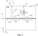
- FIG. 1 schematically illustrates a portion of a photonic chip 100 of a segmented EOM 10 according to an example embodiment.
- the illustrated portion includes an optical waveguide 110, and two RF TLs 121 and 131, all being disposed along a main face 105 of the photonic chip 100.
- the RF TLs 121 and 131 include modulating segments 122 and 132, respectively, which extend along corresponding segments of the optical waveguide 110 and electro-optically cooperate therewith to form two optical modulator segments (OMSs) 120, 130 connected optically in series.
- the second of the two RF TLs, RF TL 131 includes an RF delay line segment 135 upstream of the modulating segment 132 thereof.
- the RF TLs 121 and 131 each typically include at least one signal electrode, which extends along a corresponding segment of the optical waveguide, and at least one ground electrode extending along the signal electrode with the optical waveguide therebetween.
- input light 11 propagating in the optical waveguide 110 passes the modulator segments 120 and 130 sequentially, reaching the second modulator segment 130 with a time delay ⁇ relative to the first modulator segment 120.
- the time delay ⁇ may be referred to as the optical time delay.
- the RF TLs 121 and 131 deliver RF driving signals 12 and 13 to the modulator segments 120, 130 to modulate the light as the light propagates through the corresponding modulator segments.
- the RF driving signals 12 and 13 carry a same data signal, and the RF delay line segment 135 is preferably configured so that the light propagation through the modulator segments 120, 130 is about time-synchronized with the delivery of corresponding portions of the RF driving signals 12, 13 to the respective modulator segments.
- the RF delay line segment 135 may be formed using distributed capacitive loading structures that are vertically capacitively coupled to an adjacent TL segment 133 of the corresponding RF TL 131 so as to slow down the propagation of the RF driving signal 13 relative to a similar segment of the RF TL 131, which does not have or alternatively, has different capacitive loading structure (not shown).
- the length of the capacitively-loaded TL segment 133 and/or the amount of capacitive loading may be configured to provide a desired relative delay, e.g. to match the difference in propagation times of corresponding portions of an RF signal from a common RF driver stage (e.g. 511 in FIGs.
- FIG. 2A illustrates an example modulation segment of an RF TL 230, which may embody either one of the RF TLs 121, 131 schematically shown in FIG. 1 .
- the RF TL 230 is a three-electrode ground-signal-ground (G-S-G) transmission line, with a signal electrode 222 extending between two ground electrodes 221 and 223.
- G-S-G three-electrode ground-signal-ground
- Embodiments in which the second ground electrode 223 is absent, and wherein the RF TL is a two-electrode ground-signal (G-S) TL are also within the scope of the present disclosure.
- the signal electrode 222 extends along a segment 210 of the optical waveguide 110, with a first ground electrode 221 extending therealong on the other side of the optical waveguide 110.
- the signal electrode 222 may also be referred to as the first signal electrode.
- An RF signal propagating in the RF TL 230 modulates a voltage across the optical waveguide 110, changing the optical properties thereof and thereby modulating light propagating in the optical waveguide.
- the second ground electrode 223 may be provided along the other side of the signal electrode 222 for symmetry, and/or for EM shielding.
- the optical waveguide 110 may be formed with a semiconductor material, e.g. silicon, and include a pin junction that may be suitably biased, e.g. to operate in a depletion mode.
- the optical waveguide 110 may be formed with an electro-optic active material, such as but not exclusively LiNbO3.
- FIG. 2B illustrates an example RF delay line segment 235, which may implement the RF delay line segment 135 of FIG. 1 in embodiments with G-S-G TLs.
- the RF delay line segment 235 includes a segment 240 of the RF TL 230 that is vertically capacitively coupled to a distributed metallic structure 250, also shown separately in FIG. 2D .
- the term “vertical” refers to a direction that is perpendicular to a main face of a chip or substrate along which the corresponding RF TL extends.
- the metallic structure 250 is configured to provide a distributed capacitive loading to the TL segment 240.
- the RF delay line segment 235 may be embodied with a vertical layer stack, having the TL segment 240 disposed in a first layer 261 of the stack ( FIG. 2C ).
- the metallic structure 250 includes a plurality of spaced metallic elements 251, which are spread along a length of the signal electrode 222, e.g. in a vertical alignment therewith, and are capacitively coupled to adjacent segments of the signal electrode 222.
- the spaced metallic elements 251 may be disposed in a second layer 262 ( FIG. 2D ) of the stack, which extends along the first layer 261 and is vertically spaced therefrom.
- the metallic structure 250 further includes a plurality of metal connectors 255 electrically connecting each of the spaced metallic elements 251 to at least one of the ground electrodes 221 and 223.
- the spaced metallic elements 251 may be e.g. in the form of metallic strips, i.e. separate segments of a metallic line, which may be sequentially spread along a length of the first signal electrode 222, e.g., aligned therealong, and separated from each other by gaps to be electrically insulated from each other.
- the spaced metallic elements 251 are positioned vertically over or under the signal electrode 222 with an electrical insulator layer therebetween.
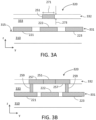
- FIGs. 3A and 3B illustrate an example vertical stack 320 implementing the RF delay line segment 235.
- FIG. 3A shows a first cross-section of the vertical stack, which may represent the cross-section of the RF delay line 235 along a line A-A shown in FIG. 2B .
- FIG. 3B shows a second cross-section of the vertical stack, which may represent the cross-section of the RF delay line 235 along a line B-B shown in FIG. 2B .
- the vertical stack 320 includes, at least, three layers 331, 332, and 333 that are vertically stacked one over the other, with layers 331 and 332 including the first and second metallic layers 261, 262 described above with reference to FIGs. 2C and 2D .
- the vertical stack 320 is disposed over a planar surface 315 of a substrate 310, which may include one or more other layers.
- “vertical” refers to a direction generally perpendicular to the planar surface 315 of the substrate.
- the first layer 331 includes the metallic signal electrode 222 and the metallic ground electrodes 221, 223 of the RF TL 230.
- the second layer 332 includes the metallic elements 251, each being disposed over a corresponding segment of the signal electrode 222 and being capacitively coupled thereto.
- An electrical insulator layer 333 separates the metallic elements 251 from the signal electrode 222.
- the insulator layer 333 may be, for example, a layer of silicon dioxide (SiO2), silicon nitride (Si3N4), or another suitable dielectric, and may have a thickness in a range from 0.05 to 25 microns ( ⁇ m), by way of example.
- EM electromagnetic coupling
- the sequence of metallic elements 251 may be periodically spaced to produce a periodic or nearly-periodic sequence of lumped-element capacitors.
- the metallic elements 251 are spaced aperiodically are also within the scope of the present disclosure.
- the metallic elements 251 may be electrically tied to a ground plane, e.g. electrically connected to at least one of the ground electrodes 221, 223 of the RF TL 230.
- the ground connections are provided by transverse metallic segments 257 and metal filled vias 259, also referred to herein as "ground ties".
- the transverse metallic segments 257 extend in the second layer 332 from the metallic element 251 facing the RF TL, i.e. across the gaps between the signal and ground electrodes thereof, and connect electrically and physically to metal filled vias 259, which pass through the electrical insulator layer 333 and in turn, electrically and physically connect to at least one of the ground electrodes 221 and 223, as illustrated in FIG. 3B for an example embodiment.
- the metallic elements 251 may be made wider or narrower to control the amount of capacitance added to the underlying TL segment 240.
- the sequence of metallic elements 251 is configured so that the metallic structure 250 formed therewith provides distributed capacitive loading to the facing TL segment 240, thereby slowing down RF signals propagating therein.
- the amount of capacitive loading may be adjusted by varying the width 271 of the metallic elements 251.
- the spacing p 263 between the ground ties 259, and/or the length l 281 of each metallic element 251 along the signal electrode 222 may be made sufficiently small relative to a relevant RF wavelength ⁇ m , so that the distributed metallic structure 250 does not substantially affect, or at most weakly affects, the impedance of the RF delay line formed therewith.
- the length l 281 of each metallic element 251 may be less than ⁇ m /4, or even no greater than ⁇ m /10.
- the spacing p 263 between the ground ties may be less than ⁇ m /4, or no greater than ⁇ m /10.
- the frequency f m is related to a baud, or symbol, rate R bd of the optical modulator, and may also depend, e.g., on the data transmission format, and digital processing at the receiver.
- a binary NRZ (non-return-to zero) direct detect modulation format f m may be about 75% of the bit rate of the data signal
- a PAM4 modulation format f m may be about 80% of the baud rate, and about 50% of the baud rate for DPSK.
- the length l 281 of each metallic element 251, and/or the spacing p 263 between the ground ties may be no more than about ⁇ BD /3, or no more than about ⁇ BD /4, or no more than about ⁇ BD /8, wherein ⁇ BD is the wavelength of an RF signal of a frequency f - R bd propagating in the capacitively loaded RF TL segment.
- the relevant RF wavelength ⁇ m depends on the propagation speed of the RF signal in the capacitively loaded (or slow-wave) TL, which can vary by as much as a factor of 5, corresponding to an effective RF propagation constants ranging e.g. from about 2 to about 10.
- ⁇ m may correspond to about 800 ⁇ m, and the element length l, and/or the ground tie spacing p, may be less than about 200 ⁇ m, or no greater than 80 ⁇ m in some embodiments;
- the gaps 288 separating adjacent metallic elements 251 may be, for example, in a range from 1 to 80 ⁇ m.
- the length of the capacitive structure 250 along the RF TL 240 e.g., the length of segment 135 of FIG. 1 , depends on the desired relative delay values between the RF driver signal input to the optical modulation segments 120 and 130 of FIG. 1 .
- the total length of the distributed metallic structure 250 along the signal electrode may be, for example, in a range from about 500 ⁇ m to 10,000 ⁇ m.
- the number of consecutive metallic elements 251 in the distributed metallic structure 250 may be, for example, in a range from 2 to 50 or more.
- the presence of the distributed metallic structure 250 may contribute relatively weakly to the impedance Z ( f ) of the RF delay line segment 235 formed therewith.
- the impedance Z ( f ) of the RF delay line segment 235 can then be controlled somewhat independently via a modification of the delay line inductance and capacitive loading, e.g. by varying the electrode geometry of the underlying RF TL 230, e.g. the width or thickness of the signal electrode 222 and/or its distance from the ground electrodes 221, 223.
- the delay time imparted by the RF delay line segment 235 upon the RF signal propagating therethrough can be changed by modifying its cross-sectional geometry while maintaining the same length of the RF TL.
- the RF propagation constant in the RF delay line 235 can be varied by a factor of about 5, e.g. between values of about 2 and 10 by changing the amount of capacitive loading imparted by the metallic loading structure 250 and the overall inductance of the RF delay line.
- the capacitive loading structures may have a relatively modest impact on the TL inductance, whereas the TL line electrode width and thickness may have a bigger impact on inductance than on capacitance, which may simplify achieving a desired TL design point.
- the propagation speed of RF signals in the RF delay line segment 235 and the impedance of the RF delay line segment 235 may be substantially independently controlled, which may be advantageous for configuring the optical waveguide modulator to a particular environment, e.g. when designed for an environment of 50 Ohms or otherwise.
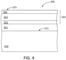
- the vertical stack 320 may be a part of a chip 300, which may include a substrate 310 having a planar surface 315, and a plurality of layers disposed over and along the planar surface 315, including the vertical stack 320.
- the chip 300 may include optical modulator segments embedded therein, such as e.g. the photonic chip 100, with the vertical stack 320 being a part of the photonic chip.
- the chip 300 may also include an optical layer or layers 321, which may include one or more optical waveguides, such as the optical waveguide 110. It will be appreciated that chip 300 may include other layers not shown in FIG. 4 , e.g. below or above the layer or layers 321 and above the vertical stack 320.
- the chip 300 may be a silicon-on-insulator (SOI) chip, with the layer 321 being a silicon layer that may comprise an optical core of the optical waveguide 110, with the substrate 310 including a buried oxide layer adjacent the planar surface 315 thereof.
- the RF delay lines 135, 235 may be fabricated on the photonic chip within the so-called "back end of line” (BEOL) metal layers.
- the vertical stack 320 may be a part of another chip or carrier, such as e.g. an RF driver chip or an RF connector substrate or carrier as described below, with the RF TL 230 connected to drive a modulator segment defined in a photonic chip, e.g. the modulator segment 130 of the photonic chip 100 illustrated in FIG. 1 .
- FIGs. 5A and 5B illustrate example placements of RF delay lines according to the present disclosure in an example segmented optical modulator apparatus 500.
- the apparatus 500 includes an RF driver circuit 505 having three parallel RF outputs 515 connected to drive three optical modulator segments (OMSs) 551 1 , 551 2 , and 551 3 of a segmented Mach-Zehnder modulator (MZM) 550, which are optically connected in series.
- the OMS 551 1 - 551 3 may be generally referred to as OMSs 551i.
- the RF driver circuit 505 may include a common input stage 511 that in operation receives an input RF signal 501 for modulating input light 101 therewith.
- the input stage 511 is connected to drive three parallel output RF drivers 513 1 - 513 3 , one for each OMS 551 i .
- the number N of the OMSs 551 i in the segmented MZM 550, and the corresponding number of the output RF drivers 513 i may range from at least 2 to as many as 10 or greater.
- the output RF drivers 513 1 - 513 3 which may be generally referred to as RF drivers 513 i , may generate amplified portions or copies of the input RF signal 501, which are then individually delivered to respective OMSs 551 i of the segmented MZM 550 over three RF TLs 521 1 - 521 3 ("RF TLs 521 i ").
- Each of the RF TLs 521 i includes an electro-optic modulating TL segment, schematically indicated in FIGs.5A and 5B at 524 1 , 524 2 , and 524 3 , respectively ("modulating TL segments 524 i "), which extend along adjacent segments of the optical waveguide arms 531 and 532 for modulating optical properties thereof with suitably delayed and amplified portions or copies of the input RF signal 501, e.g. the effective refractive index of the segments of the optical waveguide arms 531, 532 within corresponding ones of the OMSs 551 i , which may be conventional OSMs.
- modulating TL segments 524 i which extend along adjacent segments of the optical waveguide arms 531 and 532 for modulating optical properties thereof with suitably delayed and amplified portions or copies of the input RF signal 501, e.g. the effective refractive index of the segments of the optical waveguide arms 531, 532 within corresponding ones of the OMSs 551 i , which may be conventional O
- the second RF TL 521 2 and the third RF TL 521 3 which are connected to drive the second and third OMSs 551 2 and 551 3 , respectively, include corresponding RF delay line segments 535 1 and 535 2 .
- the RF delay line segments 535 1 and 535 2 include vertical capacitive loading of the corresponding RF TL in a vertical layer stack, as described above. The amount of capacitive loading is configured to synchronize the delivery of the amplified portions of the input RF driver signals at the respective second and third OMSs with the arrival of the same part of the input light 101 thereat.
- the RF driver circuit 505 may be implemented as an electrical integrated circuit (IC) in an IC driver chip 510, e.g. using CMOS or SiGe (Silicon Germanium) technology, with the segmented MZM 550 implemented as a photonic integrated circuit (PIC) in a photonic chip 530, e.g. a SiP chip.
- the RF TLs 521 i may be disposed in part in a carrier 520 that is external to the photonic chip 530, and connect to corresponding parts of the RF TLs 521 i on the photonic chip 530 using suitable TL connectors 541.
- the carrier 520 also referred to as the connector substrate 520, may be flip-chip mounted to the photonic chip 530.
- the connector substrate 520 may be, for example, a part of a modulator package, or a separate chip, or any medium suitable for delivering highfrequency RF signals, including but not limited to ceramics and medium built e.g. using organic High Density Build Up (HDBU) technology.
- the IC driver chip 510 may be the carrier that connects to the photonic chip 530 directly using the TL connectors 541, e.g. being flip-chip mounted thereto, in the absence of a connector chip or substrate therebetween.
- one or both of the RF delay lines 531 i may be located in the photonic chip 530, in the RF chip 510, in the connector substrate 520, or in parts in some combination thereof.
- FIG. 5A schematically illustrates an example embodiment where the RF delay lines 531 1 and 531 2 are formed in the photonic chip 530, by capacitively loading segments of the RF TLs 521 1 and 521 2 located in the photonic chip 530, with inter-chip TL connectors 541 located upstream thereof.
- FIG. 5A schematically illustrates an example embodiment where the RF delay lines 531 1 and 531 2 are formed in the photonic chip 530, by capacitively loading segments of the RF TLs 521 1 and 521 2 located in the photonic chip 530, with inter-chip TL connectors 541 located upstream thereof.
- FIG. 5B schematically illustrates another example embodiment where the RF delay lines 531 1 and 531 2 are formed in the connector substrate 520, by capacitively loading segments of the RF TLs 521 1 and 521 2 located in the connector substrate 520, with inter-chip TL connectors 541 located downstream thereof.
- upstream and downstream relate to the direction of propagation of the RF signal 501, or corresponding copies or portions thereof, with the output RF drivers 513i of the RF driver circuit 505 being upstream of the respective OMSs 551 i .
- FIG. 6 illustrates an example segmented MZM 600, which may be an embodiment of the segmented MZM 550, and which includes three OMSs 641 1 , 641 2 , and 641 3 connected optically in series and separately driven by respective modulating TL segments of corresponding RF TLs 621 1 , 621 2 , and 621 3 .
- each of the RF TLs 621 1 , 621 2 , and 621 3 is a G-S-G TL having a signal ("S") electrode 612 between two ground (“G”) electrodes 611 and 613.
- the optical waveguide arms 631 and 632 of the segmented MZM 600 which extend along a main face 615 of a photonic chip and traverse the three OMSs 641 i , are connected optically in parallel, and in operation are driven in a push-pull manner by the RF signals provided over the signal electrodes 612 of the corresponding RF TLs.
- the second RF TL 621 2 includes a first RF delay line segment 635 1
- the third RF TL 621 3 includes a second RF delay line segment 635 2 , each of which may be an embodiment of the RF delay line segment 235 and implemented in a vertical layer stack such as stack 320 described above.
- the first RF delay line segment 635 1 includes a distributed metallic structure 625 1 disposed in parts over and along a segment of the RF TL 621 2 , to provide a distributed capacitive loading thereto.
- the first metallic capacitive loading structure 625 1 includes a sequence of first metallic elements 651 1 aligned over and along adjacent segments of the signal electrode 612 of the RF TL 621 2 in a different layer therefrom, the first metallic elements 651 1 being electrically tied to at least one of the ground electrodes 611, 613 of the TL 621 2 and capacitively coupled to the signal electrode 612 thereof, generally as described above with reference to FIGs. 2B -3C.
- the second RF delay line segment 635 2 includes a second distributed metallic structure 625 2 to provide a distributed capacitive loading to the underlying TL segment of the third TL 621 3 .
- the second metallic capacitive loading structure 625 2 includes a sequence of second metallic elements 651 2 aligned over and along adjacent segments of the signal electrode 612 of the third RF TL 621 3 in a different layer therefrom, the second metallic elements 651 2 being electrically tied to at least one of the ground electrodes of the third TL and capacitively coupled to the signal electrode thereof, also generally as described above with reference to FIGs. 2B -3C.
- the second RF delay line segment 635 2 may be configured to provide a different, e.g.
- the different, e.g. greater, time delay is provided by the second RF delay line segment 635 2 having a different, e.g. greater length.
- the different, e.g. greater, time delay of the second RF delay line segment 635 2 is provided by the second metallic elements 651 2 having a different, e.g. greater width than the first metallic elements 651 1 , and therefore providing a greater capacitive loading to the underlying TL.
- the first and second RF delay lines 635 1 and 625 2 may have about a same length along the signal electrodes of the respective TLs.
- the capacitively-loaded segments of the signal electrodes 732 in the respective RF delay line segments 635 1 and 625 2 may also have different widths to appropriately modify the TL inductance such that a similar line impedance is achieved while realizing a different RF propagation velocity.
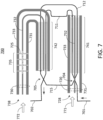
- FIG. 7 illustrates another segmented optical modulator 700, which may include one or more RF delay lines according to embodiments of the present disclosure.
- the segmented optical modulator 700 which may be referred to as a coupling-modulated optical resonator, includes a looped MZM formed with two optical waveguide 711, 712 connected in parallel between an input 2x2 optical coupler 704 and an output 2x2 optical coupler 705.
- One of the remaining two optical ports of the input optical coupler 704 connects to an input optical port 701 of the modulator 700, while one of the remaining two optical ports of the output optical coupler 704 connects to the output optical port 702 of the modulator 700.
- the remaining optical port of the input 2x2 coupler 705 is optically connected to the remaining optical port of the output 2x2 coupler 706, forming a ring optical resonator.
- Two RF TLs 730 and 720 are provided, with input ends thereof for connecting to respective RF outputs of an RF driver circuit, such as the RF outputs 515 of the RF driver circuit 505 of FIGs. 5A or 5B .
- the RF TLs 730 and 720 each include a modulating TL segment located along corresponding adjacently extending segments of the optical waveguides 711 and 712, so as to form two OMSs 741 and 742.
- the first OMSs 741 and the second OMS 742 are connected optically in series and are each configured for push-pull modulation of the optical phase of light portions propagating in the optical waveguides 711 and 712, by the RF signal 771 and 772 provided to the input ends of respective RF TLs.
- the RF TLs 720, 730 each has a G-S-G electrode structure, with a signal electrode 732 disposed between two ground electrodes 731 and 733.
- the second RF TL 730 is disposed to drive the second OMS 742 that is optically downstream of the first OMS 741, and incorporates an RF delay line segment 735.
- the RF delay line segment 735 may be an embodiment of the RF delay lines or delay line segments described above, and may include a distributed metallic structure 725 including a sequence of spaced metallic elements that are electrically tied to the ground, are disposed along adjacent segments of the signal electrode 732 in a different vertical layer therefrom, and configured to be capacitively coupled to the respective adjacent segments of the signal electrode 732, so as to provide a desired amount of capacitive loading to the adjacent, e.g. underlying, segment of the RF TL 730.
- Example embodiments of segmented travelling wave and resonant optical waveguide modulators described above with reference to FIGs. 2A - 7 employed RF TLs having a G-S-G electrode structure, with an optical waveguide disposed between a ground electrode and a signal electrode, and/or a signal electrode disposed between parallel segments of two optical waveguides for push-pull modulation of the effective refractive indices thereof.
- segmented optical waveguide modulators e.g. of the types described above, may include differentially driven OMSs and utilize RF TLs having two signal electrodes for transmitting differential RF signals.
- travelling wave and resonant segmented optical modulators that include an MZM may use two different RF TLs, for example two G-S-G TLs as illustrated in FIGs. 2A-2C , to separately drive parallel segments of the optical waveguide arms of an MZM, e.g. with single-ended components of a differential RF drive signal, to achieve the push-pull modulation with a lower peak-to-peak voltage swing.
- each waveguide arm of an MZM may be differentially driven by an RF TL having two signal electrodes sandwiching a segment of the optical waveguide arm.
- each of the two RF TLs may include a vertically capacitively loaded TL segment forming an RF delay line segment, each of which may be configured generally as described above using suitably adapted distributed metallic structures that are vertically capacitively coupled to adjacent segments of the one or more signal electrodes.
- FIG. 8A schematically illustrates an example OMS 820A that includes segments of two optical waveguides 801 and 802 extending in parallel along and between two signal electrodes 821, 822 of a RF TL 800, which may also include two ground electrodes 810 extending along opposite sides of the signal electrodes 821, 822 ("G-S-S-G TL").
- Each of the segments of the optical waveguides 801, 802 between the signal electrodes 821, 822 may have an optical property, e.g. an effective refractive index of the waveguide, that is electrically controlled by RF signals propagating along the signal electrodes 821 and 822.
- each of the optical waveguides 801 and 802 may be a silicon waveguide having a pin junction in the segment thereof within the OMS 820A, with the two signal electrodes 821, 822 being in electrical contact with the p-doped or n-doped regions of the corresponding pin junctions, to electrically push-pull modulate the free carrier concentration in the waveguide segments therebetween.
- the optical waveguides 801, 802 may be made with an electro-optical material, such as but not exclusively Lithium Niobate (LiNbO3).
- the optical waveguides 801 and 802 may be, for example, two optical arms of an MZM, and the segments thereof between the signal electrodes 821, 822 may be push-pull driven by a differential RF signal propagating along the RF TL 800.
- the RF TL 800 may include a third ground electrode between the signal electrodes 821 and 822.
- FIG. 8B schematically illustrates an example OMS 820B, which may be a variation of OMS 800B wherein the G-S-S-G RF TL 800 is used to individually drive a segment of the optical waveguide 801.
- the optical waveguide 801 may be made with an electro-optical material, such as but not exclusively Lithium Niobate (LiNbO3).
- the optical waveguide 801 may be, for example, one optical waveguide arm of an MZM, and the segment thereof between the signal electrodes 821, 822 may be driven by a differential RF signal propagating along the RF TL 800, with the other optical waveguide arm of the MZM driven by another G-S-S-G TL.
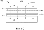
- FIG. 8C illustrates an example RF delay line segment 835 that may be formed with a segment of the G-S-S-G TL 800 electrically upstream of the OMS 820A or OMS 820B.
- the RF delay line segment 835 includes a distributed metallic structure 825 having two sets of spaced metallic elements, 851 and 852, disposed in a different layer than the TL, sequentially aligned along respective signal electrodes 821 and 822, and electrically tied to at least one of the ground electrodes 810, e.g. generally as described above with reference to FIGs. 2A-3B and the spaced metallic elements 251.
- FIGs. 9 and 10 schematically illustrate, in a cross-sectional view, two such example embodiments where a photonic chip 900 comprising a segmented optical modulator PIC (not shown) is flip-chip bonded to a carrier 970, e.g. a second chip or substrate, e.g. an RF driver chip or an RF connector chip or substrate, such as the RF driver chip 510 or the connector substrate 520 described above with reference to FIGs. 5A and 5B .
- a carrier 970 e.g. a second chip or substrate, e.g. an RF driver chip or an RF connector chip or substrate, such as the RF driver chip 510 or the connector substrate 520 described above with reference to FIGs. 5A and 5B .
- the photonic chip 900 includes, at least, a substrate 910 having a planar surface 915, one or more optical layers 921 disposed along the planar surface 915 and including an optical waveguide (not shown), and an RF TL 940 having a segment (not shown) extending along a segment of an optical waveguide and electro-optically coupled thereto to form an OMS (not shown), e.g. as described above with reference to FIGs. 1 , 2A , and 5A-8A .
- the second chip or substrate 970 has a main face 971 facing the main face of the photonic chip 900 with a small gap therebetween, and includes RF TLs 972 that extend along the main face 971 of the second chip 970.
- Each RF TL 972 connects to the corresponding RF TL 940 of the photonic chip using a suitable inter-chip TL connector, which may include, e.g. one or more solder bumps.
- the RF TLs 940 and 972 include each at least one signal electrode and at least one ground electrode extending therealong (not shown), and may have a same G-S, G-S-G, or G-S-S-G electrode structure, among others.
- the RF TLs 972 and 940 may be viewed as different segments of a same RF TL extending across two or more different chips and/or substrates.
- Both embodiments further include a vertical layer stack 930 comprising RF delay line segment(s) 935 electrically connected to the corresponding OMSes (not shown) via the RF TLs 940 and 972.
- Each RF delay line segment 935 may be an embodiment of the RF delay lines or RF delay line segments described above, with the spaced metallic elements 951 vertically capacitively coupled to a signal electrode segment of a corresponding RF TL and embodying the corresponding spaced metallic elements of the RF delay lines described above.
- the vertical layer stack 930 is disposed in the photonic chip 900 along a main face 925 thereof, and includes the RF TLs 940, or at least segments thereof, in a first layer 931 of the stack and sequences of spaced metallic elements 951 in a second layer 932 of the stack, which is separated from the first layer by an intermediate non-metallic electrical insulator layer 933.
- the spaced metallic elements 951 are capacitively coupled to underlying segments of the signal electrodes 941 of the RF TLs 940, to form the RF delay line segments 935, and may be electrically tied, i.e. DC coupled, to the ground electrode(s) as described above.
- the spaced metallic elements 951 may be formed, e.g. within the back end of line (BEOL) metal layers of the photonic chip.
- the vertical layer stack 930 is in the second chip or carrier 970 along a main face 971 thereof, and includes the RF TLs 972, or at least segments thereof, in the first layer 931, and the sequences of spaced metallic elements 951 in the second, separate layer 932 of the stack.
- the spaced metallic elements 951 are capacitively coupled to underlying segments of the signal electrodes 977 of the RF TLs 972 to form lumped-element capacitors therewith, which may be e.g. periodically spaced along the TLs, to provide the RF delay line segments 935.
- the spaced metallic elements 951 may be electrically tied to the ground electrode(s) of the RF TL 972, as described above.
- the spaced metallic elements 951 and portions of the ground connectors associated therewith are disposed closer to the main face of the corresponding chip than the signal electrode segment of the RF TL to which they are capacitively coupled; they may be fabricated, e.g. in a higher BEOL layer than the TL electrodes.
- the spaced metallic elements 951 may be in the first layer 931 of the vertical stack 930, with the signal electrode 941 of the TL 940 or 972 positioned in the second layer 932 that is closer to the main face 925 of the photonic chip 900 and/or the main face 971 of the second chip 970.
- the capacitive loading structures may at least partially shield the underlying segment of the RF TLs 940 or 972 from possible environmental influences from above the main face of the corresponding chip 900 or 970.
- the gap between the chips 900 and 970 above the RF delay line segment 935 is non-uniformly filled with an underfill material 960, the RF propagation speed along the RF delay line segment, and the overall RF delay it provides, may be impacted by packaging variations, e.g., variable underfill placement near an edge of the photonic chip.
- packaging variations e.g., variable underfill placement near an edge of the photonic chip.
- Having the metallic capacitive loading structures in a higher metal layer than the RF electrodes, i.e. between the RF TL electrodes and the main face of the chip may result in a device design that is more robust to packaging variations.
- segmented optical modulators and RF delay lines connected thereto are not intended to be limiting, and many variations will become apparent to a skilled reader having the benefit of the present disclosure.
- the concrete shape of the spaced metallic elements 251, 651, 851, 951 that provide the desired capacitive loading to the underlying signal electrode(s) of a TL may vary, and may generally differ from a rectangular stripe.
- their connections 257, 259 to the ground electrode(s) may be differently arranged, for example using offset transverse metallic segments as illustrated in FIG. 11 .
- embodiments may be envisioned where some of metal element 251, 651, 851, 852 are electrically tied to only one ground electrode of the corresponding RF TL.
- multi-segment EOMs such as those described above may be implemented in material systems other than those based on silicon, and may use electro-optical effects other than those based on free carrier injection or depletion.
- materials and material systems that may be used to implement one or more modulator segments of an EOM include photonic-crystals, integrated graphene layers, various compound semiconductor materials such as those of the III-V group, or thin-film LiNbO3 integrated on a suitable, e.g. silicon, substrate.
Landscapes
- Physics & Mathematics (AREA)
- Nonlinear Science (AREA)
- General Physics & Mathematics (AREA)
- Optics & Photonics (AREA)
- Electromagnetism (AREA)
- Chemical & Material Sciences (AREA)
- Engineering & Computer Science (AREA)
- Ceramic Engineering (AREA)
- Crystallography & Structural Chemistry (AREA)
- Optical Modulation, Optical Deflection, Nonlinear Optics, Optical Demodulation, Optical Logic Elements (AREA)
Abstract
Description
- The present invention generally relates to optical modulators, and more particularly relates to an optical waveguide modulator with segmented electrodes.
- Broad-band optical communications typically require high-speed electro-optical modulators (EOM) to modulate light at a desired data rate. One common type of a broad-band EOM is a Mach-Zehnder modulator (MZM), which uses an optical waveguide structure forming an Mach-Zehnder interferometer (MZI), with RF-driven optical phase modulators in each waveguide arm. The optical waveguide arms of the MZM are typically formed in a suitable semiconductor or other electro-optic material such as LiNbO3, so that light propagation in the waveguide arms may be controlled by applying a voltage there across. Such an optical waveguide modulator may be implemented in an opto-electronic chip as a photonic integrated circuit (PIC).
- A silicon photonics (SiP) platform, e.g., based on a Silicon-on-Insulator (SOI) technology, may be particularly attractive for implementing broad-band EOMs, which can, e.g., enable a natural integration with CMOS-based high-speed electronic drivers. In the SiP platform, voltage-controlled optical phase modulators may be formed by incorporating pin junctions into optical waveguides, such as an optical waveguide arm of an MZM. An electrode extending along a length of the optical waveguide arm in an electrical contact with the pin junction may be used to either inject electrical charge carriers (forward bias) or deplete carriers (reverse bias) in the optical waveguide core, thereby modulating the effective refractive index of the optical waveguide, and the phase of light propagating therethrough.
- At modulation rates in the range of tens of gigabits per second (Gb/s) and higher, electrical transmission lines formed with properly terminated travelling-wave (TW) electrodes are typically used to carry RF electrical drive signals for controlling optical phase modulators in such optical waveguides. However, the RF signal loss in the electrical transmission line, velocity mismatch between the optical and electrical waves, as well as increasing optical loss, limit the total optical phase shift that may be achieved by increasing the modulator length. Some optical modulators have a series of optical modulator segments.
- In various embodiments, an optical modulator has a series of optically connected optical modulator segments, and each such optical modulator segment is driven by a separate RF driver output stage or an electronic driver. The series of optical modulator segments can be operated to produce a total phase shift proportional to the length of the series if the electrical RF driver signals from the separate RF driver outputs and the optical signal are approximately temporally synchronized in individual ones of the optical modulator segments. Herein, some embodiments may provide such approximate synchronization by relatively delaying different ones of the electrical RF driver signals via propagation through corresponding RF transmission lines of a parallel array thereof.
- Some embodiments may implement a bandwidth/drive-voltage tradeoff in a TW EOM by incorporating multiple TW modulation segments along an individual optical waveguide of a EOM device. By combining the modulation response of multiple TW modulation segments in a cumulative way, e.g., a relatively low drive voltage can be used.
- An aspect of the present disclosure relates to an apparatus comprising a photonic chip having a planar main face and comprising a segmented optical modulator having a plurality of optical waveguide modulation segments, the optical waveguide modulation segments being located along the main face and being optically connected in series. The apparatus further comprises a vertical stack, at least, including: a first layer comprising a plurality of metallic radio frequency (RF) transmission lines therein, each metallic RF transmission line being electrically connected to drive a corresponding one of the optical waveguide modulation segments, and a second layer extending along and separate from the first layer and comprising separate metallic structures therein, the metallic structures being capacitively coupled to adjacent segments of one or more of the metallic RF transmission lines; and an electrical insulating layer located between the first and second layers.
- In some implementations, each of the metallic RF transmission lines may comprise a signal electrode and at least one ground electrode; wherein some of the metallic structures face one of the RF transmission lines and are capacitively coupled to an adjacent segment of the signal electrode thereof and connected by metallic connectors to the at least one ground electrode thereof. In any of such implementations, the some of the metallic structures capacitively coupled to an adjacent segment of the signal electrode may comprise first metallic segments aligned along the segment of the signal electrode. In any of the implementations including the metallic connectors, the metallic connectors may each comprise a metallic segment extending transverse to the adjacent segment of the signal electrode and be physically connected by a metal portion traversing the electrical insulating layer to the at least one ground electrode of the one of the RF transmission lines.
- In any of the above implementations, the metallic structures may have linear dimensions less than or equal to one quarter of a wavelength of an RF signal propagating along one of the RF transmission lines with a frequency of a baud rate of the RF driver circuit.
- In any of the above implementations, the metallic structures may have a length along the adjacent segment of the signal electrode that is smaller than one quarter of a wavelength of an RF signal propagating along one of the RF transmission lines and having a frequency of a baud rate of the RF driver circuit.
- In any of the above implementations wherein the RF transmission lines each comprise a signal electrode, some of the metallic structures may have segments of a first width along the adjacent segment of the signal electrode of the one of the RF transmission lines and others of the metallic structures have segments of a different second width along an adjacent segment of a signal electrode of another of the RF transmission lines.
- In any of the above implementations, the second layer may be between the main face and the first layer.
- In any of the above implementations, the vertical stack may be in the photonic chip, or flip-chip mounted to the photonic chip, or in a carrier external to the photonic chip. In some implementations, the carrier may be flip-chip mounted to the photonic chip.
- In any of the above implementations, the photonic chip may comprise an optical waveguide extending along the main face, and the RF transmission lines may comprise segments extending adjacent and along corresponding segments of the optical waveguide to form the optical waveguide modulator segments therewith. In some implementations, the optical waveguide may be an optical waveguide arm of a Mach-Zehnder modulator located along the main face.
- In any of the above implementations, the optical modulator may comprise an optical resonator including a segmented Mach-Zehnder modulator comprising the optical waveguide modulation segments.
- In any of the above implementations, at least one of the RF transmission lines may comprise two ground electrodes and two signal electrodes extending between the two ground electrodes, wherein some of the metallic structures form sequences along adjacent segments of the signal electrodes and are electrically connected by metal connectors to at least one of the ground electrodes.
- Any of the above implementations may include an RF driver circuit having an array of parallel RF outputs, each of the RF outputs being electrically connected to a corresponding one of the metallic RF transmission lines. A first of the metallic RF transmission lines may be, in at least some implementations, configured to cause a first delay for an RF signal to propagate therethrough and a second of the metallic RF transmission lines may be configured to cause a different delay for an RF signal to propagate therethrough.
- A related aspect of the present disclosure provides a segmented optical modulator comprising: a photonic chip having a planar main face and comprising an optical waveguide modulator including two optical modulator segments located along the main face and optically connected in series; first and second radio frequency (RF) transmission lines therein, each comprising at least one signal electrode and being connected to drive a corresponding one of the two optical modulator segments; and a vertical stack, the vertical stack at least, comprising: a first layer comprising at least a segment of the at least one signal electrode of the second RF transmission line; a second layer extending along the first layer and comprising a metallic structure adjacent to the at least a segment of the at least one signal electrode and capacitively coupled thereto; and an insulating layer located between the first and second layers.
- A related aspect of the present disclosure provides a segmented optical modulator comprising: a photonic chip having a planar main face and comprising an optical modulator including two optical waveguide modulation segments located along the main face and optically connected in series; first and second radio frequency (RF) transmission lines, each of the transmission lines comprising a signal electrode and being connected to drive a corresponding one of the two optical waveguide modulation segments; and a plurality of spaced apart and ground-connected metallic elements being disposed in sequence along a segment of the second RF transmission line, being capacitively coupled thereto and being at a different vertical distance from the planar main face than the second RF transmission line.
- Embodiments disclosed herein will be described in greater detail with reference to the accompanying drawings which represent example embodiments thereof, which are not to scale, in which like elements are indicated with like reference numerals, and wherein:
-
FIG. 1 is a schematic top view of a portion of a photonic chip with a segmented optical waveguide modulator having an on-chip RF delay line formed using distributed capacitive loading of a segment of an RF transmission line (TL); -
FIG. 2A is a schematic top view of a modulating segment of an example G-S-G RF TL of a segmented optical waveguide modulator according to an embodiment; -
FIG. 2B is a schematic top view of an RF delay line formed with a capacitively-loaded segment of the RF TL ofFIG. 2A according to an embodiment; -
FIG. 2C is a schematic top view of the TL segment ofFIG. 2B in a first layer of a vertical layer stack; -
FIG. 2D is a schematic top view of the distributed metallic structure in a second layer of the vertical layer stack above or below the TL segment ofFIG. 2C ; -
FIG. 3A is a schematic first partial cross-section of the example RF delay line ofFIG. 2B along the A-A line; -
FIG. 3B is a schematic second partial cross-section of the example RF delay line ofFIG. 2B along the B-B line; -
FIG. 4 is a schematic partial cross-section of a photonic chip including a vertical layer stack of an RF delay line according to an embodiment; -
FIG. 5A is a schematic functional diagram of an example segmented optical modulator apparatus having RF delay lines with vertically-loaded TL segments located in a photonic chip; -
FIG. 5B is a schematic functional diagram of an example segmented optical modulator apparatus having RF delay lines with vertically-loaded TL segments in a carrier connected to the photonic chip; -
FIG. 6 is a schematic diagram illustrating a parallel array of vertically-loaded segments of RF TLs driving a TW Mach-Zehnder modulator (MZM); -
FIG. 7 is a schematic diagram illustrating a vertically-loaded segment of an RF TL driving a segment of a coupling modulated resonator; -
FIG. 8A is a schematic top view of a G-S-S-G RF TL disposed to drive parallel segments of two optical waveguide arms of a segmented optical waveguide modulator; -
FIG. 8B is a schematic top view of a G-S-S-G RF TL disposed to drive a segment of an optical waveguide of a segmented optical waveguide modulator; -
FIG. 8C is a schematic top view of a vertically-loaded RF delay segment of the G-S-S-G RF TL ofFIG. 8A according to an embodiment; -
FIG. 9 is a schematic cross-sectional view of a photonic chip flip-chip mounted to a carrier, with RF delay lines based on a vertically-loaded TLs in the photonic chip; -
FIG. 10 is a schematic cross-sectional view of a photonic chip flip-chip mounted to a carrier, with RF delay lines based on a vertically-loaded TLs in the carrier; -
FIG. 11 is a schematic diagram illustrating an example capacitive loading element with offset ground connectors. - In the following description, for purposes of explanation and not limitation, specific details are set forth, such as particular circuits, circuit components, techniques, etc. in order to provide a thorough understanding of the present invention. However, it will be apparent to one skilled in the art that the present invention may be practiced in other embodiments that depart from these specific details. In other instances, detailed descriptions of well-known methods, devices, and circuits are omitted so as not to obscure the description of the present invention. All statements herein reciting principles, aspects, and embodiments of the invention, as well as specific examples thereof, are intended to encompass both structural and functional equivalents thereof. Additionally, it is intended that such equivalents include both currently known equivalents as well as equivalents developed in the future.
- Furthermore, the following abbreviations and acronyms may be used in the present document:
- "CMOS" Complementary Metal-Oxide-Semiconductor
- "GaAs" Gallium Arsenide
- "InP" Indium Phosphide
- "Si" Silicon
- "SiO2" Silicon Dioxide
- "LiNbO3" Lithium Niobate
- "PIC" Photonic Integrated Circuit
- "SOI" Silicon on Insulator
- "SiP" Silicon Photonics
- "RF" Radio Frequency
- "DC" Direct Current
- "AC" Alternate Current
- "TW" Travelling Wave
- "G-S-G" Ground-Signal-Ground
- "G-S-S-G" Ground-Signal-Signal-Ground
- Note that as used herein, the terms "first", "second" and so forth are not intended to imply sequential ordering, but rather are intended to distinguish one element from another, unless explicitly stated. Similarly, sequential ordering of method steps does not imply a requirement of sequential order of their execution, unless explicitly stated. The term "connected" may encompass direct connections or indirect connections through intermediate elements, unless explicitly stated otherwise. The term "electrically connected" and its derivatives refers to DC connections unless explicitly stated otherwise. Herein, the term pin junction encompasses both strict pin junctions having only contacting p-doped and n-doped regions and p/i/n junctions having a region of substantially intrinsic conductivity located between the p-doped and n-doped regions. The term "differential signal" refers to a signal that is transmitted using two single-ended signals having about complementary AC components. The term "substrate" encompasses single and multi-layer structures. The term "RF" (Radio Frequency) refers to frequencies in a range from megahertz (MHz) to about one terahertz (THz). The term "high-speed RF signals" refer to RF signals at frequencies above 10 gigahertz (GHz).
- A traveling wave (TW) electrode supports propagation of an RF operating signal there along. Typical TW electrodes usually are longer than about 1/10th of a smallest operating wavelength for an RF signal propagating along the electrode. TW electrodes are often electrically terminated to, at least, partially suppress back reflections of the RF signal at their ends, or even to totally suppress such back reflections. For example, such an electrical termination may be a matched electrical connection to a chip ground or a DC source.
- The present disclosure describes examples of segmented electro-optic modulators (EOMs) using travelling-wave RF transmission lines (TLs) to individually drive different optical modulator segments (OMSs) of the segmented EOMs, with RF TLs having vertically-loaded TL segments to implement one or more RF delay lines, said vertically loaded TL segments being vertically capacitively coupled to distributed metallic loading structures.
-
FIG. 1 schematically illustrates a portion of aphotonic chip 100 of asegmented EOM 10 according to an example embodiment. The illustrated portion includes anoptical waveguide 110, and twoRF TLs main face 105 of thephotonic chip 100. TheRF TLs segments optical waveguide 110 and electro-optically cooperate therewith to form two optical modulator segments (OMSs) 120, 130 connected optically in series. The second of the two RF TLs,RF TL 131, includes an RFdelay line segment 135 upstream of the modulatingsegment 132 thereof. TheRF TLs - In operation, input light 11 propagating in the
optical waveguide 110 passes themodulator segments second modulator segment 130 with a time delay τ relative to thefirst modulator segment 120. The time delay τ may be referred to as the optical time delay. TheRF TLs modulator segments delay line segment 135 is preferably configured so that the light propagation through themodulator segments - The RF
delay line segment 135 may be formed using distributed capacitive loading structures that are vertically capacitively coupled to anadjacent TL segment 133 of the correspondingRF TL 131 so as to slow down the propagation of theRF driving signal 13 relative to a similar segment of theRF TL 131, which does not have or alternatively, has different capacitive loading structure (not shown). The length of the capacitively-loadedTL segment 133 and/or the amount of capacitive loading may be configured to provide a desired relative delay, e.g. to match the difference in propagation times of corresponding portions of an RF signal from a common RF driver stage (e.g. 511 inFIGs. 5A and5B ) to RF inputs of themodulator segments first modulator segment 120 to the input end of thesecond modulator segment 130. - Example embodiments of the RF
delay line segment 135 will now be described with reference toFIGs. 2A-2C .FIG. 2A illustrates an example modulation segment of anRF TL 230, which may embody either one of theRF TLs FIG. 1 . In the illustrated embodiment theRF TL 230 is a three-electrode ground-signal-ground (G-S-G) transmission line, with asignal electrode 222 extending between twoground electrodes second ground electrode 223 is absent, and wherein the RF TL is a two-electrode ground-signal (G-S) TL, are also within the scope of the present disclosure. In the modulating TL segment, thesignal electrode 222 extends along asegment 210 of theoptical waveguide 110, with afirst ground electrode 221 extending therealong on the other side of theoptical waveguide 110. Thesignal electrode 222 may also be referred to as the first signal electrode. An RF signal propagating in theRF TL 230 modulates a voltage across theoptical waveguide 110, changing the optical properties thereof and thereby modulating light propagating in the optical waveguide. Thesecond ground electrode 223 may be provided along the other side of thesignal electrode 222 for symmetry, and/or for EM shielding. By way of example, theoptical waveguide 110 may be formed with a semiconductor material, e.g. silicon, and include a pin junction that may be suitably biased, e.g. to operate in a depletion mode. In other embodiments, theoptical waveguide 110 may be formed with an electro-optic active material, such as but not exclusively LiNbO3. -
FIG. 2B illustrates an example RFdelay line segment 235, which may implement the RFdelay line segment 135 ofFIG. 1 in embodiments with G-S-G TLs. The RFdelay line segment 235 includes asegment 240 of theRF TL 230 that is vertically capacitively coupled to a distributedmetallic structure 250, also shown separately inFIG. 2D . Here the term "vertical" refers to a direction that is perpendicular to a main face of a chip or substrate along which the corresponding RF TL extends. Themetallic structure 250 is configured to provide a distributed capacitive loading to theTL segment 240. The RFdelay line segment 235 may be embodied with a vertical layer stack, having theTL segment 240 disposed in afirst layer 261 of the stack (FIG. 2C ). Themetallic structure 250 includes a plurality of spacedmetallic elements 251, which are spread along a length of thesignal electrode 222, e.g. in a vertical alignment therewith, and are capacitively coupled to adjacent segments of thesignal electrode 222. The spacedmetallic elements 251 may be disposed in a second layer 262 (FIG. 2D ) of the stack, which extends along thefirst layer 261 and is vertically spaced therefrom. Themetallic structure 250 further includes a plurality ofmetal connectors 255 electrically connecting each of the spacedmetallic elements 251 to at least one of theground electrodes - The spaced
metallic elements 251 may be e.g. in the form of metallic strips, i.e. separate segments of a metallic line, which may be sequentially spread along a length of thefirst signal electrode 222, e.g., aligned therealong, and separated from each other by gaps to be electrically insulated from each other. In a typical embodiment the spacedmetallic elements 251 are positioned vertically over or under thesignal electrode 222 with an electrical insulator layer therebetween. -
FIGs. 3A and 3B illustrate an examplevertical stack 320 implementing the RFdelay line segment 235.FIG. 3A shows a first cross-section of the vertical stack, which may represent the cross-section of theRF delay line 235 along a line A-A shown inFIG. 2B .FIG. 3B shows a second cross-section of the vertical stack, which may represent the cross-section of theRF delay line 235 along a line B-B shown inFIG. 2B . Thevertical stack 320 includes, at least, threelayers layers metallic layers FIGs. 2C and 2D . Thevertical stack 320 is disposed over aplanar surface 315 of asubstrate 310, which may include one or more other layers. Here, "vertical" refers to a direction generally perpendicular to theplanar surface 315 of the substrate. Thefirst layer 331 includes themetallic signal electrode 222 and themetallic ground electrodes RF TL 230. Thesecond layer 332 includes themetallic elements 251, each being disposed over a corresponding segment of thesignal electrode 222 and being capacitively coupled thereto. Anelectrical insulator layer 333 separates themetallic elements 251 from thesignal electrode 222. In embodiments using a SiP platform, theinsulator layer 333 may be, for example, a layer of silicon dioxide (SiO2), silicon nitride (Si3N4), or another suitable dielectric, and may have a thickness in a range from 0.05 to 25 microns (µm), by way of example. Eachmetallic element 251 and the adjacent segment of thesignal electrode 222 cooperate, by means of electromagnetic coupling (EM), to form a lumped capacitor, with themetallic element 251 being one plate of the lumped capacitor and a facing segment of thesignal electrode 222 functioning as the other plate of the lumped capacitor. In some embodiments, the sequence ofmetallic elements 251 may be periodically spaced to produce a periodic or nearly-periodic sequence of lumped-element capacitors. Embodiments in which themetallic elements 251 are spaced aperiodically are also within the scope of the present disclosure. - The
metallic elements 251 may be electrically tied to a ground plane, e.g. electrically connected to at least one of theground electrodes RF TL 230. In the illustrated embodiment, the ground connections are provided by transversemetallic segments 257 and metal filledvias 259, also referred to herein as "ground ties". The transversemetallic segments 257 extend in thesecond layer 332 from themetallic element 251 facing the RF TL, i.e. across the gaps between the signal and ground electrodes thereof, and connect electrically and physically to metal filledvias 259, which pass through theelectrical insulator layer 333 and in turn, electrically and physically connect to at least one of theground electrodes FIG. 3B for an example embodiment. Themetallic elements 251 may be made wider or narrower to control the amount of capacitance added to theunderlying TL segment 240. - Referring also back to
FIGs. 2B and2D , the sequence ofmetallic elements 251 is configured so that themetallic structure 250 formed therewith provides distributed capacitive loading to the facingTL segment 240, thereby slowing down RF signals propagating therein. For a given overall length of themetallic structure 250 along the RF TL, the amount of capacitive loading may be adjusted by varying thewidth 271 of themetallic elements 251. Thespacing p 263 between the ground ties 259, and/or thelength l 281 of eachmetallic element 251 along thesignal electrode 222 may be made sufficiently small relative to a relevant RF wavelength λm, so that the distributedmetallic structure 250 does not substantially affect, or at most weakly affects, the impedance of the RF delay line formed therewith. By way of example, in some embodiments thelength l 281 of eachmetallic element 251 may be less than λm/4, or even no greater than λm/10. In some embodiments thespacing p 263 between the ground ties may be less than λm/4, or no greater than λm/10. Here, the relevant RF wavelength λm may be the wavelength of an RF signal of a frequency f m propagating in the capacitively loaded RF TL segment, wherein f m is a frequency at an upper edge of a target frequency bandwidth for the data signal being transmitted, e.g. the 3dB frequency bandwidth thereof, f m=f 3Db. The frequency f m is related to a baud, or symbol, rate R bd of the optical modulator, and may also depend, e.g., on the data transmission format, and digital processing at the receiver. By way of example, for a binary NRZ (non-return-to zero) direct detect modulation format f m may be about 75% of the bit rate of the data signal, for a PAM4 modulation format f m may be about 80% of the baud rate, and about 50% of the baud rate for DPSK. Accordingly, in various example embodiments, thelength l 281 of eachmetallic element 251, and/or thespacing p 263 between the ground ties, may be no more than about λBD/3, or no more than about λBD/4, or no more than about λBD/8, wherein λBD is the wavelength of an RF signal of a frequency f - R bd propagating in the capacitively loaded RF TL segment. - The relevant RF wavelength λm depends on the propagation speed of the RF signal in the capacitively loaded (or slow-wave) TL, which can vary by as much as a factor of 5, corresponding to an effective RF propagation constants ranging e.g. from about 2 to about 10. By way of example, for an optical modulator configured for NRZ modulation and implemented in a silicon photonics (SiP) chip with an RF delay line having an RF propagation constant of about 5 to operate at a baud or symbol rate of 100 Gbaud, λm may correspond to about 800 µm, and the element length l, and/or the ground tie spacing p, may be less than about 200 µm, or no greater than 80 µm in some embodiments; for NRZ and PAM4 optical modulators, the above cited example length values scale approximately in proportion to a ratio k = (100/R bd) for other baud rates R bd expressed in Gbaud, and the same RF propagation constant in the delay line segment. The
gaps 288 separating adjacentmetallic elements 251 may be, for example, in a range from 1 to 80 µm. The length of thecapacitive structure 250 along theRF TL 240, e.g., the length ofsegment 135 ofFIG. 1 , depends on the desired relative delay values between the RF driver signal input to theoptical modulation segments FIG. 1 . In some embodiments, the total length of the distributedmetallic structure 250 along the signal electrode may be, for example, in a range from about 500 µm to 10,000 µm. The number of consecutivemetallic elements 251 in the distributedmetallic structure 250 may be, for example, in a range from 2 to 50 or more. - With the suitably short
metallic elements 251, the presence of the distributedmetallic structure 250 may contribute relatively weakly to the impedance Z(f) of the RFdelay line segment 235 formed therewith. The impedance Z(f) of the RFdelay line segment 235 can then be controlled somewhat independently via a modification of the delay line inductance and capacitive loading, e.g. by varying the electrode geometry of theunderlying RF TL 230, e.g. the width or thickness of thesignal electrode 222 and/or its distance from theground electrodes delay line segment 235 upon the RF signal propagating therethrough can be changed by modifying its cross-sectional geometry while maintaining the same length of the RF TL. For example, we estimate that in some embodiments the RF propagation constant in theRF delay line 235 can be varied by a factor of about 5, e.g. between values of about 2 and 10 by changing the amount of capacitive loading imparted by themetallic loading structure 250 and the overall inductance of the RF delay line. We note that the capacitive loading structures may have a relatively modest impact on the TL inductance, whereas the TL line electrode width and thickness may have a bigger impact on inductance than on capacitance, which may simplify achieving a desired TL design point. Accordingly, the propagation speed of RF signals in the RFdelay line segment 235 and the impedance of the RFdelay line segment 235 may be substantially independently controlled, which may be advantageous for configuring the optical waveguide modulator to a particular environment, e.g. when designed for an environment of 50 Ohms or otherwise. - Referring now to
FIG. 4 , thevertical stack 320 may be a part of achip 300, which may include asubstrate 310 having aplanar surface 315, and a plurality of layers disposed over and along theplanar surface 315, including thevertical stack 320. In some implementations, thechip 300 may include optical modulator segments embedded therein, such as e.g. thephotonic chip 100, with thevertical stack 320 being a part of the photonic chip. In such embodiments thechip 300 may also include an optical layer or layers 321, which may include one or more optical waveguides, such as theoptical waveguide 110. It will be appreciated thatchip 300 may include other layers not shown inFIG. 4 , e.g. below or above the layer or layers 321 and above thevertical stack 320. By way of example, thechip 300 may be a silicon-on-insulator (SOI) chip, with thelayer 321 being a silicon layer that may comprise an optical core of theoptical waveguide 110, with thesubstrate 310 including a buried oxide layer adjacent theplanar surface 315 thereof. In example embodiments, theRF delay lines vertical stack 320 may be a part of another chip or carrier, such as e.g. an RF driver chip or an RF connector substrate or carrier as described below, with theRF TL 230 connected to drive a modulator segment defined in a photonic chip, e.g. themodulator segment 130 of thephotonic chip 100 illustrated inFIG. 1 . -
FIGs. 5A and5B illustrate example placements of RF delay lines according to the present disclosure in an example segmentedoptical modulator apparatus 500. Theapparatus 500 includes anRF driver circuit 505 having threeparallel RF outputs 515 connected to drive three optical modulator segments (OMSs) 5511, 5512, and 5513 of a segmented Mach-Zehnder modulator (MZM) 550, which are optically connected in series. The OMS 5511 - 5513 may be generally referred to as OMSs 551i. TheRF driver circuit 505 may include acommon input stage 511 that in operation receives aninput RF signal 501 for modulating input light 101 therewith. Theinput stage 511 is connected to drive three parallel output RF drivers 5131 - 5133, one for each OMS 551i. The number N of the OMSs 551i in thesegmented MZM 550, and the corresponding number of the output RF drivers 513i, may range from at least 2 to as many as 10 or greater. The output RF drivers 5131 - 5133, which may be generally referred to as RF drivers 513i, may generate amplified portions or copies of theinput RF signal 501, which are then individually delivered to respective OMSs 551i of thesegmented MZM 550 over three RF TLs 5211 - 5213 ("RF TLs 521i"). Each of the RF TLs 521i includes an electro-optic modulating TL segment, schematically indicated inFIGs.5A and5B at 5241, 5242, and 5243, respectively ("modulating TL segments 524i"), which extend along adjacent segments of theoptical waveguide arms input RF signal 501, e.g. the effective refractive index of the segments of theoptical waveguide arms - The second RF TL 5212 and the third RF TL 5213, which are connected to drive the second and
third OMSs input light 101 thereat. - In some embodiments, the
RF driver circuit 505 may be implemented as an electrical integrated circuit (IC) in anIC driver chip 510, e.g. using CMOS or SiGe (Silicon Germanium) technology, with thesegmented MZM 550 implemented as a photonic integrated circuit (PIC) in aphotonic chip 530, e.g. a SiP chip. In some embodiments, the RF TLs 521i may be disposed in part in acarrier 520 that is external to thephotonic chip 530, and connect to corresponding parts of the RF TLs 521i on thephotonic chip 530 usingsuitable TL connectors 541. In some embodiments, thecarrier 520, also referred to as theconnector substrate 520, may be flip-chip mounted to thephotonic chip 530. Theconnector substrate 520 may be, for example, a part of a modulator package, or a separate chip, or any medium suitable for delivering highfrequency RF signals, including but not limited to ceramics and medium built e.g. using organic High Density Build Up (HDBU) technology. In some embodiments theIC driver chip 510 may be the carrier that connects to thephotonic chip 530 directly using theTL connectors 541, e.g. being flip-chip mounted thereto, in the absence of a connector chip or substrate therebetween. - In various embodiments, one or both of the RF delay lines 531i may be located in the
photonic chip 530, in theRF chip 510, in theconnector substrate 520, or in parts in some combination thereof.FIG. 5A schematically illustrates an example embodiment where theRF delay lines photonic chip 530, by capacitively loading segments of the RF TLs 5211 and 5212 located in thephotonic chip 530, withinter-chip TL connectors 541 located upstream thereof.FIG. 5B schematically illustrates another example embodiment where theRF delay lines connector substrate 520, by capacitively loading segments of the RF TLs 5211 and 5212 located in theconnector substrate 520, withinter-chip TL connectors 541 located downstream thereof. Here, the terms "upstream" and "downstream" relate to the direction of propagation of theRF signal 501, or corresponding copies or portions thereof, with the output RF drivers 513i of theRF driver circuit 505 being upstream of the respective OMSs 551i. -
FIG. 6 illustrates an example segmentedMZM 600, which may be an embodiment of thesegmented MZM 550, and which includes three OMSs 6411, 6412, and 6413 connected optically in series and separately driven by respective modulating TL segments of corresponding RF TLs 6211, 6212, and 6213. In this embodiment each of the RF TLs 6211, 6212, and 6213 is a G-S-G TL having a signal ("S")electrode 612 between two ground ("G")electrodes optical waveguide arms segmented MZM 600, which extend along amain face 615 of a photonic chip and traverse the three OMSs 641i, are connected optically in parallel, and in operation are driven in a push-pull manner by the RF signals provided over thesignal electrodes 612 of the corresponding RF TLs. The second RF TL 6212 includes a first RF delay line segment 6351, while the third RF TL 6213 includes a second RF delay line segment 6352, each of which may be an embodiment of the RFdelay line segment 235 and implemented in a vertical layer stack such asstack 320 described above. - The first RF delay line segment 6351 includes a distributed metallic structure 6251 disposed in parts over and along a segment of the RF TL 6212, to provide a distributed capacitive loading thereto. The first metallic capacitive loading structure 6251 includes a sequence of first metallic elements 6511 aligned over and along adjacent segments of the
signal electrode 612 of the RF TL 6212 in a different layer therefrom, the first metallic elements 6511 being electrically tied to at least one of theground electrodes signal electrode 612 thereof, generally as described above with reference toFIGs. 2B -3C. The second RF delay line segment 6352 includes a second distributed metallic structure 6252 to provide a distributed capacitive loading to the underlying TL segment of the third TL 6213. The second metallic capacitive loading structure 6252 includes a sequence of second metallic elements 6512 aligned over and along adjacent segments of thesignal electrode 612 of the third RF TL 6213 in a different layer therefrom, the second metallic elements 6512 being electrically tied to at least one of the ground electrodes of the third TL and capacitively coupled to the signal electrode thereof, also generally as described above with reference toFIGs. 2B -3C. In some embodiments, the second RF delay line segment 6352 may be configured to provide a different, e.g. greater, RF time delay than the first RF delay line segment 6351. In some embodiments the different, e.g. greater, time delay is provided by the second RF delay line segment 6352 having a different, e.g. greater length. In some embodiments the different, e.g. greater, time delay of the second RF delay line segment 6352 is provided by the second metallic elements 6512 having a different, e.g. greater width than the first metallic elements 6511, and therefore providing a greater capacitive loading to the underlying TL. In such embodiments, the first and second RF delay lines 6351 and 6252 may have about a same length along the signal electrodes of the respective TLs. The capacitively-loaded segments of thesignal electrodes 732 in the respective RF delay line segments 6351 and 6252 may also have different widths to appropriately modify the TL inductance such that a similar line impedance is achieved while realizing a different RF propagation velocity. -
FIG. 7 illustrates another segmentedoptical modulator 700, which may include one or more RF delay lines according to embodiments of the present disclosure. The segmentedoptical modulator 700, which may be referred to as a coupling-modulated optical resonator, includes a looped MZM formed with twooptical waveguide optical coupler 704 and an output 2x2optical coupler 705. One of the remaining two optical ports of the inputoptical coupler 704 connects to an inputoptical port 701 of themodulator 700, while one of the remaining two optical ports of the outputoptical coupler 704 connects to the outputoptical port 702 of themodulator 700. The remaining optical port of theinput 2x2 coupler 705 is optically connected to the remaining optical port of the output 2x2 coupler 706, forming a ring optical resonator. TwoRF TLs RF driver circuit 505 ofFIGs. 5A or5B . TheRF TLs optical waveguides OMSs first OMSs 741 and thesecond OMS 742 are connected optically in series and are each configured for push-pull modulation of the optical phase of light portions propagating in theoptical waveguides RF signal RF TLs signal electrode 732 disposed between twoground electrodes second RF TL 730 is disposed to drive thesecond OMS 742 that is optically downstream of thefirst OMS 741, and incorporates an RFdelay line segment 735. The RFdelay line segment 735 may be an embodiment of the RF delay lines or delay line segments described above, and may include a distributedmetallic structure 725 including a sequence of spaced metallic elements that are electrically tied to the ground, are disposed along adjacent segments of thesignal electrode 732 in a different vertical layer therefrom, and configured to be capacitively coupled to the respective adjacent segments of thesignal electrode 732, so as to provide a desired amount of capacitive loading to the adjacent, e.g. underlying, segment of theRF TL 730. - Example embodiments of segmented travelling wave and resonant optical waveguide modulators described above with reference to
FIGs. 2A - 7 employed RF TLs having a G-S-G electrode structure, with an optical waveguide disposed between a ground electrode and a signal electrode, and/or a signal electrode disposed between parallel segments of two optical waveguides for push-pull modulation of the effective refractive indices thereof. In other embodiments, segmented optical waveguide modulators, e.g. of the types described above, may include differentially driven OMSs and utilize RF TLs having two signal electrodes for transmitting differential RF signals. For example, travelling wave and resonant segmented optical modulators that include an MZM may use two different RF TLs, for example two G-S-G TLs as illustrated inFIGs. 2A-2C , to separately drive parallel segments of the optical waveguide arms of an MZM, e.g. with single-ended components of a differential RF drive signal, to achieve the push-pull modulation with a lower peak-to-peak voltage swing. In other embodiments, each waveguide arm of an MZM may be differentially driven by an RF TL having two signal electrodes sandwiching a segment of the optical waveguide arm. In such embodiments, each of the two RF TLs may include a vertically capacitively loaded TL segment forming an RF delay line segment, each of which may be configured generally as described above using suitably adapted distributed metallic structures that are vertically capacitively coupled to adjacent segments of the one or more signal electrodes. -
FIG. 8A schematically illustrates anexample OMS 820A that includes segments of twooptical waveguides signal electrodes RF TL 800, which may also include twoground electrodes 810 extending along opposite sides of thesignal electrodes 821, 822 ("G-S-S-G TL"). Each of the segments of theoptical waveguides signal electrodes signal electrodes optical waveguides OMS 820A, with the twosignal electrodes optical waveguides optical waveguides signal electrodes RF TL 800. In some embodiments, theRF TL 800 may include a third ground electrode between thesignal electrodes -
FIG. 8B schematically illustrates an example OMS 820B, which may be a variation of OMS 800B wherein theG-S-S-G RF TL 800 is used to individually drive a segment of theoptical waveguide 801. In an example embodiment, theoptical waveguide 801 may be made with an electro-optical material, such as but not exclusively Lithium Niobate (LiNbO3). In this embodiment theoptical waveguide 801 may be, for example, one optical waveguide arm of an MZM, and the segment thereof between thesignal electrodes RF TL 800, with the other optical waveguide arm of the MZM driven by another G-S-S-G TL. -
FIG. 8C illustrates an example RFdelay line segment 835 that may be formed with a segment of theG-S-S-G TL 800 electrically upstream of theOMS 820A or OMS 820B. In this embodiment the RFdelay line segment 835 includes a distributedmetallic structure 825 having two sets of spaced metallic elements, 851 and 852, disposed in a different layer than the TL, sequentially aligned alongrespective signal electrodes ground electrodes 810, e.g. generally as described above with reference toFIGs. 2A-3B and the spacedmetallic elements 251. - Referring now to
FIGs. 9 and 10 , an RF delay line segment such as the ones described above may be implemented in a same photonic chip as the optical modulator segment or in a different chip or carrier, at least, electrically connected to the photonic chip.FIGs. 9 and 10 schematically illustrate, in a cross-sectional view, two such example embodiments where aphotonic chip 900 comprising a segmented optical modulator PIC (not shown) is flip-chip bonded to acarrier 970, e.g. a second chip or substrate, e.g. an RF driver chip or an RF connector chip or substrate, such as theRF driver chip 510 or theconnector substrate 520 described above with reference toFIGs. 5A and5B . In both embodiments, thephotonic chip 900 includes, at least, asubstrate 910 having aplanar surface 915, one or moreoptical layers 921 disposed along theplanar surface 915 and including an optical waveguide (not shown), and anRF TL 940 having a segment (not shown) extending along a segment of an optical waveguide and electro-optically coupled thereto to form an OMS (not shown), e.g. as described above with reference toFIGs. 1 ,2A , and5A-8A . The second chip orsubstrate 970 has amain face 971 facing the main face of thephotonic chip 900 with a small gap therebetween, and includesRF TLs 972 that extend along themain face 971 of thesecond chip 970. EachRF TL 972 connects to the correspondingRF TL 940 of the photonic chip using a suitable inter-chip TL connector, which may include, e.g. one or more solder bumps. TheRF TLs RF TLs - Both embodiments further include a
vertical layer stack 930 comprising RF delay line segment(s) 935 electrically connected to the corresponding OMSes (not shown) via theRF TLs delay line segment 935 may be an embodiment of the RF delay lines or RF delay line segments described above, with the spacedmetallic elements 951 vertically capacitively coupled to a signal electrode segment of a corresponding RF TL and embodying the corresponding spaced metallic elements of the RF delay lines described above. - In
FIG. 9 , thevertical layer stack 930 is disposed in thephotonic chip 900 along amain face 925 thereof, and includes theRF TLs 940, or at least segments thereof, in afirst layer 931 of the stack and sequences of spacedmetallic elements 951 in asecond layer 932 of the stack, which is separated from the first layer by an intermediate non-metallicelectrical insulator layer 933. The spacedmetallic elements 951 are capacitively coupled to underlying segments of thesignal electrodes 941 of theRF TLs 940, to form the RFdelay line segments 935, and may be electrically tied, i.e. DC coupled, to the ground electrode(s) as described above. The spacedmetallic elements 951 may be formed, e.g. within the back end of line (BEOL) metal layers of the photonic chip. - In the embodiment of
FIG. 10 , thevertical layer stack 930 is in the second chip orcarrier 970 along amain face 971 thereof, and includes theRF TLs 972, or at least segments thereof, in thefirst layer 931, and the sequences of spacedmetallic elements 951 in the second,separate layer 932 of the stack. The spacedmetallic elements 951 are capacitively coupled to underlying segments of thesignal electrodes 977 of theRF TLs 972 to form lumped-element capacitors therewith, which may be e.g. periodically spaced along the TLs, to provide the RFdelay line segments 935. The spacedmetallic elements 951 may be electrically tied to the ground electrode(s) of theRF TL 972, as described above. - In the illustrated embodiment, the spaced
metallic elements 951 and portions of the ground connectors associated therewith (not shown) are disposed closer to the main face of the corresponding chip than the signal electrode segment of the RF TL to which they are capacitively coupled; they may be fabricated, e.g. in a higher BEOL layer than the TL electrodes. In other embodiments, the spacedmetallic elements 951 may be in thefirst layer 931 of thevertical stack 930, with thesignal electrode 941 of theTL second layer 932 that is closer to themain face 925 of thephotonic chip 900 and/or themain face 971 of thesecond chip 970. By implementing the capacitive loading in a higher metal layer than that of the RF electrode, i.e. closer to themain face 925 of the chip, as illustrated inFIGs. 9 and 10 , the capacitive loading structures may at least partially shield the underlying segment of theRF TLs corresponding chip chips delay line segment 935 is non-uniformly filled with anunderfill material 960, the RF propagation speed along the RF delay line segment, and the overall RF delay it provides, may be impacted by packaging variations, e.g., variable underfill placement near an edge of the photonic chip. Having the metallic capacitive loading structures in a higher metal layer than the RF electrodes, i.e. between the RF TL electrodes and the main face of the chip, may result in a device design that is more robust to packaging variations. - The examples of segmented optical modulators and RF delay lines connected thereto described above are not intended to be limiting, and many variations will become apparent to a skilled reader having the benefit of the present disclosure. For example, the concrete shape of the spaced
metallic elements connections FIG. 11 . Furthermore, embodiments may be envisioned where some ofmetal element - Furthermore, various features described above with reference to a specific embodiment or embodiments may be combined with other embodiments.
- Furthermore, multi-segment EOMs such as those described above may be implemented in material systems other than those based on silicon, and may use electro-optical effects other than those based on free carrier injection or depletion. Non-limiting example of materials and material systems that may be used to implement one or more modulator segments of an EOM include photonic-crystals, integrated graphene layers, various compound semiconductor materials such as those of the III-V group, or thin-film LiNbO3 integrated on a suitable, e.g. silicon, substrate.
- Furthermore in the description above, for purposes of explanation and not limitation, specific details are set forth such as particular architectures, interfaces, techniques, etc. in order to provide a thorough understanding of the present inventions. In some instances, detailed descriptions of well-known devices, circuits, and methods are omitted so as not to obscure the description of the present invention with unnecessary detail. Thus, for example, it will be appreciated by those skilled in the art that block diagrams herein can represent conceptual views of illustrative circuitry embodying the principles of the technology. All statements herein reciting principles, aspects, and embodiments of the invention, as well as specific examples thereof, are intended to encompass both structural and functional equivalents thereof. Additionally, it is intended that such equivalents include both currently known equivalents as well as equivalents developed in the future.
- While the present invention has been particularly shown and described with reference to example embodiments as illustrated in the drawing, it will be understood by one skilled in the art that various changes in detail may be affected therein without departing from the spirit and scope of the invention as defined by the claims.
Claims (15)
- An apparatus, comprising:a photonic chip (100, 300, 530, 900) having a planar main face (105, 315, 615, 925)) and comprising a segmented optical modulator (10, 550, 700) having a plurality of optical waveguide modulation segments (120, 130, 5511, 5512, 5513, 6411, 6412, 6413, 741, 742, 820A, 820B), the optical waveguide modulation segments being located along the main face and being optically connected in series; anda vertical stack (320, 930), at least, including:a first layer (261, 331, 931) comprising a plurality of metallic radio frequency (RF) transmission lines (121, 131, 230, 5211, 5212, 5213, 6211, 6212, 6213, 720, 630, 800, 940, 972) therein, each metallic RF transmission line being electrically connected to drive a corresponding one of the optical waveguide modulation segments, anda second layer (262, 332, 932) extending along and separate from the first layer and comprising separate metallic structures (250, 6251, 6252, 725, 825, 951) therein, the metallic structures being capacitively coupled to adjacent segments (133) of one or more of the metallic RF transmission lines; andan electrical insulating layer (333, 933) located between the first and second layers.
- The apparatus of claim 1, further comprising an RF driver circuit (505) having an array of parallel RF outputs (515), each of the RF outputs being electrically connected to a corresponding one of the metallic RF transmission lines (5211, 5212, 5213).
- The apparatus of claim 1 or 2, wherein a first of the metallic RF transmission lines (121, 5212, 6212, 720, ) is configured to cause a first delay for an RF signal to propagate therethrough and a second of the metallic RF transmission lines (131, 5213, 6213, 730) is configured to cause a different delay for an RF signal to propagate therethrough.
- The apparatus of any of the above claims, wherein each of the metallic RF transmission lines comprises a signal electrode (222, 612, 732, 821, 822, 941, 977) and at least one ground electrode (221, 223, 810); and wherein some of the metallic structures face one of the RF transmission lines and are capacitively coupled to an adjacent segment of the signal electrode thereof and connected by metallic connectors (255, 257, 259) to the at least one ground electrode thereof.
- The apparatus of claim 4, wherein the some of the metallic structures capacitively coupled to an adjacent segment of the signal electrode comprise first metallic segments (251, 6511, 851, 852) aligned along the segment of the signal electrode.
- The apparatus of claim 4, wherein the some of the metallic structures have segments (6511) of a first width along the adjacent segment of the signal electrode of the one of the RF transmission lines (6212) and others of the metallic structures have segments (6512) of a different second width along an adjacent segment of a signal electrode of another of the RF transmission lines (6213).
- The apparatus of claim 4, wherein each of the metallic connectors comprises a metallic segment (257) extending transverse to the adjacent segment of the signal electrode (222) and is physically connected by a metal portion (259) traversing the electrical insulating layer (333) to the at least one ground electrode (221, 223) of the one of the RF transmission lines.
- The apparatus of any of the above claims, wherein the metallic structures have a length (281) along the adjacent segment of the signal electrode (222) that is smaller than one quarter of a wavelength of an RF signal propagating along one of the RF transmission lines and having a frequency of a baud rate of the RF driver circuit.
- The apparatus of claim 1, wherein the vertical stack (930) is in the photonic chip (910).
- The apparatus of any of claims 1 to 8, wherein the vertical stack is flip-chip bonded to the photonic chip or comprised in the photonic chip.
- The apparatus of any of the above claims, wherein the second layer is between the main face and the first layer.
- The apparatus of any of the above claims, wherein the photonic chip comprises an optical waveguide (110, 631, 632, 711, 712, 801, 802) extending along the main face, wherein at least some of the metallic RF transmission lines comprise segments (251) extending adjacent and along corresponding segments of the optical waveguide to form the optical waveguide modulator segments therewith.
- The apparatus of claim 10, wherein the optical waveguide is an optical waveguide arm of a Mach-Zehnder modulator located along the main face.
- The apparatus of any of claims 1 to 12, wherein the optical modulator comprises an optical resonator including a segmented Mach-Zehnder modulator (550, 600) comprising the optical waveguide modulation segments.
- The apparatus of any of the above claims, wherein at least one of the RF transmission lines comprises two ground electrodes (810) and two signal electrodes (821, 822) extending between the two ground electrodes, wherein some of the metallic structures (851, 852) form sequences along adjacent segments of the signal electrodes and are electrically connected by metal connectors (257, 259) to at least one of the ground electrodes.
Applications Claiming Priority (1)
| Application Number | Priority Date | Filing Date | Title |
|---|---|---|---|
| US17/560,809 US12158685B2 (en) | 2021-12-23 | 2021-12-23 | RF delay line for segmented optical waveguide modulator |
Publications (1)
| Publication Number | Publication Date |
|---|---|
| EP4202543A1 true EP4202543A1 (en) | 2023-06-28 |
Family
ID=84535791
Family Applications (1)
| Application Number | Title | Priority Date | Filing Date |
|---|---|---|---|
| EP22213366.2A Pending EP4202543A1 (en) | 2021-12-23 | 2022-12-14 | Rf delay line for segmented optical waveguide modulator |
Country Status (2)
| Country | Link |
|---|---|
| US (1) | US12158685B2 (en) |
| EP (1) | EP4202543A1 (en) |
Families Citing this family (1)
| Publication number | Priority date | Publication date | Assignee | Title |
|---|---|---|---|---|
| CN121634385A (en) * | 2024-08-30 | 2026-03-10 | 苏州湃矽科技有限公司 | On-chip integrated optical modulator and photonic integrated chip |
Citations (4)
| Publication number | Priority date | Publication date | Assignee | Title |
|---|---|---|---|---|
| US20080069491A1 (en) * | 2004-07-27 | 2008-03-20 | Jds Uniphase Corporaton | Electro-Optic Device |
| US20140064653A1 (en) * | 2012-09-05 | 2014-03-06 | International Business Machines Corporation | Electro-optic modulator |
| US20180341164A1 (en) * | 2017-05-23 | 2018-11-29 | Elenion Technologies, Llc | Optical waveguide modulator |
| US20210157177A1 (en) * | 2019-11-27 | 2021-05-27 | HyperLight Corporation | Electro-optic devices having engineered electrodes |
Family Cites Families (8)
| Publication number | Priority date | Publication date | Assignee | Title |
|---|---|---|---|---|
| US8320720B2 (en) | 2009-08-19 | 2012-11-27 | Mark Webster | Advanced modulation formats for silicon-based optical modulators |
| EP3355111B1 (en) | 2013-11-25 | 2023-05-17 | Fraunhofer-Gesellschaft zur Förderung der angewandten Forschung e.V. | Electro-optical modulator devices |
| US9559779B2 (en) | 2014-02-10 | 2017-01-31 | Elenion Technologies, Llc | Distributed traveling-wave mach-zehnder modulator driver |
| WO2016057928A1 (en) | 2014-10-09 | 2016-04-14 | Coriant Advanced Technology, LLC | Optical modulator having a plurality of modulator segments |
| EP3400486B1 (en) | 2016-01-04 | 2023-06-07 | Infinera Corporation | Photonic integrated circuit package |
| US10466567B1 (en) | 2018-04-24 | 2019-11-05 | Elenion Technologies, Llc | Optical waveguide modulator |
| JP7294066B2 (en) | 2019-10-31 | 2023-06-20 | 富士通株式会社 | Optical transmitter, optical transceiver module, and optical modulation method |
| US11740533B2 (en) * | 2021-09-14 | 2023-08-29 | Ciena Corporation | Providing a drive signal for optical modulator portions |
-
2021
- 2021-12-23 US US17/560,809 patent/US12158685B2/en active Active
-
2022
- 2022-12-14 EP EP22213366.2A patent/EP4202543A1/en active Pending
Patent Citations (4)
| Publication number | Priority date | Publication date | Assignee | Title |
|---|---|---|---|---|
| US20080069491A1 (en) * | 2004-07-27 | 2008-03-20 | Jds Uniphase Corporaton | Electro-Optic Device |
| US20140064653A1 (en) * | 2012-09-05 | 2014-03-06 | International Business Machines Corporation | Electro-optic modulator |
| US20180341164A1 (en) * | 2017-05-23 | 2018-11-29 | Elenion Technologies, Llc | Optical waveguide modulator |
| US20210157177A1 (en) * | 2019-11-27 | 2021-05-27 | HyperLight Corporation | Electro-optic devices having engineered electrodes |
Also Published As
| Publication number | Publication date |
|---|---|
| US12158685B2 (en) | 2024-12-03 |
| US20230205042A1 (en) | 2023-06-29 |
Similar Documents
| Publication | Publication Date | Title |
|---|---|---|
| US10831081B2 (en) | Optical waveguide modulator | |
| US10018888B2 (en) | Advanced techniques for improving high-efficiency optical modulators | |
| US6483953B1 (en) | External optical modulation using non-co-linear compensation networks | |
| US10678112B2 (en) | Fully differential traveling wave series push-pull mach-zehnder modulator | |
| CN110446969B (en) | IQ light modulator | |
| US9008469B2 (en) | Mach-zehnder optical modulator having an asymmetrically-loaded traveling wave electrode | |
| EP4080272B1 (en) | Segmented optical waveguide modulator | |
| CN1310807A (en) | Differential drive optical modulator | |
| JP7224368B2 (en) | Mach-Zehnder optical modulator | |
| CN102165346A (en) | Method and apparatus for high speed silicon optical modulation using PN diode | |
| US12001116B2 (en) | Providing drive signals for a differential drive modulator | |
| CA3016305A1 (en) | Optical modulator | |
| CN107703694A (en) | Optical modulation device | |
| US11740533B2 (en) | Providing a drive signal for optical modulator portions | |
| CN101238405A (en) | Optical modulator | |
| US12158685B2 (en) | RF delay line for segmented optical waveguide modulator | |
| CN110824731B (en) | Distributed Light Intensity Modulator | |
| CN211426971U (en) | Distributed Light Intensity Modulator | |
| CN114365034B (en) | Semiconductor Mach-Zehnder optical modulator and IQ modulator | |
| US12105398B2 (en) | Semiconductor Mach-Zehnder optical modulator and IQ modulator | |
| US20250264772A1 (en) | Optical waveguide modulator | |
| WO2021103294A1 (en) | Distributed light intensity modulator | |
| JP2015194629A (en) | semiconductor optical modulator | |
| US20250237895A1 (en) | Balanced differential modulation schemes for silicon photonic modulators | |
| US20250189861A1 (en) | Optical modulator |
Legal Events
| Date | Code | Title | Description |
|---|---|---|---|
| PUAI | Public reference made under article 153(3) epc to a published international application that has entered the european phase |
Free format text: ORIGINAL CODE: 0009012 |
|
| STAA | Information on the status of an ep patent application or granted ep patent |
Free format text: STATUS: THE APPLICATION HAS BEEN PUBLISHED |
|
| AK | Designated contracting states |
Kind code of ref document: A1 Designated state(s): AL AT BE BG CH CY CZ DE DK EE ES FI FR GB GR HR HU IE IS IT LI LT LU LV MC ME MK MT NL NO PL PT RO RS SE SI SK SM TR |
|
| STAA | Information on the status of an ep patent application or granted ep patent |
Free format text: STATUS: REQUEST FOR EXAMINATION WAS MADE |
|
| 17P | Request for examination filed |
Effective date: 20231222 |
|
| RBV | Designated contracting states (corrected) |
Designated state(s): AL AT BE BG CH CY CZ DE DK EE ES FI FR GB GR HR HU IE IS IT LI LT LU LV MC ME MK MT NL NO PL PT RO RS SE SI SK SM TR |
|
| STAA | Information on the status of an ep patent application or granted ep patent |
Free format text: STATUS: EXAMINATION IS IN PROGRESS |
|
| 17Q | First examination report despatched |
Effective date: 20251114 |