EP4202406A1 - Apparatus and method for evaluating light stability of material for organic layer of organic light-emitting element - Google Patents
Apparatus and method for evaluating light stability of material for organic layer of organic light-emitting element Download PDFInfo
- Publication number
- EP4202406A1 EP4202406A1 EP21900868.7A EP21900868A EP4202406A1 EP 4202406 A1 EP4202406 A1 EP 4202406A1 EP 21900868 A EP21900868 A EP 21900868A EP 4202406 A1 EP4202406 A1 EP 4202406A1
- Authority
- EP
- European Patent Office
- Prior art keywords
- light source
- organic
- photostability
- evaluating
- emitting device
- Prior art date
- Legal status (The legal status is an assumption and is not a legal conclusion. Google has not performed a legal analysis and makes no representation as to the accuracy of the status listed.)
- Granted
Links
Images




Classifications
-
- G—PHYSICS
- G01—MEASURING; TESTING
- G01N—INVESTIGATING OR ANALYSING MATERIALS BY DETERMINING THEIR CHEMICAL OR PHYSICAL PROPERTIES
- G01N17/00—Investigating resistance of materials to the weather, to corrosion, or to light
- G01N17/004—Investigating resistance of materials to the weather, to corrosion, or to light to light
-
- H—ELECTRICITY
- H10—SEMICONDUCTOR DEVICES; ELECTRIC SOLID-STATE DEVICES NOT OTHERWISE PROVIDED FOR
- H10K—ORGANIC ELECTRIC SOLID-STATE DEVICES
- H10K71/00—Manufacture or treatment specially adapted for the organic devices covered by this subclass
- H10K71/70—Testing, e.g. accelerated lifetime tests
-
- G—PHYSICS
- G01—MEASURING; TESTING
- G01N—INVESTIGATING OR ANALYSING MATERIALS BY DETERMINING THEIR CHEMICAL OR PHYSICAL PROPERTIES
- G01N17/00—Investigating resistance of materials to the weather, to corrosion, or to light
- G01N17/002—Test chambers
Definitions
- the present application relates to an apparatus and a method for evaluating photostability of a material for an organic material layer of an organic light emitting device.
- An organic light emitting device is a light emitting device using an organic semiconductor material, and requires an exchange of holes and/or electrons between an electrode and the organic semiconductor material.
- An organic light emitting device may be largely divided into two types as follows depending on the operation principle. The first is a light emitting device type in which excitons are formed in an organic material layer by photons introduced to a device from an external light source, these excitons are separated into electrons and holes, and these electrons and holes are each transferred to different electrodes and used as a current source (voltage source).
- the second is a light emitting device type in which, by applying a voltage or current to two or more electrodes, holes and/or electrons are injected into an organic semiconductor material layer forming an interface with the electrodes, and the light emitting device is operated by the injected electrons and holes.
- An organic light emission phenomenon generally refers to a phenomenon converting electrical energy to light energy using an organic material.
- An organic light emitting device using an organic light emission phenomenon normally has a structure comprising an anode, a cathode, and an organic material layer therebetween.
- the organic material layer is often formed in a multilayer structure formed with different materials in order to increase efficiency and stability of the organic light emitting device, and for example, may be formed with a hole injection layer, a hole transfer layer, a light emitting layer, an electron blocking layer, an electron transfer layer, an electron injection layer and the like.
- Such an organic light emitting device When a voltage is applied between the two electrodes in such an organic light emitting device structure, holes and electrons are injected to the organic material layer from the anode and the cathode, respectively, and when the injected holes and electrons meet, excitons are formed, and light emits when these excitons fall back to the ground state.
- Such an organic light emitting device is known to have properties such as self-emission, high luminance, high efficiency, low driving voltage, wide viewing angle and high contrast.
- Materials used as an organic material layer in an organic light emitting device may be divided into a light emitting material and a charge transfer material, for example, a hole injection material, a hole transfer material, an electron blocking material, an electron transfer material, an electron injection material and the like depending on the function.
- the light emitting material comprises, depending on light emitting color, blue, green and red light emitting materials, and yellow and orange light emitting materials required for obtaining better natural colors.
- the present application is directed to providing an apparatus and a method for evaluating photostability of a material for an organic material layer of an organic light emitting device.
- One embodiment of the present application provides an apparatus for evaluating photostability of a material for an organic material layer of an organic light emitting device, the apparatus comprising a photostability chamber provided with at least four light source zones, wherein the at least four light source zones comprise a first light source zone provided with a daylight light source; a second light source zone provided with a white fluorescent light source; a third light source zone provided with a UV-cut light source; and a fourth light source zone to which no light is irradiated.
- Another embodiment of the present application provides a method for evaluating photostability of a material for an organic material layer of an organic light emitting device, the method comprising
- a method for evaluating photostability considering actual light exposure circumstances for a material for an organic material layer of an organic light emitting device can be provided.
- an occurrence of denaturation and a degree of denaturation caused by light exposure of the corresponding material for an organic material layer of an organic light emitting device can be quantitatively identified.
- a description of a certain member being placed "on" another member comprises not only a case of the certain member being in contact with the another member but a case of still another member being present between the two members.
- the present application is directed to providing a method and an apparatus for evaluating photostability considering actual light exposure circumstances for a material for an organic material layer of an organic light emitting device.
- the apparatus for evaluating photostability of a material for an organic material layer of an organic light emitting device comprises a photostability chamber provided with at least four light source zones, wherein the at least four light source zones comprise a first light source zone provided with a daylight light source; a second light source zone provided with a white fluorescent light source; a third light source zone provided with a UV-cut light source; and a fourth light source zone to which no light is irradiated.
- the at least four light source zones comprise a first light source zone provided with a daylight light source; a second light source zone provided with a white fluorescent light source; a third light source zone provided with a UV-cut light source; and a fourth light source zone to which no light is irradiated.
- the daylight light source of the first light source zone is a substitute for natural light, and considers an environment exposable in a synthesis facility of a material for an organic material layer of an organic light emitting device.
- the daylight has a color temperature of approximately 4,000K.
- the white fluorescent light source of the second light source zone considers an environment exposable in a synthesis facility of a material for an organic material layer of an organic light emitting device and in a material weighing room of a panel manufacturer.
- the white fluorescent light source may also be referred to as a cool daylight light source, and the color temperature is approximately 6,500K.
- the UV-cut light source of the third light source zone is a UV wavelength-removed light source, and considers an environment exposable in a sublimation facility of a material for an organic material layer of an organic light emitting device and in a manufacturing clean room of a panel manufacturer.
- the UV-cut light source has a color temperature of approximately 3,000K.
- the fourth light source zone is for comparing with the first light source zone to the third light source zone, and no light is irradiated thereto.
- the fourth light source zone may not be provided with the daylight light source, the white fluorescent light source and the UV-cut light source, and may be provided with a lamp with the lamp being turned off.
- the UV light source may be excluded in one embodiment of the present application.
- Wavelength regions of the daylight light source, the white fluorescent light source and the UV-cut light source according to one embodiment of the present application are shown in FIG. 2 .
- the at least four light source zones may each independently be maintained at a temperature of 15°C to 50°C and a humidity of 20% to 90%.
- the at least four light source zones may be maintained at a temperature of 25°C and a humidity of 40%, temperature and humidity conditions in a common material manufacturing environment.
- the at least four light source zones may each be maintained at constant temperature and humidity, and may all be maintained at the same temperature and humidity.
- the temperature deviation may be ⁇ 1°C
- the humidity deviation may be ⁇ 2%.
- the at least four light source zones may each further comprise a shelf on which the sample is placed.
- the at least four light source zones are vertically provided in the photostability chamber in consecutive order, and the at least four light source zones may be separated from each other by the shelf.
- the apparatus for evaluating photostability of a material for an organic material layer of an organic light emitting device is illustrated in FIG. 1 .
- the apparatus for evaluating photostability of a material for an organic material layer of an organic light emitting device comprises a photostability chamber comprising at least four light source zones, and the at least four light source zones comprise a first light source zone (10) provided with a daylight light source; a second light source zone (20) provided with a white fluorescent light source; a third light source zone (30) provided with a UV-cut light source; and a fourth light source zone (40) to which no light is irradiated.
- the method for evaluating photostability of a material for an organic material layer of an organic light emitting device comprises preparing the apparatus for evaluating photostability of a material for an organic material layer of an organic light emitting device; placing a sample in each of the at least four light source zones; irradiating daylight to the first light source zone, irradiating white fluorescence to the second light source zone, irradiating UV-cut light to the third light source zone, and maintaining the fourth light source zone without irradiating separate light thereto; and evaluating photostability of the samples by retrieving the samples placed in the at least four light source zones.
- descriptions on the at least four light source zones are the same as the descriptions provided above.
- the time of irradiating the daylight, the white fluorescence and the UV-cut light may be from 0.5 hours to 12 hours, and from 0.5 hours to 4 hours.
- the evaluating of photostability of the samples may be analyzing chromaticity of the samples, and purity and impurities of the samples.
- CIE L ⁇ a ⁇ b ⁇ color space may be measured using a spectrophotometer.
- the purity and impurities of the samples may be analyzed using HPLC (high-performance liquid chromatography).
- HPLC that analyzes purity and impurities of the samples is an analysis method in which a material dissolved in a solvent, a mobile phase, is separated by a column, a stationary phase, and detected using a proper detector.
- an interaction between the material to analyze dissolved in a solvent and the stationary phase is an important factor.
- a stationary phase having a non-polar property and a mobile phase (solvent) having a polar property are generally used.
- a material having a polar property is eluted first, and a molecule having lower polarity is eluted after staying in the stationary phase for a long period of time.
- samples to analyze pass through an HPLC column, and a material for an organic material layer and other impurities in the samples may be separated and detected.
- photostability may be evaluated by comparing purity and impurities for the samples exposed to light in the four light source zones.
- the occurrence of light denaturation may be determined by the generation of impurities additionally detected compared to the sample of the fourth light source zone. More specifically, the degree of denaturation is proportional to increases in the number of impurities and the content of impurities, and for the corresponding light source, photostability may be evaluated as low.
- CIE L ⁇ a ⁇ b ⁇ values may be analyzed using a spectrophotometer.
- the L ⁇ value represents brightness and may be divided into stages from 0 (black) to 100 (white), and having a larger L ⁇ value means being close to white.
- the a ⁇ value represents a relation between red and green, and it is red when having a positive (+) value and green when having a negative (-) value.
- the b ⁇ value represents colors of yellow and blue, and it is yellow when having a positive (+) value and blue when having a negative (-) value.
- Such L ⁇ a ⁇ b ⁇ values may be derived by analyzing values of reflectivity or transmittance of the samples.
- the samples are opaque in the analysis of the material for an organic material layer of an organic light emitting device, and the value may be derived by analyzing reflectivity.
- photostability may be evaluated by comparing the L ⁇ a ⁇ b ⁇ values for the samples exposed to light in the four light source zones.
- the occurrence of light denaturation may be determined by differences in the L ⁇ a ⁇ b ⁇ values compared to the sample of the fourth light source zone.
- the degree of denaturation is proportional as the differences in the L ⁇ a ⁇ b ⁇ values increase, and photostability for the corresponding light source may be evaluated as low.
- a method for evaluating photostability considering actual light exposure circumstances for a material for an organic material layer of an organic light emitting device may be provided.
- an occurrence of denaturation and a degree of denaturation caused by light exposure of the corresponding material for an organic material layer of an organic light emitting device may be quantitatively identified.
- a material for an organic material layer of an organic light emitting device (anthracene-based light emitting layer material) was spread as thinly as possible and placed in a transparent Petri dish.
- the Petri dish was covered with a glass cover to prepare a sample.
- a photostability chamber (VP500L of Votsch Industrietechnik GmbH) as in FIG. 1 was prepared, and a first light source zone (10) provided with a daylight light source; a second light source zone (20) provided with a white fluorescent light source; a third light source zone (30) provided with a UV-cut light source; and a fourth light source zone (40) to which no light is irradiated by the lamp being turned off.
- a first light source zone 10
- a second light source zone (20) provided with a white fluorescent light source
- a third light source zone provided with a UV-cut light source
- fourth light source zone to which no light is irradiated by the lamp being turned off.
- specific types of the daylight light source, the white fluorescent light source and the UV-cut light source are as follows.
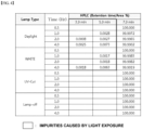
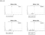
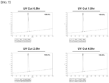
- results of HPLC measurements using the method for evaluating photostability of the present application are shown in FIG. 4 to FIG. 8 .
- impurities caused by light exposure were generated with daylight and white fluorescence, and impurities increased in proportion to the time of light exposure.
- light-denatured impurities were undetected with UV-cut light in the same manner as under the lamp-off condition.
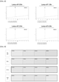
- results of measuring chromaticity using the method for evaluating photostability of the present application are shown in FIG. 9 and FIG. 10 .
- discoloration progressed in proportion to time with the daylight and the white fluorescence similar to the results of HPLC measurements.
- a method for evaluating photostability considering actual light exposure circumstances for a material for an organic material layer of an organic light emitting device may be provided according to one embodiment of the present application.
- an occurrence of denaturation and a degree of denaturation caused by light exposure of the corresponding material for an organic material layer of an organic light emitting device may be quantitatively identified.
Landscapes
- Life Sciences & Earth Sciences (AREA)
- Engineering & Computer Science (AREA)
- Manufacturing & Machinery (AREA)
- Health & Medical Sciences (AREA)
- Analytical Chemistry (AREA)
- Environmental & Geological Engineering (AREA)
- Environmental Sciences (AREA)
- Physics & Mathematics (AREA)
- Biodiversity & Conservation Biology (AREA)
- Chemical & Material Sciences (AREA)
- Ecology (AREA)
- Biochemistry (AREA)
- General Health & Medical Sciences (AREA)
- General Physics & Mathematics (AREA)
- Immunology (AREA)
- Pathology (AREA)
- Electroluminescent Light Sources (AREA)
- Testing Resistance To Weather, Investigating Materials By Mechanical Methods (AREA)
- Investigating, Analyzing Materials By Fluorescence Or Luminescence (AREA)
Abstract
Description
- This application claims priority to and the benefits of
Korean Patent Application No. 10-2020-0168430, filed with the Korean Intellectual Property Office on December 4, 2020 - The present application relates to an apparatus and a method for evaluating photostability of a material for an organic material layer of an organic light emitting device.
- An organic light emitting device is a light emitting device using an organic semiconductor material, and requires an exchange of holes and/or electrons between an electrode and the organic semiconductor material. An organic light emitting device may be largely divided into two types as follows depending on the operation principle. The first is a light emitting device type in which excitons are formed in an organic material layer by photons introduced to a device from an external light source, these excitons are separated into electrons and holes, and these electrons and holes are each transferred to different electrodes and used as a current source (voltage source). The second is a light emitting device type in which, by applying a voltage or current to two or more electrodes, holes and/or electrons are injected into an organic semiconductor material layer forming an interface with the electrodes, and the light emitting device is operated by the injected electrons and holes.
- An organic light emission phenomenon generally refers to a phenomenon converting electrical energy to light energy using an organic material. An organic light emitting device using an organic light emission phenomenon normally has a structure comprising an anode, a cathode, and an organic material layer therebetween. Herein, the organic material layer is often formed in a multilayer structure formed with different materials in order to increase efficiency and stability of the organic light emitting device, and for example, may be formed with a hole injection layer, a hole transfer layer, a light emitting layer, an electron blocking layer, an electron transfer layer, an electron injection layer and the like. When a voltage is applied between the two electrodes in such an organic light emitting device structure, holes and electrons are injected to the organic material layer from the anode and the cathode, respectively, and when the injected holes and electrons meet, excitons are formed, and light emits when these excitons fall back to the ground state. Such an organic light emitting device is known to have properties such as self-emission, high luminance, high efficiency, low driving voltage, wide viewing angle and high contrast.
- Materials used as an organic material layer in an organic light emitting device may be divided into a light emitting material and a charge transfer material, for example, a hole injection material, a hole transfer material, an electron blocking material, an electron transfer material, an electron injection material and the like depending on the function. The light emitting material comprises, depending on light emitting color, blue, green and red light emitting materials, and yellow and orange light emitting materials required for obtaining better natural colors.
- The present application is directed to providing an apparatus and a method for evaluating photostability of a material for an organic material layer of an organic light emitting device.
- One embodiment of the present application provides an apparatus for evaluating photostability of a material for an organic material layer of an organic light emitting device, the apparatus comprising a photostability chamber provided with at least four light source zones,
wherein the at least four light source zones comprise a first light source zone provided with a daylight light source; a second light source zone provided with a white fluorescent light source; a third light source zone provided with a UV-cut light source; and a fourth light source zone to which no light is irradiated. - Another embodiment of the present application provides a method for evaluating photostability of a material for an organic material layer of an organic light emitting device, the method comprising
- preparing the apparatus for evaluating photostability of a material for an organic material layer of an organic light emitting device;
- placing a sample in each of the at least four light source zones;
- irradiating daylight to the first light source zone, irradiating white fluorescence to the second light source zone, irradiating UV-cut light to the third light source zone, and maintaining the fourth light source zone without irradiating separate light thereto; and
- evaluating photostability of the samples by retrieving the samples placed in the at least four light source zones.
- According to one embodiment of the present application, a method for evaluating photostability considering actual light exposure circumstances for a material for an organic material layer of an organic light emitting device can be provided. Particularly, through the apparatus and the method for evaluating photostability according to one embodiment of the present application, an occurrence of denaturation and a degree of denaturation caused by light exposure of the corresponding material for an organic material layer of an organic light emitting device can be quantitatively identified.
- Accordingly, through the apparatus and the method for evaluating photostability according to one embodiment of the present application, changes over time in the material for an organic material layer of an organic light emitting device can be verified in advance, and as a result, the apparatus and the method can become a reliability evaluation standard in the related industry.
-
-
FIG. 1 is a diagram illustrating an apparatus for evaluating photostability of a material for an organic material layer of an organic light emitting device as one embodiment of the present application. -
FIG. 2 is a diagram illustrating wavelength regions of a daylight light source, a white fluorescent light source and a UV-cut light source according to one embodiment of the present application. -
FIG. 3 is a diagram showing a degree of sample discoloration before and after irradiating daylight in Example 1 of the present application. -
FIG. 4 to FIG. 8 are diagrams each showing a result of HPLC measurement using a method for evaluating photostability of the present application. -
FIG. 9 andFIG. 10 are diagrams each showing a result of chromaticity measurement using a method for evaluating photostability of the present application. -
- 10: First Light Source Zone
- 20: Second Light Source Zone
- 30: Third Light Source Zone
- 40: Fourth Light Source Zone
- Hereinafter, the present application will be described in more detail.
- In the present disclosure, a description of a certain member being placed "on" another member comprises not only a case of the certain member being in contact with the another member but a case of still another member being present between the two members.
- In the present disclosure, a description of a certain part "comprising" certain constituents means capable of further comprising other constituents, and does not exclude other constituents unless particularly stated on the contrary.
- As described above, various materials that may be used as an organic material layer of an organic light emitting device have been developed. In addition, the material for an organic material layer of an organic light emitting device has a possibility of being exposed to light and denatured under various environments, however, there are no standardized standards, methods and the like for evaluating photostability of a material for an organic material layer of an organic light emitting device in the art. Accordingly, the present application is directed to providing a method and an apparatus for evaluating photostability considering actual light exposure circumstances for a material for an organic material layer of an organic light emitting device.
- The apparatus for evaluating photostability of a material for an organic material layer of an organic light emitting device according to one embodiment of the present application comprises a photostability chamber provided with at least four light source zones, wherein the at least four light source zones comprise a first light source zone provided with a daylight light source; a second light source zone provided with a white fluorescent light source; a third light source zone provided with a UV-cut light source; and a fourth light source zone to which no light is irradiated.
- In one embodiment of the present application, the at least four light source zones comprise a first light source zone provided with a daylight light source; a second light source zone provided with a white fluorescent light source; a third light source zone provided with a UV-cut light source; and a fourth light source zone to which no light is irradiated.
- The daylight light source of the first light source zone is a substitute for natural light, and considers an environment exposable in a synthesis facility of a material for an organic material layer of an organic light emitting device. The daylight has a color temperature of approximately 4,000K.
- The white fluorescent light source of the second light source zone considers an environment exposable in a synthesis facility of a material for an organic material layer of an organic light emitting device and in a material weighing room of a panel manufacturer. In the present application, the white fluorescent light source may also be referred to as a cool daylight light source, and the color temperature is approximately 6,500K.
- The UV-cut light source of the third light source zone is a UV wavelength-removed light source, and considers an environment exposable in a sublimation facility of a material for an organic material layer of an organic light emitting device and in a manufacturing clean room of a panel manufacturer. The UV-cut light source has a color temperature of approximately 3,000K.
- The fourth light source zone is for comparing with the first light source zone to the third light source zone, and no light is irradiated thereto. The fourth light source zone may not be provided with the daylight light source, the white fluorescent light source and the UV-cut light source, and may be provided with a lamp with the lamp being turned off.
- In addition, there is no chance that the material for an organic material layer of an organic light emitting device is directly exposed to a UV light source in a manufacturing process of the material for an organic material layer of an organic light emitting device and a panel manufacturing process of an organic light emitting device, and therefore, the UV light source may be excluded in one embodiment of the present application.
- Wavelength regions of the daylight light source, the white fluorescent light source and the UV-cut light source according to one embodiment of the present application are shown in
FIG. 2 . - In one embodiment of the present application, the at least four light source zones may each independently be maintained at a temperature of 15°C to 50°C and a humidity of 20% to 90%. In addition, the at least four light source zones may be maintained at a temperature of 25°C and a humidity of 40%, temperature and humidity conditions in a common material manufacturing environment. In addition, the at least four light source zones may each be maintained at constant temperature and humidity, and may all be maintained at the same temperature and humidity. Herein, the temperature deviation may be ±1°C, and the humidity deviation may be ±2%.
- In one embodiment of the present application, the at least four light source zones may each further comprise a shelf on which the sample is placed. Herein, the at least four light source zones are vertically provided in the photostability chamber in consecutive order, and the at least four light source zones may be separated from each other by the shelf.
- The apparatus for evaluating photostability of a material for an organic material layer of an organic light emitting device according to one embodiment of the present application is illustrated in
FIG. 1 . As illustrated inFIG. 1 , the apparatus for evaluating photostability of a material for an organic material layer of an organic light emitting device according to one embodiment of the present application comprises a photostability chamber comprising at least four light source zones, and the at least four light source zones comprise a first light source zone (10) provided with a daylight light source; a second light source zone (20) provided with a white fluorescent light source; a third light source zone (30) provided with a UV-cut light source; and a fourth light source zone (40) to which no light is irradiated. - In addition, the method for evaluating photostability of a material for an organic material layer of an organic light emitting device according to another embodiment of the present application comprises preparing the apparatus for evaluating photostability of a material for an organic material layer of an organic light emitting device; placing a sample in each of the at least four light source zones; irradiating daylight to the first light source zone, irradiating white fluorescence to the second light source zone, irradiating UV-cut light to the third light source zone, and maintaining the fourth light source zone without irradiating separate light thereto; and evaluating photostability of the samples by retrieving the samples placed in the at least four light source zones.
- In the method for evaluating photostability according to one embodiment of the present application, descriptions on the at least four light source zones are the same as the descriptions provided above.
- In one embodiment of the present application, the time of irradiating the daylight, the white fluorescence and the UV-cut light may be from 0.5 hours to 12 hours, and from 0.5 hours to 4 hours.
- In one embodiment of the present application, the evaluating of photostability of the samples may be analyzing chromaticity of the samples, and purity and impurities of the samples. Herein, as for the chromaticity of the samples, CIE L∗a∗b∗ color space may be measured using a spectrophotometer. In addition, the purity and impurities of the samples may be analyzed using HPLC (high-performance liquid chromatography).
- HPLC that analyzes purity and impurities of the samples is an analysis method in which a material dissolved in a solvent, a mobile phase, is separated by a column, a stationary phase, and detected using a proper detector. In the HPLC analysis, an interaction between the material to analyze dissolved in a solvent and the stationary phase is an important factor. In an HPLC analysis of a material for an organic material layer of an organic light emitting device, a stationary phase having a non-polar property and a mobile phase (solvent) having a polar property are generally used. In this case, a material having a polar property is eluted first, and a molecule having lower polarity is eluted after staying in the stationary phase for a long period of time. Using such a principle, samples to analyze pass through an HPLC column, and a material for an organic material layer and other impurities in the samples may be separated and detected.
- Using the above-described method, photostability may be evaluated by comparing purity and impurities for the samples exposed to light in the four light source zones. In addition, the occurrence of light denaturation may be determined by the generation of impurities additionally detected compared to the sample of the fourth light source zone. More specifically, the degree of denaturation is proportional to increases in the number of impurities and the content of impurities, and for the corresponding light source, photostability may be evaluated as low.
- As for the chromaticity of the samples, CIE L∗a∗b∗ values may be analyzed using a spectrophotometer. The L∗ value represents brightness and may be divided into stages from 0 (black) to 100 (white), and having a larger L∗ value means being close to white. The a∗ value represents a relation between red and green, and it is red when having a positive (+) value and green when having a negative (-) value. The b∗ value represents colors of yellow and blue, and it is yellow when having a positive (+) value and blue when having a negative (-) value. Such L∗a∗b∗ values may be derived by analyzing values of reflectivity or transmittance of the samples. The samples are opaque in the analysis of the material for an organic material layer of an organic light emitting device, and the value may be derived by analyzing reflectivity.
- Using the above-described method, photostability may be evaluated by comparing the L∗a∗b∗ values for the samples exposed to light in the four light source zones. In addition, the occurrence of light denaturation may be determined by differences in the L∗a∗b∗ values compared to the sample of the fourth light source zone. The degree of denaturation is proportional as the differences in the L∗a∗b∗ values increase, and photostability for the corresponding light source may be evaluated as low.
- According to one embodiment of the present application, a method for evaluating photostability considering actual light exposure circumstances for a material for an organic material layer of an organic light emitting device may be provided. Particularly, through the apparatus and the method for evaluating photostability according to one embodiment of the present application, an occurrence of denaturation and a degree of denaturation caused by light exposure of the corresponding material for an organic material layer of an organic light emitting device may be quantitatively identified.
- Accordingly, through the apparatus and the method for evaluating photostability according to one embodiment of the present application, changes over time in a material for an organic material layer of an organic light emitting device may be verified in advance, and therefore, the apparatus and the method may become a reliability evaluation standard in the related industry.
- Hereinafter, the present application will be described in detail with reference to examples in order to specifically describe the present application. However, the examples according to the present application may be modified to various different forms, and the scope of the present application is not to be construed as being limited to the examples described below. Examples of the present application are provided in order to more fully describe the present application to those having average knowledge in the art.
- Approximately 1.5 g of a material for an organic material layer of an organic light emitting device (anthracene-based light emitting layer material) was spread as thinly as possible and placed in a transparent Petri dish. The Petri dish was covered with a glass cover to prepare a sample.
- A photostability chamber (VP500L of Votsch Industrietechnik GmbH) as in
FIG. 1 was prepared, and a first light source zone (10) provided with a daylight light source; a second light source zone (20) provided with a white fluorescent light source; a third light source zone (30) provided with a UV-cut light source; and a fourth light source zone (40) to which no light is irradiated by the lamp being turned off. Herein, specific types of the daylight light source, the white fluorescent light source and the UV-cut light source are as follows. - Daylight light source: OSRAM L 18W/640
- White fluorescent light source: Philips TLD 18W/865
- UV-cut light source: Philips TLD 18W/830
- To each of the first light source zone to the fourth light source zone, a minimum of 4 samples were introduced. Temperature and humidity conditions of the first light source zone to the fourth light source zone of the photostability chamber were all set to be the same at 25°C and 40%, and the time of irradiating each light was set at 0.5 hours, 1 hour, 2 hours and 4 hours, and for each time, the samples were taken out from the photostability chamber and analyzed.
- The degrees of discoloration of the samples before and after irradiating daylight in Example 1 are shown in
FIG. 3 . - Results of HPLC measurements using the method for evaluating photostability of the present application are shown in
FIG. 4 to FIG. 8 . As shown in the results ofFIG. 4 to FIG. 8 , impurities caused by light exposure were generated with daylight and white fluorescence, and impurities increased in proportion to the time of light exposure. In addition, light-denatured impurities were undetected with UV-cut light in the same manner as under the lamp-off condition. - Results of measuring chromaticity using the method for evaluating photostability of the present application are shown in
FIG. 9 andFIG. 10 . As shown in the results ofFIG. 9 andFIG. 10 , discoloration progressed in proportion to time with the daylight and the white fluorescence similar to the results of HPLC measurements. In addition, as shown in the results ofFIG. 10 , it was identified that, with daylight and white fluorescence, the L∗ values and the b∗ values changed due to discoloration caused by light exposure. - Accordingly, from the results of Experimental Examples 1 and 2, it was identified that photostability was low under the daylight and white fluorescence conditions since discoloration was identified after 0.5 hours and impurities were generated, and photostability was maintained under the UV-cut light condition.
- As in the results described above, a method for evaluating photostability considering actual light exposure circumstances for a material for an organic material layer of an organic light emitting device may be provided according to one embodiment of the present application. Particularly, through the apparatus and the method for evaluating photostability according to one embodiment of the present application, an occurrence of denaturation and a degree of denaturation caused by light exposure of the corresponding material for an organic material layer of an organic light emitting device may be quantitatively identified.
- Accordingly, through the apparatus and the method for evaluating photostability according to one embodiment of the present application, changes over time in a material for an organic material layer of an organic light emitting device may be verified in advance, and therefore, the apparatus and the method can become a reliability evaluation standard in the related industry.
Claims (12)
- An apparatus for evaluating photostability of a material for an organic material layer of an organic light emitting device, the apparatus comprising a photostability chamber provided with at least four light source zones,
wherein the at least four light source zones comprise a first light source zone provided with a daylight light source; a second light source zone provided with a white fluorescent light source; a third light source zone provided with a UV-cut light source; and a fourth light source zone to which no light is irradiated. - The apparatus for evaluating photostability of a material for an organic material layer of an organic light emitting device of claim 1, wherein the at least four light source zones are each independently maintained at a temperature of 15°C to 50°C and a humidity of 20% to 90%.
- The apparatus for evaluating photostability of a material for an organic material layer of an organic light emitting device of claim 2, wherein the at least four light source zones are all maintained at the same temperature and humidity.
- The apparatus for evaluating photostability of a material for an organic material layer of an organic light emitting device of claim 1, wherein the at least four light source zones each further comprise a shelf on which the sample is placed.
- The apparatus for evaluating photostability of a material for an organic material layer of an organic light emitting device of claim 4, wherein the at least four light source zones are vertically provided in the photostability chamber in consecutive order; and
the at least four light source zones are separated from each other by the shelf. - A method for evaluating photostability of a material for an organic material layer of an organic light emitting device, the method comprising:preparing the apparatus for evaluating photostability of a material for an organic material layer of an organic light emitting device of claim 1;placing a sample in each of the at least four light source zones;irradiating daylight to the first light source zone, irradiating white fluorescence to the second light source zone, irradiating UV-cut light to the third light source zone, and maintaining the fourth light source zone without irradiating separate light thereto; andevaluating photostability of the samples by retrieving the samples placed in the at least four light source zones.
- The method for evaluating photostability of a material for an organic material layer of an organic light emitting device of claim 6, wherein a time of irradiating the daylight, the white fluorescence and the UV-cut light is from 0.5 hours to 12 hours.
- The method for evaluating photostability of a material for an organic material layer of an organic light emitting device of claim 6, wherein the at least four light source zones are each independently maintained at a temperature of 15°C to 50°C and a humidity of 20% to 90%.
- The method for evaluating photostability of a material for an organic material layer of an organic light emitting device of claim 8, wherein the at least four light source zones are all maintained at the same temperature and humidity.
- The method for evaluating photostability of a material for an organic material layer of an organic light emitting device of claim 6, wherein the evaluating of photostability of the samples is analyzing chromaticity of the samples, and purity and impurities of the samples.
- The method for evaluating photostability of a material for an organic material layer of an organic light emitting device of claim 10, wherein the chromaticity of the samples is measuring CIE L∗a∗b∗ color space using a spectrophotometer.
- The method for evaluating photostability of a material for an organic material layer of an organic light emitting device of claim 10, wherein the purity and impurities of the samples are analyzed using HPLC (high-performance liquid chromatography).
Applications Claiming Priority (2)
| Application Number | Priority Date | Filing Date | Title |
|---|---|---|---|
| KR1020200168430A KR102814300B1 (en) | 2020-12-04 | 2020-12-04 | Light stability evaluation apparatus of materials for organic layer of organic light emitting device and evaluation method thereof |
| PCT/KR2021/016792 WO2022119180A1 (en) | 2020-12-04 | 2021-11-16 | Apparatus and method for evaluating light stability of material for organic layer of organic light-emitting element |
Publications (3)
| Publication Number | Publication Date |
|---|---|
| EP4202406A1 true EP4202406A1 (en) | 2023-06-28 |
| EP4202406A4 EP4202406A4 (en) | 2024-02-21 |
| EP4202406B1 EP4202406B1 (en) | 2025-12-31 |
Family
ID=81853236
Family Applications (1)
| Application Number | Title | Priority Date | Filing Date |
|---|---|---|---|
| EP21900868.7A Active EP4202406B1 (en) | 2020-12-04 | 2021-11-16 | DEVICE AND METHOD FOR ASSESSING THE LIGHT STABILITY OF A MATERIAL FOR ORGANIC LAYER OF AN ORGANIC LIGHT-EMISSIVING ELEMENT |
Country Status (7)
| Country | Link |
|---|---|
| US (1) | US20230363247A1 (en) |
| EP (1) | EP4202406B1 (en) |
| JP (1) | JP7452761B2 (en) |
| KR (1) | KR102814300B1 (en) |
| CN (1) | CN116438442A (en) |
| TW (1) | TWI800989B (en) |
| WO (1) | WO2022119180A1 (en) |
Family Cites Families (26)
| Publication number | Priority date | Publication date | Assignee | Title |
|---|---|---|---|---|
| JPS5962542A (en) * | 1982-09-30 | 1984-04-10 | Mitsui Petrochem Ind Ltd | Preparation of purified phenol adduct of 2,2-bis (4-hydroxyphenyl) |
| JPS6056688B2 (en) * | 1982-10-01 | 1985-12-11 | 工業技術院長 | Method for producing oligoalcohol having a hydroxyl group at the end |
| JP3346095B2 (en) * | 1995-05-17 | 2002-11-18 | ミノルタ株式会社 | Spectrophotometer |
| JP2001004526A (en) * | 1999-06-22 | 2001-01-12 | Sony Corp | Light resistance test method and test equipment |
| JP4200815B2 (en) * | 2003-05-19 | 2008-12-24 | セイコーエプソン株式会社 | Durability test apparatus and durability test method |
| DE202005010588U1 (en) * | 2005-07-04 | 2005-10-13 | Weiss Umwelttechnik Gmbh Simulationsanlagen-Messtechnik | Testing chamber for photostability of pharmaceuticals and cosmetics in storage, includes mechanical filter promoting uniform illumination of samples |
| RU2354958C2 (en) * | 2006-09-13 | 2009-05-10 | ООО "Генная и клеточная терапия" | Fluorometric method of determining parametres of photosynthesis of photoautotrophs, device to this end and measuring chamber |
| AR058881A1 (en) | 2006-12-28 | 2008-02-27 | Curtiembres Fonseca S A | DEVICE FOR DEFAULT OF AGING MATERIALS BEFORE THE LIGHT EXHIBITION |
| DE102007002415B4 (en) | 2007-01-17 | 2011-04-28 | Atlas Material Testing Technology Gmbh | Device for light or weathering test comprising a sample housing with integrated UV radiation filter |
| JP2008281392A (en) * | 2007-05-09 | 2008-11-20 | Olympus Corp | Photometric apparatus and automatic analysis apparatus |
| CN101813609A (en) | 2010-04-20 | 2010-08-25 | 北京林业大学 | Test method and device for detecting influence of light wavelength on light-induced discoloration of dyed wood |
| EP2846146B1 (en) * | 2013-09-06 | 2020-01-08 | Atlas Material Testing Technology GmbH | weathering test with multiple independently controllable radiation sources |
| EP3077794A4 (en) * | 2013-12-06 | 2017-12-13 | Bacterioscan Ltd. | Optical measurement cuvette having sample chambers |
| KR20150109542A (en) | 2014-03-19 | 2015-10-02 | 한국생산기술연구원 | Apparatus and method for ultra-highly purifying organic materials for oled purified by ionic liquids |
| CN104007084A (en) | 2014-05-09 | 2014-08-27 | 江苏农牧科技职业学院 | Near-infrared diffuse-reflection rapid nondestructive testing apparatus for organophosphorus pesticide residues |
| CN204359664U (en) * | 2014-12-11 | 2015-05-27 | 绵阳佳联印染有限责任公司 | A kind of solarization climate test machine |
| US9696434B2 (en) | 2015-06-04 | 2017-07-04 | Toshiba Medical Systems Corporation | Scintillator array test method, apparatus, and system |
| JP3203769U (en) * | 2016-02-04 | 2016-04-14 | 株式会社日本医化器械製作所 | Light stability test equipment |
| KR101881225B1 (en) * | 2016-11-30 | 2018-07-24 | 주식회사 맥사이언스 | Solar Simulator Using Flash Lamp |
| CN106706507A (en) * | 2017-01-17 | 2017-05-24 | 同济大学 | Method for testing ultraviolet aging performance of bituminous mixture |
| US11088328B2 (en) * | 2017-04-04 | 2021-08-10 | Semiconductor Energy Laboratory Co., Ltd. | Method of analyzing organic semiconductor element |
| CN206862852U (en) * | 2017-07-12 | 2018-01-09 | 北京北化高科新技术股份有限公司 | A kind of pigment weatherability tape deck |
| KR102411607B1 (en) * | 2017-10-13 | 2022-06-22 | 삼성디스플레이 주식회사 | Inspecting method of display panel |
| CN108956486B (en) * | 2018-08-21 | 2022-03-11 | 海南金海浆纸业有限公司 | A Dye Evaluation Method |
| GB2581363A (en) | 2019-02-14 | 2020-08-19 | Univ Exeter | Test apparatus |
| CN111999445A (en) | 2020-09-03 | 2020-11-27 | 广东中科英海科技有限公司 | Natural enemy insect acute toxicity test exposure device |
-
2020
- 2020-12-04 KR KR1020200168430A patent/KR102814300B1/en active Active
-
2021
- 2021-11-16 WO PCT/KR2021/016792 patent/WO2022119180A1/en not_active Ceased
- 2021-11-16 CN CN202180065197.5A patent/CN116438442A/en active Pending
- 2021-11-16 EP EP21900868.7A patent/EP4202406B1/en active Active
- 2021-11-16 US US18/026,176 patent/US20230363247A1/en active Pending
- 2021-11-16 JP JP2023515276A patent/JP7452761B2/en active Active
- 2021-11-18 TW TW110142857A patent/TWI800989B/en active
Also Published As
| Publication number | Publication date |
|---|---|
| CN116438442A (en) | 2023-07-14 |
| JP7452761B2 (en) | 2024-03-19 |
| KR20220079037A (en) | 2022-06-13 |
| EP4202406A4 (en) | 2024-02-21 |
| US20230363247A1 (en) | 2023-11-09 |
| TW202235848A (en) | 2022-09-16 |
| JP2023540780A (en) | 2023-09-26 |
| KR102814300B1 (en) | 2025-05-28 |
| TWI800989B (en) | 2023-05-01 |
| EP4202406B1 (en) | 2025-12-31 |
| WO2022119180A1 (en) | 2022-06-09 |
Similar Documents
| Publication | Publication Date | Title |
|---|---|---|
| Seifert et al. | Chemical degradation mechanisms of highly efficient blue phosphorescent emitters used for organic light emitting diodes | |
| Ding et al. | Direct blending of multicolor carbon quantum dots into fluorescent films for white light emitting diodes with an adjustable correlated color temperature | |
| Granström et al. | White light emission from a polymer blend light emitting diode | |
| Sun et al. | Azasiline-based thermally activated delayed fluorescence emitters for blue organic light emitting diodes | |
| de Moraes et al. | Analysis of chemical degradation mechanism within sky blue phosphorescent organic light emitting diodes by laser-desorption/ionization time-of-flight mass spectrometry | |
| EP2388843A2 (en) | Organic material and organic light emitting diode display using same | |
| US20230266247A1 (en) | Metrology for oled manufacturing using photoluminescence spectroscopy | |
| KR20170115498A (en) | Organic EL Light Emitting Device and Electronic Apparatus | |
| CN1325431A (en) | Electrolumiscent materials | |
| Ohno | Optical metrology for LEDs and solid state lighting | |
| De Moraes et al. | Chemical degradation processes of highly stable red phosphorescent organic light emitting diodes | |
| EP4202406B1 (en) | DEVICE AND METHOD FOR ASSESSING THE LIGHT STABILITY OF A MATERIAL FOR ORGANIC LAYER OF AN ORGANIC LIGHT-EMISSIVING ELEMENT | |
| Popp et al. | High performance two-color hybrid TADF-phosphorescent WOLEDs with bimodal Förster and Dexter-type exciton distribution | |
| Danyliv et al. | Effects of the nature of donor substituents on the photophysical and electroluminescence properties of derivatives of perfluorobiphenyl: donor–acceptor versus donor–acceptor–donor type AIEE/TADF emitters | |
| Wölzl et al. | Performance and lifetime of vacuum deposited organic light-emitting diodes: Influence of residual gases present during device fabrication | |
| Kirch et al. | Accurate wavelength tracking by exciton spin mixing | |
| Srividya et al. | White light source towards spectrum tunable lighting—A review | |
| Lub et al. | On the photo-oxidation of perylene bisimide dyes in alcoholic solutions | |
| Jou et al. | Pseudo‐natural Light for Displays and Lighting | |
| Winter et al. | Photoluminescence degradation of blue OLED emitters | |
| de Moraes et al. | Influence of the applied charge on the electro-chemical degradation in green phosphorescent organic light emitting diodes | |
| de Fonjaudran et al. | Optical and theoretical investigation of Indian yellow (euxanthic acid and euxanthone) | |
| Mandal et al. | Luminescent quantum counters based on organic dyes in polymer matrixes | |
| CN113357569B (en) | Multi-primary-color LED light-emitting system | |
| US11984053B2 (en) | Display device and method of driving display device |
Legal Events
| Date | Code | Title | Description |
|---|---|---|---|
| STAA | Information on the status of an ep patent application or granted ep patent |
Free format text: STATUS: THE INTERNATIONAL PUBLICATION HAS BEEN MADE |
|
| PUAI | Public reference made under article 153(3) epc to a published international application that has entered the european phase |
Free format text: ORIGINAL CODE: 0009012 |
|
| STAA | Information on the status of an ep patent application or granted ep patent |
Free format text: STATUS: REQUEST FOR EXAMINATION WAS MADE |
|
| 17P | Request for examination filed |
Effective date: 20230323 |
|
| AK | Designated contracting states |
Kind code of ref document: A1 Designated state(s): AL AT BE BG CH CY CZ DE DK EE ES FI FR GB GR HR HU IE IS IT LI LT LU LV MC MK MT NL NO PL PT RO RS SE SI SK SM TR |
|
| A4 | Supplementary search report drawn up and despatched |
Effective date: 20240122 |
|
| RIC1 | Information provided on ipc code assigned before grant |
Ipc: H10K 71/70 20230101ALI20240116BHEP Ipc: G01N 17/00 20060101AFI20240116BHEP |
|
| DAV | Request for validation of the european patent (deleted) | ||
| DAX | Request for extension of the european patent (deleted) | ||
| GRAP | Despatch of communication of intention to grant a patent |
Free format text: ORIGINAL CODE: EPIDOSNIGR1 |
|
| STAA | Information on the status of an ep patent application or granted ep patent |
Free format text: STATUS: GRANT OF PATENT IS INTENDED |
|
| INTG | Intention to grant announced |
Effective date: 20250919 |
|
| GRAS | Grant fee paid |
Free format text: ORIGINAL CODE: EPIDOSNIGR3 |
|
| GRAA | (expected) grant |
Free format text: ORIGINAL CODE: 0009210 |
|
| STAA | Information on the status of an ep patent application or granted ep patent |
Free format text: STATUS: THE PATENT HAS BEEN GRANTED |
|
| AK | Designated contracting states |
Kind code of ref document: B1 Designated state(s): AL AT BE BG CH CY CZ DE DK EE ES FI FR GB GR HR HU IE IS IT LI LT LU LV MC MK MT NL NO PL PT RO RS SE SI SK SM TR |
|
| REG | Reference to a national code |
Ref country code: CH Ref legal event code: F10 Free format text: ST27 STATUS EVENT CODE: U-0-0-F10-F00 (AS PROVIDED BY THE NATIONAL OFFICE) Effective date: 20251231 Ref country code: GB Ref legal event code: FG4D |
|
| REG | Reference to a national code |
Ref country code: DE Ref legal event code: R096 Ref document number: 602021045759 Country of ref document: DE |
|
| REG | Reference to a national code |
Ref country code: IE Ref legal event code: FG4D |
|
| REG | Reference to a national code |
Ref country code: LT Ref legal event code: MG9D |
|
| PG25 | Lapsed in a contracting state [announced via postgrant information from national office to epo] |
Ref country code: NO Free format text: LAPSE BECAUSE OF FAILURE TO SUBMIT A TRANSLATION OF THE DESCRIPTION OR TO PAY THE FEE WITHIN THE PRESCRIBED TIME-LIMIT Effective date: 20260331 |
|
| PG25 | Lapsed in a contracting state [announced via postgrant information from national office to epo] |
Ref country code: HR Free format text: LAPSE BECAUSE OF FAILURE TO SUBMIT A TRANSLATION OF THE DESCRIPTION OR TO PAY THE FEE WITHIN THE PRESCRIBED TIME-LIMIT Effective date: 20251231 Ref country code: FI Free format text: LAPSE BECAUSE OF FAILURE TO SUBMIT A TRANSLATION OF THE DESCRIPTION OR TO PAY THE FEE WITHIN THE PRESCRIBED TIME-LIMIT Effective date: 20251231 |
|
| PG25 | Lapsed in a contracting state [announced via postgrant information from national office to epo] |
Ref country code: RS Free format text: LAPSE BECAUSE OF FAILURE TO SUBMIT A TRANSLATION OF THE DESCRIPTION OR TO PAY THE FEE WITHIN THE PRESCRIBED TIME-LIMIT Effective date: 20260331 |
|
| PG25 | Lapsed in a contracting state [announced via postgrant information from national office to epo] |
Ref country code: LV Free format text: LAPSE BECAUSE OF FAILURE TO SUBMIT A TRANSLATION OF THE DESCRIPTION OR TO PAY THE FEE WITHIN THE PRESCRIBED TIME-LIMIT Effective date: 20251231 |
|
| PG25 | Lapsed in a contracting state [announced via postgrant information from national office to epo] |
Ref country code: BG Free format text: LAPSE BECAUSE OF FAILURE TO SUBMIT A TRANSLATION OF THE DESCRIPTION OR TO PAY THE FEE WITHIN THE PRESCRIBED TIME-LIMIT Effective date: 20251231 |
|
| REG | Reference to a national code |
Ref country code: NL Ref legal event code: MP Effective date: 20251231 |