EP4199117A1 - Semiconductor device, and preparation method therefor and use thereof - Google Patents
Semiconductor device, and preparation method therefor and use thereof Download PDFInfo
- Publication number
- EP4199117A1 EP4199117A1 EP22712487.2A EP22712487A EP4199117A1 EP 4199117 A1 EP4199117 A1 EP 4199117A1 EP 22712487 A EP22712487 A EP 22712487A EP 4199117 A1 EP4199117 A1 EP 4199117A1
- Authority
- EP
- European Patent Office
- Prior art keywords
- material layer
- substrate
- semiconductor material
- semiconductor device
- semiconductor
- Prior art date
- Legal status (The legal status is an assumption and is not a legal conclusion. Google has not performed a legal analysis and makes no representation as to the accuracy of the status listed.)
- Granted
Links
Images






Classifications
-
- H—ELECTRICITY
- H10—SEMICONDUCTOR DEVICES; ELECTRIC SOLID-STATE DEVICES NOT OTHERWISE PROVIDED FOR
- H10D—INORGANIC ELECTRIC SEMICONDUCTOR DEVICES
- H10D30/00—Field-effect transistors [FET]
- H10D30/60—Insulated-gate field-effect transistors [IGFET]
- H10D30/791—Arrangements for exerting mechanical stress on the crystal lattice of the channel regions
- H10D30/797—Arrangements for exerting mechanical stress on the crystal lattice of the channel regions being in source or drain regions, e.g. SiGe source or drain
-
- H—ELECTRICITY
- H10—SEMICONDUCTOR DEVICES; ELECTRIC SOLID-STATE DEVICES NOT OTHERWISE PROVIDED FOR
- H10D—INORGANIC ELECTRIC SEMICONDUCTOR DEVICES
- H10D30/00—Field-effect transistors [FET]
- H10D30/01—Manufacture or treatment
- H10D30/021—Manufacture or treatment of FETs having insulated gates [IGFET]
- H10D30/027—Manufacture or treatment of FETs having insulated gates [IGFET] of lateral single-gate IGFETs
-
- H—ELECTRICITY
- H10—SEMICONDUCTOR DEVICES; ELECTRIC SOLID-STATE DEVICES NOT OTHERWISE PROVIDED FOR
- H10D—INORGANIC ELECTRIC SEMICONDUCTOR DEVICES
- H10D30/00—Field-effect transistors [FET]
- H10D30/60—Insulated-gate field-effect transistors [IGFET]
- H10D30/601—Insulated-gate field-effect transistors [IGFET] having lightly-doped drain or source extensions, e.g. LDD IGFETs or DDD IGFETs
-
- H—ELECTRICITY
- H10—SEMICONDUCTOR DEVICES; ELECTRIC SOLID-STATE DEVICES NOT OTHERWISE PROVIDED FOR
- H10D—INORGANIC ELECTRIC SEMICONDUCTOR DEVICES
- H10D30/00—Field-effect transistors [FET]
- H10D30/60—Insulated-gate field-effect transistors [IGFET]
- H10D30/751—Insulated-gate field-effect transistors [IGFET] having composition variations in the channel regions
-
- H—ELECTRICITY
- H10—SEMICONDUCTOR DEVICES; ELECTRIC SOLID-STATE DEVICES NOT OTHERWISE PROVIDED FOR
- H10D—INORGANIC ELECTRIC SEMICONDUCTOR DEVICES
- H10D84/00—Integrated devices formed in or on semiconductor substrates that comprise only semiconducting layers, e.g. on Si wafers or on GaAs-on-Si wafers
- H10D84/01—Manufacture or treatment
- H10D84/0123—Integrating together multiple components covered by H10D12/00 or H10D30/00, e.g. integrating multiple IGBTs
- H10D84/0126—Integrating together multiple components covered by H10D12/00 or H10D30/00, e.g. integrating multiple IGBTs the components including insulated gates, e.g. IGFETs
- H10D84/0165—Integrating together multiple components covered by H10D12/00 or H10D30/00, e.g. integrating multiple IGBTs the components including insulated gates, e.g. IGFETs the components including complementary IGFETs, e.g. CMOS devices
- H10D84/0167—Manufacturing their channels
-
- H—ELECTRICITY
- H10—SEMICONDUCTOR DEVICES; ELECTRIC SOLID-STATE DEVICES NOT OTHERWISE PROVIDED FOR
- H10D—INORGANIC ELECTRIC SEMICONDUCTOR DEVICES
- H10D84/00—Integrated devices formed in or on semiconductor substrates that comprise only semiconducting layers, e.g. on Si wafers or on GaAs-on-Si wafers
- H10D84/01—Manufacture or treatment
- H10D84/02—Manufacture or treatment characterised by using material-based technologies
- H10D84/03—Manufacture or treatment characterised by using material-based technologies using Group IV technology, e.g. silicon technology or silicon-carbide [SiC] technology
- H10D84/038—Manufacture or treatment characterised by using material-based technologies using Group IV technology, e.g. silicon technology or silicon-carbide [SiC] technology using silicon technology, e.g. SiGe
-
- G—PHYSICS
- G11—INFORMATION STORAGE
- G11C—STATIC STORES
- G11C8/00—Arrangements for selecting an address in a digital store
- G11C8/08—Word line control circuits, e.g. drivers, boosters, pull-up circuits, pull-down circuits, precharging circuits, for word lines
Definitions
- the disclosure relates to the technical field of the semiconductor, in particular to a semiconductor device, a method for manufacturing same and application thereof.
- MOS metal oxide semiconductor
- embodiments of the disclosure provide a semiconductor device, a method for manufacturing it and an application thereof.
- a semiconductor device includes a substrate; a semiconductor material layer located on the substrate and covering part of the substrate; a gate located on the semiconductor material layer and the substrate not covered by the semiconductor material layer; in which along an extension direction of the gate, a width of the semiconductor material layer is smaller than a width of the substrate, and a carrier mobility of a material of the semiconductor material layer is different from a carrier mobility of a material of the substrate.
- the material of the substrate includes a first element
- the material of the semiconductor material layer includes the first element and a second element different from the first element
- the first element is silicon and the second element is germanium.
- a percentage content of the second element in the semiconductor material layer ranges from 20% to 40%.
- the semiconductor device includes three states, and in the case that a voltage applied to the semiconductor device is less than a first threshold, the semiconductor device is in an off state; in the case that the voltage is greater than the first threshold and less than a second threshold, the semiconductor device is in a semi-conducting state; in the case that the voltage is greater than the second threshold, the semiconductor device is in a full-conducting state.
- the semiconductor device further includes: a source and a drain, which are respectively located on both sides of the gate and penetrate through the semiconductor material layer and extend into the substrate.
- a method for manufacturing a semiconductor device includes: providing a substrate; forming a semiconductor material layer on the substrate, in which the semiconductor material layer covers a part of the substrate; forming a gate on the semiconductor material layer and the substrate not covered by the semiconductor material layer; in which, along an extension direction of the gate, a width of the semiconductor material layer is smaller than a width of the substrate, and a carrier mobility of a material of the semiconductor material layer is different from a carrier mobility of a material of the substrate.
- the material of the substrate includes a first element
- the material of the semiconductor material layer includes the first element and a second element different from the first element
- the first element is silicon and the second element is germanium.
- a percentage content of the second element in the semiconductor material layer ranges from 20% to 40%.
- the semiconductor material layer is formed by an in-situ doping epitaxial process, in which growth rates of the semiconductor material layer in a middle area and an edge area of the substrate are adjusted by controlling a flow rate of a growth gas, so that the semiconductor material layer covers a part of the substrate.
- a photoresist layer is formed on a mask layer covering the substrate.
- the photoresist layer is exposed and developed to transfer a preset pattern of the semiconductor material layer in a photomask to the photoresist layer.
- a portion of the mask layer corresponding to the preset pattern of the semiconductor material layer is removed to expose part of the substrate.
- the semiconductor material layer is formed on the exposed substrate.
- the method further includes: Ion doping is carried out on the semiconductor material layer on both sides of the gate and the substrate under the semiconductor material layer to form a source and a drain penetrating through the semiconductor material layer and extending into the substrate.
- an application of a semiconductor device in a circuit includes: a main word line, a sub word line, a word line driving circuit and a voltage control module, in which the voltage control module includes the semiconductor device as described in anyone of the above embodiments.
- the semiconductor device includes a source terminal, a drain terminal and a gate terminal; the source terminal is connected to a high-level signal, the drain terminal is connected to a main word line, and the gate terminal is connected to a standby signal.
- the word line driving circuit is connected between the main word line and the sub word line.
- the voltage control module is configured to reduce a voltage output to the word line driving circuit in the case that a standby state occurs.
- the word line driving circuit includes a first PMOS transistor, a first NMOS transistor and a second NMOS transistor; the gates of the first PMOS transistor and the first NMOS transistor are connected and are connected to the main word line; the source of the first NMOS transistor and the source of the second NMOS transistor are connected and are grounded; the drain of the first PMOS transistor, the drain of the first NMOS transistor and the drain of the second NMOS transistor are connected and are connected to the sub word line.
- a method for driving a circuit is provided, the method for driving a circuit is applied to the circuit described in anyone of the embodiments of the third aspect of the disclosure; the method includes: controlling the semiconductor device to be in the off state in the case that the standby state does not occur; and controlling the semiconductor device to be in the semi-conducting state in the case that the standby state occurs, so as to increase an equivalent resistance of the semiconductor device and reduce a voltage output to the word line driving circuit.
- a control device with at least three states is provided, which at least includes three states of off, semi-conducting and full-conducting. In practical circuit application, it can switch various working states according to the voltage and reduce GIDL current.
- the first element, component, region, layer or part discussed below can be expressed as the second element, component, region, layer or part without departing from the teachings of the disclosure.
- the second element, component, region, layer or part it does not mean that the first element, component, region, layer or part necessarily exists in this disclosure.
- Spatial terms such as under, below, the lower, beneath, on, above, etc. can be used here to describe the relationship between one element or feature shown in the figure and other elements or features. It should be understood that in addition to the orientations shown in the figures, the spatial relationship term is intended to include different orientations of devices in use and operation. For example, if the device in the drawing is flipped over, then the element or feature described as “under other elements” or “under them” or “below them” will be oriented to be “above” other elements or features. Therefore, the exemplary terms “under ...” and “below " may include both the up and down orientations. The device can be otherwise oriented (rotated by 90 degrees or other orientations) and the spatial descriptors used herein should be interpreted accordingly.
- FIG. 1 is a top view of a semiconductor device provided by an embodiment of the disclosure
- FIG. 2 is a cross-sectional view along the dotted line A-A' in FIG. 1
- FIG. 3 is a cross-sectional view along the dotted line B-B' in FIG. 1 .
- the semiconductor device includes: a substrate 10; a semiconductor material layer 20 located on the substrate 10 and covering a part of the substrate 10; a gate 30 located on the semiconductor material layer 20 and the substrate 10 not covered by the semiconductor material layer 20; in which a width of the semiconductor material layer 20 is smaller than a width of the substrate 10 along an extending direction of the gate 30, and a carrier mobility of the material of the semiconductor material layer 20 and a carrier mobility of the material of the substrate 10 are different.
- a control device with at least three states is provided, which at least includes three states of off, semi-conducting and full-conducting. In practical circuit application, it can switch various working states according to the voltage and reduce GIDL current.
- the substrate 10 may be an elementary semiconductor material substrate (such as silicon (Si) substrate, germanium (Ge) substrate, etc.), a composite semiconductor material substrate (such as silicon germanium (SiGe) substrate, etc.), or a silicon-on-insulator (SOI) substrate, germanium-on-insulator (GeOI) substrate, etc.
- the substrate 10 is a silicon substrate.
- the carrier mobility of the semiconductor material layer 20 is greater than the carrier mobility of the substrate 10 material, thus improving the carrier mobility of the channel region, optimizing the operation speed of the semiconductor device and improving the electrical performance of the semiconductor device.
- the gate 30 may include an oxide layer, a first gate conductive layer, a second gate conductive layer and other structures (not shown in the figures) stacked in sequence.
- the width of the semiconductor material layer 20 is smaller than the width of the substrate 10 along the direction perpendicular to the extension of the gate 30. In other embodiments, the width of the semiconductor material layer 20 may be equal to the width of the substrate 10 along a direction perpendicular to the extension of the gate 30.
- the material of the substrate 10 includes a first element
- the material of the semiconductor material layer 20 includes the first element and a second element different from the first element.
- the first element is silicon and the second element is germanium. That is, the substrate 10 is a silicon substrate, and the semiconductor material layer 20 is a germanium silicon layer. There is a lattice difference between germanium and silicon, by which the carrier mobility may be affected and thus the threshold voltage of the channel region is adjusted.
- the first element and the second element may also be selected from other elements that can affect the carrier mobility, such as but not limited to silicon, germanium, boron, tellurium, iodine, carbon, phosphorus, arsenic, sulfur and the like.
- the substrate 10 is a silicon substrate
- the semiconductor material layer 20 is a germanium silicon layer containing carbon.
- a percentage content of the second element in the semiconductor material layer 20 ranges from 20% to 40%. Therefore, in the range, the semiconductor material layer can better influence the carrier mobility and adjust the threshold voltage of the channel region, so that the formed third-stage control device can better reduce the GIDL current.
- the semiconductor material layer 20 includes a first semiconductor material layer and a second semiconductor material layer (not shown in the figures).
- the first semiconductor material layer and the second semiconductor material layer are arranged side by side, and both the first semiconductor material layer and the second semiconductor material layer extend along the direction from the source to the drain.
- the mobility of the material of the first semiconductor material layer, the mobility of the material of the second semiconductor material layer and the mobility of the material of the substrate are different. In this way, according to the difference in carrier mobility of the first semiconductor material layer, the second semiconductor material layer and the substrate, the semiconductor device can be formed into a device with more states.
- the length of the gate 30 is longer than the length of the substrate 10 along the extending direction of the gate 30, that is, the gate 30 may be located on other structures, so the length of the gate 30 is longer than the length of the substrate 10. In this way, the control ability of the channel region can be improved, and the leakage problem of devices can be improved, meanwhile multiple device structures can share the same gate.
- the semiconductor device includes three states. When the voltage applied to the semiconductor device is less than a first threshold, the semiconductor device is in the off state. When the voltage is greater than the first threshold and less than a second threshold, the semiconductor device is in a semi-conducting state. When the voltage is greater than the second threshold, the semiconductor device is in a full-conducting state.
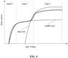
- the channel region of the semiconductor device is divided into two parts, one part is the middle area covered by the semiconductor material layer 20, and the other part is the edge area not covered by the semiconductor material layer 20. Since the semiconductor material layer 20 only partially grows on the substrate 10, the threshold voltage of the channel region in the middle area covered by the semiconductor material layer 20 is low, and the middle area can be turned on in advance. When the voltage reaches the threshold voltage of the edge area, the channel in the edge area can be turned on. Finally the voltage versus current curve formed is shown in FIG. 4 .
- the voltage of the semiconductor device is less than the first threshold, and neither the middle area nor the edge area reaches the on state, so the semiconductor device is in the off state; in stage 1, the voltage of the semiconductor device is greater than the first threshold and less than the second threshold, and the middle region reaches the on state, while the edge area is still in the off state, so the semiconductor device is in the semi-conducting state, and redundancy to the gate voltage is high, and the drain current does not change due to slight fluctuation of the gate voltage; in stage 2, the voltage of the semiconductor device is greater than the second threshold, and both the middle area and the edge area reach the on state, so the semiconductor device is in the full-conducting state and operates in the saturation region.
- the three states of the semiconductor device are shown by the dotted line in FIG. 4 .
- the semiconductor device provided by an embodiment of the disclosure is a control device with three states.
- the semiconductor device further includes a source 41 and a drain 42, which are located on both sides of the gate 30 and penetrate through the semiconductor material layer 20 and extend into the substrate 10.
- a method for manufacturing a semiconductor device is also provided.
- the method includes the following operations.
- a substrate is provided.
- a semiconductor material layer is formed on the substrate, in which the semiconductor material layer covers a part of the substrate.
- a gate is formed on the semiconductor material layer and the substrate not covered by the semiconductor material layer, in which, along the extending direction of the gate, the width of the semiconductor material layer is smaller than the width of the substrate, and the carrier mobility of the material of the semiconductor material layer is different from the carrier mobility of the material of the substrate.
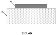
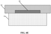
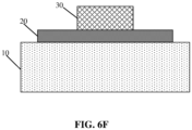
- Figs. 6A to 6G are schematic structural diagrams of a semiconductor device provided by the embodiment of the disclosure in the manufacturing process.
- FIGs. 6A to 6E are sectional views along the dotted line B-B' in FIG. 1
- FIGs. 6F to 6G are sectional views along the dotted line A-A' in FIG. 1 .
- the substrate 10 may be an elementary semiconductor material substrate (such as silicon (Si) substrate, germanium (Ge) substrate, etc.), a composite semiconductor material substrate (such as silicon germanium (SiGe) substrate, etc.), or a silicon-on-insulator (SOI) substrate, germanium-on-insulator (GeOI) substrate, etc.
- the substrate 10 is the silicon substrate.
- the operation 502 is performed.
- a semiconductor material layer 20 is formed on the substrate 10, and the semiconductor material layer 20 covers a part of the substrate 10.
- a mask layer 50 may be formed on the substrate 10 firstly, and then a photoresist layer 60 may be formed on the mask layer 50 covering the substrate 10.
- the mask layer 50 may be a composite material layer of silicon dioxide and silicon nitride.
- the photoresist layer 60 is exposed and developed to transfer a preset pattern of the semiconductor material layer on a photomask (not shown in the figure) to the photoresist layer 60, forming a patterned photoresist layer.
- the part of the mask layer 50 corresponding to the preset pattern of the semiconductor material layer is etched to expose a part of the substrate 10.
- the mask layer and the photoresist layer located in the middle area of the substrate 10 are removed to expose the middle area of the substrate 10.
- the photoresist layer 60 is a positive photoresist or a negative photoresist.
- the positive photoresist may form soluble substances after illumination, while the negative photoresist forms insoluble substances after illumination.
- the semiconductor material layer 20 is formed on the exposed substrate 10. After forming the semiconductor material layer 20, the remaining photoresist layer 60 and mask layer 50 are removed.
- the photomask for forming the semiconductor material layer may be formed by modifying the photomask in the previous process, such as a PMOS mask, without adding a new photomask. In this way, the process can be reduced and the cost can be saved.
- the semiconductor material layer 20 is formed by a method for forming the photoresist layer, and in other embodiments, the semiconductor material layer 20 may also be formed by an in-situ doping epitaxial process.
- the semiconductor material layer 20 is formed by the in-situ doping epitaxial process, in which growth rates of the semiconductor material layer 20 in the middle area and the edge area of the substrate 10 are adjusted by controlling the flow rate of growth gas, so as to make the semiconductor material layer 20 cover a part of the substrate 10.
- the growth gas includes HCL, SiH 4 and GeH 4 .
- Different percentage contents of germanium atoms can be obtained by adjusting the flow ratio of HCL, SiH 4 and GeH 4 , and the germanium atoms are evenly distributed, the process step is simple, and the uniformity of the formed semiconductor material layer is good.
- the material of the substrate 10 includes a first element
- the material of the semiconductor material layer 20 includes the first element and a second element different from the first element.
- the first element is silicon and the second element is germanium. That is, the substrate 10 is a silicon substrate, and the semiconductor material layer 20 is a germanium silicon layer. There is a lattice difference between germanium and silicon, by which the carrier mobility can be affected and thus the threshold voltage of the channel region is adjusted.
- the first element and the second element may also be selected from other elements that can affect the carrier mobility, such as but not limited to silicon, germanium, boron, tellurium, iodine, carbon, phosphorus, arsenic, sulfur and the like.
- the substrate 10 is a silicon substrate
- the semiconductor material layer 20 is a germanium silicon layer containing carbon.
- a percentage content of the second element in the semiconductor material layer ranges from 20% to 40%. Therefore, in the range, the semiconductor material layer can better influence the carrier mobility and adjust the threshold voltage of the channel region, so that the formed control device with three states can better reduce the GIDL current.
- FIG. 6E is a sectional view along the dotted line B-B' in FIG. 1
- FIG. 6F is a sectional view along the dotted line A-A' in FIG. 1 .
- the operation 503 is performed, a gate 30 is formed on the semiconductor material layer 20 and the substrate 10 not covered by the semiconductor material layer 20; in which the width of the semiconductor material layer 20 is smaller than the width of the substrate 10 along the extending direction of the gate 30, and the carrier mobility of the material of the semiconductor material layer 20 is different from that of the substrate 10.
- the carrier mobility of the semiconductor material layer 20 is greater than the carrier mobility of the material of the substrate 10, thus improving the carrier mobility of the channel region, optimizing the operation speed of the semiconductor device and improving the electrical performance of the semiconductor device.
- the formation of the gate 30 specifically includes: firstly, a mask layer (not shown in the figures) can be formed on the semiconductor material layer 20 and the substrate 10 not covered by the semiconductor material layer 20, and then the mask layer is patterned, to bring out the gate trench pattern to be etched in the mask layer, and the mask layer may be patterned by photolithography technique.
- the mask layer may be a photoresist mask or a hard mask patterned based on a photolithography mask.
- the mask layer is specifically patterned through the operations of exposure, development, removing of photoresist and the like.
- the gate trench with a certain depth is etched according to the pattern of the gate trench to be etched.
- the gate is formed in the gate trench, and the redundant mask layer is removed.
- the gate 30 may include an oxide layer, a first gate conductive layer, a second gate conductive layer and other structures (not shown in the figures) stacked in sequence.
- the semiconductor device includes three states, and when a voltage applied to the semiconductor device is less than a first threshold, the semiconductor device is in an off state; when the voltage is greater than the first threshold and less than a second threshold, the semiconductor device is in a semi-conducting state; when the voltage is greater than the second threshold, the semiconductor device is in a fully full-conducting state.
- the channel region of the semiconductor device is divided into two parts, one part is the middle area covered by the semiconductor material layer 20, and the other part is the edge area not covered by the semiconductor material layer 20. Since the semiconductor material layer 20 only grows on part of the substrate 10, the threshold voltage of the channel region in the middle region covered by the semiconductor material layer 20 is relatively low, and the middle area will be turned on in advance. When the voltage reaches the threshold voltage of the edge area, the channel in the edge area is turned on. Finally, the voltage versus current curve formed is shown in FIG. 4 .
- the voltage of the semiconductor device is less than the first threshold, and neither the middle area nor the edge area reaches the on state, so the semiconductor device is in the off state; in stage 1, the voltage of the semiconductor device is greater than the first threshold and less than the second threshold, and the middle region reaches the on state, while the edge area is still in the off state, so the semiconductor device is in the semi-conducting state, and redundancy to the gate voltage is high, and the drain current does not change due to slight fluctuation of the gate voltage; in stage 2, the voltage of the semiconductor device is greater than the second threshold, and both the middle area and the edge area reach the on state, and thus the semiconductor device is in full-conducting state and operates in the saturation region.
- the three states of the semiconductor device are shown by the broken line in FIG. 4 . Therefore, the semiconductor device provided by the embodiment of this disclosure is a control device with three states.
- the length of the gate 30 is greater than the length of the substrate 10 along the extending direction of the gate 30, that is, the gate 30 may be located on other structures, and thus the length of the gate 30 is greater than the length of the substrate 10. In this way, the control ability of the channel region can be improved, and the device leakage problem can be improved; meanwhile multiple device structures can share the same gate.
- the semiconductor material layer 20 on both sides of the gate 30 and the substrate 10 under the semiconductor material layer 20 are ion doped to form the source 41 and the drain 42 penetrating through the semiconductor material layer 20 and extending into the substrate 10.
- a lightly doped drain region implantation process LDD
- S/D source/drain region
- an annealing process may be sequentially performed, so that the source 41 and the drain 42 are formed on both sides of the gate 30; the specific process parameters may be set according to actual process requirements, which is not limited in this disclosure.
- the semiconductor material layer 20 includes a first semiconductor material layer and a second semiconductor material layer (not shown in the figures).
- the first semiconductor material layer and the second semiconductor material layer are arranged side by side, and both the first semiconductor material layer and the second semiconductor material layer extend along the direction from the source to the drain.
- the mobility of the material of the first semiconductor material layer, the mobility of the material of the second semiconductor material layer and the mobility of the material of the substrate are different. In this way, according to the difference in carrier mobility of the first semiconductor material layer, the second semiconductor material layer and the substrate, the semiconductor device can be formed into a device with more states.
- a circuit is further provided, in which the above semiconductor device is applied.
- the circuit includes: a main word line MWL, a sub word line WL, a word line driving circuit 71 and a voltage control module 72, and the voltage control module 72 includes the semiconductor device 721 as described in anyone of the above embodiments.
- the semiconductor device 721 includes a source terminal, a drain terminal and a gate terminal.
- the source terminal is connected to the high level signal VPP
- the drain terminal is connected to the main word line MWL
- the gate terminal is connected to the standby signal STBY.
- the word line driving circuit 71 is connected between the main word line MWL and the sub word line WL.
- the voltage control module 72 is configured to reduce the voltage output to the word line driving circuit 71 when the standby state occurs.
- the main word line MWL is at a high level
- the sub word line WL is at a low level
- the semiconductor device 721 is a PMOS transistor.
- the word line driving circuit 71 includes a first PMOS transistor 711, a first NMOS transistor 712 and a second NMOS transistor 713.
- the gates of the first PMOS transistor 711 the first NMOS transistor 712 are connected and are connected to the main word line MWL; the source of the first NMOS transistor 712 and the source of the second NMOS transistor 713 are connected and are grounded.
- the drain of the first PMOS transistor 711, the drain of the first NMOS transistor 712 and the drain of the second NMOS transistor 713 are connected and are connected to the sub-word line WL.
- the first PMOS transistor 711 and the first NMOS transistor 712 are formed to be an inverting circuit.
- the inverting circuit has an input terminal connected to the main word line MWL and an output terminal connected to the sub word line WL.
- the source of the first PMOS transistor 711 may be connected to the sub word line driving signal PXID.
- the second NMOS transistor 713 is coupled between the output terminal of the inverting circuit and the ground terminal VSS.
- the gate of the second NMOS transistor 713 is connected to the inverting sub word line driving signal PXIB and responds to the inverting sub word line driving signal PXIB.
- a method for driving a circuit is also provided, which is applied to the circuit described in anyone of the above embodiments; the method includes controlling the semiconductor device to be in the off state when the standby state does not occur; and controlling the semiconductor device to be in the semi-conducting state when the standby state occurs, so as to increase the equivalent resistance of the semiconductor device and reduce the voltage output to the word line driving circuit.
- a control device with at least three states is provided, which at least includes three states of off, semi-conducting and full- conducting. In practical circuit application, it can switch various working states according to the voltage and reduce GIDL current.
Landscapes
- Metal-Oxide And Bipolar Metal-Oxide Semiconductor Integrated Circuits (AREA)
Abstract
Description
- The present application is based on and claims priority to
Chinese Patent Application No. 202111208074.0 filed on October 18, 2021 - The disclosure relates to the technical field of the semiconductor, in particular to a semiconductor device, a method for manufacturing same and application thereof.
- With continuous development of integrated circuit industry, silicon-based integrated circuit technology, which is driven by equal proportion reduction of metal oxide semiconductor (MOS) devices, has entered nanometer size. However, further reduction of transistor size also has an impact on transistor performance, such as the generation of Gate Induced Drain Leakage (GIDL) current, which affects device performance.
- In view of this, embodiments of the disclosure provide a semiconductor device, a method for manufacturing it and an application thereof.
- According to a first aspect of the embodiment of the disclosure, a semiconductor device is provided. The semiconductor device includes a substrate; a semiconductor material layer located on the substrate and covering part of the substrate; a gate located on the semiconductor material layer and the substrate not covered by the semiconductor material layer; in which along an extension direction of the gate, a width of the semiconductor material layer is smaller than a width of the substrate, and a carrier mobility of a material of the semiconductor material layer is different from a carrier mobility of a material of the substrate.
- In some embodiments, the material of the substrate includes a first element, and the material of the semiconductor material layer includes the first element and a second element different from the first element.
- In some embodiments, the first element is silicon and the second element is germanium.
- In some embodiments, a percentage content of the second element in the semiconductor material layer ranges from 20% to 40%.
- In some embodiments, the semiconductor device includes three states, and in the case that a voltage applied to the semiconductor device is less than a first threshold, the semiconductor device is in an off state; in the case that the voltage is greater than the first threshold and less than a second threshold, the semiconductor device is in a semi-conducting state; in the case that the voltage is greater than the second threshold, the semiconductor device is in a full-conducting state.
- In some embodiments, the semiconductor device further includes: a source and a drain, which are respectively located on both sides of the gate and penetrate through the semiconductor material layer and extend into the substrate.
- According to a second aspect of the embodiment of the disclosure, a method for manufacturing a semiconductor device is provided. The method for manufacturing a semiconductor device includes: providing a substrate; forming a semiconductor material layer on the substrate, in which the semiconductor material layer covers a part of the substrate; forming a gate on the semiconductor material layer and the substrate not covered by the semiconductor material layer; in which, along an extension direction of the gate, a width of the semiconductor material layer is smaller than a width of the substrate, and a carrier mobility of a material of the semiconductor material layer is different from a carrier mobility of a material of the substrate.
- In some embodiments, the material of the substrate includes a first element, and the material of the semiconductor material layer includes the first element and a second element different from the first element.
- In some embodiments, the first element is silicon and the second element is germanium.
- In some embodiments, a percentage content of the second element in the semiconductor material layer ranges from 20% to 40%.
- In some embodiments, the semiconductor material layer is formed by an in-situ doping epitaxial process, in which growth rates of the semiconductor material layer in a middle area and an edge area of the substrate are adjusted by controlling a flow rate of a growth gas, so that the semiconductor material layer covers a part of the substrate.
- In some embodiments, a photoresist layer is formed on a mask layer covering the substrate. The photoresist layer is exposed and developed to transfer a preset pattern of the semiconductor material layer in a photomask to the photoresist layer. A portion of the mask layer corresponding to the preset pattern of the semiconductor material layer is removed to expose part of the substrate. The semiconductor material layer is formed on the exposed substrate.
- In some embodiments, the method further includes: Ion doping is carried out on the semiconductor material layer on both sides of the gate and the substrate under the semiconductor material layer to form a source and a drain penetrating through the semiconductor material layer and extending into the substrate.
- According to a third aspect of the embodiment of the disclosure, an application of a semiconductor device in a circuit is provided, the circuit includes: a main word line, a sub word line, a word line driving circuit and a voltage control module, in which the voltage control module includes the semiconductor device as described in anyone of the above embodiments.
- The semiconductor device includes a source terminal, a drain terminal and a gate terminal; the source terminal is connected to a high-level signal, the drain terminal is connected to a main word line, and the gate terminal is connected to a standby signal.
- The word line driving circuit is connected between the main word line and the sub word line.
- The voltage control module is configured to reduce a voltage output to the word line driving circuit in the case that a standby state occurs.
- In some embodiments, the word line driving circuit includes a first PMOS transistor, a first NMOS transistor and a second NMOS transistor; the gates of the first PMOS transistor and the first NMOS transistor are connected and are connected to the main word line; the source of the first NMOS transistor and the source of the second NMOS transistor are connected and are grounded; the drain of the first PMOS transistor, the drain of the first NMOS transistor and the drain of the second NMOS transistor are connected and are connected to the sub word line.
- According to a fourth aspect of the embodiment of the disclosure, a method for driving a circuit is provided, the method for driving a circuit is applied to the circuit described in anyone of the embodiments of the third aspect of the disclosure; the method includes: controlling the semiconductor device to be in the off state in the case that the standby state does not occur; and controlling the semiconductor device to be in the semi-conducting state in the case that the standby state occurs, so as to increase an equivalent resistance of the semiconductor device and reduce a voltage output to the word line driving circuit.
- In the embodiments of the disclosure, by forming a semiconductor material layer with a width smaller than the width of the substrate along the extension direction of the gate, and according to a difference between the carrier mobility of the semiconductor material layer and the carrier mobility of the substrate, a control device with at least three states is provided, which at least includes three states of off, semi-conducting and full-conducting. In practical circuit application, it can switch various working states according to the voltage and reduce GIDL current.
-
-
FIG. 1 is a top view of a semiconductor device provided by an embodiment of the disclosure; -
FIG. 2 is a sectional view taken along the direction of the dotted line A-A' inFIG. 1 ; -
FIG. 3 is a sectional view taken along the direction of the dotted line B-B' inFIG. 1 ; -
FIG. 4 is a graph showing the relationship between gate voltage and drain current; -
FIG. 5 is a schematic flow chart of a method for manufacturing a semiconductor device provided by an embodiment of the disclosure; -
Figs. 6A to 6G are schematic structural diagrams of a semiconductor device provided by an embodiment of the disclosure in the manufacturing process; and -
FIG. 7 is a circuit diagram of a circuit provided by an embodiment of the disclosure. -
- 10- substrate;
- 20- semiconductor material layer;
- 30- gate;
- 41- source;
- 42- drain;
- 50- mask layer;
- 60- photoresist layer;
- 71- word line driving circuit; 711- first PMOS transistor; 712- first NMOS transistor; 713- second NMOS transistor;
- 72- voltage control module; 71-semiconductor device.
- Exemplary embodiments of the disclosure will be described in more detail below with reference to the accompanying drawings. Although exemplary embodiments of the disclosure are shown in the drawings, it should be understood that the disclosure can be realized in various forms and should not be limited by the specific embodiments set forth herein. On the contrary, these embodiments are provided to enable a more thorough understanding of the disclosure and to fully convey the scope of the disclosure to those skilled in the art.
- In the following description, numerous specific details are given in order to provide a more thorough understanding of the disclosure. However, it will be obvious to those skilled in the art that the disclosure can be practiced without one or more of these details. In other examples, in order to avoid confusion with this disclosure, some technical features known in the art are not described; that is, all the features of the actual embodiment are not described here, and well-known functions and structures are not described in detail.
- In the drawings, the dimensions of layers, regions and elements and their relative dimensions may be exaggerated for clarity. The same reference numeral refers to that same element throughout.
- It should be understood that when an element or layer is referred to as "on", "adjacent to", "connected to" or "coupled to" other elements or layers, it may be directly on, adjacent to, connected to or coupled to other elements or layers, or there may be intervening elements or layers. On the contrary, when an element is referred to as directly on, directly adjacent to, directly connected to or directly coupled to other elements or layers, there is no intervening element or layer. It should be understood that although the terms first, second and third can be used to describe various elements, components, regions, layers and/or parts, these elements, components, regions, layers and/or parts should not be limited by these terms. These terms are only used to distinguish one element, component, region, layer or part from another element, component, region, layer or part. Therefore, the first element, component, region, layer or part discussed below can be expressed as the second element, component, region, layer or part without departing from the teachings of the disclosure. When the second element, component, region, layer or part is discussed, it does not mean that the first element, component, region, layer or part necessarily exists in this disclosure.
- Spatial terms such as under, below, the lower, beneath, on, above, etc. can be used here to describe the relationship between one element or feature shown in the figure and other elements or features. It should be understood that in addition to the orientations shown in the figures, the spatial relationship term is intended to include different orientations of devices in use and operation. For example, if the device in the drawing is flipped over, then the element or feature described as "under other elements" or "under them" or "below them" will be oriented to be "above" other elements or features. Therefore, the exemplary terms "under ..." and "below ..." may include both the up and down orientations. The device can be otherwise oriented (rotated by 90 degrees or other orientations) and the spatial descriptors used herein should be interpreted accordingly.
- The terminology used here is only for the purpose of describing specific embodiments and is not a limitation of the disclosure. As used herein, singular forms of "a", "an" and "the" are also intended to include plural forms, unless the context clearly indicates otherwise. It should also be understood that the terms "include" and/or "comprise", when used in this specification, determine the presence of said features, integers, steps, operations, elements and/or components, but do not exclude the presence or addition of one or more other features, integers, steps, operations, elements, components and/or groups. As used herein, the term "and/or" includes anyone and all combinations of related listed items.
- For a thorough understanding of the disclosure, detailed steps and detailed structures will be put forward in the following description to explain the technical scheme of the disclosure. The detailed description of the preferred embodiments of the disclosure is as follows, however, in addition to these detailed descriptions, the disclosure may have other embodiments.
- An embodiment of the disclosure provides a semiconductor device.
FIG. 1 is a top view of a semiconductor device provided by an embodiment of the disclosure,FIG. 2 is a cross-sectional view along the dotted line A-A' inFIG. 1 , andFIG. 3 is a cross-sectional view along the dotted line B-B' inFIG. 1 . - Referring to
FIGs. 1 to 3 , the semiconductor device includes: asubstrate 10; asemiconductor material layer 20 located on thesubstrate 10 and covering a part of thesubstrate 10; agate 30 located on thesemiconductor material layer 20 and thesubstrate 10 not covered by thesemiconductor material layer 20; in which a width of thesemiconductor material layer 20 is smaller than a width of thesubstrate 10 along an extending direction of thegate 30, and a carrier mobility of the material of thesemiconductor material layer 20 and a carrier mobility of the material of thesubstrate 10 are different. - In the embodiment of the disclosure, by forming the semiconductor material layer with the width smaller than the width of the substrate along the extension direction of the gate, and according to the difference between the carrier mobility of the semiconductor material layer and the carrier mobility of the substrate, a control device with at least three states is provided, which at least includes three states of off, semi-conducting and full-conducting. In practical circuit application, it can switch various working states according to the voltage and reduce GIDL current.
- The
substrate 10 may be an elementary semiconductor material substrate (such as silicon (Si) substrate, germanium (Ge) substrate, etc.), a composite semiconductor material substrate (such as silicon germanium (SiGe) substrate, etc.), or a silicon-on-insulator (SOI) substrate, germanium-on-insulator (GeOI) substrate, etc. In the embodiment of the disclosure, thesubstrate 10 is a silicon substrate. - In an embodiment, the carrier mobility of the
semiconductor material layer 20 is greater than the carrier mobility of thesubstrate 10 material, thus improving the carrier mobility of the channel region, optimizing the operation speed of the semiconductor device and improving the electrical performance of the semiconductor device. - The
gate 30 may include an oxide layer, a first gate conductive layer, a second gate conductive layer and other structures (not shown in the figures) stacked in sequence. - In an embodiment, as shown in
FIG. 1 , the width of thesemiconductor material layer 20 is smaller than the width of thesubstrate 10 along the direction perpendicular to the extension of thegate 30. In other embodiments, the width of thesemiconductor material layer 20 may be equal to the width of thesubstrate 10 along a direction perpendicular to the extension of thegate 30. - In an embodiment, the material of the
substrate 10 includes a first element, and the material of thesemiconductor material layer 20 includes the first element and a second element different from the first element. In this way, because there is a difference between the materials of the substrate and the semiconductor material layer, the carrier mobility can be influenced, so that the threshold voltages of the channel regions respectively formed in the semiconductor material layer and the substrate are different. - In an embodiment, the first element is silicon and the second element is germanium. That is, the
substrate 10 is a silicon substrate, and thesemiconductor material layer 20 is a germanium silicon layer. There is a lattice difference between germanium and silicon, by which the carrier mobility may be affected and thus the threshold voltage of the channel region is adjusted. In other embodiments, the first element and the second element may also be selected from other elements that can affect the carrier mobility, such as but not limited to silicon, germanium, boron, tellurium, iodine, carbon, phosphorus, arsenic, sulfur and the like. - In other embodiments, the
substrate 10 is a silicon substrate, and thesemiconductor material layer 20 is a germanium silicon layer containing carbon. - In an embodiment, a percentage content of the second element in the
semiconductor material layer 20 ranges from 20% to 40%. Therefore, in the range, the semiconductor material layer can better influence the carrier mobility and adjust the threshold voltage of the channel region, so that the formed third-stage control device can better reduce the GIDL current. - In an embodiment, the
semiconductor material layer 20 includes a first semiconductor material layer and a second semiconductor material layer (not shown in the figures). The first semiconductor material layer and the second semiconductor material layer are arranged side by side, and both the first semiconductor material layer and the second semiconductor material layer extend along the direction from the source to the drain. The mobility of the material of the first semiconductor material layer, the mobility of the material of the second semiconductor material layer and the mobility of the material of the substrate are different. In this way, according to the difference in carrier mobility of the first semiconductor material layer, the second semiconductor material layer and the substrate, the semiconductor device can be formed into a device with more states. - In an embodiment, as shown in
FIG. 3 , the length of thegate 30 is longer than the length of thesubstrate 10 along the extending direction of thegate 30, that is, thegate 30 may be located on other structures, so the length of thegate 30 is longer than the length of thesubstrate 10. In this way, the control ability of the channel region can be improved, and the leakage problem of devices can be improved, meanwhile multiple device structures can share the same gate. - In an embodiment, the semiconductor device includes three states. When the voltage applied to the semiconductor device is less than a first threshold, the semiconductor device is in the off state. When the voltage is greater than the first threshold and less than a second threshold, the semiconductor device is in a semi-conducting state. When the voltage is greater than the second threshold, the semiconductor device is in a full-conducting state.
- Specifically, as shown in
FIG. 1 , since the width of thesemiconductor material layer 20 in the direction extending along thegate 30 is smaller than the width of thesubstrate 10, the channel region of the semiconductor device is divided into two parts, one part is the middle area covered by thesemiconductor material layer 20, and the other part is the edge area not covered by thesemiconductor material layer 20. Since thesemiconductor material layer 20 only partially grows on thesubstrate 10, the threshold voltage of the channel region in the middle area covered by thesemiconductor material layer 20 is low, and the middle area can be turned on in advance. When the voltage reaches the threshold voltage of the edge area, the channel in the edge area can be turned on. Finally the voltage versus current curve formed is shown inFIG. 4 . - Referring to
FIG. 4 , instage 0, the voltage of the semiconductor device is less than the first threshold, and neither the middle area nor the edge area reaches the on state, so the semiconductor device is in the off state; instage 1, the voltage of the semiconductor device is greater than the first threshold and less than the second threshold, and the middle region reaches the on state, while the edge area is still in the off state, so the semiconductor device is in the semi-conducting state, and redundancy to the gate voltage is high, and the drain current does not change due to slight fluctuation of the gate voltage; instage 2, the voltage of the semiconductor device is greater than the second threshold, and both the middle area and the edge area reach the on state, so the semiconductor device is in the full-conducting state and operates in the saturation region. The three states of the semiconductor device are shown by the dotted line inFIG. 4 . Thus, the semiconductor device provided by an embodiment of the disclosure is a control device with three states. - In an embodiment, as shown in
FIG. 2 , the semiconductor device further includes asource 41 and adrain 42, which are located on both sides of thegate 30 and penetrate through thesemiconductor material layer 20 and extend into thesubstrate 10. - In an embodiment of the disclosure, a method for manufacturing a semiconductor device is also provided. For details, please refer to
FIG. 5 . As shown in the figure, the method includes the following operations. - In the
operation 501, a substrate is provided. - In the
operation 502, a semiconductor material layer is formed on the substrate, in which the semiconductor material layer covers a part of the substrate. - In the
operation 503, a gate is formed on the semiconductor material layer and the substrate not covered by the semiconductor material layer, in which, along the extending direction of the gate, the width of the semiconductor material layer is smaller than the width of the substrate, and the carrier mobility of the material of the semiconductor material layer is different from the carrier mobility of the material of the substrate. - Next, the method for manufacturing a semiconductor device provided by the embodiment of this disclosure is described in further detail in combination with the specific embodiment.
-
Figs. 6A to 6G are schematic structural diagrams of a semiconductor device provided by the embodiment of the disclosure in the manufacturing process. - It should be noted that
FIGs. 6A to 6E are sectional views along the dotted line B-B' inFIG. 1 , andFIGs. 6F to6G are sectional views along the dotted line A-A' inFIG. 1 . - First, referring to
FIG. 6A , theoperation 501 is performed to provide asubstrate 10. Thesubstrate 10 may be an elementary semiconductor material substrate (such as silicon (Si) substrate, germanium (Ge) substrate, etc.), a composite semiconductor material substrate (such as silicon germanium (SiGe) substrate, etc.), or a silicon-on-insulator (SOI) substrate, germanium-on-insulator (GeOI) substrate, etc. In the embodiment of the disclosure, thesubstrate 10 is the silicon substrate. - Next, referring to
FIGs. 6B to 6D , theoperation 502 is performed. Asemiconductor material layer 20 is formed on thesubstrate 10, and thesemiconductor material layer 20 covers a part of thesubstrate 10. - In practice, referring to
FIG. 6B , amask layer 50 may be formed on thesubstrate 10 firstly, and then aphotoresist layer 60 may be formed on themask layer 50 covering thesubstrate 10. - In an embodiment, the
mask layer 50 may be a composite material layer of silicon dioxide and silicon nitride. - Then, the
photoresist layer 60 is exposed and developed to transfer a preset pattern of the semiconductor material layer on a photomask (not shown in the figure) to thephotoresist layer 60, forming a patterned photoresist layer. - Referring to
FIG. 6C , based on the patterned photoresist layer, the part of themask layer 50 corresponding to the preset pattern of the semiconductor material layer is etched to expose a part of thesubstrate 10. In an embodiment, the mask layer and the photoresist layer located in the middle area of thesubstrate 10 are removed to expose the middle area of thesubstrate 10. - Optionally, the
photoresist layer 60 is a positive photoresist or a negative photoresist. The positive photoresist may form soluble substances after illumination, while the negative photoresist forms insoluble substances after illumination. - Referring to
FIG. 6D , thesemiconductor material layer 20 is formed on the exposedsubstrate 10. After forming thesemiconductor material layer 20, the remainingphotoresist layer 60 andmask layer 50 are removed. - In the embodiment of the disclosure, the photomask for forming the semiconductor material layer may be formed by modifying the photomask in the previous process, such as a PMOS mask, without adding a new photomask. In this way, the process can be reduced and the cost can be saved.
- In the embodiment shown in
FIGs. 6B to 6D , thesemiconductor material layer 20 is formed by a method for forming the photoresist layer, and in other embodiments, thesemiconductor material layer 20 may also be formed by an in-situ doping epitaxial process. - The
semiconductor material layer 20 is formed by the in-situ doping epitaxial process, in which growth rates of thesemiconductor material layer 20 in the middle area and the edge area of thesubstrate 10 are adjusted by controlling the flow rate of growth gas, so as to make thesemiconductor material layer 20 cover a part of thesubstrate 10. - Particularly, the growth gas includes HCL, SiH4 and GeH4. Different percentage contents of germanium atoms can be obtained by adjusting the flow ratio of HCL, SiH4 and GeH4, and the germanium atoms are evenly distributed, the process step is simple, and the uniformity of the formed semiconductor material layer is good.
- In an embodiment, the material of the
substrate 10 includes a first element, and the material of thesemiconductor material layer 20 includes the first element and a second element different from the first element. In this way, because there is a difference between the materials of thesubstrate 10 and thesemiconductor material layer 20, the carrier mobility can be influenced, and then the threshold voltages of the channel regions in thesemiconductor material layer 20 and thesubstrate 10 are different. - In an embodiment, the first element is silicon and the second element is germanium. That is, the
substrate 10 is a silicon substrate, and thesemiconductor material layer 20 is a germanium silicon layer. There is a lattice difference between germanium and silicon, by which the carrier mobility can be affected and thus the threshold voltage of the channel region is adjusted. In other embodiments, the first element and the second element may also be selected from other elements that can affect the carrier mobility, such as but not limited to silicon, germanium, boron, tellurium, iodine, carbon, phosphorus, arsenic, sulfur and the like. - In other embodiments, the
substrate 10 is a silicon substrate, and thesemiconductor material layer 20 is a germanium silicon layer containing carbon. - In an embodiment, a percentage content of the second element in the semiconductor material layer ranges from 20% to 40%. Therefore, in the range, the semiconductor material layer can better influence the carrier mobility and adjust the threshold voltage of the channel region, so that the formed control device with three states can better reduce the GIDL current.
- Next, refer to
FIG. 6E andFIG. 6F . It should be noted thatFIG. 6E is a sectional view along the dotted line B-B' inFIG. 1 , andFIG. 6F is a sectional view along the dotted line A-A' inFIG. 1 . Theoperation 503 is performed, agate 30 is formed on thesemiconductor material layer 20 and thesubstrate 10 not covered by thesemiconductor material layer 20; in which the width of thesemiconductor material layer 20 is smaller than the width of thesubstrate 10 along the extending direction of thegate 30, and the carrier mobility of the material of thesemiconductor material layer 20 is different from that of thesubstrate 10. - In an embodiment, the carrier mobility of the
semiconductor material layer 20 is greater than the carrier mobility of the material of thesubstrate 10, thus improving the carrier mobility of the channel region, optimizing the operation speed of the semiconductor device and improving the electrical performance of the semiconductor device. - In practice, the formation of the
gate 30 specifically includes: firstly, a mask layer (not shown in the figures) can be formed on thesemiconductor material layer 20 and thesubstrate 10 not covered by thesemiconductor material layer 20, and then the mask layer is patterned, to bring out the gate trench pattern to be etched in the mask layer, and the mask layer may be patterned by photolithography technique. The mask layer may be a photoresist mask or a hard mask patterned based on a photolithography mask. When the mask layer is the photoresist mask, the mask layer is specifically patterned through the operations of exposure, development, removing of photoresist and the like. Then, the gate trench with a certain depth is etched according to the pattern of the gate trench to be etched. Then, the gate is formed in the gate trench, and the redundant mask layer is removed. - The
gate 30 may include an oxide layer, a first gate conductive layer, a second gate conductive layer and other structures (not shown in the figures) stacked in sequence. - In an embodiment, the semiconductor device includes three states, and when a voltage applied to the semiconductor device is less than a first threshold, the semiconductor device is in an off state; when the voltage is greater than the first threshold and less than a second threshold, the semiconductor device is in a semi-conducting state; when the voltage is greater than the second threshold, the semiconductor device is in a fully full-conducting state.
- Specifically, as shown in
FIG. 1 , since the width of thesemiconductor material layer 20 in the direction extending along thegate 30 is smaller than the width of thesubstrate 10, the channel region of the semiconductor device is divided into two parts, one part is the middle area covered by thesemiconductor material layer 20, and the other part is the edge area not covered by thesemiconductor material layer 20. Since thesemiconductor material layer 20 only grows on part of thesubstrate 10, the threshold voltage of the channel region in the middle region covered by thesemiconductor material layer 20 is relatively low, and the middle area will be turned on in advance. When the voltage reaches the threshold voltage of the edge area, the channel in the edge area is turned on. Finally, the voltage versus current curve formed is shown inFIG. 4 . - Referring to
FIG. 4 , instage 0, the voltage of the semiconductor device is less than the first threshold, and neither the middle area nor the edge area reaches the on state, so the semiconductor device is in the off state; instage 1, the voltage of the semiconductor device is greater than the first threshold and less than the second threshold, and the middle region reaches the on state, while the edge area is still in the off state, so the semiconductor device is in the semi-conducting state, and redundancy to the gate voltage is high, and the drain current does not change due to slight fluctuation of the gate voltage; instage 2, the voltage of the semiconductor device is greater than the second threshold, and both the middle area and the edge area reach the on state, and thus the semiconductor device is in full-conducting state and operates in the saturation region. The three states of the semiconductor device are shown by the broken line inFIG. 4 . Therefore, the semiconductor device provided by the embodiment of this disclosure is a control device with three states. - In an embodiment, as shown in
FIG. 6E , the length of thegate 30 is greater than the length of thesubstrate 10 along the extending direction of thegate 30, that is, thegate 30 may be located on other structures, and thus the length of thegate 30 is greater than the length of thesubstrate 10. In this way, the control ability of the channel region can be improved, and the device leakage problem can be improved; meanwhile multiple device structures can share the same gate. - Next, referring to
FIG. 6G , thesemiconductor material layer 20 on both sides of thegate 30 and thesubstrate 10 under thesemiconductor material layer 20 are ion doped to form thesource 41 and thedrain 42 penetrating through thesemiconductor material layer 20 and extending into thesubstrate 10. - Specifically, in an embodiment, a lightly doped drain region implantation process (LDD), a source/drain region (S/D) ion implantation and an annealing process may be sequentially performed, so that the
source 41 and thedrain 42 are formed on both sides of thegate 30; the specific process parameters may be set according to actual process requirements, which is not limited in this disclosure. - In an embodiment, the
semiconductor material layer 20 includes a first semiconductor material layer and a second semiconductor material layer (not shown in the figures). The first semiconductor material layer and the second semiconductor material layer are arranged side by side, and both the first semiconductor material layer and the second semiconductor material layer extend along the direction from the source to the drain. The mobility of the material of the first semiconductor material layer, the mobility of the material of the second semiconductor material layer and the mobility of the material of the substrate are different. In this way, according to the difference in carrier mobility of the first semiconductor material layer, the second semiconductor material layer and the substrate, the semiconductor device can be formed into a device with more states. - In an embodiment of the disclosure, a circuit is further provided, in which the above semiconductor device is applied. As shown in
FIG. 7 , the circuit includes: a main word line MWL, a sub word line WL, a wordline driving circuit 71 and avoltage control module 72, and thevoltage control module 72 includes thesemiconductor device 721 as described in anyone of the above embodiments. - The
semiconductor device 721 includes a source terminal, a drain terminal and a gate terminal. The source terminal is connected to the high level signal VPP, the drain terminal is connected to the main word line MWL, and the gate terminal is connected to the standby signal STBY. - The word
line driving circuit 71 is connected between the main word line MWL and the sub word line WL. - The
voltage control module 72 is configured to reduce the voltage output to the wordline driving circuit 71 when the standby state occurs. - In the traditional circuit, the main word line MWL is at a high level, the sub word line WL is at a low level, and there is a voltage difference between the gate and the source or drain of the
first PMOS transistor 711, which will cause thefirst PMOS transistor 711 to be affected by GIDL current. Therefore, in the embodiment of this disclosure, thevoltage control module 72 is added to the main word line MWL, in this way, in the standby state, the semiconductor device can be controlled in the state ofstage 1 as shown inFIG. 4 , that is, the semi-conducting state, so that the equivalent resistance of the semiconductor device increases and then the voltage output to the wordline driving circuit 71 is reduced, reducing the GIDL current. - The
semiconductor device 721 is a PMOS transistor. - In an embodiment, the word
line driving circuit 71 includes afirst PMOS transistor 711, afirst NMOS transistor 712 and asecond NMOS transistor 713. The gates of thefirst PMOS transistor 711 thefirst NMOS transistor 712 are connected and are connected to the main word line MWL; the source of thefirst NMOS transistor 712 and the source of thesecond NMOS transistor 713 are connected and are grounded. The drain of thefirst PMOS transistor 711, the drain of thefirst NMOS transistor 712 and the drain of thesecond NMOS transistor 713 are connected and are connected to the sub-word line WL. - In an embodiment, the
first PMOS transistor 711 and thefirst NMOS transistor 712 are formed to be an inverting circuit. The inverting circuit has an input terminal connected to the main word line MWL and an output terminal connected to the sub word line WL. The source of thefirst PMOS transistor 711 may be connected to the sub word line driving signal PXID. Thesecond NMOS transistor 713 is coupled between the output terminal of the inverting circuit and the ground terminal VSS. The gate of thesecond NMOS transistor 713 is connected to the inverting sub word line driving signal PXIB and responds to the inverting sub word line driving signal PXIB. - In an embodiment of the disclosure, a method for driving a circuit is also provided, which is applied to the circuit described in anyone of the above embodiments; the method includes controlling the semiconductor device to be in the off state when the standby state does not occur; and controlling the semiconductor device to be in the semi-conducting state when the standby state occurs, so as to increase the equivalent resistance of the semiconductor device and reduce the voltage output to the word line driving circuit.
- What has been described above is only the preferred embodiment of this disclosure, and it is not intended to limit the scope of protection of this disclosure. Any modification, equivalent replacement and improvement within the spirit and principle of this disclosure should be included within the scope of protection of this disclosure.
- In the embodiments of the disclosure, by forming a semiconductor material layer with a width smaller than a width of the substrate along an extension direction of the gate, and according to the difference between the carrier mobility of the semiconductor material layer and the carrier mobility of the substrate, a control device with at least three states is provided, which at least includes three states of off, semi-conducting and full- conducting. In practical circuit application, it can switch various working states according to the voltage and reduce GIDL current.
Claims (16)
- A semiconductor device, comprising:a substrate;a semiconductor material layer located on the substrate and covering a part of the substrate; anda gate located on the semiconductor material layer and the substrate not covered by the semiconductor material layer, wherein,along an extension direction of the gate, a width of the semiconductor material layer is smaller than a width of the substrate, and a carrier mobility of a material of the semiconductor material layer is different from a carrier mobility of a material of the substrate.
- The semiconductor device according to claim 1, wherein,
the material of the substrate comprises a first element, and the material of the semiconductor material layer comprises the first element and a second element different from the first element. - The semiconductor device according to claim 2, wherein,
the first element is silicon and the second element is germanium. - The semiconductor device according to claim 2, wherein,
a percentage content of the second element in the semiconductor material layer ranges from 20% to 40%. - The semiconductor device according to claim 1, wherein,
the semiconductor device includes three states, and in the case that a voltage applied to the semiconductor device is less than a first threshold, the semiconductor device is in an off state; in the case that the voltage is greater than the first threshold and less than a second threshold, the semiconductor device is in a semi-conducting state; in the case that the voltage is greater than the second threshold, the semiconductor device is in a full-conducting state. - The semiconductor device according to claim 1, further comprising:
a source and a drain, which are respectively located on both sides of the gate and penetrate through the semiconductor material layer and extend into the substrate. - A method for manufacturing a semiconductor device, comprising:providing a substrate;forming a semiconductor material layer on the substrate, wherein the semiconductor material layer covers a part of the substrate; andforming a gate on the semiconductor material layer and the substrate not covered by the semiconductor material layer, wherein,a width of the semiconductor material layer is smaller than a width of the substrate along an extension direction of the gate, and a carrier mobility of a material of the semiconductor material layer is different from a carrier mobility of a material of the substrate.
- The method according to claim 7, wherein,
the material of the substrate includes a first element, and the material of the semiconductor material layer includes the first element and a second element different from the first element. - The method according to claim 8, wherein,
the first element is silicon and the second element is germanium. - The method according to claim 8, wherein,
a percentage content of the second element in the semiconductor material layer ranges from 20% to 40%. - The method according to claim 7, wherein,
a semiconductor material layer is formed by an in-situ doping epitaxial process, in which growth rates of the semiconductor material layer in a middle area and an edge area of the substrate are adjusted by controlling a flow rate of a growth gas, so that the semiconductor material layer covers part of the substrate. - The method according to claim 7, wherein,a photoresist layer is formed on a mask layer covering the substrate;the photoresist layer is exposed and developed, to transfer a preset pattern of the semiconductor material layer in a photomask to the photoresist layer;a portion of the mask layer corresponding to the preset pattern of the semiconductor material layer is removed to expose part of the substrate; andthe semiconductor material layer is formed on the exposed substrate.
- The method according to claim 7, further comprising:
performing ion doping on the semiconductor material layer on both sides of the gate and the substrate under the semiconductor material layer to form a source and a drain penetrating through the semiconductor material layer and extending into the substrate. - A circuit comprising:a main word line, a sub word line, a word line driving circuit and a voltage control module, wherein the voltage control module comprises the semiconductor device according to anyone of claims 1 to 6, wherein,the semiconductor device comprises a source terminal, a drain terminal and a gate terminal; the source terminal is connected to a high-level signal, the drain terminal is connected to a main word line, and the gate terminal is connected to a standby signal;the word line driving circuit is connected between the main word line and the sub word line; andthe voltage control module is configured to reduce a voltage output to the word line driving circuit in the case that a standby state occurs.
- The circuit according to claim 14, wherein,
the word line driving circuit comprises a first PMOS transistor, a first NMOS transistor and a second NMOS transistor; gates of the first PMOS transistor and the first NMOS transistor are connected and are connected to the main word line; a source of the first NMOS transistor and a source of the second NMOS transistor are connected and are grounded; a drain of the first PMOS transistor, the drain of the first NMOS transistor and the drain of the second NMOS transistor are connected and are connected to the sub word line. - A method for driving a circuit, wherein the method for driving a circuit, is used to the circuit according to claim 14 or claim 15, and the method comprises:controlling the semiconductor device to be in an off state in the case that the standby state does not occur; andcontrolling the semiconductor device to be in a semi-conducting state in the case that the standby state occurs to increase an equivalent resistance of the semiconductor device and reduce a voltage output to the word line driving circuit.
Applications Claiming Priority (2)
| Application Number | Priority Date | Filing Date | Title |
|---|---|---|---|
| CN202111208074.0A CN115995480B (en) | 2021-10-18 | 2021-10-18 | Semiconductor devices and their preparation methods and applications |
| PCT/CN2022/071632 WO2023065549A1 (en) | 2021-10-18 | 2022-01-12 | Semiconductor device, and preparation method therefor and use thereof |
Publications (3)
| Publication Number | Publication Date |
|---|---|
| EP4199117A1 true EP4199117A1 (en) | 2023-06-21 |
| EP4199117A4 EP4199117A4 (en) | 2023-08-23 |
| EP4199117B1 EP4199117B1 (en) | 2026-04-08 |
Family
ID=85982883
Family Applications (1)
| Application Number | Title | Priority Date | Filing Date |
|---|---|---|---|
| EP22712487.2A Active EP4199117B1 (en) | 2021-10-18 | 2022-01-12 | Semiconductor device, and preparation method therefor and use thereof |
Country Status (2)
| Country | Link |
|---|---|
| US (1) | US20230118837A1 (en) |
| EP (1) | EP4199117B1 (en) |
Family Cites Families (7)
| Publication number | Priority date | Publication date | Assignee | Title |
|---|---|---|---|---|
| KR100817084B1 (en) * | 2007-02-02 | 2008-03-26 | 삼성전자주식회사 | High voltage transistors and manufacturing method thereof |
| US8440547B2 (en) * | 2009-02-09 | 2013-05-14 | International Business Machines Corporation | Method and structure for PMOS devices with high K metal gate integration and SiGe channel engineering |
| JP2012182354A (en) * | 2011-03-02 | 2012-09-20 | Toshiba Corp | Semiconductor storage device |
| US8703567B2 (en) * | 2011-06-20 | 2014-04-22 | The Institute of Microelectronics Chinese Academy of Science | Method for manufacturing a semiconductor device |
| JP2015043361A (en) * | 2013-08-26 | 2015-03-05 | マイクロン テクノロジー, インク. | Semiconductor device |
| CN105612617B (en) * | 2013-10-11 | 2018-08-24 | 夏普株式会社 | Semiconductor device |
| CN106549054A (en) * | 2015-09-17 | 2017-03-29 | 中国科学院微电子研究所 | FETs and methods of making them |
-
2022
- 2022-01-12 EP EP22712487.2A patent/EP4199117B1/en active Active
- 2022-03-18 US US17/698,106 patent/US20230118837A1/en not_active Abandoned
Also Published As
| Publication number | Publication date |
|---|---|
| EP4199117A4 (en) | 2023-08-23 |
| US20230118837A1 (en) | 2023-04-20 |
| EP4199117B1 (en) | 2026-04-08 |
Similar Documents
| Publication | Publication Date | Title |
|---|---|---|
| US10692873B2 (en) | Gate formation scheme for nanosheet transistors having different work function metals and different nanosheet width dimensions | |
| US7098477B2 (en) | Structure and method of manufacturing a finFET device having stacked fins | |
| US10163934B2 (en) | Fully-depleted silicon-on-insulator transistors | |
| US7138305B2 (en) | Method and apparatus for improving stability of a 6T CMOS SRAM cell | |
| US11495606B2 (en) | FinFET having non-merging epitaxially grown source/drains | |
| US8889022B2 (en) | Methods of forming asymmetric spacers on various structures on integrated circuit products | |
| US9728602B2 (en) | Variable channel strain of nanowire transistors to improve drive current | |
| WO2003058711A1 (en) | Asymmetric semiconductor device having dual work function gate and method of fabrication | |
| US10991798B2 (en) | Replacement sacrificial nanosheets having improved etch selectivity | |
| US11164798B2 (en) | Semiconductor device and fabrication method thereof | |
| US6914277B1 (en) | Merged FinFET P-channel/N-channel pair | |
| US8227841B2 (en) | Self-aligned impact-ionization field effect transistor | |
| US9761594B2 (en) | Hardmask for a halo/extension implant of a static random access memory (SRAM) layout | |
| US7498602B2 (en) | Protecting silicon germanium sidewall with silicon for strained silicon/silicon mosfets | |
| US9437740B2 (en) | Epitaxially forming a set of fins in a semiconductor device | |
| EP4199117B1 (en) | Semiconductor device, and preparation method therefor and use thereof | |
| US9112012B2 (en) | Transistor device and fabrication method | |
| US7772619B2 (en) | Semiconductor device having a fin structure and fabrication method thereof | |
| US9666717B2 (en) | Split well zero threshold voltage field effect transistor for integrated circuits | |
| US10727130B2 (en) | Semiconductor device and fabrication method thereof | |
| CN115995480B (en) | Semiconductor devices and their preparation methods and applications | |
| US9142674B2 (en) | FINFET devices having a body contact and methods of forming the same | |
| US20080203497A1 (en) | Semiconductor Devices Including Assymetric Source and Drain Regions Having a Same Width and Related Methods | |
| KR0150993B1 (en) | Manufacturing method of thin film transistor and its structure |
Legal Events
| Date | Code | Title | Description |
|---|---|---|---|
| STAA | Information on the status of an ep patent application or granted ep patent |
Free format text: STATUS: UNKNOWN |
|
| STAA | Information on the status of an ep patent application or granted ep patent |
Free format text: STATUS: THE INTERNATIONAL PUBLICATION HAS BEEN MADE |
|
| PUAI | Public reference made under article 153(3) epc to a published international application that has entered the european phase |
Free format text: ORIGINAL CODE: 0009012 |
|
| STAA | Information on the status of an ep patent application or granted ep patent |
Free format text: STATUS: REQUEST FOR EXAMINATION WAS MADE |
|
| 17P | Request for examination filed |
Effective date: 20220405 |
|
| AK | Designated contracting states |
Kind code of ref document: A1 Designated state(s): AL AT BE BG CH CY CZ DE DK EE ES FI FR GB GR HR HU IE IS IT LI LT LU LV MC MK MT NL NO PL PT RO RS SE SI SK SM TR |
|
| A4 | Supplementary search report drawn up and despatched |
Effective date: 20230724 |
|
| RIC1 | Information provided on ipc code assigned before grant |
Ipc: H01L 29/66 20060101ALI20230718BHEP Ipc: H01L 21/336 20060101ALI20230718BHEP Ipc: H01L 29/423 20060101ALI20230718BHEP Ipc: H01L 29/10 20060101ALI20230718BHEP Ipc: H01L 29/06 20060101ALI20230718BHEP Ipc: H01L 29/78 20060101AFI20230718BHEP |
|
| DAV | Request for validation of the european patent (deleted) | ||
| DAX | Request for extension of the european patent (deleted) | ||
| REG | Reference to a national code |
Ref country code: DE Ref legal event code: R079 Free format text: PREVIOUS MAIN CLASS: H01L0029780000 Ipc: H10D0030010000 Ref country code: DE Ref legal event code: R079 Ref document number: 602022034014 Country of ref document: DE Free format text: PREVIOUS MAIN CLASS: H01L0029780000 Ipc: H10D0030010000 |
|
| RIC1 | Information provided on ipc code assigned before grant |
Ipc: H10D 30/01 20250101AFI20251215BHEP Ipc: H10D 30/60 20250101ALI20251215BHEP Ipc: H10D 30/69 20250101ALI20251215BHEP |
|
| GRAP | Despatch of communication of intention to grant a patent |
Free format text: ORIGINAL CODE: EPIDOSNIGR1 |
|
| STAA | Information on the status of an ep patent application or granted ep patent |
Free format text: STATUS: GRANT OF PATENT IS INTENDED |
|
| GRAS | Grant fee paid |
Free format text: ORIGINAL CODE: EPIDOSNIGR3 |
|
| INTG | Intention to grant announced |
Effective date: 20260128 |
|
| GRAA | (expected) grant |
Free format text: ORIGINAL CODE: 0009210 |
|
| STAA | Information on the status of an ep patent application or granted ep patent |
Free format text: STATUS: THE PATENT HAS BEEN GRANTED |
|
| AK | Designated contracting states |
Kind code of ref document: B1 Designated state(s): AL AT BE BG CH CY CZ DE DK EE ES FI FR GB GR HR HU IE IS IT LI LT LU LV MC MK MT NL NO PL PT RO RS SE SI SK SM TR |
|
| REG | Reference to a national code |
Ref country code: CH Ref legal event code: F10 Free format text: ST27 STATUS EVENT CODE: U-0-0-F10-F00 (AS PROVIDED BY THE NATIONAL OFFICE) Effective date: 20260408 Ref country code: GB Ref legal event code: FG4D |
|
| P01 | Opt-out of the competence of the unified patent court (upc) registered |
Free format text: CASE NUMBER: UPC_APP_0009185_4199117/2026 Effective date: 20260310 |
|
| REG | Reference to a national code |
Ref country code: DE Ref legal event code: R096 Ref document number: 602022034014 Country of ref document: DE |