EP4198747A1 - Lzo decompression in external storage - Google Patents
Lzo decompression in external storage Download PDFInfo
- Publication number
- EP4198747A1 EP4198747A1 EP22210345.9A EP22210345A EP4198747A1 EP 4198747 A1 EP4198747 A1 EP 4198747A1 EP 22210345 A EP22210345 A EP 22210345A EP 4198747 A1 EP4198747 A1 EP 4198747A1
- Authority
- EP
- European Patent Office
- Prior art keywords
- ram
- input
- output
- storage
- processor
- Prior art date
- Legal status (The legal status is an assumption and is not a legal conclusion. Google has not performed a legal analysis and makes no representation as to the accuracy of the status listed.)
- Granted
Links
Images


Classifications
-
- G—PHYSICS
- G06—COMPUTING OR CALCULATING; COUNTING
- G06F—ELECTRIC DIGITAL DATA PROCESSING
- G06F12/00—Accessing, addressing or allocating within memory systems or architectures
- G06F12/02—Addressing or allocation; Relocation
- G06F12/08—Addressing or allocation; Relocation in hierarchically structured memory systems, e.g. virtual memory systems
- G06F12/0802—Addressing of a memory level in which the access to the desired data or data block requires associative addressing means, e.g. caches
-
- G—PHYSICS
- G06—COMPUTING OR CALCULATING; COUNTING
- G06F—ELECTRIC DIGITAL DATA PROCESSING
- G06F13/00—Interconnection of, or transfer of information or other signals between, memories, input/output devices or central processing units
- G06F13/14—Handling requests for interconnection or transfer
- G06F13/16—Handling requests for interconnection or transfer for access to memory bus
- G06F13/1668—Details of memory controller
-
- G—PHYSICS
- G06—COMPUTING OR CALCULATING; COUNTING
- G06F—ELECTRIC DIGITAL DATA PROCESSING
- G06F12/00—Accessing, addressing or allocating within memory systems or architectures
- G06F12/02—Addressing or allocation; Relocation
- G06F12/06—Addressing a physical block of locations, e.g. base addressing, module addressing, memory dedication
- G06F12/0638—Combination of memories, e.g. ROM and RAM such as to permit replacement or supplementing of words in one module by words in another module
-
- G—PHYSICS
- G06—COMPUTING OR CALCULATING; COUNTING
- G06F—ELECTRIC DIGITAL DATA PROCESSING
- G06F12/00—Accessing, addressing or allocating within memory systems or architectures
- G06F12/02—Addressing or allocation; Relocation
- G06F12/08—Addressing or allocation; Relocation in hierarchically structured memory systems, e.g. virtual memory systems
- G06F12/0802—Addressing of a memory level in which the access to the desired data or data block requires associative addressing means, e.g. caches
- G06F12/0866—Addressing of a memory level in which the access to the desired data or data block requires associative addressing means, e.g. caches for peripheral storage systems, e.g. disk cache
- G06F12/0868—Data transfer between cache memory and other subsystems, e.g. storage devices or host systems
-
- G—PHYSICS
- G06—COMPUTING OR CALCULATING; COUNTING
- G06F—ELECTRIC DIGITAL DATA PROCESSING
- G06F13/00—Interconnection of, or transfer of information or other signals between, memories, input/output devices or central processing units
- G06F13/38—Information transfer, e.g. on bus
- G06F13/42—Bus transfer protocol, e.g. handshake; Synchronisation
- G06F13/4282—Bus transfer protocol, e.g. handshake; Synchronisation on a serial bus, e.g. I2C bus, SPI bus
-
- G—PHYSICS
- G06—COMPUTING OR CALCULATING; COUNTING
- G06F—ELECTRIC DIGITAL DATA PROCESSING
- G06F21/00—Security arrangements for protecting computers, components thereof, programs or data against unauthorised activity
- G06F21/50—Monitoring users, programs or devices to maintain the integrity of platforms, e.g. of processors, firmware or operating systems
- G06F21/55—Detecting local intrusion or implementing counter-measures
-
- G—PHYSICS
- G06—COMPUTING OR CALCULATING; COUNTING
- G06F—ELECTRIC DIGITAL DATA PROCESSING
- G06F2212/00—Indexing scheme relating to accessing, addressing or allocation within memory systems or architectures
- G06F2212/40—Specific encoding of data in memory or cache
- G06F2212/401—Compressed data
-
- G—PHYSICS
- G06—COMPUTING OR CALCULATING; COUNTING
- G06F—ELECTRIC DIGITAL DATA PROCESSING
- G06F2221/00—Indexing scheme relating to security arrangements for protecting computers, components thereof, programs or data against unauthorised activity
- G06F2221/03—Indexing scheme relating to G06F21/50, monitoring users, programs or devices to maintain the integrity of platforms
- G06F2221/034—Test or assess a computer or a system
Definitions
- the present disclosure generally relates to redirecting input and output to arbitrary storage to enhance LZO compression and performing decryption, decompression, and reencryption in parallel processes.
- Additional input can include one or more inputted compressed images.
- firmware images when transferred to an embedded device, it will usually stored temporarily in external storage.
- Image encryption can be used to secure the image. If the image is compressed, it is necessary to decrypt the entire image before decompression. Moreover, the image then exits even for a short period as plaintext in its compressed or decompressed form.
- a need also exits to perform decryption, decompression and reencryption in parallel.
- a need exits to perform decryption, decompression, and reencryption in parallel without allowing an attacker to read, analyze, or use the image involved.
- a method inputting a compressed image in a computing device.
- the method also includes performing calls to a system of memory caches to read and write input and output due to a shortage of memory that includes the inputted compressed image by the processor to facilitate a redirecting of the input and output due to the shortage of the memory during a decompression process.
- the method also includes redirecting the input and output by the processor to arbitrary storage.
- the method also includes redirecting the input and the output to one or more serial devices.
- the arbitrary storage includes additional RAM
- a method includes receiving an inputted compressed image in one or more computing devices.
- the method also includes attempting to store the inputted compressed image by at least one processor, wherein the at least one processor performs calls to a system of memory caches due to a lack of available storage.
- Arbitrary storage with at least one of a random access memory (RAM) or Flash memory is selected to redirect additional input and output and the compressed image by the at least one processor.
- the method also includes sending the compressed image and additional input and output by the processor to the at least one of the RAM or Flash memory.
- the method further includes selecting a read-only memory for additional storage.
- the method further includes performing decryption and decompression in parallel without storing plaintext in non-volatile storage.
- a system in an embodiment, includes a computing device receiving an inputted compressed image.
- the method also includes a processor that performs calls to a system of memory caches to read and write input and output that includes the inputted compressed image to facilitate a redirecting of the input and output due to a shortage of the memory during a decompression process.
- the system also includes one or more serial devices including at least one read-only memory or at least one flash memory that receives the redirected input or output.
- the arbitrary storage includes an electrically erasable programmable read-only memory (EEPROM).
- EEPROM electrically erasable programmable read-only memory
- the processor combines decryption and decompression in parallel processes.
- terms such as a "a,” “an,” or “the”, again, may be understood to convey a singular usage or to convey a plural usage, depending at least in part upon context.
- the term “based on” may be understood as not necessarily intended to convey an exclusive set of factors and may, instead, allow for existence of additional factors not necessarily expressly described, again, depending at least in part on context.
- references “an embodiment,” “example embodiment,” “various embodiments,” “some embodiments,” etc., may indicate that the embodiment(s) so described may include a particular feature, structure, or characteristic, but not every possible embodiment necessarily includes that particular feature, structure, or characteristic.
- this term is used to describe factors that affect a determination without otherwise precluding other or additional factors that may affect that determination. More particularly, such a determination may be solely “based on” those factors or based, at least in part, on those factors.
- any sequence of steps that may be described does not necessarily indicate a condition that the steps be performed in that order. Some steps may be performed simultaneously.
- aspects of the present invention may be embodied as a system and/or method. Furthermore, aspects of the present invention may take the form of a plurality of systems to enable gas meter to perform self-checking to determine its overall functioning without requiring a meter operator.
- Embodiments of the present invention include a computing system that lacks storage space in its internal random-access memory (RAM) and needs to be able to redirect input and output to arbitrary storage.
- the arbitrary storage can include nonvolatile storage that is located within the same computing system, or located externally to the computing system.
- a microprocessor core will perform calls to a system of memory caches to facilitate the redirecting of the input and output to the arbitrary storage.
- the arbitrary storage can include, but is not limited to, additional random-RAM, read-only memory (ROM), electrically erasable programmable read-only memory (EEPROM), flash, and one or more other serial devices.
- the microprocessor core can redirect the input and output to the nonvolatile or arbitrary storage in response to a lack of available storage within its internal RAM
- Embodiments of the present invention also include perform the process of decryption, decompression, and reencryption in parallel.
- the processes are perform in parallel to mitigate security risks by firmware images, such as when an attacker tries to read, analyze or otherwise use the image.
- a manufacturer key will decrypt a compressed image.
- the image will then become decompressed and become a plain text box.
- the plain text box can then be reencrypted.
- the plain text box is reencrypted into a ciphered image. Accordingly, the decryption, decompression, and reencryption occur in parallel to mitigate the security risk presented by firmware images that are stored in plaintext.
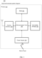
- FIG. 1 illustrates a high level system (system) 100 .
- the system will include a product 110 that can be input or output.
- the system 100 also includes a communication (comms) interface 120 that is configured to communicate with a microprocessor core 140 .
- the microprocessor core 140 will be powered by a power supply 130 that provides the main power, and include one or more processors.
- a nonvolatile storage 150 will be connected to the microprocessor 140.
- Random access memory (RAM) 160 is also illustrated.
- the RAM 160 is connected to the microprocessor core 140.
- the system 100 will receive input such as an inputted compressed image.
- the microprocessor core 140 will attempt to place any input within the system 100 into either the RAM 160 or the nonvolatile storage 150 .
- the nonvolatile storage 150 can be the arbitrary storage in which output and input can be redirected to if the RAM 160 does not have any available space to store the input and output.
- the input can also include an inputted compressed image.
- the microprocessor core 140 will make calls to a system of caches within the nonvolatile storage 150 to facilitate redirecting the input and output to the nonvolatile storage 150 due to the lack of available storage within the RAM 160.
- the microprocessor 140 will make the calls to the system of caches due to a shortage of memory in the RAM 160 , such as during a decompression process.
- the nonvolatile storage 150 can be within the same computing system as the microprocessor core 140 . Alternatively, the nonvolatile storage 150 can be external to the high-level system 100 as well.
- the microprocessor core 140 based on the calls to the system of caches, can redirect input and output to the nonvolatile storage 150 to store the input and output.
- the nonvolatile storage can include additional RAM, EEPROM, ROM, Flash, and other serial devices, etc.
- the microprocessor core 140 will make calls to a system of caches including the nonvolatile storage 150 to facilitate the redirection of the input and output.
- the microprocessor core 140 after making the calls to the system of caches, will then redirect the input and output to the nonvolatile storage 150 to allow the input and output to be stored within the nonvolatile storage 150 .
- the redirecting input and output can be stored in additional RAM, ROM, EEPROM, flash and/or one or more other serial devices.
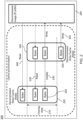
- FIG. 2 a system 200 with internal cache synchronization, wherein synchronization is needed only in case of overlap.
- the system 200 includes an overlap area 210 , a decompressed read cache RAM 220 , and a decompressed write cache RAM 245 .
- the decompressed read cache RAM 220 includes a plurality of data bytes 225 .
- the decompressed write cache RAM 245 will include data bytes 250 that are read into the decompressed read cache RAM 220 .
- the overlap area 210 is the area in which the decompressed read cache RAM 220 and the decompressed write cache RAM 245 overlap, and in which data bytes 250 from the decompressed write cache RAM 245 are read 235 and updated 230 into the decompressed read cache (RAM) 220 .
- the overlap area 210 would exist only if an intersection of buffers is not empty.
- a decompressed image flash 260 is also illustrated.
- the decompressed write cache RAM 245 will write 255 the data bytes 250 into the decompressed image flash 260 for storage.
- the decompressed write cache (RAM) 245 will write the data bytes 250 into the decompressed image flash 260 for storage.
- the microprocessor core will make calls to the system of memory caches that will include the decompressed image flash 260 to facilitate the redirecting of the data bytes 250 due to a lack of available storage in the decompressed read cache (RAM) 220 and the decompressed write cache (RAM) 245 .
- the decompressed image flash 260 will provide the arbitrary storage when the data bytes 225 , 250 cannot be stored in either the decompressed read cache RAM 220 or the decompressed write cache (RAM) 245 .
- the decompressed image flash 260 can be within the same system 200 as the decompressed read cache (RAM) 220 and the decompressed write cache (RAM) 245 , or external to the decompressed read cache (RAM) 220 and the decompressed write cache (RAM) 245 .
- the decompressed image flash 260 can also read 240 the data bytes 225 from the decompressed read cache RAM 220 .
- other arbitrary storage can be included such as ROM or EEPROM or additional RAM.
- One or more serial devices can be connected to the decompressed image flash 260 and other arbitrary storage including additional RAM, ROM, and EEPROM.
- data bytes 250 can be redirected into arbitrary storage such as the decompressed image flash 260 when storage is not available in either the decompressed write cache RAM 245 or the decompressed read cache RAM 220 .
- the microprocessor core will include a processor that will perform calls to arbitrary storage including the decompressed image flash 260 to facilitate for the data bytes 250 to be redirected to the decompressed image flash 260 and other arbitrary storage when storage is not available within internal cache synchronization within the decompressed read cache (RAM) 220 or decompressed write cache (RAM) 245 .
- the microprocessor core within the system 200 will make calls to a system of caches that include the decompressed image flash 260 to facilitate the data bytes 250 to be redirected when there is a lack of shortage.
- the microprocessor core using the decompressed write cache (RAM) 245 , will write 255 the data bytes 250 to the decompressed image flash 260 .
- the decompressed image flash 260 can be part of the same system 200 as the cache synchronization, or be external to the system 200 that includes the decompressed write cache (RAM) 245 .
- a system 300 in which decryption, decompression and reencryption occurs in parallel processes.
- the system 300 includes a manufacturer premises 305 and an external flash 308 as part of a manufacturer device.
- a plain text image 310 is compressed and becomes a plain text compressed image 320 .
- a manufacturer key 330 will encrypt the plain text compressed image 320 .
- the ciphered compressed image 5 will pass over the air download 335 and into the external flash 308 within the manufacturer device.
- a manufacturer key 340 will decrypt the ciphered compressed image 325 to enable the ciphered compressed image 5 to then be decompressed.
- the plain text compressed block 345 will then become decompressed and then become the plain text box 350 after decompression.
- the plain text box 350 can thereby be reencrypted. In other words, following the decryption and the decompression, the reencryption process can occur.
- the manufacturer or another key 355 can reencrypt the plain text box 350 .
- the plain text box 350 can become the ciphered image 6 after being reencrypted.
- a plain text image 310 is compressed and becomes a plain text compressed image 320 .
- the plain text compressed image 320 then goes thru a process of becoming encrypted, and then passes onto an external flash 308 to be decrypted, decompressed, and then reencrypted.
- the process of decryption, decompression, and reencryption all occur in parallel within the manufacture device or external flash 308 . Accordingly, within the external flash 308 , decryption, decompression, and reencryption can successfully occur in parallel for the ciphered compressed image .
- FIG. 4 a system 400 in which the parallel processes of decryption, decompression, and reencryption are illustrated.
- An inputted compressed image becomes an encrypted compressed image IMG 410 .
- a manufacturer key will encrypt the inputted compressed image to put forth the encrypted compressed IMG 410 .
- the encrypted compressed IMG 410 is passed onto a manufacturer device that includes a flash device. The decryption process can begin.
- the encrypted compressed image IMG 410 can then be decrypted.
- a manufacturer key within the manufacturer device can decrypt the encrypted compressed image 410.
- the inputted compressed IMG 410 is decrypted, it can become a decrypted compressed IMG 440 within the RAM 450 .
- the decompression process can begin. Moreover, the image can then become decompressed and become the decompressed IMG 430 . After decompression, the decompressed IMG can become encrypted again or reencrypted. A manufacturer or another key with the manufacturer device can reencrypt the decompressed IMG 430 . When the decompressed IMG 430 is reencrypted, the image can become the encrypted decompressed IMG 420 .
- the inputted and encrypted compressed IMG 410 is passed through the manufacturer device. Further, a manufacturer key can decrypt the encrypted compressed IMG 410 to produce the decrypted compressed IMG 440. After the decryption has occurred, the decrypted compressed IMG 440 can be decompressed. As such, after decompression, the decompressed IMG 430 is produced. After decompression, reencryption can occur. A manufacturer key can reencrypt the decompressed IMG 430 . After reencryption, the encrypted decompressed IMG 420 is produced. Overall, the decryption, decompression, and reencryption process all occur in parallel within the manufacturer device.
- FIG. 5 a process 500 of redirecting input and output due to a lack of storage is illustrated.
- RAM or other storage within a computing device or system lacks available space
- input and output can be redirected to nonvolatile storage.
- the nonvolatile storage can be external to the computing device or system, or be within the computing device or system.
- an inputted compressed image is received into a computing device or system.
- the process 500 can begin after the inputted compressed image is received.
- a designer using a microprocessor core, or a processor, can identify if there is a shortage of space within the computing device or system to store input and output including the inputted compressed image.
- the microprocessor core will perform calls to a system of memory caches to read and write the input and output.
- the microprocessor makes the calls to the system of memory caches to facilitate the redirecting of the input and output due to the lack of available storage space in the RAM within the computing system.
- microprocessor core will redirect the input and output to identified arbitrary storage.
- the arbitrary storage can be nonvolatile storage that can be within the same computing system as the computing device, or can be external to the computing device.
- the arbitrary storage can include additional RAM, or ROM, flash, and EEPROM.
- the arbitrary storage can include other serial devices. The input and output is thereby redirected to additional RAM, ROM, EEPROM, or flash for storage.
- a microprocessor core in a computing system can identify when there is a shortage of storage space within the storage of the computing system.
- the available RAM within the computing system may not have enough storage space to store input and output.
- the microprocessor core will make calls to a system of memory caches to attempt to redirect the input and output to one or more of the memory caches.
- the system of memory caches can be nonvolatile storage that can be within the computing system, or external to the computing system.
- the nonvolatile storage can include RAM, ROM EEPROM, Flash, and other serial device.
- the microprocessor core performs the calls to facilitate the redirecting of the input and output to the nonvolatile storage due to the lack of available storage.
- the nonvolatile storage can include any one of additional RAM, ROM EEPROM, flash, and other serial devices.
- the microprocessor core attempts to facilitate the redirecting of input and output when the microprocessor identifies a shortage of storage space within the computing system.
- the microprocessor core can redirect any input and output to the nonvolatile storage for storage due to a lack of available storage within the computing system.
- the nonvolatile storage can be within the same computing system, or can be external to the computing system.
- the nonvolatile storage can include additional RAM, and also ROM, EEPROM, flash, and other serial devices to store the redirected input and output.
- the decryption, decompression, and reencryption processes can be performed in parallel.
- An inputted compressed image can be decrypted by a manufacturer key within a manufacturer device. After it is decrypted, the decrypted compressed image can be decompressed into a plain text box. After decompression, the plain text box can be reencrypted into an encrypted decompressed image. Accordingly, the decryption, decompression, and reencryption processes are performed in parallel within the manufacturer device that includes one or more flash devices.
Landscapes
- Engineering & Computer Science (AREA)
- Theoretical Computer Science (AREA)
- Physics & Mathematics (AREA)
- General Engineering & Computer Science (AREA)
- General Physics & Mathematics (AREA)
- Computer Security & Cryptography (AREA)
- Software Systems (AREA)
- Computer Hardware Design (AREA)
- Memory System Of A Hierarchy Structure (AREA)
- Storage Device Security (AREA)
- Image Input (AREA)
- Stored Programmes (AREA)
Abstract
Description
- The present disclosure generally relates to redirecting input and output to arbitrary storage to enhance LZO compression and performing decryption, decompression, and reencryption in parallel processes.
- Firmware upgrade on embedded systems can be slow depending on communication speed and image size. Embedded systems also have limited processing and storage resources. Conventional art typically only works on RAM and is not usable as in embedded environments due to limited RAM space.
- In embedded systems, when there is a lack of storage space, there can be difficulty in finding storage space for additional input and output. Additional input can include one or more inputted compressed images.
- In addition, when firmware images are transferred to an embedded device, it will usually stored temporarily in external storage. Image encryption can be used to secure the image. If the image is compressed, it is necessary to decrypt the entire image before decompression. Moreover, the image then exits even for a short period as plaintext in its compressed or decompressed form.
- As such, a need exists to redirect input and output to arbitrary storage when there is a lack of storage space in the computing device or system. Additional storage is needed to redirect the input and output when there is a lack of storage available in the RAM within the computing device or system.
- Further, a need also exits to perform decryption, decompression and reencryption in parallel. In addition, a need exits to perform decryption, decompression, and reencryption in parallel without allowing an attacker to read, analyze, or use the image involved.
- The following summary is provided to facilitate an understanding of some of the features of the disclosed embodiments and is not intended to be a full description. A full appreciation of the various aspects of the embodiments disclosed herein can be gained by taking the specification, claims, drawings, and abstract as a whole.
- The aforementioned aspects and other objectives can now be achieved as described herein.
- In an embodiment, a method includes inputting a compressed image in a computing device. The method also includes performing calls to a system of memory caches to read and write input and output due to a shortage of memory that includes the inputted compressed image by the processor to facilitate a redirecting of the input and output due to the shortage of the memory during a decompression process. The method also includes redirecting the input and output by the processor to arbitrary storage.
- The method also includes redirecting the input and the output to one or more serial devices.
- The arbitrary storage includes additional RAM
- In an embodiment, a method includes receiving an inputted compressed image in one or more computing devices. The method also includes attempting to store the inputted compressed image by at least one processor, wherein the at least one processor performs calls to a system of memory caches due to a lack of available storage. Arbitrary storage with at least one of a random access memory (RAM) or Flash memory is selected to redirect additional input and output and the compressed image by the at least one processor. The method also includes sending the compressed image and additional input and output by the processor to the at least one of the RAM or Flash memory.
- The method further includes selecting a read-only memory for additional storage.
- The method further includes performing decryption and decompression in parallel without storing plaintext in non-volatile storage.
- In an embodiment, a system includes a computing device receiving an inputted compressed image. The method also includes a processor that performs calls to a system of memory caches to read and write input and output that includes the inputted compressed image to facilitate a redirecting of the input and output due to a shortage of the memory during a decompression process. The system also includes one or more serial devices including at least one read-only memory or at least one flash memory that receives the redirected input or output.
- The arbitrary storage includes an electrically erasable programmable read-only memory (EEPROM).
- The processor combines decryption and decompression in parallel processes.
- The accompanying figures, in which like reference numerals refer to identical or functionally similar elements throughout the separate views and which are incorporated and form a part of the specification, further illustrate the present invention and, together with the detailed description of the invention, serve to explain the principles of the present invention.
-
FIG. 1 illustrates a system diagram in accordance with an embodiment of the invention; -
FIG. 2 illustrates schematic diagram in accordance with an embodiment of the invention; -
FIG. 3 illustrates a system diagram in accordance with an embodiment of the invention; and -
FIG. 4 illustrates a system diagram in accordance with an embodiment of the invention. -
FIG. 5 depicts a flow chart in accordance with an embodiment of the invention. - Unless otherwise indicated illustrations in the figures are not necessarily drawn to scale.
- The particular values and configurations discussed in these nonlimiting examples can be varied and are cited merely to illustrate one or more embodiments and are not intended to limit the scope thereof.
- Subject matter will now be described more fully herein after with reference to the accompanying drawings, which form a part hereof, and which show, by way of illustration, specific example embodiments. Subject matter may, however, be embodied in a variety of different form and, therefore, covered or claimed subject matter is intended to be construed as not being limited to any example embodiments set forth herein, example embodiments are provided merely to be illustrative. Likewise, a reasonably broad scope for claimed or covered subject matter is intended. Among other issues, subject matter may be embodied as methods, devices, components, or systems. The followed detailed description is, therefore, not intended to be interpreted in a limiting sense.
- Throughout the specification and claims, terms may have nuanced meanings suggested or implied in context beyond an explicitly stated meaning. Likewise, phrases such as "in one embodiment" or "in an example embodiment" and variations thereof as utilized herein may not necessarily refer to the same embodiment and the phrase "in another embodiment" or "in another example embodiment" and variations thereof as utilized herein may or may not necessarily refer to a different embodiment. It is intended, for example, that claimed subject matter include combinations of example embodiments in whole or in part.
- In general, terminology may be understood, at least in part, from usage in context. For example, terms such as "and," "or," or "and/or" as used herein may include a variety of meanings that may depend, at least in part, upon the context in which such terms are used. Generally, "or" if used to associate a list, such as A, B, or C, is intended to mean A, B, and C, here used in the inclusive sense, as well as A, B, or C, here used in the exclusive sense. In addition, the term "one or more" as used herein, depending at least in part upon context, may be used to describe any feature, structure, or characteristic in a singular sense or may be used to describe combinations of features, structures, or characteristics in a plural sense. Similarly, terms such as a "a," "an," or "the", again, may be understood to convey a singular usage or to convey a plural usage, depending at least in part upon context. In addition, the term "based on" may be understood as not necessarily intended to convey an exclusive set of factors and may, instead, allow for existence of additional factors not necessarily expressly described, again, depending at least in part on context.
- One having ordinary skill in the relevant art will readily recognize the subject matter disclosed herein can be practiced without one or more of the specific details or with other methods. In other instances, well-known structures or operations are not shown in detail to avoid obscuring certain aspects. This disclosure is not limited by the illustrated ordering of acts or events, as some acts may occur in different orders and/or concurrently with other acts or events. Furthermore, not all illustrated acts or events are required to implement a methodology in accordance with the embodiments disclosed herein.
- Unless defined otherwise, all technical and scientific terms used herein have the same meanings as commonly understood by one of ordinary skill in the art to which the disclosed embodiments belong. Preferred methods, techniques, devices, and materials are described, although any methods, techniques, devices, or materials similar or equivalent to those described herein may be used in the practice or testing of the present invention.
- Although claims have been included in this application to specific enumerated combinations of features, it should be understood the scope of the present disclosure also includes any novel feature or any novel combination of features disclosed herein.
- References "an embodiment," "example embodiment," "various embodiments," "some embodiments," etc., may indicate that the embodiment(s) so described may include a particular feature, structure, or characteristic, but not every possible embodiment necessarily includes that particular feature, structure, or characteristic.
- Headings provided are for convenience and are not to be taken as limiting the present disclosure in any way.
- Each term utilized herein is to be given its broadest interpretation given the context in which that term is utilized.
- The following paragraphs provide context for terms found in the present disclosure (including the claims):
- The transitional term "comprising", which is synonymous with "including," "containing," or "characterized by," is inclusive or open-ended and does not exclude additional, unrecited elements or method steps. See, e.g., Mars Inc. v. H.J. Heinz Co., 377 F.3d 1369, 1376, 71 USPQ2d 1837, 1843 (Fed. Cir. 2004) ("[L]ike the term 'comprising,' the terms 'containing' and 'mixture' are open-ended."). "Configured to" or "operable for" is used to connote structure by indicating that the mechanisms/units/components include structure that performs the task or tasks during operation. "Configured to" may include adapting a manufacturing process to fabricate components that are adapted to implement or perform one or more tasks.
- "Based On." As used herein, this term is used to describe factors that affect a determination without otherwise precluding other or additional factors that may affect that determination. More particularly, such a determination may be solely "based on" those factors or based, at least in part, on those factors.
- All terms of example language (e.g., including, without limitation, "such as", "like", "for example", "for instance", "similar to", etc.) are not exclusive of other examples and therefore mean "by way of example, and not limitation..."
- A description of an embodiment having components in communication with each other does not infer that all enumerated components are needed.
- A commercial implementation in accordance with the scope and spirit of the present disclosure may be configured according to the needs of the particular application, whereby any function of the teachings related to any described embodiment of the present invention may be suitably changed by those skilled in the art.
- The flowchart and block diagrams in the figures illustrate the architecture, functionality, and operation of possible implementations of systems and methods according to various embodiments. Functions noted in the block may occur out of the order noted in the figures. For example, two blocks shown in succession may, in fact, be executed substantially concurrently, or the blocks may sometimes be executed in the reverse order, depending upon the functionality involved.
- Further, any sequence of steps that may be described does not necessarily indicate a condition that the steps be performed in that order. Some steps may be performed simultaneously.
- The functionality and/or the features of a particular component may be alternatively embodied by one or more other devices that are not explicitly described as having such functionality/features. Also, various embodiments of the present invention need not include a device itself.
- More specifically, as will be appreciated by one skilled in the art, aspects of the present invention may be embodied as a system and/or method. Furthermore, aspects of the present invention may take the form of a plurality of systems to enable gas meter to perform self-checking to determine its overall functioning without requiring a meter operator.
- Embodiments of the present invention include a computing system that lacks storage space in its internal random-access memory (RAM) and needs to be able to redirect input and output to arbitrary storage. The arbitrary storage can include nonvolatile storage that is located within the same computing system, or located externally to the computing system.
- In anticipation of the need to redirect input and output within the computing system to the arbitrary storage, a microprocessor core will perform calls to a system of memory caches to facilitate the redirecting of the input and output to the arbitrary storage.
- The arbitrary storage can include, but is not limited to, additional random-RAM, read-only memory (ROM), electrically erasable programmable read-only memory (EEPROM), flash, and one or more other serial devices. The microprocessor core can redirect the input and output to the nonvolatile or arbitrary storage in response to a lack of available storage within its internal RAM
- Embodiments of the present invention also include perform the process of decryption, decompression, and reencryption in parallel. The processes are perform in parallel to mitigate security risks by firmware images, such as when an attacker tries to read, analyze or otherwise use the image.
- In a manufacturer device, a manufacturer key will decrypt a compressed image. The image will then become decompressed and become a plain text box. Once it has become a plain text box, the plain text box can then be reencrypted. As such, the plain text box is reencrypted into a ciphered image. Accordingly, the decryption, decompression, and reencryption occur in parallel to mitigate the security risk presented by firmware images that are stored in plaintext.
-
FIG. 1 illustrates a high level system (system) 100. The system will include aproduct 110 that can be input or output. Thesystem 100 also includes a communication (comms)interface 120 that is configured to communicate with amicroprocessor core 140. Themicroprocessor core 140 will be powered by apower supply 130 that provides the main power, and include one or more processors. Anonvolatile storage 150 will be connected to themicroprocessor 140. Random access memory (RAM) 160 is also illustrated. TheRAM 160 is connected to themicroprocessor core 140. - Referring to
FIG. 1 , thesystem 100 will receive input such as an inputted compressed image. Themicroprocessor core 140 will attempt to place any input within thesystem 100 into either theRAM 160 or thenonvolatile storage 150. Thenonvolatile storage 150 can be the arbitrary storage in which output and input can be redirected to if theRAM 160 does not have any available space to store the input and output. The input can also include an inputted compressed image. Themicroprocessor core 140 will make calls to a system of caches within thenonvolatile storage 150 to facilitate redirecting the input and output to thenonvolatile storage 150 due to the lack of available storage within theRAM 160. Themicroprocessor 140 will make the calls to the system of caches due to a shortage of memory in theRAM 160, such as during a decompression process. Thenonvolatile storage 150 can be within the same computing system as themicroprocessor core 140. Alternatively, thenonvolatile storage 150 can be external to the high-level system 100 as well. - In
FIG. 1 , themicroprocessor core 140, based on the calls to the system of caches, can redirect input and output to thenonvolatile storage 150 to store the input and output. The nonvolatile storage can include additional RAM, EEPROM, ROM, Flash, and other serial devices, etc. When there is a lack of available space in theRAM 160 in the high-level system 100, themicroprocessor core 140 will make calls to a system of caches including thenonvolatile storage 150 to facilitate the redirection of the input and output. Themicroprocessor core 140, after making the calls to the system of caches, will then redirect the input and output to thenonvolatile storage 150 to allow the input and output to be stored within thenonvolatile storage 150. As such, the redirecting input and output can be stored in additional RAM, ROM, EEPROM, flash and/or one or more other serial devices. - In
FIG. 2 , asystem 200 with internal cache synchronization, wherein synchronization is needed only in case of overlap. A process in which output and input is redirected to arbitrary storage in further detail is shown. Thesystem 200 includes anoverlap area 210, a decompressedread cache RAM 220, and a decompressedwrite cache RAM 245. The decompressedread cache RAM 220 includes a plurality ofdata bytes 225. The decompressedwrite cache RAM 245 will includedata bytes 250 that are read into the decompressedread cache RAM 220. Theoverlap area 210 is the area in which the decompressedread cache RAM 220 and the decompressedwrite cache RAM 245 overlap, and in whichdata bytes 250 from the decompressedwrite cache RAM 245 are read 235 and updated 230 into the decompressed read cache (RAM) 220. Theoverlap area 210 would exist only if an intersection of buffers is not empty. - Referring to
FIG. 2 , a decompressedimage flash 260 is also illustrated. The decompressedwrite cache RAM 245 will write 255 thedata bytes 250 into the decompressedimage flash 260 for storage. When storage is not available in the decompressedwrite cache RAM 245 or the decompressedread cache RAM 220, the decompressed write cache (RAM) 245 will write thedata bytes 250 into the decompressedimage flash 260 for storage. The microprocessor core will make calls to the system of memory caches that will include the decompressedimage flash 260 to facilitate the redirecting of thedata bytes 250 due to a lack of available storage in the decompressed read cache (RAM) 220 and the decompressed write cache (RAM) 245. The decompressedimage flash 260 will provide the arbitrary storage when thedata bytes read cache RAM 220 or the decompressed write cache (RAM) 245. The decompressedimage flash 260 can be within thesame system 200 as the decompressed read cache (RAM) 220 and the decompressed write cache (RAM) 245, or external to the decompressed read cache (RAM) 220 and the decompressed write cache (RAM) 245. The decompressedimage flash 260 can also read 240 thedata bytes 225 from the decompressedread cache RAM 220. Although the decompressedimage flash 260 is illustrated, other arbitrary storage can be included such as ROM or EEPROM or additional RAM. One or more serial devices can be connected to the decompressedimage flash 260 and other arbitrary storage including additional RAM, ROM, and EEPROM. - In
FIG. 2 , in summary,data bytes 250 can be redirected into arbitrary storage such as the decompressedimage flash 260 when storage is not available in either the decompressedwrite cache RAM 245 or the decompressedread cache RAM 220. The microprocessor core will include a processor that will perform calls to arbitrary storage including the decompressedimage flash 260 to facilitate for thedata bytes 250 to be redirected to the decompressedimage flash 260 and other arbitrary storage when storage is not available within internal cache synchronization within the decompressed read cache (RAM) 220 or decompressed write cache (RAM) 245. As such, when there is no available storage within thesystem 200, the microprocessor core within thesystem 200 will make calls to a system of caches that include the decompressedimage flash 260 to facilitate thedata bytes 250 to be redirected when there is a lack of shortage. Ultimately, the microprocessor core, using the decompressed write cache (RAM) 245, will write 255 thedata bytes 250 to the decompressedimage flash 260. The decompressedimage flash 260 can be part of thesame system 200 as the cache synchronization, or be external to thesystem 200 that includes the decompressed write cache (RAM) 245. In addition, although not represented inFIG. 2 , there is a third cache that is used only for reading data from a compressed image. - In
FIG. 3 , asystem 300 in which decryption, decompression and reencryption occurs in parallel processes. Thesystem 300 includes amanufacturer premises 305 and anexternal flash 308 as part of a manufacturer device. A plain text image 310 is compressed and becomes a plain text compressedimage 320. Amanufacturer key 330 will encrypt the plain text compressedimage 320. The ciphered compressed image 5 will pass over theair download 335 and into theexternal flash 308 within the manufacturer device. - With respect to
FIG. 3 , amanufacturer key 340 will decrypt the cipheredcompressed image 325 to enable the ciphered compressed image 5 to then be decompressed. When the ciphered compressed image 5 is decrypted, it will become the plain text compressedblock 345. The plain text compressed block 345 will then become decompressed and then become theplain text box 350 after decompression. Further, after the plain text compressedblock 345 is decompressed, and has become theplain text box 350, theplain text box 350 can thereby be reencrypted. In other words, following the decryption and the decompression, the reencryption process can occur. The manufacturer or another key 355 can reencrypt theplain text box 350. Theplain text box 350 can become the ciphered image 6 after being reencrypted. - Referring to
FIG. 3 , in summary, a plain text image 310 is compressed and becomes a plain text compressedimage 320. The plain text compressedimage 320 then goes thru a process of becoming encrypted, and then passes onto anexternal flash 308 to be decrypted, decompressed, and then reencrypted. The process of decryption, decompression, and reencryption all occur in parallel within the manufacture device orexternal flash 308. Accordingly, within theexternal flash 308, decryption, decompression, and reencryption can successfully occur in parallel for the ciphered compressed image . - In
FIG. 4 , asystem 400 in which the parallel processes of decryption, decompression, and reencryption are illustrated. An inputted compressed image becomes an encryptedcompressed image IMG 410. Moreover, a manufacturer key will encrypt the inputted compressed image to put forth the encryptedcompressed IMG 410. The encryptedcompressed IMG 410 is passed onto a manufacturer device that includes a flash device. The decryption process can begin. The encryptedcompressed image IMG 410 can then be decrypted. A manufacturer key within the manufacturer device can decrypt the encryptedcompressed image 410. When the inputtedcompressed IMG 410 is decrypted, it can become a decryptedcompressed IMG 440 within theRAM 450. After the image has been decrypted to be the decryptedcompressed IMG 440, the decompression process can begin. Moreover, the image can then become decompressed and become the decompressed IMG 430. After decompression, the decompressed IMG can become encrypted again or reencrypted. A manufacturer or another key with the manufacturer device can reencrypt the decompressed IMG 430. When the decompressed IMG 430 is reencrypted, the image can become the encrypted decompressedIMG 420. - Referring to
FIG. 4 , a parallel process of decryption, decompression and reencryption is illustrated. The inputted and encryptedcompressed IMG 410 is passed through the manufacturer device. Further, a manufacturer key can decrypt the encryptedcompressed IMG 410 to produce the decryptedcompressed IMG 440. After the decryption has occurred, the decryptedcompressed IMG 440 can be decompressed. As such, after decompression, the decompressed IMG 430 is produced. After decompression, reencryption can occur. A manufacturer key can reencrypt the decompressed IMG 430. After reencryption, the encrypted decompressedIMG 420 is produced. Overall, the decryption, decompression, and reencryption process all occur in parallel within the manufacturer device. - In
FIG. 5 , aprocess 500 of redirecting input and output due to a lack of storage is illustrated. When RAM or other storage within a computing device or system lacks available space, input and output can be redirected to nonvolatile storage. The nonvolatile storage can be external to the computing device or system, or be within the computing device or system. - In
FIG. 5 , atstep 510, at an initial step or state, an inputted compressed image is received into a computing device or system. Theprocess 500 can begin after the inputted compressed image is received. - Referring to
FIG. 5 , atstep 520, a designer, using a microprocessor core, or a processor, can identify if there is a shortage of space within the computing device or system to store input and output including the inputted compressed image. - In
FIG. 5 , atstep 530, the microprocessor core will perform calls to a system of memory caches to read and write the input and output. The microprocessor makes the calls to the system of memory caches to facilitate the redirecting of the input and output due to the lack of available storage space in the RAM within the computing system. - Referring to
FIG. 5 , atstep 540, microprocessor core will redirect the input and output to identified arbitrary storage. The arbitrary storage can be nonvolatile storage that can be within the same computing system as the computing device, or can be external to the computing device. The arbitrary storage can include additional RAM, or ROM, flash, and EEPROM. Moreover, the arbitrary storage can include other serial devices. The input and output is thereby redirected to additional RAM, ROM, EEPROM, or flash for storage. - Those skilled in the art will appreciate that the example embodiments are non-exhaustive and that embodiments other than that described here may be included without departing from the scope and spirit of the presently disclosed embodiments.
- Overall, a microprocessor core in a computing system can identify when there is a shortage of storage space within the storage of the computing system. The available RAM within the computing system may not have enough storage space to store input and output.
- In anticipation of having to redirect the input and output, the microprocessor core will make calls to a system of memory caches to attempt to redirect the input and output to one or more of the memory caches. Moreover, the system of memory caches can be nonvolatile storage that can be within the computing system, or external to the computing system. The nonvolatile storage can include RAM, ROM EEPROM, Flash, and other serial device. As such, the microprocessor core performs the calls to facilitate the redirecting of the input and output to the nonvolatile storage due to the lack of available storage.
- After performing the calls to the system of memory caches to facilitate the redirecting of the input and output to the nonvolatile storage, the microprocessor core redirects the input and output to the nonvolatile storage. The nonvolatile storage can include any one of additional RAM, ROM EEPROM, flash, and other serial devices.
- Accordingly, the microprocessor core attempts to facilitate the redirecting of input and output when the microprocessor identifies a shortage of storage space within the computing system. After the calls are made to the system of memory caches, the microprocessor core can redirect any input and output to the nonvolatile storage for storage due to a lack of available storage within the computing system. The nonvolatile storage can be within the same computing system, or can be external to the computing system. The nonvolatile storage can include additional RAM, and also ROM, EEPROM, flash, and other serial devices to store the redirected input and output.
- In addition, the decryption, decompression, and reencryption processes can be performed in parallel. An inputted compressed image can be decrypted by a manufacturer key within a manufacturer device. After it is decrypted, the decrypted compressed image can be decompressed into a plain text box. After decompression, the plain text box can be reencrypted into an encrypted decompressed image. Accordingly, the decryption, decompression, and reencryption processes are performed in parallel within the manufacturer device that includes one or more flash devices.
- All references, including granted patents and patent application publications, referred herein are incorporated herein by reference in their entirety.
- All the features disclosed in this specification, including any accompanying abstract and drawings, may be replaced by alternative features serving the same, equivalent or similar purpose, unless expressly stated otherwise. Thus, unless expressly stated otherwise, each feature disclosed is one example only of a generic series of equivalent or similar features.
- Various aspects of the invention have been described above by way of illustration, and the specific embodiments disclosed are not intended to limit the invention to the particular forms disclosed. The particular implementation of the system provided thereof may vary depending upon the particular context or application. The invention is thus to cover all modifications, equivalents, and alternatives falling within the spirit and scope of the following claims. It is to be further understood that not all of the disclosed embodiments in the foregoing specification will necessarily satisfy or achieve each of the objects, advantages, or improvements described in the foregoing specification.
- The corresponding structures, materials, acts, and equivalents of all means or step plus function elements in the claims below are intended to include any structure, material, or act for performing the function in combination with other claimed elements as specifically claimed.
Claims (10)
- A method comprising:inputting a compressed image (410) in a computing device (100);identifying a shortage of random access memory (RAM) (160) during a decompression process by processor (140), performing calls to a system of memory caches (150) to read and write input and output including the inputted compressed image (410) by the processor (140), and identifying arbitrary storage (150) to read and write the input and output by the processor (140); andredirecting the input and output by the processor (140) to the identified arbitrary storage (150).
- The method of claim 1, wherein the decompressed image (430) overrides the inputted compressed image (410) to complete the decompression process.
- The method of claim 1, wherein the arbitrary storage includes additional RAM (150).
- The method of claim 1, further comprising:
adding additional memory caches (150) to speed up decompression speed. - The method of claim 1, wherein the input and output are redirected to an electrically erasable programmable read-only memory (EEPROM) (150).
- The method of claim 1, wherein the input and output are redirected to serial devices (150).
- The method of claim 1, further comprising:
replacing all direct RAM (160) accesses in response to identifying the shortage of
RAM (160). - A method comprising:receiving an inputted compressed image (410) in one or more computing devices (100);attempting to store the inputted compressed image (410) by at least one processor (140), wherein the at least one processor (140) performs calls to a system of memory caches (150) due to a lack of available storage, and wherein arbitrary storage (150) with at least one of a random access memory (RAM) (150) or Flash memory (150) is located by the at least one processor (140); andsending the compressed image and additional input and output by the processor (140) to the at least one of the RAM (150) or Flash memory (150).
- The method of claim 1, further comprising:
identifying a read-only memory (150) for additional storage. - The method of claim 8, further comprising:
performing decryption and decompression in parallel without
storing plaintext in non-volatile storage (150).
Applications Claiming Priority (1)
| Application Number | Priority Date | Filing Date | Title |
|---|---|---|---|
| US17/456,969 US12450179B2 (en) | 2021-11-30 | 2021-11-30 | LZO decompression in external storage |
Publications (2)
| Publication Number | Publication Date |
|---|---|
| EP4198747A1 true EP4198747A1 (en) | 2023-06-21 |
| EP4198747B1 EP4198747B1 (en) | 2025-02-12 |
Family
ID=84370343
Family Applications (1)
| Application Number | Title | Priority Date | Filing Date |
|---|---|---|---|
| EP22210345.9A Active EP4198747B1 (en) | 2021-11-30 | 2022-11-29 | Lzo decompression in external storage |
Country Status (5)
| Country | Link |
|---|---|
| US (1) | US12450179B2 (en) |
| EP (1) | EP4198747B1 (en) |
| KR (1) | KR20230081684A (en) |
| CA (1) | CA3183469A1 (en) |
| MX (1) | MX2022015131A (en) |
Families Citing this family (4)
| Publication number | Priority date | Publication date | Assignee | Title |
|---|---|---|---|---|
| US12112199B2 (en) | 2021-11-30 | 2024-10-08 | Honeywell International Inc. | Interruptible LZO decompression |
| US12450179B2 (en) * | 2021-11-30 | 2025-10-21 | Honeywell International Inc. | LZO decompression in external storage |
| US12124839B2 (en) | 2021-12-27 | 2024-10-22 | Honeywell International Inc. | BSIDIFF delta upgrade in external storage |
| US12079622B2 (en) | 2022-01-05 | 2024-09-03 | Honeywell International Inc. | Interruptable BSDIFF delta decompression |
Citations (3)
| Publication number | Priority date | Publication date | Assignee | Title |
|---|---|---|---|---|
| JP2003216465A (en) * | 2002-01-21 | 2003-07-31 | Seiko Epson Corp | Display device and cache control method for display device |
| US6636958B2 (en) * | 2001-07-17 | 2003-10-21 | International Business Machines Corporation | Appliance server with a drive partitioning scheme that accommodates application growth in size |
| US20180095668A1 (en) * | 2015-02-13 | 2018-04-05 | Google Llc | Transparent Hardware-Assisted Memory Decompression |
Family Cites Families (68)
| Publication number | Priority date | Publication date | Assignee | Title |
|---|---|---|---|---|
| US5255378A (en) * | 1989-04-05 | 1993-10-19 | Intel Corporation | Method of transferring burst data in a microprocessor |
| US5835740A (en) * | 1992-06-30 | 1998-11-10 | Discovision Associates | Data pipeline system and data encoding method |
| US5359676A (en) | 1993-07-19 | 1994-10-25 | Xerox Corporation | Decompression of standard ADCT-compressed document images |
| US6081752A (en) | 1995-06-07 | 2000-06-27 | International Business Machines Corporation | Computer system having power supply primary sense to facilitate performance of tasks at power off |
| US5890014A (en) * | 1996-08-05 | 1999-03-30 | Micronet Technology, Inc. | System for transparently identifying and matching an input/output profile to optimal input/output device parameters |
| US20030182414A1 (en) | 2003-05-13 | 2003-09-25 | O'neill Patrick J. | System and method for updating and distributing information |
| US7328007B2 (en) | 2001-07-26 | 2008-02-05 | Kyocera Wireless Corp. | System and method for organizing wireless communication device system software |
| US7478235B2 (en) * | 2002-06-28 | 2009-01-13 | Microsoft Corporation | Methods and systems for protecting data in USB systems |
| US7111142B2 (en) | 2002-09-13 | 2006-09-19 | Seagate Technology Llc | System for quickly transferring data |
| US7886093B1 (en) | 2003-07-31 | 2011-02-08 | Hewlett-Packard Development Company, L.P. | Electronic device network supporting compression and decompression in electronic devices |
| KR100880783B1 (en) | 2003-09-03 | 2009-02-02 | 휴렛-팩커드 디벨롭먼트 컴퍼니, 엘 피 | 3-step boot process on electronics |
| US7734932B2 (en) * | 2003-11-10 | 2010-06-08 | Broadcom Corporation | System and method for securing executable code |
| US7657533B2 (en) | 2003-11-26 | 2010-02-02 | Hewlett-Packard Development Company, L.P. | Data management systems, data management system storage devices, articles of manufacture, and data management methods |
| US7549042B2 (en) | 2003-12-16 | 2009-06-16 | Microsoft Corporation | Applying custom software image updates to non-volatile storage in a failsafe manner |
| US7657706B2 (en) * | 2003-12-18 | 2010-02-02 | Cisco Technology, Inc. | High speed memory and input/output processor subsystem for efficiently allocating and using high-speed memory and slower-speed memory |
| US7512750B2 (en) * | 2003-12-31 | 2009-03-31 | Intel Corporation | Processor and memory controller capable of use in computing system that employs compressed cache lines' worth of information |
| US7761863B2 (en) | 2004-06-08 | 2010-07-20 | Covia Labs, Inc. | Method system and data structure for content renditioning adaptation and interoperability segmentation model |
| US8135958B2 (en) | 2005-11-22 | 2012-03-13 | International Business Machines Corporation | Method, system, and apparatus for dynamically validating a data encryption operation |
| ATE491988T1 (en) | 2005-12-20 | 2011-01-15 | Ericsson Telefon Ab L M | CREATING INCREMENTAL PROGRAM UPDATES |
| US8055096B2 (en) | 2006-05-10 | 2011-11-08 | Research In Motion Limited | Method and system for incremental patching of binary files |
| US7779401B2 (en) | 2006-06-26 | 2010-08-17 | Research In Motion Limited | Method and system for generating a reverse binary patch for undoing a software update |
| US8341604B2 (en) | 2006-11-15 | 2012-12-25 | Qualcomm Incorporated | Embedded trace macrocell for enhanced digital signal processor debugging operations |
| WO2008078390A1 (en) | 2006-12-26 | 2008-07-03 | Fujitsu Limited | Data compression device and data restoring device |
| KR100842680B1 (en) * | 2007-01-08 | 2008-07-01 | 삼성전자주식회사 | Error Correction Controller of Flash Memory Device and Memory System Including It |
| JP4944686B2 (en) | 2007-06-28 | 2012-06-06 | ソニーモバイルコミュニケーションズ株式会社 | Software update method and portable terminal device |
| US8175418B1 (en) | 2007-10-26 | 2012-05-08 | Maxsp Corporation | Method of and system for enhanced data storage |
| US9720616B2 (en) | 2008-06-18 | 2017-08-01 | Super Talent Technology, Corp. | Data-retention controller/driver for stand-alone or hosted card reader, solid-state-drive (SSD), or super-enhanced-endurance SSD (SEED) |
| US8015220B1 (en) | 2008-08-05 | 2011-09-06 | Smith Micro Software, Inc. | Block-based differencing algorithm |
| JP5342302B2 (en) | 2009-03-30 | 2013-11-13 | 株式会社日立ソリューションズ | Firmware update system, firmware distribution server, and program |
| CN101930387A (en) | 2009-06-19 | 2010-12-29 | 上海惠普有限公司 | Improved fault tolerance method and device used for updating compressed read-only file system |
| GB201003962D0 (en) | 2010-03-10 | 2010-04-21 | Tangentix Ltd | Multimedia content delivery system |
| KR20120041384A (en) | 2010-10-21 | 2012-05-02 | 삼성전자주식회사 | Method and apparatus for updating firmware of mobile device |
| US20120150877A1 (en) | 2010-12-09 | 2012-06-14 | Microsoft Corporation | Efficient database compression |
| US20120227036A1 (en) | 2011-03-01 | 2012-09-06 | International Business Machines Corporation | Local Server Management of Software Updates to End Hosts Over Low Bandwidth, Low Throughput Channels |
| KR101717081B1 (en) * | 2011-03-23 | 2017-03-28 | 삼성전자주식회사 | Storage device comprising a buffer memory by using a nonvolatile-ram and volatile-ram |
| EP2761476B1 (en) | 2011-09-30 | 2017-10-25 | Intel Corporation | Apparatus, method and system that stores bios in non-volatile random access memory |
| EP3364304B1 (en) * | 2011-09-30 | 2022-06-15 | INTEL Corporation | Memory channel that supports near memory and far memory access |
| US9792439B2 (en) | 2012-09-19 | 2017-10-17 | Nxp B.V. | Method and system for securely updating firmware in a computing device |
| KR101541112B1 (en) | 2013-07-04 | 2015-07-31 | 주식회사 미르코퍼레이션 | FOTA system and the method |
| KR102262102B1 (en) * | 2014-04-09 | 2021-06-09 | 삼성전자 주식회사 | Method and apparatus for application execution |
| EP3303996A1 (en) | 2015-06-04 | 2018-04-11 | HERE Global B.V. | Incremental update of compressed navigational databases |
| KR102400384B1 (en) * | 2015-06-26 | 2022-05-23 | 삼성전자 주식회사 | Electronic device having an external memory and method operating the same |
| US20170048303A1 (en) | 2015-08-10 | 2017-02-16 | TransferSoft, Inc. | On the fly statistical delta differencing engine |
| JP6675271B2 (en) | 2015-09-14 | 2020-04-01 | パナソニック インテレクチュアル プロパティ コーポレーション オブ アメリカPanasonic Intellectual Property Corporation of America | Gateway device, in-vehicle network system, and firmware update method |
| US9946533B2 (en) | 2015-09-30 | 2018-04-17 | Apple Inc. | Software updating |
| US10887430B2 (en) | 2015-10-21 | 2021-01-05 | Dragonwave-X, Llc | Compression in communications |
| KR102547815B1 (en) * | 2015-12-30 | 2023-06-27 | 에스케이하이닉스 주식회사 | Electronic device and method for fabricating the same |
| US20170212750A1 (en) | 2016-01-22 | 2017-07-27 | Rigado, LLC | Compressed binary patching over wireless network |
| US10983704B1 (en) * | 2016-05-20 | 2021-04-20 | Emc Corporation | Method and system for adaptive wear leveling in solid state memory |
| US20170337204A1 (en) | 2016-05-23 | 2017-11-23 | TransferSoft, Inc. | Differencing engine for moving pictures |
| US20180060235A1 (en) | 2016-08-30 | 2018-03-01 | Intel Corporation | Non-volatile memory compression devices and associated methods and systems |
| WO2018091085A1 (en) | 2016-11-16 | 2018-05-24 | Huawei Technologies Co., Ltd. | Device and method for updating data on the device |
| WO2018134882A1 (en) * | 2017-01-17 | 2018-07-26 | オリンパス株式会社 | Memory access device, image processing apparatus, and imaging apparatus |
| US10757425B2 (en) | 2017-07-24 | 2020-08-25 | United States Postal Service | Image encryption through dynamic compression code words |
| WO2019042546A1 (en) | 2017-08-30 | 2019-03-07 | Huawei Technologies Co., Ltd. | Method for improving the robustness of in-place firmware update |
| WO2019077607A1 (en) | 2017-10-17 | 2019-04-25 | Argus Cyber Security Ltd. | System and method for managing program memory on a storage device |
| TW201923566A (en) | 2017-11-15 | 2019-06-16 | 財團法人工業技術研究院 | Systems and methods for updating vehicle electronic equipment |
| US10834207B2 (en) | 2018-02-27 | 2020-11-10 | Excelfore Corporation | System and method for updating software in an electronic device |
| US10796660B2 (en) | 2018-10-12 | 2020-10-06 | Samsung Display Co., Ltd. | Content adaptive display interface |
| EP3647944A1 (en) | 2018-10-30 | 2020-05-06 | Shenzhen Goodix Technology Co., Ltd. | Memory optimized block-based differential update algorithm |
| EP3680773B1 (en) | 2019-01-08 | 2023-08-02 | Argus Cyber Security Ltd | System and method for updating a computing device |
| JP6773984B2 (en) | 2019-01-30 | 2020-10-21 | 富士通クライアントコンピューティング株式会社 | Information processing equipment, methods and programs |
| EP3874365B1 (en) | 2019-10-31 | 2025-11-26 | Google LLC | Memory efficient software patching for updating applications on computing devices |
| US11175859B1 (en) * | 2020-07-14 | 2021-11-16 | Micron Technology, Inc. | Managing memory commands in a memory subsystem by adjusting a maximum number of low priority commands in a DRAM controller |
| US11886346B2 (en) * | 2021-04-22 | 2024-01-30 | Micron Technology, Inc. | Cache read context switching in a memory sub-system |
| US12450179B2 (en) * | 2021-11-30 | 2025-10-21 | Honeywell International Inc. | LZO decompression in external storage |
| US12112199B2 (en) | 2021-11-30 | 2024-10-08 | Honeywell International Inc. | Interruptible LZO decompression |
| US12124839B2 (en) | 2021-12-27 | 2024-10-22 | Honeywell International Inc. | BSIDIFF delta upgrade in external storage |
-
2021
- 2021-11-30 US US17/456,969 patent/US12450179B2/en active Active
-
2022
- 2022-11-29 MX MX2022015131A patent/MX2022015131A/en unknown
- 2022-11-29 EP EP22210345.9A patent/EP4198747B1/en active Active
- 2022-11-30 KR KR1020220164454A patent/KR20230081684A/en active Pending
- 2022-11-30 CA CA3183469A patent/CA3183469A1/en active Pending
Patent Citations (3)
| Publication number | Priority date | Publication date | Assignee | Title |
|---|---|---|---|---|
| US6636958B2 (en) * | 2001-07-17 | 2003-10-21 | International Business Machines Corporation | Appliance server with a drive partitioning scheme that accommodates application growth in size |
| JP2003216465A (en) * | 2002-01-21 | 2003-07-31 | Seiko Epson Corp | Display device and cache control method for display device |
| US20180095668A1 (en) * | 2015-02-13 | 2018-04-05 | Google Llc | Transparent Hardware-Assisted Memory Decompression |
Also Published As
| Publication number | Publication date |
|---|---|
| CA3183469A1 (en) | 2023-05-30 |
| KR20230081684A (en) | 2023-06-07 |
| MX2022015131A (en) | 2023-08-03 |
| US12450179B2 (en) | 2025-10-21 |
| US20230169020A1 (en) | 2023-06-01 |
| EP4198747B1 (en) | 2025-02-12 |
Similar Documents
| Publication | Publication Date | Title |
|---|---|---|
| US12450179B2 (en) | LZO decompression in external storage | |
| US8356188B2 (en) | Secure system-on-chip | |
| EP3690661B1 (en) | Flexible counter system for memory protection | |
| EP1341071A2 (en) | Memory card | |
| CN108959978A (en) | The generation of key and acquisition methods and device in equipment | |
| US20160357963A1 (en) | Protecting a secure boot process against side channel attacks | |
| CN110990186A (en) | System-on-chip, method of operating system-on-chip, and storage system | |
| WO2012177295A1 (en) | Requested and allowed cryptographic operations comparison | |
| US20120096257A1 (en) | Apparatus and Method for Protecting Storage Data of a Computing Apparatus in an Enterprise Network System | |
| KR101305627B1 (en) | Cryptographic apparatus and memory system | |
| CN111814162B (en) | A Kernel Sensitive Data Protection Method Based on Custom Hardware Security Attributes | |
| EP3271828B1 (en) | Cache and data organization for memory protection | |
| CN103488958A (en) | Manage the use of FPGAs with isolated components | |
| EP4148606B1 (en) | Data encryption or decryption method, apparatus and system | |
| US20210218545A1 (en) | Protecting cryptographic key data | |
| CN111241556A (en) | A data security storage method, device, storage medium and terminal | |
| US11121867B2 (en) | Encryption methods based on plaintext length | |
| KR102690536B1 (en) | Apparatus and method for encryption | |
| CN104392153B (en) | A kind of method for protecting software and system | |
| EP2940621B1 (en) | Apparatus, system, and method for controlling encryption and decryption with respect to a key | |
| CN106250783A (en) | A kind of database data encryption, decryption method and device | |
| US20180241547A1 (en) | System, apparatus, and method for securing data using a graphics processor | |
| US20070192624A1 (en) | Decryption processing apparatus, decryption method and image forming apparatus | |
| US9191211B2 (en) | Data security system | |
| US20090064317A1 (en) | Data protection system and method thereof |
Legal Events
| Date | Code | Title | Description |
|---|---|---|---|
| PUAI | Public reference made under article 153(3) epc to a published international application that has entered the european phase |
Free format text: ORIGINAL CODE: 0009012 |
|
| STAA | Information on the status of an ep patent application or granted ep patent |
Free format text: STATUS: REQUEST FOR EXAMINATION WAS MADE |
|
| 17P | Request for examination filed |
Effective date: 20221129 |
|
| AK | Designated contracting states |
Kind code of ref document: A1 Designated state(s): AL AT BE BG CH CY CZ DE DK EE ES FI FR GB GR HR HU IE IS IT LI LT LU LV MC ME MK MT NL NO PL PT RO RS SE SI SK SM TR |
|
| RIC1 | Information provided on ipc code assigned before grant |
Ipc: G06F 12/0868 20160101ALI20240821BHEP Ipc: G06F 12/06 20060101AFI20240821BHEP |
|
| GRAP | Despatch of communication of intention to grant a patent |
Free format text: ORIGINAL CODE: EPIDOSNIGR1 |
|
| STAA | Information on the status of an ep patent application or granted ep patent |
Free format text: STATUS: GRANT OF PATENT IS INTENDED |
|
| INTG | Intention to grant announced |
Effective date: 20241001 |
|
| GRAS | Grant fee paid |
Free format text: ORIGINAL CODE: EPIDOSNIGR3 |
|
| GRAA | (expected) grant |
Free format text: ORIGINAL CODE: 0009210 |
|
| STAA | Information on the status of an ep patent application or granted ep patent |
Free format text: STATUS: THE PATENT HAS BEEN GRANTED |
|
| AK | Designated contracting states |
Kind code of ref document: B1 Designated state(s): AL AT BE BG CH CY CZ DE DK EE ES FI FR GB GR HR HU IE IS IT LI LT LU LV MC ME MK MT NL NO PL PT RO RS SE SI SK SM TR |
|
| REG | Reference to a national code |
Ref country code: GB Ref legal event code: FG4D |
|
| REG | Reference to a national code |
Ref country code: CH Ref legal event code: EP |
|
| REG | Reference to a national code |
Ref country code: DE Ref legal event code: R096 Ref document number: 602022010456 Country of ref document: DE |
|
| REG | Reference to a national code |
Ref country code: IE Ref legal event code: FG4D |
|
| REG | Reference to a national code |
Ref country code: NL Ref legal event code: MP Effective date: 20250212 |
|
| PG25 | Lapsed in a contracting state [announced via postgrant information from national office to epo] |
Ref country code: RS Free format text: LAPSE BECAUSE OF FAILURE TO SUBMIT A TRANSLATION OF THE DESCRIPTION OR TO PAY THE FEE WITHIN THE PRESCRIBED TIME-LIMIT Effective date: 20250512 |
|
| PG25 | Lapsed in a contracting state [announced via postgrant information from national office to epo] |
Ref country code: FI Free format text: LAPSE BECAUSE OF FAILURE TO SUBMIT A TRANSLATION OF THE DESCRIPTION OR TO PAY THE FEE WITHIN THE PRESCRIBED TIME-LIMIT Effective date: 20250212 |
|
| PG25 | Lapsed in a contracting state [announced via postgrant information from national office to epo] |
Ref country code: PL Free format text: LAPSE BECAUSE OF FAILURE TO SUBMIT A TRANSLATION OF THE DESCRIPTION OR TO PAY THE FEE WITHIN THE PRESCRIBED TIME-LIMIT Effective date: 20250212 |
|
| PG25 | Lapsed in a contracting state [announced via postgrant information from national office to epo] |
Ref country code: ES Free format text: LAPSE BECAUSE OF FAILURE TO SUBMIT A TRANSLATION OF THE DESCRIPTION OR TO PAY THE FEE WITHIN THE PRESCRIBED TIME-LIMIT Effective date: 20250212 |
|
| REG | Reference to a national code |
Ref country code: LT Ref legal event code: MG9D |
|
| PG25 | Lapsed in a contracting state [announced via postgrant information from national office to epo] |
Ref country code: IS Free format text: LAPSE BECAUSE OF FAILURE TO SUBMIT A TRANSLATION OF THE DESCRIPTION OR TO PAY THE FEE WITHIN THE PRESCRIBED TIME-LIMIT Effective date: 20250612 Ref country code: NO Free format text: LAPSE BECAUSE OF FAILURE TO SUBMIT A TRANSLATION OF THE DESCRIPTION OR TO PAY THE FEE WITHIN THE PRESCRIBED TIME-LIMIT Effective date: 20250512 |
|
| PG25 | Lapsed in a contracting state [announced via postgrant information from national office to epo] |
Ref country code: NL Free format text: LAPSE BECAUSE OF FAILURE TO SUBMIT A TRANSLATION OF THE DESCRIPTION OR TO PAY THE FEE WITHIN THE PRESCRIBED TIME-LIMIT Effective date: 20250212 |
|
| PG25 | Lapsed in a contracting state [announced via postgrant information from national office to epo] |
Ref country code: HR Free format text: LAPSE BECAUSE OF FAILURE TO SUBMIT A TRANSLATION OF THE DESCRIPTION OR TO PAY THE FEE WITHIN THE PRESCRIBED TIME-LIMIT Effective date: 20250212 |
|
| PG25 | Lapsed in a contracting state [announced via postgrant information from national office to epo] |
Ref country code: PT Free format text: LAPSE BECAUSE OF FAILURE TO SUBMIT A TRANSLATION OF THE DESCRIPTION OR TO PAY THE FEE WITHIN THE PRESCRIBED TIME-LIMIT Effective date: 20250612 Ref country code: LV Free format text: LAPSE BECAUSE OF FAILURE TO SUBMIT A TRANSLATION OF THE DESCRIPTION OR TO PAY THE FEE WITHIN THE PRESCRIBED TIME-LIMIT Effective date: 20250212 |
|
| PG25 | Lapsed in a contracting state [announced via postgrant information from national office to epo] |
Ref country code: BG Free format text: LAPSE BECAUSE OF FAILURE TO SUBMIT A TRANSLATION OF THE DESCRIPTION OR TO PAY THE FEE WITHIN THE PRESCRIBED TIME-LIMIT Effective date: 20250212 Ref country code: GR Free format text: LAPSE BECAUSE OF FAILURE TO SUBMIT A TRANSLATION OF THE DESCRIPTION OR TO PAY THE FEE WITHIN THE PRESCRIBED TIME-LIMIT Effective date: 20250513 |
|
| REG | Reference to a national code |
Ref country code: AT Ref legal event code: MK05 Ref document number: 1766712 Country of ref document: AT Kind code of ref document: T Effective date: 20250212 |
|
| PG25 | Lapsed in a contracting state [announced via postgrant information from national office to epo] |
Ref country code: SE Free format text: LAPSE BECAUSE OF FAILURE TO SUBMIT A TRANSLATION OF THE DESCRIPTION OR TO PAY THE FEE WITHIN THE PRESCRIBED TIME-LIMIT Effective date: 20250212 |
|
| PG25 | Lapsed in a contracting state [announced via postgrant information from national office to epo] |
Ref country code: SM Free format text: LAPSE BECAUSE OF FAILURE TO SUBMIT A TRANSLATION OF THE DESCRIPTION OR TO PAY THE FEE WITHIN THE PRESCRIBED TIME-LIMIT Effective date: 20250212 |
|
| PG25 | Lapsed in a contracting state [announced via postgrant information from national office to epo] |
Ref country code: DK Free format text: LAPSE BECAUSE OF FAILURE TO SUBMIT A TRANSLATION OF THE DESCRIPTION OR TO PAY THE FEE WITHIN THE PRESCRIBED TIME-LIMIT Effective date: 20250212 |
|
| PG25 | Lapsed in a contracting state [announced via postgrant information from national office to epo] |
Ref country code: IT Free format text: LAPSE BECAUSE OF FAILURE TO SUBMIT A TRANSLATION OF THE DESCRIPTION OR TO PAY THE FEE WITHIN THE PRESCRIBED TIME-LIMIT Effective date: 20250212 |
|
| PG25 | Lapsed in a contracting state [announced via postgrant information from national office to epo] |
Ref country code: AT Free format text: LAPSE BECAUSE OF FAILURE TO SUBMIT A TRANSLATION OF THE DESCRIPTION OR TO PAY THE FEE WITHIN THE PRESCRIBED TIME-LIMIT Effective date: 20250212 |
|
| PG25 | Lapsed in a contracting state [announced via postgrant information from national office to epo] |
Ref country code: EE Free format text: LAPSE BECAUSE OF FAILURE TO SUBMIT A TRANSLATION OF THE DESCRIPTION OR TO PAY THE FEE WITHIN THE PRESCRIBED TIME-LIMIT Effective date: 20250212 Ref country code: CZ Free format text: LAPSE BECAUSE OF FAILURE TO SUBMIT A TRANSLATION OF THE DESCRIPTION OR TO PAY THE FEE WITHIN THE PRESCRIBED TIME-LIMIT Effective date: 20250212 |
|
| PG25 | Lapsed in a contracting state [announced via postgrant information from national office to epo] |
Ref country code: RO Free format text: LAPSE BECAUSE OF FAILURE TO SUBMIT A TRANSLATION OF THE DESCRIPTION OR TO PAY THE FEE WITHIN THE PRESCRIBED TIME-LIMIT Effective date: 20250212 |
|
| PG25 | Lapsed in a contracting state [announced via postgrant information from national office to epo] |
Ref country code: SK Free format text: LAPSE BECAUSE OF FAILURE TO SUBMIT A TRANSLATION OF THE DESCRIPTION OR TO PAY THE FEE WITHIN THE PRESCRIBED TIME-LIMIT Effective date: 20250212 |
|
| REG | Reference to a national code |
Ref country code: DE Ref legal event code: R097 Ref document number: 602022010456 Country of ref document: DE |
|
| PLBE | No opposition filed within time limit |
Free format text: ORIGINAL CODE: 0009261 |
|
| STAA | Information on the status of an ep patent application or granted ep patent |
Free format text: STATUS: NO OPPOSITION FILED WITHIN TIME LIMIT |
|
| PGFP | Annual fee paid to national office [announced via postgrant information from national office to epo] |
Ref country code: DE Payment date: 20251126 Year of fee payment: 4 |
|
| 26N | No opposition filed |
Effective date: 20251113 |