EP4195632A1 - Electronic device - Google Patents
Electronic device Download PDFInfo
- Publication number
- EP4195632A1 EP4195632A1 EP22862399.7A EP22862399A EP4195632A1 EP 4195632 A1 EP4195632 A1 EP 4195632A1 EP 22862399 A EP22862399 A EP 22862399A EP 4195632 A1 EP4195632 A1 EP 4195632A1
- Authority
- EP
- European Patent Office
- Prior art keywords
- printed circuit
- flexible printed
- electronic device
- reinforcing plate
- connecting section
- Prior art date
- Legal status (The legal status is an assumption and is not a legal conclusion. Google has not performed a legal analysis and makes no representation as to the accuracy of the status listed.)
- Granted
Links
Images





Classifications
-
- H—ELECTRICITY
- H04—ELECTRIC COMMUNICATION TECHNIQUE
- H04M—TELEPHONIC COMMUNICATION
- H04M1/00—Substation equipment, e.g. for use by subscribers
- H04M1/02—Constructional features of telephone sets
- H04M1/0202—Portable telephone sets, e.g. cordless phones, mobile phones or bar type handsets
- H04M1/0206—Portable telephones comprising a plurality of mechanically joined movable body parts, e.g. hinged housings
- H04M1/0208—Portable telephones comprising a plurality of mechanically joined movable body parts, e.g. hinged housings characterized by the relative motions of the body parts
- H04M1/0214—Foldable telephones, i.e. with body parts pivoting to an open position around an axis parallel to the plane they define in closed position
- H04M1/0216—Foldable in one direction, i.e. using a one degree of freedom hinge
-
- H—ELECTRICITY
- H04—ELECTRIC COMMUNICATION TECHNIQUE
- H04M—TELEPHONIC COMMUNICATION
- H04M1/00—Substation equipment, e.g. for use by subscribers
- H04M1/02—Constructional features of telephone sets
- H04M1/0202—Portable telephone sets, e.g. cordless phones, mobile phones or bar type handsets
- H04M1/026—Details of the structure or mounting of specific components
- H04M1/0277—Details of the structure or mounting of specific components for a printed circuit board assembly
-
- G—PHYSICS
- G06—COMPUTING OR CALCULATING; COUNTING
- G06F—ELECTRIC DIGITAL DATA PROCESSING
- G06F1/00—Details not covered by groups G06F3/00 - G06F13/00 and G06F21/00
- G06F1/16—Constructional details or arrangements
- G06F1/1613—Constructional details or arrangements for portable computers
- G06F1/1615—Constructional details or arrangements for portable computers with several enclosures having relative motions, each enclosure supporting at least one I/O or computing function
- G06F1/1616—Constructional details or arrangements for portable computers with several enclosures having relative motions, each enclosure supporting at least one I/O or computing function with folding flat displays, e.g. laptop computers or notebooks having a clamshell configuration, with body parts pivoting to an open position around an axis parallel to the plane they define in closed position
-
- G—PHYSICS
- G06—COMPUTING OR CALCULATING; COUNTING
- G06F—ELECTRIC DIGITAL DATA PROCESSING
- G06F1/00—Details not covered by groups G06F3/00 - G06F13/00 and G06F21/00
- G06F1/16—Constructional details or arrangements
- G06F1/1613—Constructional details or arrangements for portable computers
- G06F1/1633—Constructional details or arrangements of portable computers not specific to the type of enclosures covered by groups G06F1/1615 - G06F1/1626
- G06F1/1637—Details related to the display arrangement, including those related to the mounting of the display in the housing
- G06F1/1652—Details related to the display arrangement, including those related to the mounting of the display in the housing the display being flexible, e.g. mimicking a sheet of paper, or rollable
-
- G—PHYSICS
- G06—COMPUTING OR CALCULATING; COUNTING
- G06F—ELECTRIC DIGITAL DATA PROCESSING
- G06F1/00—Details not covered by groups G06F3/00 - G06F13/00 and G06F21/00
- G06F1/16—Constructional details or arrangements
- G06F1/1613—Constructional details or arrangements for portable computers
- G06F1/1633—Constructional details or arrangements of portable computers not specific to the type of enclosures covered by groups G06F1/1615 - G06F1/1626
- G06F1/1656—Details related to functional adaptations of the enclosure, e.g. to provide protection against EMI, shock, water, or to host detachable peripherals like a mouse or removable expansions units like PCMCIA cards, or to provide access to internal components for maintenance or to removable storage supports like CDs or DVDs, or to mechanically mount accessories
- G06F1/1658—Details related to functional adaptations of the enclosure, e.g. to provide protection against EMI, shock, water, or to host detachable peripherals like a mouse or removable expansions units like PCMCIA cards, or to provide access to internal components for maintenance or to removable storage supports like CDs or DVDs, or to mechanically mount accessories related to the mounting of internal components, e.g. disc drive or any other functional module
-
- G—PHYSICS
- G06—COMPUTING OR CALCULATING; COUNTING
- G06F—ELECTRIC DIGITAL DATA PROCESSING
- G06F1/00—Details not covered by groups G06F3/00 - G06F13/00 and G06F21/00
- G06F1/16—Constructional details or arrangements
- G06F1/1613—Constructional details or arrangements for portable computers
- G06F1/1633—Constructional details or arrangements of portable computers not specific to the type of enclosures covered by groups G06F1/1615 - G06F1/1626
- G06F1/1675—Miscellaneous details related to the relative movement between the different enclosures or enclosure parts
- G06F1/1681—Details related solely to hinges
-
- G—PHYSICS
- G06—COMPUTING OR CALCULATING; COUNTING
- G06F—ELECTRIC DIGITAL DATA PROCESSING
- G06F1/00—Details not covered by groups G06F3/00 - G06F13/00 and G06F21/00
- G06F1/16—Constructional details or arrangements
- G06F1/1613—Constructional details or arrangements for portable computers
- G06F1/1633—Constructional details or arrangements of portable computers not specific to the type of enclosures covered by groups G06F1/1615 - G06F1/1626
- G06F1/1675—Miscellaneous details related to the relative movement between the different enclosures or enclosure parts
- G06F1/1683—Miscellaneous details related to the relative movement between the different enclosures or enclosure parts for the transmission of signal or power between the different housings, e.g. details of wired or wireless communication, passage of cabling
-
- H—ELECTRICITY
- H04—ELECTRIC COMMUNICATION TECHNIQUE
- H04M—TELEPHONIC COMMUNICATION
- H04M1/00—Substation equipment, e.g. for use by subscribers
- H04M1/02—Constructional features of telephone sets
- H04M1/0202—Portable telephone sets, e.g. cordless phones, mobile phones or bar type handsets
- H04M1/0206—Portable telephones comprising a plurality of mechanically joined movable body parts, e.g. hinged housings
- H04M1/0208—Portable telephones comprising a plurality of mechanically joined movable body parts, e.g. hinged housings characterized by the relative motions of the body parts
- H04M1/0214—Foldable telephones, i.e. with body parts pivoting to an open position around an axis parallel to the plane they define in closed position
- H04M1/0216—Foldable in one direction, i.e. using a one degree of freedom hinge
- H04M1/022—The hinge comprising two parallel pivoting axes
-
- H—ELECTRICITY
- H04—ELECTRIC COMMUNICATION TECHNIQUE
- H04M—TELEPHONIC COMMUNICATION
- H04M1/00—Substation equipment, e.g. for use by subscribers
- H04M1/02—Constructional features of telephone sets
- H04M1/18—Telephone sets specially adapted for use in ships, mines, or other places exposed to adverse environment
- H04M1/185—Improving the shock resistance of the housing, e.g. by increasing the rigidity
-
- H—ELECTRICITY
- H05—ELECTRIC TECHNIQUES NOT OTHERWISE PROVIDED FOR
- H05K—PRINTED CIRCUITS; CASINGS OR CONSTRUCTIONAL DETAILS OF ELECTRIC APPARATUS; MANUFACTURE OF ASSEMBLAGES OF ELECTRICAL COMPONENTS
- H05K1/00—Printed circuits
- H05K1/02—Details
-
- H—ELECTRICITY
- H05—ELECTRIC TECHNIQUES NOT OTHERWISE PROVIDED FOR
- H05K—PRINTED CIRCUITS; CASINGS OR CONSTRUCTIONAL DETAILS OF ELECTRIC APPARATUS; MANUFACTURE OF ASSEMBLAGES OF ELECTRICAL COMPONENTS
- H05K1/00—Printed circuits
- H05K1/02—Details
- H05K1/0277—Bendability or stretchability details
- H05K1/028—Bending or folding regions of flexible printed circuits
-
- H—ELECTRICITY
- H05—ELECTRIC TECHNIQUES NOT OTHERWISE PROVIDED FOR
- H05K—PRINTED CIRCUITS; CASINGS OR CONSTRUCTIONAL DETAILS OF ELECTRIC APPARATUS; MANUFACTURE OF ASSEMBLAGES OF ELECTRICAL COMPONENTS
- H05K1/00—Printed circuits
- H05K1/02—Details
- H05K1/14—Structural association of two or more printed circuits
- H05K1/147—Structural association of two or more printed circuits at least one of the printed circuits being bent or folded, e.g. by using a flexible printed circuit
-
- H—ELECTRICITY
- H05—ELECTRIC TECHNIQUES NOT OTHERWISE PROVIDED FOR
- H05K—PRINTED CIRCUITS; CASINGS OR CONSTRUCTIONAL DETAILS OF ELECTRIC APPARATUS; MANUFACTURE OF ASSEMBLAGES OF ELECTRICAL COMPONENTS
- H05K1/00—Printed circuits
- H05K1/18—Printed circuits structurally associated with non-printed electric components
- H05K1/189—Printed circuits structurally associated with non-printed electric components characterised by the use of flexible or folded printed circuits
-
- H—ELECTRICITY
- H04—ELECTRIC COMMUNICATION TECHNIQUE
- H04M—TELEPHONIC COMMUNICATION
- H04M1/00—Substation equipment, e.g. for use by subscribers
- H04M1/02—Constructional features of telephone sets
- H04M1/0202—Portable telephone sets, e.g. cordless phones, mobile phones or bar type handsets
- H04M1/026—Details of the structure or mounting of specific components
- H04M1/0266—Details of the structure or mounting of specific components for a display module assembly
- H04M1/0268—Details of the structure or mounting of specific components for a display module assembly including a flexible display panel
Definitions
- This application relates to the technical field of foldable communication devices, in particular, to an electronic device.
- a mobile phone is provided with an increasingly large display to improve user experience and increase use functions of the mobile phone.
- a foldable mobile phone emerges.
- a display is supported by two bodies that are rotatably connected by using a folding structure, and the display can be unfolded or folded in a relative manner by using the two bodies, to implement unfolded and folded states of the display.
- the two bodies are provided with different circuit modules.
- the existing foldable mobile phone is provided with a flexible printed circuit (flexible print circuit, FPC), and the two circuit modules are electrically connected by using the flexible printed circuit.
- FPC flexible print circuit
- This application provides an electronic device, to resolve a technical problem that repair is inconvenient because a whole device needs to be disassembled when a flexible printed circuit is replaced.
- An electronic device provided in an embodiment of this application includes a first body, a second body, a rotating shaft portion, a display, a middle cover, and a flexible printed circuit.
- the first body is connected to one side of the middle cover by using the rotating shaft portion
- the second body is connected to the other side of the middle cover by using the rotating shaft portion
- the display is connected to the first body and the second body
- the electronic device includes a gap connecting the first body, the second body, and the middle cover.
- the rotating shaft portion makes both the first body and the second body rotatable.
- the display is specifically a flexible display that can be deformed and bent.
- the first body and the second body may be unfolded or folded relative to each other. When the first body and the second body are unfolded relative to each other, the display is in an unfolded state, and a display area is large. When the first body and the second body are folded relative to each other, the display is in a folded state.
- the flexible printed circuit is located in the gap and extends from the first body to the second body, to connect the first body and the second body.
- the first body includes a first functional module
- the second body includes a second functional module
- the flexible printed circuit is specifically connected to the first functional module and the second functional module, so that the first functional module and the second functional module are electrically connected.
- the flexible printed circuit includes a through-shaft section, and a reinforcing plate is provided on a surface of the through-shaft section.
- the reinforcing plate can increase strength of the through-shaft section, to prevent a through-shaft portion from being damaged or broken during repeated unfolding and folding of the electronic device.
- the reinforcing plate is located in the middle cover, the reinforcing plate includes a support sheet and a flexible region, and a surface of the support sheet that faces away from the through-shaft section is fastened to the middle cover.
- the flexible region is provided on the support sheet or divides the support sheet into a plurality of sheet bodies, and the support sheet or the sheet body is stacked on and fastened to a surface of the through-shaft section.
- the reinforcing plate is fastened to the middle cover by using the support sheet, the flexible region is not connected to the middle cover, and there is no fastening force between the flexible region and the middle cover.
- the reinforcing plate includes the support sheet and the flexible region. Because there is no fastening force between the flexible region and the middle cover, a fastening force between the reinforcing plate and the middle cover in this embodiment is significantly less than that caused by a reinforcing plate with a same area. A fastening force to be overcome during replacement of the flexible printed circuit is small.
- the flexible region further enables the reinforcing plate to be flexibly deformed when the flexible printed circuit is moved. Specifically, the flexible region of the reinforcing plate enables the reinforcing plate to be deformed and bent in at least a length direction of the electronic device.
- the flexible printed circuit when the flexible printed circuit is disassembled, the fastening force between the reinforcing plate and the middle cover is dispersed into a plurality of small portions as the reinforcing plate is bent and deformed. In this way, the flexible printed circuit can be withdrawn and replaced without disassembling the display and the body structures, thereby improving convenience in repairing and replacing the flexible printed circuit. As the flexible printed circuit can be replaced without disassembling the display and the body structures, damage to the display or a middle frame occurring during replacement of the flexible printed circuit can be avoided, thereby prolonging a lifetime of the electronic device.
- the reinforcing plate is adhesively fastened to the middle cover.
- the support sheet is adhesively fastened to the middle cover.
- adhesive is dispensed on a surface of the support sheet that faces away from the through-shaft portion.
- an adhesive-dispensing portion is in contact with the middle cover to fasten the flexible printed circuit.
- the adhesive fastening manner has high reliability, and can prevent the whole flexible printed circuit from being displaced due to loosening of the through-shaft portion, and avoid instable electrical connection between the first body and the second body that is caused by the displacement of the flexible printed circuit, thereby improving stability of the electrical connection.
- the reinforcing plate has a magnetic surface
- the middle cover has a magnetic surface
- the reinforcing plate and the middle cover are fastened by magnetic attraction.
- the reinforcing plate may be prepared by using a material that can be attracted by a magnetic member, for example, prepared by using steel, and a surface of the reinforcing plate that faces the middle cover is a magnetic surface.
- a layer of magnet is provided on the middle cover, and a surface of the magnet that faces the reinforcing plate is the magnetic surface of the middle cover. The magnet can generate an attraction force on the reinforcing plate prepared by using steel, to fasten the through-shaft section of the flexible printed circuit.
- the reinforcing plate is fastened in the middle cover by using a fastening block
- the fastening block is magnetic and fastened in the middle cover
- the reinforcing plate is magnetically connected to the fastening block.
- the fastening block is a magnet
- the reinforcing plate is prepared by using steel
- the reinforcing plate has a first reinforcing surface and a second reinforcing surface opposite to the first reinforcing surface
- the fastening block includes a first fastening surface and a second fastening surface opposite to the first fastening surface
- a magnetic pole of the first fastening surface is an N pole
- a magnetic pole of the second fastening surface is an S pole.
- the first reinforcing surface is adhesively fastened to the through-shaft section of the flexible printed circuit, so that the reinforcing plate is fastened to the flexible printed circuit, the second reinforcing surface is magnetically fastened to the first fastening surface, and the second fastening surface is fastened to the middle cover by attraction.
- the reinforcing plate is fastened by using the magnet.
- This not only can ensure reliable connection between the through-shaft section of the flexible printed circuit and the middle cover, but also can improve convenience in disassembling the flexible printed circuit and reduce disassembly difficulty in withdrawing the flexible printed circuit when the electronic device is not disassembled.
- an N pole of a magnet is made to approach the display of the electronic device.
- a repulsion force is generated between the magnet and the N pole of the fastening block, so that an attraction force imposed by the fastening block on the reinforcing plate is weakened. After the attraction force is weakened, the flexible printed circuit can be more easily withdrawn from the electronic device.
- the support sheet includes a plurality of individual sheet bodies, and the flexible region is formed when the sheet bodies are mounted on the flexible printed circuit. Specifically, when the plurality of sheet bodies are mounted on the flexible printed circuit, the sheet bodies are spaced, and a spacing between every two adjacent sheet bodies form the flexible region. Because two adjacent sheet bodies are totally isolated, the flexible region formed can make the reinforcing plate have a very strong flexible deformation capability. When the flexible printed circuit is withdrawn, the fastening force for fastening the reinforcing plate is effectively dispersed, and this can reduce difficulty in disassembling the flexible printed circuit.
- the support sheet includes two individual sheet bodies.
- the two individual sheet bodies are spaced on the through-shaft section of the flexible printed circuit along a width direction of the electronic device.
- a spacing extending in the length direction of the electronic device is formed between the two sheet bodies, and this spacing forms the flexible region.
- a reinforcing plate including two individual sheet bodies is easy to mount.
- the flexible region is a hollow region running through the support sheet.
- the support sheet maintains an integral state. This can simplify a step of mounting the reinforcing plate onto the through-shaft section of the flexible printed circuit, improve assembly convenience, and enable the reinforcing plate to have a flexible deformation capability.
- the plurality of hollow regions are regularly arranged on the support sheet.
- the plurality of hollow regions may be regularly arranged on the support sheet in M rows and N columns, where both M and N are positive integers greater than or equal to 1.
- the plurality of hollow regions are regularly arranged, so that structural strength at each location of the reinforcing plate is uniform and a service life of the reinforcing plate can be prolonged.
- the plurality of hollow regions are randomly arranged.
- the support sheet includes a plurality of sheet bodies, the flexible region is a film layer formed by a flexible material, and every adjacent two of the sheet bodies are connected by using the film layer.
- the flexible region is provided as a film layer, the reinforcing plate becomes a whole. This can facilitate mounting of the reinforcing plate and the flexible printed circuit.
- the support sheet is provided with a hollow region
- the hollow region is provided with a film layer formed by a flexible material
- the film layer forms the flexible region.
- the flexible region formed by the film layer enables the reinforcing plate to have a good flexible deformation capability, thereby facilitating disassembly of the flexible printed circuit.
- the middle cover includes a support groove and an appearance surface that faces away from the support groove, and the fastening block is provided in the support groove and is fixedly connected to a bottom wall of the support groove.
- the appearance surface is exposed, is in a visible state, and serves as an appearance of the electronic device.
- the appearance surface is at least partially blocked.
- the support groove is provided to accommodate the fastening block in the support groove. This can save space and make a structure of the electronic device more compact.
- the first body and the second body form an accommodating cavity
- the flexible printed circuit further includes a first connecting section and a second connecting section that are located outside the accommodating cavity, and the first connecting section and the second connecting section are located at two opposite ends of the flexible printed circuit; and the through-shaft section is located between the first connecting section and the second connecting section, and the through-shaft section is located in the accommodating cavity.
- the first body includes a first bearing plate and a first circuit board that are located outside the accommodating cavity
- the second body includes a second bearing plate and a second circuit board that are located outside the accommodating cavity
- the first circuit board is stacked on the first bearing plate
- the second circuit board is stacked on the second bearing plate
- the first connecting section and the second connecting section are electrically connected to the first circuit board and the second circuit board, respectively.
- the accommodating cavity is configured to accommodate components such as the through-shaft section of the flexible printed circuit, the middle cover, and the fastening block, and can protect the components such as the through-shaft section of the flexible printed circuit and the fastening block.
- the first body includes a first housing and the first circuit board
- the first housing includes a first middle frame and a first support plate
- the first middle frame and the first support plate form a first accommodating cavity and a first groove that can communicate with each other, and a surface of the first support plate that faces away from the first middle frame supports the display.
- the second body includes a second housing and the second circuit board
- the second housing includes a second middle frame and a second support plate
- the second middle frame and the second support plate form a second accommodating cavity and a second groove that can communicate with each other
- the first groove and the second groove are opposite to and can communicate with each other.
- the first accommodating cavity, the first groove, the second accommodating cavity, and the second groove form the accommodating cavity.
- the middle cover is mounted in the first groove and the second groove.
- the flexible printed circuit further includes a first extending section and a second extending section, the first connecting section, the first extending section, the through-shaft section, the second extending section, and the second connecting section are sequentially connected in an X-axis direction.
- the first extending section is located in the first accommodating cavity and the second extending section is located in the second accommodating cavity.
- the first extending section and the second extending section have a capability of free deformation and bending. In a process in which the electronic device is unfolded or folded, the first extending section and the second extending section can be bent or unbent accordingly, to adapt to unfolding and folding of the electronic device and prevent the through-shaft section from falling off during unfolding and folding of the electronic device.
- the first bearing plate is provided with a first accommodating groove
- the second bearing plate is provided with a second accommodating groove
- the first circuit board and the first connecting section are located in the first accommodating groove
- the second circuit board and the second connecting section are located in the second accommodating groove.
- the first circuit board is soldered and fastened to the first connecting section by using a first edge connector
- the second circuit board is soldered and fastened to the second connecting section by using a second edge connector.
- This implements an electrical connection between the first circuit board and the flexible printed circuit, and implements an electrical connection between the second circuit board and the flexible printed circuit, so that the first body and the second body can perform communication with each other.
- a thickness of a connection joint between the first circuit board and the flexible printed circuit and a thickness of a connection joint between the second circuit board and the flexible printed circuit are greatly reduced.
- the flexible printed circuit can pass between the first support plate and the first bearing plate and pass between the second support plate and the second bearing plate, and further a thickness of the electronic device can be properly reduced, thereby improving structural compactness of the electronic device.
- the first bearing plate includes a first bearing surface and a second bearing surface opposite to the first bearing surface; and the second bearing plate includes a third bearing surface and a fourth bearing surface opposite to the third bearing surface; and the first circuit board is stacked on the first bearing surface or the second bearing surface, and the second circuit board is stacked on the third bearing surface or the fourth bearing surface. Therefore, flexibility of providing an internal structure is improved, and a design scheme can be adaptively selected based on different models.
- a first gap is provided between the first middle frame and the first support plate
- a second gap is provided between the second middle frame and the second support plate
- a part of the first connecting section is located in the first gap
- a part of the second connecting section is located in the second gap
- heights of both the first gap and the second gap are greater than a thickness of the flexible printed circuit.
- the first connecting section and the second connecting section can be viewed.
- remaining parts of the flexible printed circuit sequentially pass through the second gap, the accommodating cavity, and the first gap, and the flexible printed circuit is finally completely withdrawn.
- the first connecting section of the flexible printed circuit sequentially passes through the second gap, the accommodating cavity, and the first gap, and finally extends out of the accommodating cavity, to implement the mounting of the flexible printed circuit.
- the electronic device further includes a press-fit plate, the press-fit plate is fixedly connected to the middle cover, the press-fit plate has a press-fit surface, and the press-fit surface faces a surface of the through-shaft section that faces away from the support sheet; and in a thickness direction of the electronic device, there is a spacing between the press-fit surface and the surface of the through-shaft section that faces away from the support sheet.
- repeated unfolding and folding cause the through-shaft section to be bent and deformed along with the unfolding and folding of the mobile phone.
- the press-fit plate can prevent forming a wrinkle part that is difficult to unfold, so as to ensure that the flexible printed circuit is not broken due to a produced wrinkle, thereby prolonging a service life of the flexible printed circuit.
- the spacing is from 1.3 to 1.7 millimeters, which not only can ensure shaping of the through-shaft section by the press-fit surface and prevent the through-shaft section from producing a wrinkle, but also can keep the structure of the electronic device compact.
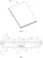
- FIG. 1 is a schematic diagram of a structure of an electronic device in a state according to an embodiment of this application.
- FIG. 2 is a schematic diagram of a structure of the electronic device shown in FIG. 1 that is in a folded state.
- the electronic device 1000 shown in FIG. 1 is in an unfolded state.
- a width direction of the electronic device 1000 is defined as an X-axis direction
- a length direction of the electronic device 1000 is defined as a Y-axis direction
- a thickness direction of the electronic device 1000 is defined as a Z-axis direction. Every two of the X-axis direction, the Y-axis direction, and the Z-axis direction are perpendicular to each other.
- the electronic device 1000 may be an electronic product such as a mobile phone, a tablet computer, a personal digital assistant (personal digital assistant, PDA), a learning machine, a game console, or a notebook computer.
- the electronic device 1000 is a mobile phone.
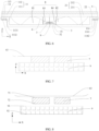
- the mobile phone includes a first body 1, a second body 2, a rotating shaft portion 3, a display 4, a middle cover 5, and a flexible printed circuit 6 ( FIG. 3 is a simplified schematic diagram of a planar structure of the electronic device shown in FIG. 1 , and a specific connection status of the rotating shaft portion 3 is not shown in the figure).
- the first body 1 and the second body 2 are separately connected to the middle cover 5 by using the rotating shaft portion 3, and the first body 1 and the second body 2 may be unfolded or folded relative to each other by using the rotating shaft portion 3.
- a reinforcing plate 7 is fastened to a through-shaft portion of the flexible printed circuit 6, and the reinforcing plate 7 is fixedly connected to the middle cover 5, to fasten the through-shaft portion of the flexible printed circuit 6.
- the display 4 is connected to the first body 1 and the second body 2.
- the first body 1 and the second body 2 When the first body 1 and the second body 2 are unfolded relative to each other, the first body 1 and the second body 2 are distributed side by side in the X-axis direction. An included angle between the first body 1 and the second body 2 is 180 degrees.
- the display 4 is in an unfolded state, and the middle cover 5 is blocked by the first body 1 and the second body 2.
- the first body 1 and the second body 2 are folded relative to each other, the first body 1 and the second body 2 are stacked and distributed in the Z-axis direction. An included angle between the first body 1 and the second body 2 is 0 degrees.
- the display 4 is in a folded state.
- a part of the middle cover 5 is exposed, and the middle cover 5 is located between the first body 1 and the second body 2 and serves as an appearance member of the mobile phone.
- values in a tolerance angle range are allowed in assembly. For example, 179 degrees may be understood as 180 degrees, and 1 degree may be understood as 0 degrees.
- the first body 1 and the second body 2 jointly form an accommodating cavity 8.
- the through-shaft portion and a deformable portion of the flexible printed circuit 6 are located in the accommodating cavity 8.
- the middle cover 5 is located between the first body 1 and the second body 2, and the middle cover 5 is partially or completely located in the accommodating cavity 8.
- the flexible printed circuit 6 connects the first body 1 and the second body 2, so that the first body 1 and the second body 2 perform communication with each other.
- the first body 1 includes a first housing 11 and a first functional module (not labeled in the figure).
- the first functional module is configured to enable the first body 1 to be electrically connected to the second body 2, so that the first body 1 and the second body 2 can transmit information.
- the first housing 11 includes a first middle frame 111 and a first support plate 112.
- the first middle frame 111 and the first support plate 112 form a first accommodating cavity 81.
- the first support plate 112 has a first surface facing away from the first accommodating cavity 81.
- the first surface is configured to support the display 4.
- a first gap is provided between the first middle frame 111 and the first support plate 112, and a second gap 213 is provided between a second middle frame 211 and a second support plate 212 (as shown in FIG.
- Heights of the first gap and the second gap 213 are both greater than a thickness of the flexible printed circuit 6.
- the thickness of the flexible printed circuit 6, the height of the first gap, and the height of the second gap 213 are all dimensions in the X-axis direction, and the first gap and the second gap 213 allow the flexible printed circuit to pass through.
- the first functional module is mounted outside the first accommodating cavity 81.
- the first functional module includes devices such as a first circuit board (printed circuit board, PCB) 12, a processor, a memory, and a communication module.
- the processor, the memory, and the communication module are integrated on the first circuit board 12.
- the memory and the communication module each are electrically connected to the processor.
- the memory is configured to store instructions and data.
- the communication module can implement wireless communication of the mobile phone, such as 3G/4G/5G.
- the communication module can further implement wireless communication such as a wireless local area network (wireless local area networks, WLAN), Bluetooth (bluetooth, BT), and near field communication (near field communication, NFC) of the mobile phone.
- the first functional module may further include devices for implementing other functions. The devices are not enumerated herein.
- the second body 2 includes a second housing 21 and a second functional module (not labeled in the figure).
- the second functional module is configured to enable the second body 2 to be electrically connected to the first body 1, so that the second body 2 and the first body 1 can transmit information.
- a second accommodating cavity 82 is provided in the second housing 21.
- the second housing 21 includes a second middle frame 211 and a second support plate 212.
- the second middle frame 211 and the second support plate 212 form the second accommodating cavity 82.
- the second support plate 212 has a second surface facing away from the second accommodating cavity 82.
- the second surface is configured to support the display 4.
- the second functional module is mounted outside the second accommodating cavity 82.
- the second functional module includes devices such as a second circuit board 22, a battery, an antenna, a motor, and a sensor module.
- the antenna, the motor, and the sensor module are integrated on the second circuit board 22.
- the battery and the second circuit board 22 are stacked or arranged side by side. The stacking arrangement can save space, and the side-by-side arrangement can prevent heat-up of the mobile phone caused by accumulation of heat emitted by the battery and the second circuit board 22.
- the battery provides electric energy for the motor, the sensor module, the antenna, the display 4, and other devices, to ensure normal use of the mobile phone.
- the motor may generate a vibration alert, and may be specifically used for an incoming call vibration alert, or used for touch vibration feedback.
- the sensor module includes a gyroscope sensor, a temperature sensor, and the like.
- the gyroscope sensor may be configured to determine a motion posture of the mobile phone.
- the temperature sensor is configured to detect a temperature, so that the processor executes a temperature processing policy based on the temperature detected by the temperature sensor, to prevent an exception caused by overheat or a low temperature of the mobile phone.
- the second functional module may further include devices for implementing other functions. The devices are not enumerated herein.
- the rotating shaft portion 3 is a hinge, which is connected between the first housing 11 and the second housing 21, and is equivalent to a rotating structure between the first housing 11 and the second housing 21, so that the first housing 11 and the second housing 21 can freely rotate and be folded relative to each other.
- the rotating shaft portion 3 includes two hinges, and the two hinges are respectively arranged on two sides of the mobile phone in the Y-axis direction.
- the rotary shaft portion 3 includes one hinge, and the hinge extends from one side to the other side of the mobile phone in the Y-axis direction.
- the rotating shaft portion 3 is two rotating shafts that are connected and rotatable relative to each other.
- rotating shaft portion 3 may alternatively be a rotating structure of another structure, provided that relative free rotation and relative folding of the first housing 11 and the second housing 21 can be implemented without damaging the display.
- the display 4 is a flexible display, and has properties of being randomly bent, folded, and twisted.
- a display area is large, which facilitates viewing by a user and improves user experience.
- a display area is small, which facilitates an operation performed by a user by a single hand and is convenient for storage and carrying.
- the middle cover 5 is mounted between the first housing 11 and the second housing 21.
- the first housing 11 has a first groove 83
- the second housing 21 has a second groove 84
- the first groove 83 of the first housing 11 is opposite to the second groove 84 of the second housing 21
- the first groove 83 of the first housing 11 communicates with the first accommodating cavity 81
- the second groove 84 of the second housing 21 communicates with the second accommodating cavity 82
- the middle cover 5 is mounted in the first groove 83 and the second groove 84.
- the first accommodating cavity 81, the second accommodating cavity 82, the first groove 83, and the second groove 84 communicate to form the accommodating cavity 8.
- FIG. 8 For ease of distinguishing between parts of the accommodating cavity 8, in FIG.
- the middle cover 5 includes a support groove 51 and an appearance surface 52 facing away from the support groove 51.
- An opening of the support groove 51 faces the accommodating cavity 8.
- a bottom wall of the support groove 51 is used for the through-shaft portion of the flexible printed circuit 6.
- the appearance surface 52 faces away from the accommodating cavity 8.
- the middle cover 5 is prepared by using rigid plastic, so that a weight of the mobile phone can be reduced.
- the through-shaft portion of the flexible printed circuit 6 may be adhesively fastened to the middle cover 5.
- the middle cover 5 is prepared by using a metal or an alloy that can be attracted by a magnetic member.
- the through-shaft portion of the flexible printed circuit 6 may be fastened to the middle cover 5 by attraction of a magnetic force, and does not need to be bonded. This can simplify difficulty in assembling the electronic device.
- FIG. 4 is a schematic diagram of a structure of a flexible printed circuit shown in FIG. 3 .
- the flexible printed circuit 6 is usually prepared by using a polyimide or polyester film as a substrate, and is characterized by free bending, folding, and twisting.
- the flexible printed circuit 6 is configured to connect the first circuit board 12 to the second circuit board 22, so that the devices in the first functional module can be electrically connected to and communicate with the devices in the second functional module.
- the flexible printed circuit 6 includes a first connecting section 61, a first extending section 62, a through-shaft section 63, a second extending section 64, and a second connecting section 65 that are sequentially connected in the X-axis direction.
- the first extending section 62, the through-shaft section 63, and the second extending section 64 are all located in the accommodating cavity 8. Specifically, the first extending section 62 is located in the first accommodating cavity 81, the through-shaft section 63 is located in the first groove 83 and the second groove 84, the second extending section 64 is located in the second accommodating cavity 82, and the first connecting section 61 and the second connecting section 65 are both located outside the accommodating cavity 8. A side of the first connecting section 61 that is close to the first extending section 62 is located in the first gap, and a side of the second connecting section 65 that is close to the second extending section 64 is located in the second gap 213.
- the first connecting section 61 extends out of the first accommodating cavity 81 and is connected to the first circuit board 12, and the first connecting section 61 is soldered and fastened to the first circuit board 12, so that the flexible printed circuit 6 is connected to the first circuit board 12.
- the first connecting section 61 is provided with a first edge connector (not shown in the figure), the first edge connector is formed by arranging, in a finger-like shape, a plurality of conductive contacts whose surface is plated with gold, the first connecting section 61 and the first circuit board 12 are stacked, and the first edge connector is soldered to the first circuit board 12 to electrically connect the flexible printed circuit 6 to the first circuit board 12.
- the first extending section 62 is connected between the first connecting section 61 and the through-shaft section 63.
- the first extending section 62 is located in the first accommodating cavity 81 and is characterized by free bending, folding, and twisting in the first accommodating cavity 81.
- the first extending section 62 can be independently bent and deformed, to adapt to a displacement change occurring when the first body 1 and the second body 2 are bent or unfolded, thereby avoiding breaking the flexible printed circuit 6.
- the through-shaft section 63 is located at the rotating shaft portion 3, so that the flexible printed circuit 6 passes through the rotating shaft portion 3 to electrically connect the first body 1 to the second body 2.
- the reinforcing plate 7 is provided on one surface of the rotating shaft portion 3, and the reinforcing plate 7 is adhesively fastened to a surface of the through-shaft section 63.
- the reinforcing plate 7 can increase structural strength of the through-shaft section 63 and prevent the through-shaft section 63 from being broken during repeated folding and unfolding of the mobile phone. Before the flexible printed circuit 6 is assembled to the mobile phone, the reinforcing plate 7 has been previously bonded to the through-shaft section of the flexible printed circuit 6.
- a surface of the reinforcing plate 7 that faces away from the through-shaft section 63 is fixedly connected to the middle cover 5, to prevent a location of the flexible printed circuit 6 from being displaced.
- the second extending section 64 is located in the second accommodating cavity 82 and is characterized by free bending, folding, and twisting in the second accommodating cavity 82. When the mobile phone is folded or unfolded, the second extending section 64 can be independently bent and deformed, to adapt to a displacement change occurring when the first body 1 and the second body 2 are bent or unfolded, thereby avoiding breaking the flexible printed circuit 6.
- FIG. 5 is an enlarged view of a location A in FIG. 3 .
- the second connecting section 65 extends out of the second accommodating cavity 82 and is connected to the second circuit board 22, so that the flexible printed circuit 6 is connected to the second circuit board 22, and the second connecting section 65 is soldered and fastened to the second circuit board 22.
- the second connecting section 65 is provided with a second edge connector, the second edge connector is formed by arranging, in a finger-like shape, a plurality of conductive contacts whose surface is plated with gold, the second connecting section 65 and the second circuit board 22 are stacked, and the second edge connector is soldered to the second circuit board 22 to electrically connect the flexible printed circuit 6 to the second circuit board 22.
- the first circuit board 12 and the second circuit board 22 are connected by using the flexible printed circuit 6, to electrically connect the devices in the first functional module to the devices in the second functional module.
- devices such as the battery, the antenna, the motor, and the sensor module in the second functional module may all be connected to the processor in the first functional module by using the flexible printed circuit 6.
- the antenna in the second functional module may further be connected to the communication module in the first functional module by using the flexible printed circuit 6.
- the first connecting section 61 is soldered and fastened to the first circuit board 12 by using the first edge connector
- the second connecting section 65 is soldered and fastened to the second circuit board 22 by using the second edge connector.
- the first edge connector and the second edge connector are respectively provided on surfaces of the first connecting section 61 and the second connecting section 65 of the flexible printed circuit, or may be respectively provided on surfaces of the first circuit board 12 and the second circuit board 22, provided that the flexible printed circuit 6 can be electrically connected to the first circuit board 12 and the second circuit board 22.
- fastening is implemented by soldering, and the thicknesses of the connection joints each are less than or equal to 0.3 mm. This improves structural compactness of internal devices of the mobile phone, increases space utilization, reduces an overall thickness of the mobile phone, and facilitates a light and thin design of the mobile phone.
- the thickness of the connection joint between the first circuit board 12 and the flexible printed circuit 6 and the thickness of the connection joint between the second circuit board 22 and the flexible printed circuit 6 are greatly reduced.
- a side of the first middle frame 111 that is away from the second middle frame 211 is provided with a first bearing plate 113.
- the first bearing plate 113 is located outside the accommodating cavity 8.
- the first bearing plate 113 includes a first bearing surface 1131 and a second bearing surface 1132 opposite to the first bearing surface 1131.
- the first connecting section 61 of the flexible printed circuit 6 is stacked on the first bearing surface 1131 of the first bearing plate 113.
- a side of the second middle frame 211 that is away from the first middle frame 111 is provided with a second bearing plate 114.
- the second bearing plate 114 is located outside the accommodating cavity 8.
- the second bearing plate 114 includes a third bearing surface 1141 and a fourth bearing surface 1142 opposite to the third bearing surface 1141.
- the second connecting section 65 of the flexible printed circuit 6 is stacked on the third bearing surface 1141 of the second bearing plate 114.
- the first bearing surface 1131 of the first bearing plate 113 is provided with a first accommodating groove.
- the third bearing surface 1141 of the second bearing plate 114 is provided with a second accommodating groove.
- the first accommodating groove and the second accommodating groove are configured to respectively accommodate the first circuit board 12 and the second circuit board 22, and respectively accommodate the first connecting section 61, of the flexible printed circuit 6, that is soldered to the first circuit board 12 and provided with the first edge connector, and the second connecting section 65, of the flexible printed circuit 6, that is soldered to the second circuit board 22 and provided with the second edge connector, so that the overall thickness of the mobile phone can be reduced in the Z-axis direction.
- FIG. 6 is a schematic diagram of a planar structure of an electronic device according to another embodiment.
- the first connecting section 61 of the flexible printed circuit 6 is stacked on the second bearing surface 1132 of the first bearing plate 113, and the second connecting section 65 of the flexible printed circuit 6 is stacked on the fourth bearing surface 1142 of the second bearing plate 114.
- FIG. 7 is a schematic diagram of a planar structure in which a fastening block shown in FIG. 3 fastens a through-shaft section of a flexible printed circuit.
- a fastening block 9 fixedly connected to the middle cover 5 is provided on the middle cover 5.
- the fastening block 9 and the middle cover 5 may be integrally formed, and the fastening block 9 is a part of the middle cover 5.
- the fastening block 9 and the middle cover 5 may be separately formed, and the fastening block 9 is connected to the bottom wall of the support groove 51 of the middle cover 5.
- the reinforcing plate 7 is fixedly connected to the middle cover 5 by using the fastening block 9.
- the reinforcing plate 7 and the flexible printed circuit 6 are also disassembled.
- the fastening block 9 is a magnet with a magnetic property.
- the reinforcing plate 7 is prepared by using a metal or an alloy that can be attracted by a magnetic member.
- the metal that can be attracted by a magnetic member includes iron, cobalt, nickel, and the like, and the alloy that can be attracted by a magnetic member includes an iron-nickel alloy, an aluminum-iron alloy, an aluminum-nickel-cobalt alloy, and the like, so that the reinforcing plate 7 is magnetically fastened to the fastening block 9.
- FIG. 8 is a schematic diagram of a breakdown structure of FIG. 7 .
- the reinforcing plate 7 has a first reinforcing surface 71 and a second reinforcing surface 72 that are opposite to each other.
- the first reinforcing surface 71 is adhesively fastened to the through-shaft section 63 of the flexible printed circuit 6.
- the second reinforcing surface 72 faces the fastening block 9 and is fixedly connected to the fastening block 9 by using a magnetic force.
- the reinforcing plate 7 prepared by using a metal or an alloy that can be attracted by a magnetic member has high structural strength. This can improve strength of the through-shaft section 63 and facilitate overall assembly of the mobile phone. There is a magnetic attraction force between the reinforcing plate 7 and the fastening block 9, so that the flexible printed circuit 6 can be fastened, and disassembly of the flexible printed circuit 6 can be facilitated.
- the fastening block 9 has a magnetic surface and the reinforcing plate 7 also has a magnetic surface.
- the magnetic surface of the fastening block 9 and the magnetic surface of the reinforcing plate 7 can be attracted to each other, thereby fastening the reinforcing plate 7 by using the fastening block 9.
- the fastening block 9 has a first fastening surface 91 and a second fastening surface 92 that are opposite to each other.
- the first fastening surface 91 has a first magnetic pole and the second fastening surface 92 has a second magnetic pole.
- the first magnetic pole and the second magnetic pole are opposite to each other.
- the first magnetic pole is an N pole
- the second magnetic pole is an S pole. Therefore, the fastening block 9 is enabled to impose a magnetic attraction force on the reinforcing plate 7, so as to fasten the through-shaft section 63 of the flexible printed circuit 6.
- the first pole is an S pole and the second pole is an N pole.
- the first fastening surface 91 faces the reinforcing plate 7, and is magnetically connected to the second reinforcing surface 72 of the reinforcing plate 7.
- the second fastening surface 92 faces the middle cover 5, and is adhesively fastened and/or magnetically fastened to the bottom wall of the support groove 51 of the middle cover 5.
- the fastening block 9 is configured to fasten the reinforcing plate 7 to increase fastening reliability of the flexible printed circuit 6.
- a fastening force between the fastening block 9 and the middle cover 5 is greater than that between the fastening block 9 and the reinforcing plate 7, thereby preventing the fastening block 9 from loosening during the disassembly of the flexible printed circuit 6.
- the middle cover 5 is prepared by using a metal or an alloy that can be attracted by a magnetic member.
- the second fastening surface 92 of the fastening block 9 is fastened to the bottom wall of the support groove 51 of the middle cover 5 by using a magnetic force.
- a bonding force may exist between the middle cover 5 and the fastening block 9, thereby increasing fastening strength of the fastening block 9.
- the middle cover 5 is prepared by using rigid plastic without a magnetic property.
- the second fastening surface 92 of the fastening block 9 is adhesively fastened to the bottom wall of the support groove 51.
- the reinforcing plate 7 is directly fixedly connected to the middle cover 5.
- the second reinforcing surface 72 of the reinforcing plate 7 is adhesively or magnetically fastened to the bottom wall of the support groove 51 of the middle cover 5.
- the second reinforcing surface 72 of the reinforcing plate 7 is magnetically fastened to the bottom wall of the support groove 51 of the middle cover 5.
- Both the second reinforcing surface 72 and the bottom wall of the support groove 51 are magnetic surfaces, and the two magnetic surfaces can be attracted to each other to fixedly connect the reinforcing plate 7 to the middle cover 5. This can simplify a structure of the mobile phone and reduce a complexity degree of the structure of the mobile phone.
- the second reinforcing surface 72 of the reinforcing plate 7 is fastened to the bottom wall of the support groove 51 of the middle cover 5.
- both the reinforcing plate 7 and the middle cover 5 may be prepared by using lightweight rigid plastic, thereby reducing the weight of the mobile phone.
- the reinforcing plate 7 includes a support sheet 73 and a flexible region 74.
- the flexible region 74 divides the support sheet 73 into a plurality of sheet bodies 731, and the support sheet 73 is fixedly connected to the fastening block 9.
- the flexible region 74 enables the reinforcing plate 7 to be flexibly deformed during movement of the flexible printed circuit.
- the flexible region 74 enables the reinforcing plate 7 to have at least a capability of being bent and deformed in a length direction (the Y-axis direction) of the reinforcing plate 7, and the length direction of the reinforcing plate 7 is the same as the length direction (the Y-axis direction) of the electronic device 1000.
- the support sheet 73 is prepared by using a metal material with specific rigidity, such as a steel plate or another metal plate body.
- the support sheet 73 is configured to support the flexible printed circuit 6 and to enhance structural stability of the through-shaft section 63 of the flexible printed circuit 6.
- the reinforcing plate 7 including the flexible region 74 can ensure that the flexible printed circuit 6 is withdrawn without device disassembly, thereby preventing damage to the display or a rotating shaft structure.
- FIG. 9 is a schematic diagram of a case in which a support sheet of a reinforcing plate in an embodiment of the electronic device shown in FIG. 3 is mounted on a flexible printed circuit, where the support sheet has two sheet bodies.
- the support sheet 73 has two strip-shaped sheet bodies 731.
- the two sheet bodies 731 are mounted on the flexible printed circuit 6, the two sheet bodies 731 are fastened to a surface of the through-shaft section 63.
- a quantity and shapes of the support sheets 73 may be set to other forms, and shapes and a quantity of the spacings 741 forming the flexible region 74 may also be set to other forms.
- the support sheet 73 that is, the two sheet bodies 731, of the reinforcing plate 7 may be bonded by using an adhesive film. Then, a side surface, of the adhesive film, to which the reinforcing plate 7 is bonded is made face the through-shaft section 63 of the flexible printed circuit 6, to transfer the reinforcing plate 7 to the flexible printed circuit 6 and then remove the adhesive film.
- the adhesive film is specifically adhesive tape, a plastic film coated with an adhesive layer, or the like.
- the support sheet 73 is fixedly connected to the fastening block 9, and the flexible region 74 is not connected to the fastening block 9. Therefore, there is no fastening force between the flexible region 74 and the fastening block 9.
- a contact area between each sheet body of the support sheet 73 and the fastening block 9 is less than a contact area between a whole sheet-like reinforcing plate including all sheet bodies and the fastening block 9 in a same area. Therefore, a fastening force between each sheet body and the fastening block 9 is less than a fastening force, in a same area, between the whole sheet-like reinforcing plate including all sheet bodies and the fastening block 9.
- the flexible printed circuit 6 When the flexible printed circuit 6 becomes faulty and needs to be repaired or replaced, a rear cover of the mobile phone is removed, and at least parts of the first connecting section 61 and the second connecting section 65 are in a visible state. Then, the flexible printed circuit 6 can be withdrawn from the first body 1 and the second body 2 of the mobile phone in a width direction (the X-axis direction) of the mobile phone by applying a force on the first connecting section 61 or the second connecting section 65 in the visible state by using a tools such as tweezers or by using a finger directly.
- a tools such as tweezers or by using a finger directly.
- solder joint between the first connecting section 61 and the first circuit board 12 is first removed by using a tool, or a force is directly applied to the first connecting section 61 to separate the first connecting section 61 from the first circuit board 12.
- a solder joint between the second connecting section 65 and the second circuit board 22 is removed by using a tool, or a force is directly applied to the second connecting section 65 to separate the second connecting section 65 from the second circuit board 22.
- the first connecting section 61 is pulled, so that a sheet body close to the first connecting section 61 is separated from the fastening block.
- the first connecting section 61 continues to be pulled, so that a sheet body close to the second connecting section 65 is separated from the fastening block.
- the flexible printed circuit is withdrawn from left to right (a direction in FIG. 3 ).
- the flexible printed circuit 6 is withdrawn, except the first connecting section 61, remaining parts of the flexible printed circuit 6 sequentially pass through the second gap 213, the accommodating cavity 8, and the first gap, and the flexible printed circuit 6 is finally completely withdrawn.
- a force may alternatively be applied to the second connecting section 65 to withdraw the flexible printed circuit from right to left.
- the second connecting section 65 remaining parts of the flexible printed circuit 6 sequentially pass through the first gap, the accommodating cavity 8, and the second gap 213, and the flexible printed circuit 6 is finally completely withdrawn.
- FIG. 10 is a schematic diagram of a structure in which the reinforcing plate shown in FIG. 9 is bent and deformed under driving by a through-shaft section of a flexible printed circuit.
- the fastening force between the reinforcing plate 7 and the fastening block 9 is small and the flexible region 74 can enable the reinforcing plate 7 to be bent and deformed, when the flexible printed circuit 6 is withdrawn, the flexible printed circuit 6 is moved to drive the flexible region 74 to be deformed, so that the reinforcing plate 7 as a whole is bent and deformed in the length direction of the reinforcing plate 7.
- the fastening force imposed on the reinforcing plate 7 is dispersed by a plurality of support sheets.
- one support sheet 73 can be separated from the fastening block 9 by using a small force, and then another sheet body 731 can be separated from the fastening block 9 by using a small force.
- the flexible printed circuit 6 is withdrawn as a whole. No device disassembly is needed throughout a process of withdrawing the flexible printed circuit 6. This avoids disassembling the display 4 or the middle frame, ensures smooth replacement of the flexible printed circuit 6, and avoids damage to the display or a folding structure during the replacement of the flexible printed circuit 6.
- Another flexible printed circuit is mounted on the mobile phone.
- This flexible printed circuit is pre-assembled with a reinforcing plate, and then a second connecting section is inserted into the accommodating cavity 8 from the first gap between the first middle frame 111 and the first support plate 112, and after passing over the fastening block 9 in the accommodating cavity 8, the second connecting section extends out of the accommodating cavity 8 from the second gap 213 between the second middle frame 211 and the second support plate 212.
- a first connecting section is temporarily fastened, and a force is applied to the second connecting section, so that a second extending section extends out of the accommodating cavity 8, until it is perceived that an attraction force is generated between the reinforcing plate 7 on a through-shaft section and the fastening block 9.
- the through-shaft section corresponds to the fastening block 9 and is fastened to the fastening block 9 by attraction.
- the second extending section is inserted into the accommodating cavity 8 again, and finally the first connecting section is soldered to the first circuit board 12, and the second connecting section is soldered to the second circuit board 22, to complete mounting of the another flexible printed circuit.
- the first connecting section may alternatively be inserted into the accommodating cavity 8 from the second gap 213.
- the second connecting section other parts of the flexible printed circuit sequentially pass through the second gap 213 and enter the accommodating cavity, and the first connecting section then passes through the first gap from the accommodating cavity 8, so as to extend out of the accommodating cavity 8.
- FIG. 11 is a schematic diagram of a structure of a reinforcing plate in an embodiment of the electronic device shown in FIG. 3 .
- the flexible region 74 may be prepared by using a flexible material that connects the support sheet 73.
- the flexible material is a plastic film
- a film layer prepared by using the flexible material forms the flexible region 74.
- the reinforcing plate 7 can be directly fastened to the through-shaft section 63 of the flexible printed circuit 6 without assistance from an additional tool, thereby simplifying an assembly process and saving an assembly time.
- the support sheet 73 has a plurality of sheet bodies 731 arranged in an array, and the flexible region 74 is formed when the support sheet 73 is mounted on the flexible printed circuit 6.
- a plurality of means two or more.
- FIG. 12 is a schematic diagram of a case in which a support sheet of a reinforcing plate in an embodiment of the electronic device shown in FIG. 3 is mounted on a flexible printed circuit, where the support sheet has five sheet bodies.
- the support sheet 73 has five strip-shaped sheet bodies 731.
- a strip-shaped spacing 741 exists between any two adjacent sheet bodies 731 in the X-axis direction.
- the five sheet bodies 731 form four spacings 741, and the four spacings 741 and the five sheet bodies 731 are alternately distributed in the X-axis direction of the reinforcing plate 7.
- FIG. 14 is a schematic diagram of a case in which a support sheet of a reinforcing plate in an embodiment of the electronic device shown in FIG. 3 is mounted on a flexible printed circuit, where the support sheet has a plurality of sheet bodies.
- the support sheet 73 has square sheet bodies 731 arranged in 10 rows and 5 columns.
- a spacing 741 exists between any two adjacent sheet bodies 731, and the spacings 741 are connected to each other.
- a plurality of sheet bodies 731 are arranged out of order, and the sheet bodies 731 are triangular, circular, pentagonal, hexagonal, trapezoidal, or elliptical in shape.
- "a plurality of” means two or more.
- the reinforcing plate 7 is integrally formed and has a plurality of spacings 741. This not only can improve assembly convenience, but also can improve convenience in withdrawing the flexible printed circuit 6.
- a quantity of spacings 741 forming the flexible region 74 increases, a quantity of locations at which the reinforcing plate 7 can be deformed increases, and a flexibility degree also increases.
- a larger quantity and a larger total area of spacings 741 forming the flexible region 74 indicates a smaller contact area between the reinforcing plate 7 and the fastening block 9 and a smaller fastening force between the reinforcing plate 7 and the fastening block 9.
- a higher flexibility degree of the reinforcing plate 7 indicates a larger quantity of locations at which deformation occurs and more dispersed fastening forces between the reinforcing plate 7 and the fastening block 9. Therefore, FIG.
- FIG. 13 is a schematic diagram of a structure in which the reinforcing plate shown in FIG. 12 is bent and deformed under driving by a through-shaft section of a flexible printed circuit.
- the reinforcing plate 7 is deformed at a plurality of locations. With the locations corresponding to deformation being used as a separation line, it is equivalent that the reinforcing plate 7 is divided into a plurality of parts and withdrawn. A smaller force is needed each time one part is withdrawn, so that the flexible printed circuit 6 can be conveniently withdrawn.
- the reinforcing plate 7 includes the five sheet bodies 731 shown in FIG. 12 serving as the support sheet 73. A difference from the reinforcing plate 7 shown in FIG. 12 lies in that, a film layer formed by a flexible material is provided in the four spacings 741 to serve as the flexible region 74.
- the reinforcing plate includes the plurality of sheet bodies 731 shown in FIG. 14 serving as the support sheet 73. A difference from the reinforcing plate 7 shown in FIG. 14 lies in that, a film layer formed by a flexible material is provided in the plurality of spacings 741 to serve as the flexible region 74.
- the reinforcing plate 7 can be directly fastened to the through-shaft section 63 of the flexible printed circuit 6 without assistance from an additional tool, thereby simplifying an assembly process and saving an assembly time.
- the flexible region 74 is provided on the support sheet 73 of the reinforcing plate 7.
- FIG. 15 is a schematic diagram of a case in which a flexible region of a reinforcing plate in an embodiment of the electronic device shown in FIG. 3 is provided on a support sheet of the reinforcing plate, where the flexible region includes one hollow region.
- the flexible region 74 is a hollow region 742 provided on the support sheet 73 and extending in the Y-axis direction of the reinforcing plate 7. An axis of the hollow region 742 in the Y-axis direction coincides with an axis of the reinforcing plate 7 in the Y-axis direction.
- the support sheet 73 is a sheet body that surrounds the hollow region 742, and the hollow region 742 is strip-shaped.
- the axis of the hollow region 742 in the Y-axis direction is staggered with the axis of the reinforcing plate 7 in the Y-axis direction, and the hollow region 742 has an elliptical, rectangular, or trapezoidal shape.
- the support sheet 73 surrounds the hollow region 742. This can increase structural strength of the reinforcing plate 7 and facilitate mounting.
- a contact area between the support sheet 73 and the fastening block 9 is less than a contact area between a whole sheet-like reinforcing plate provided with no hollow region and the fastening block 9 in a same area. Therefore, a fastening force between the support sheet 73 and the fastening block 9 is less than a fastening force, in a same area, between the whole sheet-like reinforcing plate provided with no hollow region and the fastening block 9, and there is no fastening force between the hollow region 742 and the fastening block 9. Compared with that of a conventional reinforcing plate, the fastening force between the reinforcing plate 7 and the fastening block 9 is significantly reduced.
- the flexible region 74 further enables the reinforcing plate 7 to be deformed in the Y-axis direction.
- the fastening force between the reinforcing plate 7 and the fastening block 9 is dispersed into a plurality of smaller forces.
- FIG. 16 is a schematic diagram of a structure in which the reinforcing plate shown in FIG. 15 is bent and deformed under driving by a through-shaft section of a flexible printed circuit.
- the flexible printed circuit 6 As the fastening force between the reinforcing plate 7 and the fastening block 9 is small and the flexible region 74 can enable the reinforcing plate 7 to be bent and deformed, when the flexible printed circuit 6 is withdrawn, the flexible printed circuit 6 is moved to drive the flexible region 74 to be deformed, so that the reinforcing plate 7 as a whole is bent and deformed in the length direction of the reinforcing plate 7.
- two parts of the support sheet 73 that are located on two sides of the hollow region 742 may be separately separated from the fastening block 9. A force needed for separating each part is small.
- the flexible printed circuit 6 is withdrawn as a whole. No device disassembly is needed throughout a process of withdrawing the flexible printed circuit 6. This ensures smooth replacement of the flexible printed circuit 6, and avoids damage to the display or a folding structure during the replacement of the flexible printed circuit 6.
- FIG. 17 is a schematic diagram of a case in which a flexible region of a reinforcing plate in an embodiment of the electronic device shown in FIG. 3 is provided on a support sheet of the reinforcing plate, where the flexible region includes three hollow regions arranged along an X-axis.
- the flexible region 74 is provided on the support sheet 73 of the reinforcing plate 7.
- the flexible region 74 has a plurality of hollow regions 742 provided on the support sheet 73.
- the support sheet 73 is a sheet body 731, and the plurality of hollow regions 742 are arranged in an array on the sheet body 731.
- the flexible region 74 specifically has three square hollow regions 742 extending in the Y-axis direction.
- FIG. 18 is a schematic diagram of a structure in which the reinforcing plate shown in FIG. 17 is bent and deformed under driving by a through-shaft section of a flexible printed circuit. Bending and deformation occur at a plurality of locations in the Y-axis direction, thereby reducing the fastening force between the reinforcing plate 7 and the fastening block.
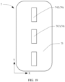
- FIG. 19 is a schematic diagram of a case in which a flexible region of a reinforcing plate in an embodiment of the electronic device shown in FIG. 3 is provided on a support sheet of the reinforcing plate, where the flexible region includes three hollow regions arranged along a Y-axis. Specifically, the three hollow regions 742 are distributed at spacings 741 in the Y-axis direction of the sheet body 731.
- the reinforcing plate 7 has high structural strength, and can be bent and deformed in the Y-axis direction, to disperse the fastening force between the reinforcing plate 7 and the fastening block 9.
- FIG. 19 is a schematic diagram of a case in which a flexible region of a reinforcing plate in an embodiment of the electronic device shown in FIG. 3 is provided on a support sheet of the reinforcing plate, where the flexible region includes three hollow regions arranged along a Y-axis. Specifically, the three hollow regions 742 are distributed at spacings 741 in the Y-axis
- FIG. 20 is a schematic diagram of a case in which a flexible region of a reinforcing plate in an embodiment of the electronic device shown in FIG. 3 is provided on a support sheet of the reinforcing plate, where the flexible region includes a plurality of hollow regions arranged in an array.
- the flexible region 74 includes elliptical hollow regions 742 arranged in 7 rows and 5 columns.
- the reinforcing plate 7 can be bent and deformed at a plurality of locations in the Y-axis direction, to disperse the fastening force between the reinforcing plate 7 and the fastening block 9.
- a plurality of hollow regions 742 are arranged out of order, and the hollow regions 742 are triangular, circular, pentagonal, hexagonal, trapezoidal, or elliptical in shape.
- a quantity of hollow regions 742 increases, a quantity of locations at which the reinforcing plate 7 can be deformed increases, and a flexibility degree also increases.
- a larger quantity and a larger total area of hollow regions 742 indicates a smaller contact area between the reinforcing plate 7 and the fastening block 9 and a further reduced fastening force between the reinforcing plate 7 and the fastening block 9.
- a higher flexibility degree of the reinforcing plate 7 indicates a larger quantity of locations at which deformation occurs and more dispersed fastening forces between the reinforcing plate 7 and the fastening block 9. Therefore, when the flexible printed circuit 6 is withdrawn, on a premise that a total fastening force decreases, the reinforcing plate 7 is deformed at a plurality of locations.
- the reinforcing plate 7 is divided into a plurality of parts and withdrawn. A smaller force is needed each time one part is withdrawn, so that the flexible printed circuit 6 can be conveniently withdrawn.
- the reinforcing plate 7 includes the support sheet 73 and the flexible region that are shown in FIG. 15 .
- a difference from the reinforcing plate 7 shown in FIG. 15 lies in that, the flexible region is prepared by using a film layer formed by a flexible material, to replace the hollow region shown in FIG. 15 .
- the reinforcing plate 7 includes the support sheet 73 shown in FIG. 17 .
- a difference from the reinforcing plate 7 shown in FIG. 17 lies in that, a film layer formed by a flexible material is provided in the three hollow regions distributed in the X-axis direction, to serve as the flexible region 74.
- the reinforcing plate 7 includes the support sheet 73 shown in FIG. 19 .
- the reinforcing plate 7 can be directly fastened to the through-shaft section 63 of the flexible printed circuit 6 without assistance from an additional tool, thereby simplifying an assembly process and saving an assembly time.
- the reinforcing plate 7 is prepared by using a cutting method or an etching method. Specifically, an integral sheet material is etched by using the etching method to obtain a hollow region 742, the hollow region 742 forms the flexible region 74, and an unetched sheet body 731 forms the support sheet 73, thereby preparing the reinforcing plate 7.
- an integral sheet material may alternatively be cut into a plurality of sheet bodies 731 by using the cutting method, and some of the sheet bodies 731 may be removed.
- a length of the reinforcing plate 7 is from 18 mm to 22 mm, a width of the reinforcing plate 7 is from 5 mm to 7 mm, and a thickness of the reinforcing plate 7 is from 0.1 mm to 0.3 mm.
- the length of the reinforcing plate 7 is 18 mm, 19 mm, 20 mm, 21 mm, or 22 mm, the width of the reinforcing plate 7 is 5 mm, 6 mm, or 7 mm, and the thickness of the reinforcing plate 7 is 0.1 mm, 0.2 mm, or 0.3 mm.
- FIG. 21 is a schematic diagram of a planar structure of an electronic device including a press-fit plate.
- the electronic device further includes a press-fit plate 10.
- a length of the press-fit plate 10 in the Y-axis direction is greater than that of the flexible printed circuit 6 in the Y-axis direction.
- Connecting wings are respectively provided at two opposite ends of the press-fit plate 10 in the Y-axis direction.
- the press-fit plate 10 is fixedly connected to the bottom wall of the support groove 51 by using the connecting wings. Specifically, the connecting wings are fastened to the bottom wall of the support groove by using screws.
- the press-fit plate 10 has a press-fit surface 101 facing the reinforcing plate 7, there is a spacing between the press-fit surface 101 and a surface of the through-shaft section that faces away from the reinforcing plate 7, and the spacing is greater than 1.3 mm and less than or equal to 1.7 mm in the Z-axis direction.
- the spacing is 1.3 mm, 1.5 mm, or 1.7 mm.
- the press-fit plate 10 plays a function of shaping the through-shaft section 63.
Landscapes
- Engineering & Computer Science (AREA)
- Computer Hardware Design (AREA)
- Theoretical Computer Science (AREA)
- Physics & Mathematics (AREA)
- General Engineering & Computer Science (AREA)
- Signal Processing (AREA)
- Human Computer Interaction (AREA)
- General Physics & Mathematics (AREA)
- Microelectronics & Electronic Packaging (AREA)
- Computer Networks & Wireless Communication (AREA)
- Mathematical Physics (AREA)
- Telephone Set Structure (AREA)
- Casings For Electric Apparatus (AREA)
Abstract
Description
- This application claims priority to
Chinese Patent Application No. 2021112192356, filed with the China National Intellectual Property Administration on October 20, 2021 - This application relates to the technical field of foldable communication devices, in particular, to an electronic device.
- With development of science and technology, various electronic devices gradually become an indispensable part of life. For example, a mobile phone is provided with an increasingly large display to improve user experience and increase use functions of the mobile phone. To increase a display area of the mobile phone while reducing a volume of the mobile phone, a foldable mobile phone emerges.
- In an existing foldable mobile phone, a display is supported by two bodies that are rotatably connected by using a folding structure, and the display can be unfolded or folded in a relative manner by using the two bodies, to implement unfolded and folded states of the display. The two bodies are provided with different circuit modules. To implement electrical connection and communication between the two circuit modules in the two bodies, the existing foldable mobile phone is provided with a flexible printed circuit (flexible print circuit, FPC), and the two circuit modules are electrically connected by using the flexible printed circuit. However, if the flexible printed circuit becomes faulty during subsequent use and needs to be replaced, the display and the bodies need be disassembled, which is inconvenient for repair and replacement.
- This application provides an electronic device, to resolve a technical problem that repair is inconvenient because a whole device needs to be disassembled when a flexible printed circuit is replaced.
- An electronic device provided in an embodiment of this application includes a first body, a second body, a rotating shaft portion, a display, a middle cover, and a flexible printed circuit.
- The first body is connected to one side of the middle cover by using the rotating shaft portion, the second body is connected to the other side of the middle cover by using the rotating shaft portion, the display is connected to the first body and the second body, and the electronic device includes a gap connecting the first body, the second body, and the middle cover. The rotating shaft portion makes both the first body and the second body rotatable. The display is specifically a flexible display that can be deformed and bent. The first body and the second body may be unfolded or folded relative to each other. When the first body and the second body are unfolded relative to each other, the display is in an unfolded state, and a display area is large. When the first body and the second body are folded relative to each other, the display is in a folded state.
- The flexible printed circuit is located in the gap and extends from the first body to the second body, to connect the first body and the second body. The first body includes a first functional module, the second body includes a second functional module, and the flexible printed circuit is specifically connected to the first functional module and the second functional module, so that the first functional module and the second functional module are electrically connected.
- The flexible printed circuit includes a through-shaft section, and a reinforcing plate is provided on a surface of the through-shaft section. The reinforcing plate can increase strength of the through-shaft section, to prevent a through-shaft portion from being damaged or broken during repeated unfolding and folding of the electronic device.
- The reinforcing plate is located in the middle cover, the reinforcing plate includes a support sheet and a flexible region, and a surface of the support sheet that faces away from the through-shaft section is fastened to the middle cover. The flexible region is provided on the support sheet or divides the support sheet into a plurality of sheet bodies, and the support sheet or the sheet body is stacked on and fastened to a surface of the through-shaft section. The reinforcing plate is fastened to the middle cover by using the support sheet, the flexible region is not connected to the middle cover, and there is no fastening force between the flexible region and the middle cover.
- In this embodiment, the reinforcing plate includes the support sheet and the flexible region. Because there is no fastening force between the flexible region and the middle cover, a fastening force between the reinforcing plate and the middle cover in this embodiment is significantly less than that caused by a reinforcing plate with a same area. A fastening force to be overcome during replacement of the flexible printed circuit is small. The flexible region further enables the reinforcing plate to be flexibly deformed when the flexible printed circuit is moved. Specifically, the flexible region of the reinforcing plate enables the reinforcing plate to be deformed and bent in at least a length direction of the electronic device. Therefore, when the flexible printed circuit is disassembled, the fastening force between the reinforcing plate and the middle cover is dispersed into a plurality of small portions as the reinforcing plate is bent and deformed. In this way, the flexible printed circuit can be withdrawn and replaced without disassembling the display and the body structures, thereby improving convenience in repairing and replacing the flexible printed circuit. As the flexible printed circuit can be replaced without disassembling the display and the body structures, damage to the display or a middle frame occurring during replacement of the flexible printed circuit can be avoided, thereby prolonging a lifetime of the electronic device.
- In an embodiment, the reinforcing plate is adhesively fastened to the middle cover. Specifically, the support sheet is adhesively fastened to the middle cover. During mounting, adhesive is dispensed on a surface of the support sheet that faces away from the through-shaft portion. When the flexible printed circuit is mounted in the electronic device, an adhesive-dispensing portion is in contact with the middle cover to fasten the flexible printed circuit. The adhesive fastening manner has high reliability, and can prevent the whole flexible printed circuit from being displaced due to loosening of the through-shaft portion, and avoid instable electrical connection between the first body and the second body that is caused by the displacement of the flexible printed circuit, thereby improving stability of the electrical connection.
- In an embodiment, the reinforcing plate has a magnetic surface, the middle cover has a magnetic surface, and the reinforcing plate and the middle cover are fastened by magnetic attraction. Specifically, the reinforcing plate may be prepared by using a material that can be attracted by a magnetic member, for example, prepared by using steel, and a surface of the reinforcing plate that faces the middle cover is a magnetic surface. A layer of magnet is provided on the middle cover, and a surface of the magnet that faces the reinforcing plate is the magnetic surface of the middle cover. The magnet can generate an attraction force on the reinforcing plate prepared by using steel, to fasten the through-shaft section of the flexible printed circuit.
- In an embodiment, the reinforcing plate is fastened in the middle cover by using a fastening block, the fastening block is magnetic and fastened in the middle cover, and the reinforcing plate is magnetically connected to the fastening block. Specifically, the fastening block is a magnet, the reinforcing plate is prepared by using steel, the reinforcing plate has a first reinforcing surface and a second reinforcing surface opposite to the first reinforcing surface, the fastening block includes a first fastening surface and a second fastening surface opposite to the first fastening surface, a magnetic pole of the first fastening surface is an N pole, and a magnetic pole of the second fastening surface is an S pole. The first reinforcing surface is adhesively fastened to the through-shaft section of the flexible printed circuit, so that the reinforcing plate is fastened to the flexible printed circuit, the second reinforcing surface is magnetically fastened to the first fastening surface, and the second fastening surface is fastened to the middle cover by attraction.
- The reinforcing plate is fastened by using the magnet. This not only can ensure reliable connection between the through-shaft section of the flexible printed circuit and the middle cover, but also can improve convenience in disassembling the flexible printed circuit and reduce disassembly difficulty in withdrawing the flexible printed circuit when the electronic device is not disassembled. Specifically, when the flexible printed circuit needs to be disassembled, an N pole of a magnet is made to approach the display of the electronic device. In this case, a repulsion force is generated between the magnet and the N pole of the fastening block, so that an attraction force imposed by the fastening block on the reinforcing plate is weakened. After the attraction force is weakened, the flexible printed circuit can be more easily withdrawn from the electronic device.
- In an embodiment, the support sheet includes a plurality of individual sheet bodies, and the flexible region is formed when the sheet bodies are mounted on the flexible printed circuit. Specifically, when the plurality of sheet bodies are mounted on the flexible printed circuit, the sheet bodies are spaced, and a spacing between every two adjacent sheet bodies form the flexible region. Because two adjacent sheet bodies are totally isolated, the flexible region formed can make the reinforcing plate have a very strong flexible deformation capability. When the flexible printed circuit is withdrawn, the fastening force for fastening the reinforcing plate is effectively dispersed, and this can reduce difficulty in disassembling the flexible printed circuit.
- In an embodiment, the support sheet includes two individual sheet bodies. The two individual sheet bodies are spaced on the through-shaft section of the flexible printed circuit along a width direction of the electronic device. In this case, a spacing extending in the length direction of the electronic device is formed between the two sheet bodies, and this spacing forms the flexible region. A reinforcing plate including two individual sheet bodies is easy to mount.
- In an embodiment, the flexible region is a hollow region running through the support sheet. In this case, the support sheet maintains an integral state. This can simplify a step of mounting the reinforcing plate onto the through-shaft section of the flexible printed circuit, improve assembly convenience, and enable the reinforcing plate to have a flexible deformation capability.
- In an embodiment, there are a plurality of hollow regions, and the plurality of hollow regions are regularly arranged on the support sheet. Specifically, the plurality of hollow regions may be regularly arranged on the support sheet in M rows and N columns, where both M and N are positive integers greater than or equal to 1. The plurality of hollow regions are regularly arranged, so that structural strength at each location of the reinforcing plate is uniform and a service life of the reinforcing plate can be prolonged.
- In an embodiment, the plurality of hollow regions are randomly arranged.
- In an embodiment, the support sheet includes a plurality of sheet bodies, the flexible region is a film layer formed by a flexible material, and every adjacent two of the sheet bodies are connected by using the film layer. When the flexible region is provided as a film layer, the reinforcing plate becomes a whole. This can facilitate mounting of the reinforcing plate and the flexible printed circuit.
- In an embodiment, the support sheet is provided with a hollow region, the hollow region is provided with a film layer formed by a flexible material, and the film layer forms the flexible region. The flexible region formed by the film layer enables the reinforcing plate to have a good flexible deformation capability, thereby facilitating disassembly of the flexible printed circuit.
- In an embodiment, the middle cover includes a support groove and an appearance surface that faces away from the support groove, and the fastening block is provided in the support groove and is fixedly connected to a bottom wall of the support groove. When the first body and the second body are folded relative to each other, the appearance surface is exposed, is in a visible state, and serves as an appearance of the electronic device. When the first body and the second body are unfolded relative to each other, the appearance surface is at least partially blocked. The support groove is provided to accommodate the fastening block in the support groove. This can save space and make a structure of the electronic device more compact.
- In an embodiment, the first body and the second body form an accommodating cavity, the flexible printed circuit further includes a first connecting section and a second connecting section that are located outside the accommodating cavity, and the first connecting section and the second connecting section are located at two opposite ends of the flexible printed circuit; and the through-shaft section is located between the first connecting section and the second connecting section, and the through-shaft section is located in the accommodating cavity. The first body includes a first bearing plate and a first circuit board that are located outside the accommodating cavity, and the second body includes a second bearing plate and a second circuit board that are located outside the accommodating cavity; and the first circuit board is stacked on the first bearing plate, the second circuit board is stacked on the second bearing plate, and the first connecting section and the second connecting section are electrically connected to the first circuit board and the second circuit board, respectively.
- The accommodating cavity is configured to accommodate components such as the through-shaft section of the flexible printed circuit, the middle cover, and the fastening block, and can protect the components such as the through-shaft section of the flexible printed circuit and the fastening block.
- Specifically, the first body includes a first housing and the first circuit board, the first housing includes a first middle frame and a first support plate, the first middle frame and the first support plate form a first accommodating cavity and a first groove that can communicate with each other, and a surface of the first support plate that faces away from the first middle frame supports the display. The second body includes a second housing and the second circuit board, the second housing includes a second middle frame and a second support plate, the second middle frame and the second support plate form a second accommodating cavity and a second groove that can communicate with each other, a surface of the second support plate that faces away from the second middle frame supports the display, and the first groove and the second groove are opposite to and can communicate with each other. The first accommodating cavity, the first groove, the second accommodating cavity, and the second groove form the accommodating cavity. The middle cover is mounted in the first groove and the second groove.
- The flexible printed circuit further includes a first extending section and a second extending section, the first connecting section, the first extending section, the through-shaft section, the second extending section, and the second connecting section are sequentially connected in an X-axis direction. The first extending section is located in the first accommodating cavity and the second extending section is located in the second accommodating cavity. The first extending section and the second extending section have a capability of free deformation and bending. In a process in which the electronic device is unfolded or folded, the first extending section and the second extending section can be bent or unbent accordingly, to adapt to unfolding and folding of the electronic device and prevent the through-shaft section from falling off during unfolding and folding of the electronic device.
- In an embodiment, the first bearing plate is provided with a first accommodating groove, the second bearing plate is provided with a second accommodating groove, the first circuit board and the first connecting section are located in the first accommodating groove, and the second circuit board and the second connecting section are located in the second accommodating groove. This can save space and make the structure of the electronic device more compact.
- In an embodiment, the first circuit board is soldered and fastened to the first connecting section by using a first edge connector, and the second circuit board is soldered and fastened to the second connecting section by using a second edge connector. This implements an electrical connection between the first circuit board and the flexible printed circuit, and implements an electrical connection between the second circuit board and the flexible printed circuit, so that the first body and the second body can perform communication with each other. Compared with a conventional fastening manner based on board-to-board clipping, a thickness of a connection joint between the first circuit board and the flexible printed circuit and a thickness of a connection joint between the second circuit board and the flexible printed circuit are greatly reduced. When a height of a mounting region, between the first support plate and the first bearing plate, that is used for mounting the flexible printed circuit and a height of a mounting region, between the second support plate and the second bearing plate, that is used for mounting the flexible printed circuit are unchanged, as a total thickness resulted from the connection between the first circuit board and the first connecting section is reduced and a total thickness resulted from the connection between the second circuit board and the second connecting section is reduced, during disassembly and re-mounting of the flexible printed circuit, a distance in a height space reserved for the flexible printed circuit to pass through is increased, and convenience in disassembling and mounting the flexible printed circuit is improved.
- As the total thickness resulted from the connection between the first circuit board and the first connecting section is greatly reduced, and the total thickness resulted from the connection between the second circuit board and the second connecting section is greatly reduced, it is ensured that the flexible printed circuit can pass between the first support plate and the first bearing plate and pass between the second support plate and the second bearing plate, and further a thickness of the electronic device can be properly reduced, thereby improving structural compactness of the electronic device.
- In an embodiment, the first bearing plate includes a first bearing surface and a second bearing surface opposite to the first bearing surface; and the second bearing plate includes a third bearing surface and a fourth bearing surface opposite to the third bearing surface; and the first circuit board is stacked on the first bearing surface or the second bearing surface, and the second circuit board is stacked on the third bearing surface or the fourth bearing surface. Therefore, flexibility of providing an internal structure is improved, and a design scheme can be adaptively selected based on different models.
- In an embodiment, a first gap is provided between the first middle frame and the first support plate, a second gap is provided between the second middle frame and the second support plate, a part of the first connecting section is located in the first gap, and a part of the second connecting section is located in the second gap; and heights of both the first gap and the second gap are greater than a thickness of the flexible printed circuit. During disassembly and mounting of the flexible printed circuit, the flexible printed circuit needs to pass through both the first gap and the second gap. Setting the heights of the first gap and the second gap to be greater than the thickness of the flexible printed circuit can facilitate the disassembly and mounting of the flexible printed circuit.
- Specifically, during disassembly of the flexible printed circuit, when a battery rear cover is removed, at least parts of the first connecting section and the second connecting section can be viewed. In an example of operating the first connecting section, remaining parts of the flexible printed circuit sequentially pass through the second gap, the accommodating cavity, and the first gap, and the flexible printed circuit is finally completely withdrawn. When another flexible printed circuit is mounted onto the electronic device, the first connecting section of the flexible printed circuit sequentially passes through the second gap, the accommodating cavity, and the first gap, and finally extends out of the accommodating cavity, to implement the mounting of the flexible printed circuit.
- In an embodiment, the electronic device further includes a press-fit plate, the press-fit plate is fixedly connected to the middle cover, the press-fit plate has a press-fit surface, and the press-fit surface faces a surface of the through-shaft section that faces away from the support sheet; and in a thickness direction of the electronic device, there is a spacing between the press-fit surface and the surface of the through-shaft section that faces away from the support sheet. In a use process of the mobile phone, repeated unfolding and folding cause the through-shaft section to be bent and deformed along with the unfolding and folding of the mobile phone. During repeated bending and deformation of the through-shaft section, the press-fit plate can prevent forming a wrinkle part that is difficult to unfold, so as to ensure that the flexible printed circuit is not broken due to a produced wrinkle, thereby prolonging a service life of the flexible printed circuit.
- There is a proper spacing between the press-fit surface and a surface of the through-shaft section that faces away from the reinforcing plate. This can facilitate withdrawal of the flexible printed circuit without causing an excessively large thickness of the mobile phone. The spacing is from 1.3 to 1.7 millimeters, which not only can ensure shaping of the through-shaft section by the press-fit surface and prevent the through-shaft section from producing a wrinkle, but also can keep the structure of the electronic device compact.
-
-
FIG. 1 is a schematic diagram of a structure of an electronic device in a state according to an embodiment of this application; -
FIG. 2 is a schematic diagram of a structure of the electronic device shown inFIG. 1 that is in a folded state; -
FIG. 3 is a schematic diagram of a planar structure of the electronic device shown inFIG. 1 ; -
FIG. 4 is a schematic diagram of a structure of a flexible printed circuit shown inFIG. 3 ; -
FIG. 5 is an enlarged view of a location A inFIG. 3 ; -
FIG. 6 is a schematic diagram of a planar structure of an electronic device according to another embodiment; -
FIG. 7 is a schematic diagram of a planar structure in which a fastening block shown inFIG. 3 fastens a through-shaft section of a flexible printed circuit; -
FIG. 8 is a schematic exploded view ofFIG. 7 ; -
FIG. 9 is a schematic diagram of a case in which a support sheet of a reinforcing plate in an embodiment of the electronic device shown inFIG. 3 is mounted on a flexible printed circuit, where the support sheet has two sheet bodies; -
FIG. 10 is a schematic diagram of a structure in which the reinforcing plate shown inFIG. 9 is bent and deformed under driving by a through-shaft section of a flexible printed circuit; -
FIG. 11 is a schematic diagram of a structure of a reinforcing plate in an embodiment of the electronic device shown inFIG. 3 ; -
FIG. 12 is a schematic diagram of a case in which a support sheet of a reinforcing plate in an embodiment of the electronic device shown inFIG. 3 is mounted on a flexible printed circuit, where the support sheet has five sheet bodies; -
FIG. 13 is a schematic diagram of a structure in which the reinforcing plate shown inFIG. 12 is bent and deformed under driving by a through-shaft section of a flexible printed circuit; -
FIG. 14 is a schematic diagram of a case in which a support sheet of a reinforcing plate in an embodiment of the electronic device shown inFIG. 3 is mounted on a flexible printed circuit, where the support sheet has a plurality of sheet bodies; -
FIG. 15 is a schematic diagram of a case in which a flexible region of a reinforcing plate in an embodiment of the electronic device shown inFIG. 3 is provided on a support sheet of the reinforcing plate, where the flexible region includes one hollow region; -
FIG. 16 is a schematic diagram of a structure in which the reinforcing plate shown inFIG. 15 is bent and deformed under driving by a through-shaft section of a flexible printed circuit; -
FIG. 17 is a schematic diagram of a case in which a flexible region of a reinforcing plate in an embodiment of the electronic device shown inFIG. 3 is provided on a support sheet of the reinforcing plate, where the flexible region includes three hollow regions arranged along an X-axis; -
FIG. 18 is a schematic diagram of a structure in which the reinforcing plate shown inFIG. 17 is bent and deformed under driving by a through-shaft section of a flexible printed circuit; -
FIG. 19 is a schematic diagram of a case in which a flexible region of a reinforcing plate in an embodiment of the electronic device shown inFIG. 3 is provided on a support sheet of the reinforcing plate, where the flexible region includes three hollow regions arranged along a Y-axis; -
FIG. 20 is a schematic diagram of a case in which a flexible region of a reinforcing plate in an embodiment of the electronic device shown inFIG. 3 is provided on a support sheet of the reinforcing plate, where the flexible region includes a plurality of hollow regions arranged in an array; and -
FIG. 21 is a schematic diagram of a planar structure of an electronic device including a press-fit plate. - The following describes the embodiments of this application with reference to the accompanying drawings in the embodiments of this application.
-
FIG. 1 is a schematic diagram of a structure of an electronic device in a state according to an embodiment of this application.FIG. 2 is a schematic diagram of a structure of the electronic device shown inFIG. 1 that is in a folded state. Theelectronic device 1000 shown inFIG. 1 is in an unfolded state. - For ease of description, a width direction of the
electronic device 1000 is defined as an X-axis direction, a length direction of theelectronic device 1000 is defined as a Y-axis direction, and a thickness direction of theelectronic device 1000 is defined as a Z-axis direction. Every two of the X-axis direction, the Y-axis direction, and the Z-axis direction are perpendicular to each other. Theelectronic device 1000 may be an electronic product such as a mobile phone, a tablet computer, a personal digital assistant (personal digital assistant, PDA), a learning machine, a game console, or a notebook computer. - In this embodiment of this application, description is provided by using an example in which the
electronic device 1000 is a mobile phone. The mobile phone includes afirst body 1, asecond body 2, arotating shaft portion 3, adisplay 4, amiddle cover 5, and a flexible printed circuit 6 (FIG. 3 is a simplified schematic diagram of a planar structure of the electronic device shown inFIG. 1 , and a specific connection status of therotating shaft portion 3 is not shown in the figure). Thefirst body 1 and thesecond body 2 are separately connected to themiddle cover 5 by using therotating shaft portion 3, and thefirst body 1 and thesecond body 2 may be unfolded or folded relative to each other by using therotating shaft portion 3. A reinforcingplate 7 is fastened to a through-shaft portion of the flexible printedcircuit 6, and the reinforcingplate 7 is fixedly connected to themiddle cover 5, to fasten the through-shaft portion of the flexible printedcircuit 6. - The
display 4 is connected to thefirst body 1 and thesecond body 2. When thefirst body 1 and thesecond body 2 are unfolded relative to each other, thefirst body 1 and thesecond body 2 are distributed side by side in the X-axis direction. An included angle between thefirst body 1 and thesecond body 2 is 180 degrees. Thedisplay 4 is in an unfolded state, and themiddle cover 5 is blocked by thefirst body 1 and thesecond body 2. When thefirst body 1 and thesecond body 2 are folded relative to each other, thefirst body 1 and thesecond body 2 are stacked and distributed in the Z-axis direction. An included angle between thefirst body 1 and thesecond body 2 is 0 degrees. Thedisplay 4 is in a folded state. A part of themiddle cover 5 is exposed, and themiddle cover 5 is located between thefirst body 1 and thesecond body 2 and serves as an appearance member of the mobile phone. For the included angles between thefirst body 1 and thesecond body 2 being 180 degrees and 0 degrees, values in a tolerance angle range are allowed in assembly. For example, 179 degrees may be understood as 180 degrees, and 1 degree may be understood as 0 degrees. - The
first body 1 and thesecond body 2 jointly form anaccommodating cavity 8. The through-shaft portion and a deformable portion of the flexible printedcircuit 6 are located in theaccommodating cavity 8. Themiddle cover 5 is located between thefirst body 1 and thesecond body 2, and themiddle cover 5 is partially or completely located in theaccommodating cavity 8. The flexible printedcircuit 6 connects thefirst body 1 and thesecond body 2, so that thefirst body 1 and thesecond body 2 perform communication with each other. - In this embodiment, the
first body 1 includes afirst housing 11 and a first functional module (not labeled in the figure). The first functional module is configured to enable thefirst body 1 to be electrically connected to thesecond body 2, so that thefirst body 1 and thesecond body 2 can transmit information. Thefirst housing 11 includes a firstmiddle frame 111 and afirst support plate 112. The firstmiddle frame 111 and thefirst support plate 112 form a firstaccommodating cavity 81. Thefirst support plate 112 has a first surface facing away from the first accommodatingcavity 81. The first surface is configured to support thedisplay 4. A first gap is provided between the firstmiddle frame 111 and thefirst support plate 112, and asecond gap 213 is provided between a secondmiddle frame 211 and a second support plate 212 (as shown inFIG. 5 ). Heights of the first gap and thesecond gap 213 are both greater than a thickness of the flexible printedcircuit 6. The thickness of the flexible printedcircuit 6, the height of the first gap, and the height of thesecond gap 213 are all dimensions in the X-axis direction, and the first gap and thesecond gap 213 allow the flexible printed circuit to pass through. - The first functional module is mounted outside the first accommodating
cavity 81. The first functional module includes devices such as a first circuit board (printed circuit board, PCB) 12, a processor, a memory, and a communication module. The processor, the memory, and the communication module are integrated on thefirst circuit board 12. The memory and the communication module each are electrically connected to the processor. The memory is configured to store instructions and data. The communication module can implement wireless communication of the mobile phone, such as 3G/4G/5G. The communication module can further implement wireless communication such as a wireless local area network (wireless local area networks, WLAN), Bluetooth (bluetooth, BT), and near field communication (near field communication, NFC) of the mobile phone. The first functional module may further include devices for implementing other functions. The devices are not enumerated herein. - In this embodiment, the
second body 2 includes asecond housing 21 and a second functional module (not labeled in the figure). The second functional module is configured to enable thesecond body 2 to be electrically connected to thefirst body 1, so that thesecond body 2 and thefirst body 1 can transmit information. A secondaccommodating cavity 82 is provided in thesecond housing 21. Thesecond housing 21 includes a secondmiddle frame 211 and asecond support plate 212. The secondmiddle frame 211 and thesecond support plate 212 form the secondaccommodating cavity 82. Thesecond support plate 212 has a second surface facing away from the secondaccommodating cavity 82. The second surface is configured to support thedisplay 4. - The second functional module is mounted outside the second
accommodating cavity 82. The second functional module includes devices such as asecond circuit board 22, a battery, an antenna, a motor, and a sensor module. The antenna, the motor, and the sensor module are integrated on thesecond circuit board 22. The battery and thesecond circuit board 22 are stacked or arranged side by side. The stacking arrangement can save space, and the side-by-side arrangement can prevent heat-up of the mobile phone caused by accumulation of heat emitted by the battery and thesecond circuit board 22. The battery provides electric energy for the motor, the sensor module, the antenna, thedisplay 4, and other devices, to ensure normal use of the mobile phone. The motor may generate a vibration alert, and may be specifically used for an incoming call vibration alert, or used for touch vibration feedback. The sensor module includes a gyroscope sensor, a temperature sensor, and the like. The gyroscope sensor may be configured to determine a motion posture of the mobile phone. The temperature sensor is configured to detect a temperature, so that the processor executes a temperature processing policy based on the temperature detected by the temperature sensor, to prevent an exception caused by overheat or a low temperature of the mobile phone. The second functional module may further include devices for implementing other functions. The devices are not enumerated herein. - In this embodiment, the
rotating shaft portion 3 is a hinge, which is connected between thefirst housing 11 and thesecond housing 21, and is equivalent to a rotating structure between thefirst housing 11 and thesecond housing 21, so that thefirst housing 11 and thesecond housing 21 can freely rotate and be folded relative to each other. Specifically, therotating shaft portion 3 includes two hinges, and the two hinges are respectively arranged on two sides of the mobile phone in the Y-axis direction. Alternatively, therotary shaft portion 3 includes one hinge, and the hinge extends from one side to the other side of the mobile phone in the Y-axis direction. In another embodiment, therotating shaft portion 3 is two rotating shafts that are connected and rotatable relative to each other. One of the rotating shafts is rotatably connected to thefirst housing 11 and the other of the rotating shafts is rotatably connected to thesecond housing 21, to implement relative rotation of thefirst housing 11 and thesecond housing 21. In another embodiment, therotating shaft portion 3 may alternatively be a rotating structure of another structure, provided that relative free rotation and relative folding of thefirst housing 11 and thesecond housing 21 can be implemented without damaging the display. - In this embodiment, the
display 4 is a flexible display, and has properties of being randomly bent, folded, and twisted. When thedisplay 4 is in the unfolded state, a display area is large, which facilitates viewing by a user and improves user experience. When thedisplay 4 is in the folded state, a display area is small, which facilitates an operation performed by a user by a single hand and is convenient for storage and carrying. - In this embodiment, the
middle cover 5 is mounted between thefirst housing 11 and thesecond housing 21. Specifically, thefirst housing 11 has afirst groove 83, thesecond housing 21 has asecond groove 84, thefirst groove 83 of thefirst housing 11 is opposite to thesecond groove 84 of thesecond housing 21, thefirst groove 83 of thefirst housing 11 communicates with the first accommodatingcavity 81, thesecond groove 84 of thesecond housing 21 communicates with the secondaccommodating cavity 82, and themiddle cover 5 is mounted in thefirst groove 83 and thesecond groove 84. The firstaccommodating cavity 81, the secondaccommodating cavity 82, thefirst groove 83, and thesecond groove 84 communicate to form theaccommodating cavity 8. For ease of distinguishing between parts of theaccommodating cavity 8, inFIG. 3 , boundaries between the parts are denoted in dashed lines in theaccommodating cavity 8. Themiddle cover 5 includes asupport groove 51 and anappearance surface 52 facing away from thesupport groove 51. An opening of thesupport groove 51 faces theaccommodating cavity 8. A bottom wall of thesupport groove 51 is used for the through-shaft portion of the flexible printedcircuit 6. Theappearance surface 52 faces away from theaccommodating cavity 8. When thefirst housing 11 and thesecond housing 21 are unfolded relative to each other, theappearance surface 52 is blocked by partial structures of thefirst housing 11 and thesecond housing 21. When thefirst housing 11 and thesecond housing 21 are folded relative to each other, theappearance surface 52 is exposed and located between thefirst housing 11 and thesecond housing 21. In this embodiment, themiddle cover 5 is prepared by using rigid plastic, so that a weight of the mobile phone can be reduced. In this case, the through-shaft portion of the flexible printedcircuit 6 may be adhesively fastened to themiddle cover 5. In another embodiment, themiddle cover 5 is prepared by using a metal or an alloy that can be attracted by a magnetic member. In this case, the through-shaft portion of the flexible printedcircuit 6 may be fastened to themiddle cover 5 by attraction of a magnetic force, and does not need to be bonded. This can simplify difficulty in assembling the electronic device. -
FIG. 4 is a schematic diagram of a structure of a flexible printed circuit shown inFIG. 3 . The flexible printedcircuit 6 is usually prepared by using a polyimide or polyester film as a substrate, and is characterized by free bending, folding, and twisting. The flexible printedcircuit 6 is configured to connect thefirst circuit board 12 to thesecond circuit board 22, so that the devices in the first functional module can be electrically connected to and communicate with the devices in the second functional module. Specifically, the flexible printedcircuit 6 includes a first connectingsection 61, a first extendingsection 62, a through-shaft section 63, a second extendingsection 64, and a second connectingsection 65 that are sequentially connected in the X-axis direction. The first extendingsection 62, the through-shaft section 63, and the second extendingsection 64 are all located in theaccommodating cavity 8. Specifically, the first extendingsection 62 is located in the first accommodatingcavity 81, the through-shaft section 63 is located in thefirst groove 83 and thesecond groove 84, the second extendingsection 64 is located in the secondaccommodating cavity 82, and the first connectingsection 61 and the second connectingsection 65 are both located outside theaccommodating cavity 8. A side of the first connectingsection 61 that is close to the first extendingsection 62 is located in the first gap, and a side of the second connectingsection 65 that is close to the second extendingsection 64 is located in thesecond gap 213. - The first connecting
section 61 extends out of the first accommodatingcavity 81 and is connected to thefirst circuit board 12, and the first connectingsection 61 is soldered and fastened to thefirst circuit board 12, so that the flexible printedcircuit 6 is connected to thefirst circuit board 12. Specifically, the first connectingsection 61 is provided with a first edge connector (not shown in the figure), the first edge connector is formed by arranging, in a finger-like shape, a plurality of conductive contacts whose surface is plated with gold, the first connectingsection 61 and thefirst circuit board 12 are stacked, and the first edge connector is soldered to thefirst circuit board 12 to electrically connect the flexible printedcircuit 6 to thefirst circuit board 12. The first extendingsection 62 is connected between the first connectingsection 61 and the through-shaft section 63. The first extendingsection 62 is located in the first accommodatingcavity 81 and is characterized by free bending, folding, and twisting in the first accommodatingcavity 81. When the mobile phone is folded or unfolded, the first extendingsection 62 can be independently bent and deformed, to adapt to a displacement change occurring when thefirst body 1 and thesecond body 2 are bent or unfolded, thereby avoiding breaking the flexible printedcircuit 6. - The through-
shaft section 63 is located at therotating shaft portion 3, so that the flexible printedcircuit 6 passes through therotating shaft portion 3 to electrically connect thefirst body 1 to thesecond body 2. The reinforcingplate 7 is provided on one surface of therotating shaft portion 3, and the reinforcingplate 7 is adhesively fastened to a surface of the through-shaft section 63. The reinforcingplate 7 can increase structural strength of the through-shaft section 63 and prevent the through-shaft section 63 from being broken during repeated folding and unfolding of the mobile phone. Before the flexible printedcircuit 6 is assembled to the mobile phone, the reinforcingplate 7 has been previously bonded to the through-shaft section of the flexible printedcircuit 6. A surface of the reinforcingplate 7 that faces away from the through-shaft section 63 is fixedly connected to themiddle cover 5, to prevent a location of the flexible printedcircuit 6 from being displaced. The second extendingsection 64 is located in the secondaccommodating cavity 82 and is characterized by free bending, folding, and twisting in the secondaccommodating cavity 82. When the mobile phone is folded or unfolded, the second extendingsection 64 can be independently bent and deformed, to adapt to a displacement change occurring when thefirst body 1 and thesecond body 2 are bent or unfolded, thereby avoiding breaking the flexible printedcircuit 6.FIG. 5 is an enlarged view of a location A inFIG. 3 . The second connectingsection 65 extends out of the secondaccommodating cavity 82 and is connected to thesecond circuit board 22, so that the flexible printedcircuit 6 is connected to thesecond circuit board 22, and the second connectingsection 65 is soldered and fastened to thesecond circuit board 22. Specifically, the second connectingsection 65 is provided with a second edge connector, the second edge connector is formed by arranging, in a finger-like shape, a plurality of conductive contacts whose surface is plated with gold, the second connectingsection 65 and thesecond circuit board 22 are stacked, and the second edge connector is soldered to thesecond circuit board 22 to electrically connect the flexible printedcircuit 6 to thesecond circuit board 22. - In this embodiment, the
first circuit board 12 and thesecond circuit board 22 are connected by using the flexible printedcircuit 6, to electrically connect the devices in the first functional module to the devices in the second functional module. For example, devices such as the battery, the antenna, the motor, and the sensor module in the second functional module may all be connected to the processor in the first functional module by using the flexible printedcircuit 6. The antenna in the second functional module may further be connected to the communication module in the first functional module by using the flexible printedcircuit 6. - The first connecting
section 61 is soldered and fastened to thefirst circuit board 12 by using the first edge connector, and the second connectingsection 65 is soldered and fastened to thesecond circuit board 22 by using the second edge connector. Specifically, the first edge connector and the second edge connector are respectively provided on surfaces of the first connectingsection 61 and the second connectingsection 65 of the flexible printed circuit, or may be respectively provided on surfaces of thefirst circuit board 12 and thesecond circuit board 22, provided that the flexible printedcircuit 6 can be electrically connected to thefirst circuit board 12 and thesecond circuit board 22. With the edge connectors for electrical connection, a thickness of a connection joint between the flexible printedcircuit 6 and thefirst circuit board 12 and a thickness of a connection joint between the flexible printedcircuit 6 and thesecond circuit board 22 are both greatly reduced. Compared with a conventional manner using a board-to-board (board to board, BTB) connector for connection, in this embodiment of this application, fastening is implemented by soldering, and the thicknesses of the connection joints each are less than or equal to 0.3 mm. This improves structural compactness of internal devices of the mobile phone, increases space utilization, reduces an overall thickness of the mobile phone, and facilitates a light and thin design of the mobile phone. In addition, compared with a conventional fastening manner based on board-to-board clipping, the thickness of the connection joint between thefirst circuit board 12 and the flexible printedcircuit 6 and the thickness of the connection joint between thesecond circuit board 22 and the flexible printedcircuit 6 are greatly reduced. When a height of a mounting region, between a first support plate and a first bearing plate, that is used for mounting the flexible printedcircuit 6 and a height of a mounting region, between a second support plate and a second bearing plate, that is used for mounting the flexible printedcircuit 6 are unchanged, as a total thickness resulted from the connection between thefirst circuit board 12 and the first connectingsection 61 is reduced and a total thickness resulted from the connection between thesecond circuit board 22 and the second connectingsection 65 is reduced, during disassembly and re-mounting of the flexible printedcircuit 6, a distance in a height space reserved for the flexible printedcircuit 6 to pass through is increased, and convenience in disassembling and mounting the flexible printedcircuit 6 is improved. - As shown in
FIG. 3 , in this embodiment, a side of the firstmiddle frame 111 that is away from the secondmiddle frame 211 is provided with afirst bearing plate 113. Thefirst bearing plate 113 is located outside theaccommodating cavity 8. Thefirst bearing plate 113 includes afirst bearing surface 1131 and asecond bearing surface 1132 opposite to thefirst bearing surface 1131. The first connectingsection 61 of the flexible printedcircuit 6 is stacked on thefirst bearing surface 1131 of thefirst bearing plate 113. Referring toFIG. 5 , a side of the secondmiddle frame 211 that is away from the firstmiddle frame 111 is provided with asecond bearing plate 114. Thesecond bearing plate 114 is located outside theaccommodating cavity 8. Thesecond bearing plate 114 includes athird bearing surface 1141 and afourth bearing surface 1142 opposite to thethird bearing surface 1141. The second connectingsection 65 of the flexible printedcircuit 6 is stacked on thethird bearing surface 1141 of thesecond bearing plate 114. - In an implementation, the
first bearing surface 1131 of thefirst bearing plate 113 is provided with a first accommodating groove. Thethird bearing surface 1141 of thesecond bearing plate 114 is provided with a second accommodating groove. The first accommodating groove and the second accommodating groove are configured to respectively accommodate thefirst circuit board 12 and thesecond circuit board 22, and respectively accommodate the first connectingsection 61, of the flexible printedcircuit 6, that is soldered to thefirst circuit board 12 and provided with the first edge connector, and the second connectingsection 65, of the flexible printedcircuit 6, that is soldered to thesecond circuit board 22 and provided with the second edge connector, so that the overall thickness of the mobile phone can be reduced in the Z-axis direction. - In another embodiment,
FIG. 6 is a schematic diagram of a planar structure of an electronic device according to another embodiment. The first connectingsection 61 of the flexible printedcircuit 6 is stacked on thesecond bearing surface 1132 of thefirst bearing plate 113, and the second connectingsection 65 of the flexible printedcircuit 6 is stacked on thefourth bearing surface 1142 of thesecond bearing plate 114. -
FIG. 7 is a schematic diagram of a planar structure in which a fastening block shown inFIG. 3 fastens a through-shaft section of a flexible printed circuit. In this embodiment, afastening block 9 fixedly connected to themiddle cover 5 is provided on themiddle cover 5. Specifically, thefastening block 9 and themiddle cover 5 may be integrally formed, and thefastening block 9 is a part of themiddle cover 5. Alternatively, thefastening block 9 and themiddle cover 5 may be separately formed, and thefastening block 9 is connected to the bottom wall of thesupport groove 51 of themiddle cover 5. After the through-shaft section 63 of the flexible printedcircuit 6 is pre-assembled with the reinforcingplate 7, the reinforcingplate 7 is fixedly connected to themiddle cover 5 by using thefastening block 9. When the flexible printedcircuit 6 is disassembled, the reinforcingplate 7 and the flexible printedcircuit 6 are also disassembled. - Specifically, the
fastening block 9 is a magnet with a magnetic property. The reinforcingplate 7 is prepared by using a metal or an alloy that can be attracted by a magnetic member. The metal that can be attracted by a magnetic member includes iron, cobalt, nickel, and the like, and the alloy that can be attracted by a magnetic member includes an iron-nickel alloy, an aluminum-iron alloy, an aluminum-nickel-cobalt alloy, and the like, so that the reinforcingplate 7 is magnetically fastened to thefastening block 9.FIG. 8 is a schematic diagram of a breakdown structure ofFIG. 7 . The reinforcingplate 7 has a first reinforcingsurface 71 and a second reinforcingsurface 72 that are opposite to each other. The first reinforcingsurface 71 is adhesively fastened to the through-shaft section 63 of the flexible printedcircuit 6. The second reinforcingsurface 72 faces thefastening block 9 and is fixedly connected to thefastening block 9 by using a magnetic force. The reinforcingplate 7 prepared by using a metal or an alloy that can be attracted by a magnetic member has high structural strength. This can improve strength of the through-shaft section 63 and facilitate overall assembly of the mobile phone. There is a magnetic attraction force between the reinforcingplate 7 and thefastening block 9, so that the flexible printedcircuit 6 can be fastened, and disassembly of the flexible printedcircuit 6 can be facilitated. In another embodiment, thefastening block 9 has a magnetic surface and the reinforcingplate 7 also has a magnetic surface. The magnetic surface of thefastening block 9 and the magnetic surface of the reinforcingplate 7 can be attracted to each other, thereby fastening the reinforcingplate 7 by using thefastening block 9. - In this embodiment, the
fastening block 9 has afirst fastening surface 91 and asecond fastening surface 92 that are opposite to each other. Thefirst fastening surface 91 has a first magnetic pole and thesecond fastening surface 92 has a second magnetic pole. The first magnetic pole and the second magnetic pole are opposite to each other. Specifically, the first magnetic pole is an N pole, and the second magnetic pole is an S pole. Therefore, thefastening block 9 is enabled to impose a magnetic attraction force on the reinforcingplate 7, so as to fasten the through-shaft section 63 of the flexible printedcircuit 6. In another embodiment, the first pole is an S pole and the second pole is an N pole. Thefirst fastening surface 91 faces the reinforcingplate 7, and is magnetically connected to the second reinforcingsurface 72 of the reinforcingplate 7. Thesecond fastening surface 92 faces themiddle cover 5, and is adhesively fastened and/or magnetically fastened to the bottom wall of thesupport groove 51 of themiddle cover 5. Thefastening block 9 is configured to fasten the reinforcingplate 7 to increase fastening reliability of the flexible printedcircuit 6. In addition, a fastening force between thefastening block 9 and themiddle cover 5 is greater than that between thefastening block 9 and the reinforcingplate 7, thereby preventing thefastening block 9 from loosening during the disassembly of the flexible printedcircuit 6. - Specifically, in an implementation, the
middle cover 5 is prepared by using a metal or an alloy that can be attracted by a magnetic member. Thesecond fastening surface 92 of thefastening block 9 is fastened to the bottom wall of thesupport groove 51 of themiddle cover 5 by using a magnetic force. In this case, no additional bonding operation is needed for thefastening block 9 and themiddle cover 5, and assembly convenience can be increased. In an implementation, in addition to a magnetic force, a bonding force may exist between themiddle cover 5 and thefastening block 9, thereby increasing fastening strength of thefastening block 9. In an implementation, themiddle cover 5 is prepared by using rigid plastic without a magnetic property. In this case, thesecond fastening surface 92 of thefastening block 9 is adhesively fastened to the bottom wall of thesupport groove 51. - In another embodiment, the reinforcing
plate 7 is directly fixedly connected to themiddle cover 5. Specifically, the second reinforcingsurface 72 of the reinforcingplate 7 is adhesively or magnetically fastened to the bottom wall of thesupport groove 51 of themiddle cover 5. Specifically, in an implementation, the second reinforcingsurface 72 of the reinforcingplate 7 is magnetically fastened to the bottom wall of thesupport groove 51 of themiddle cover 5. Both the second reinforcingsurface 72 and the bottom wall of thesupport groove 51 are magnetic surfaces, and the two magnetic surfaces can be attracted to each other to fixedly connect the reinforcingplate 7 to themiddle cover 5. This can simplify a structure of the mobile phone and reduce a complexity degree of the structure of the mobile phone. In an implementation, the second reinforcingsurface 72 of the reinforcingplate 7 is fastened to the bottom wall of thesupport groove 51 of themiddle cover 5. In this case, both the reinforcingplate 7 and themiddle cover 5 may be prepared by using lightweight rigid plastic, thereby reducing the weight of the mobile phone. - When the flexible printed
circuit 6 becomes faulty and needs to be disassembled, an N pole of a magnet is made to approach thedisplay 4. A repulsion force is generated between the magnet and thefirst fastening surface 91 of an N pole, and the repulsion force weakens an attraction force imposed on the reinforcingplate 7. In this case, a fastening force imposed on the flexible printedcircuit 6 between a press-fit plate 10 and thefastening block 9 is reduced, and a force required for withdrawing the flexible printedcircuit 6 is reduced, thereby reducing difficulty in withdrawing the flexible printedcircuit 6. - In this embodiment, the reinforcing
plate 7 includes asupport sheet 73 and aflexible region 74. Theflexible region 74 divides thesupport sheet 73 into a plurality ofsheet bodies 731, and thesupport sheet 73 is fixedly connected to thefastening block 9. When the flexible printedcircuit 6 is moved, theflexible region 74 enables the reinforcingplate 7 to be flexibly deformed during movement of the flexible printed circuit. Specifically, theflexible region 74 enables the reinforcingplate 7 to have at least a capability of being bent and deformed in a length direction (the Y-axis direction) of the reinforcingplate 7, and the length direction of the reinforcingplate 7 is the same as the length direction (the Y-axis direction) of theelectronic device 1000. Thesupport sheet 73 is prepared by using a metal material with specific rigidity, such as a steel plate or another metal plate body. Thesupport sheet 73 is configured to support the flexible printedcircuit 6 and to enhance structural stability of the through-shaft section 63 of the flexible printedcircuit 6. The reinforcingplate 7 including theflexible region 74 can ensure that the flexible printedcircuit 6 is withdrawn without device disassembly, thereby preventing damage to the display or a rotating shaft structure. - In this embodiment,
FIG. 9 is a schematic diagram of a case in which a support sheet of a reinforcing plate in an embodiment of the electronic device shown inFIG. 3 is mounted on a flexible printed circuit, where the support sheet has two sheet bodies. Specifically, thesupport sheet 73 has two strip-shapedsheet bodies 731. When the twosheet bodies 731 are mounted on the flexible printedcircuit 6, the twosheet bodies 731 are fastened to a surface of the through-shaft section 63. There is a spacing 741 between the twosheet bodies 731 in the X-axis direction, and no rigid component exists in thespacing 741. Therefore, theflexible region 74 that enables the reinforcingplate 7 to be deformed in the Y-axis direction is formed in thespacing 741. In another embodiment, a quantity and shapes of thesupport sheets 73 may be set to other forms, and shapes and a quantity of thespacings 741 forming theflexible region 74 may also be set to other forms. - In this embodiment, when the reinforcing
plate 7 is assembled, thesupport sheet 73, that is, the twosheet bodies 731, of the reinforcingplate 7 may be bonded by using an adhesive film. Then, a side surface, of the adhesive film, to which the reinforcingplate 7 is bonded is made face the through-shaft section 63 of the flexible printedcircuit 6, to transfer the reinforcingplate 7 to the flexible printedcircuit 6 and then remove the adhesive film. The adhesive film is specifically adhesive tape, a plastic film coated with an adhesive layer, or the like. - In this embodiment, the
support sheet 73 is fixedly connected to thefastening block 9, and theflexible region 74 is not connected to thefastening block 9. Therefore, there is no fastening force between theflexible region 74 and thefastening block 9. A contact area between each sheet body of thesupport sheet 73 and thefastening block 9 is less than a contact area between a whole sheet-like reinforcing plate including all sheet bodies and thefastening block 9 in a same area. Therefore, a fastening force between each sheet body and thefastening block 9 is less than a fastening force, in a same area, between the whole sheet-like reinforcing plate including all sheet bodies and thefastening block 9. In addition, there is no fastening force between theflexible region 74 and thefastening block 9. Therefore, compared with a conventional reinforcing plate, in this embodiment, a fastening force between the reinforcingplate 7 and thefastening block 9 is significantly reduced. In addition, when the flexible printedcircuit 6 is moved, theflexible region 74 further enables the reinforcingplate 7 to be deformed at least in the Y-axis direction. In this case, the fastening force between the reinforcingplate 7 and thefastening block 9 is dispersed into a plurality of smaller forces. When the flexible printedcircuit 6 is withdrawn, it is only necessary to overcome the plurality of smaller forces dispersed. Therefore, the flexible printedcircuit 6 is withdrawn and replaced without device disassembly. - When the flexible printed
circuit 6 becomes faulty and needs to be repaired or replaced, a rear cover of the mobile phone is removed, and at least parts of the first connectingsection 61 and the second connectingsection 65 are in a visible state. Then, the flexible printedcircuit 6 can be withdrawn from thefirst body 1 and thesecond body 2 of the mobile phone in a width direction (the X-axis direction) of the mobile phone by applying a force on the first connectingsection 61 or the second connectingsection 65 in the visible state by using a tools such as tweezers or by using a finger directly. - Specifically, a solder joint between the first connecting
section 61 and thefirst circuit board 12 is first removed by using a tool, or a force is directly applied to the first connectingsection 61 to separate the first connectingsection 61 from thefirst circuit board 12. Then, a solder joint between the second connectingsection 65 and thesecond circuit board 22 is removed by using a tool, or a force is directly applied to the second connectingsection 65 to separate the second connectingsection 65 from thesecond circuit board 22. Next, the first connectingsection 61 is pulled, so that a sheet body close to the first connectingsection 61 is separated from the fastening block. The first connectingsection 61 continues to be pulled, so that a sheet body close to the second connectingsection 65 is separated from the fastening block. In this case, the flexible printed circuit is withdrawn from left to right (a direction inFIG. 3 ). When the flexible printedcircuit 6 is withdrawn, except the first connectingsection 61, remaining parts of the flexible printedcircuit 6 sequentially pass through thesecond gap 213, theaccommodating cavity 8, and the first gap, and the flexible printedcircuit 6 is finally completely withdrawn. Certainly, after the first connectingsection 61 is separated from thefirst circuit board 12 and the second connectingsection 65 is separated from thesecond circuit board 22, a force may alternatively be applied to the second connectingsection 65 to withdraw the flexible printed circuit from right to left. In this case, except the second connectingsection 65, remaining parts of the flexible printedcircuit 6 sequentially pass through the first gap, theaccommodating cavity 8, and thesecond gap 213, and the flexible printedcircuit 6 is finally completely withdrawn. -
FIG. 10 is a schematic diagram of a structure in which the reinforcing plate shown inFIG. 9 is bent and deformed under driving by a through-shaft section of a flexible printed circuit. As the fastening force between the reinforcingplate 7 and thefastening block 9 is small and theflexible region 74 can enable the reinforcingplate 7 to be bent and deformed, when the flexible printedcircuit 6 is withdrawn, the flexible printedcircuit 6 is moved to drive theflexible region 74 to be deformed, so that the reinforcingplate 7 as a whole is bent and deformed in the length direction of the reinforcingplate 7. In this case, the fastening force imposed on the reinforcingplate 7 is dispersed by a plurality of support sheets. Therefore, onesupport sheet 73 can be separated from thefastening block 9 by using a small force, and then anothersheet body 731 can be separated from thefastening block 9 by using a small force. Finally, the flexible printedcircuit 6 is withdrawn as a whole. No device disassembly is needed throughout a process of withdrawing the flexible printedcircuit 6. This avoids disassembling thedisplay 4 or the middle frame, ensures smooth replacement of the flexible printedcircuit 6, and avoids damage to the display or a folding structure during the replacement of the flexible printedcircuit 6. - After the faulty flexible printed circuit is withdrawn, another flexible printed circuit is mounted on the mobile phone. This flexible printed circuit is pre-assembled with a reinforcing plate, and then a second connecting section is inserted into the
accommodating cavity 8 from the first gap between the firstmiddle frame 111 and thefirst support plate 112, and after passing over thefastening block 9 in theaccommodating cavity 8, the second connecting section extends out of theaccommodating cavity 8 from thesecond gap 213 between the secondmiddle frame 211 and thesecond support plate 212. In this case, a first connecting section is temporarily fastened, and a force is applied to the second connecting section, so that a second extending section extends out of theaccommodating cavity 8, until it is perceived that an attraction force is generated between the reinforcingplate 7 on a through-shaft section and thefastening block 9. At this time, it is proved that the through-shaft section corresponds to thefastening block 9 and is fastened to thefastening block 9 by attraction. Then, the second extending section is inserted into theaccommodating cavity 8 again, and finally the first connecting section is soldered to thefirst circuit board 12, and the second connecting section is soldered to thesecond circuit board 22, to complete mounting of the another flexible printed circuit. Throughout the process, except the first connecting section, remaining parts of the flexible printed circuit sequentially pass through the first gap and enter the accommodating cavity, and the second connecting section passes through the second gap from theaccommodating cavity 8, so as to extend out of theaccommodating cavity 8. Certainly, the first connecting section may alternatively be inserted into theaccommodating cavity 8 from thesecond gap 213. Throughout the process of this mounting method, except the second connecting section, other parts of the flexible printed circuit sequentially pass through thesecond gap 213 and enter the accommodating cavity, and the first connecting section then passes through the first gap from theaccommodating cavity 8, so as to extend out of theaccommodating cavity 8. - In another embodiment,
FIG. 11 is a schematic diagram of a structure of a reinforcing plate in an embodiment of the electronic device shown inFIG. 3 . Theflexible region 74 may be prepared by using a flexible material that connects thesupport sheet 73. Specifically, the flexible material is a plastic film, a film layer prepared by using the flexible material forms theflexible region 74. When theflexible region 74 is a film layer formed by a flexible material, the reinforcingplate 7 can be directly fastened to the through-shaft section 63 of the flexible printedcircuit 6 without assistance from an additional tool, thereby simplifying an assembly process and saving an assembly time. - In another embodiment, the
support sheet 73 has a plurality ofsheet bodies 731 arranged in an array, and theflexible region 74 is formed when thesupport sheet 73 is mounted on the flexible printedcircuit 6. Herein, "a plurality of" means two or more. For example,FIG. 12 is a schematic diagram of a case in which a support sheet of a reinforcing plate in an embodiment of the electronic device shown inFIG. 3 is mounted on a flexible printed circuit, where the support sheet has five sheet bodies. Specifically, thesupport sheet 73 has five strip-shapedsheet bodies 731. When the fivesheet bodies 731 are fastened to the through-shaft section 63, a strip-shapedspacing 741 exists between any twoadjacent sheet bodies 731 in the X-axis direction. The fivesheet bodies 731 form fourspacings 741, and the fourspacings 741 and the fivesheet bodies 731 are alternately distributed in the X-axis direction of the reinforcingplate 7. - In another embodiment,
FIG. 14 is a schematic diagram of a case in which a support sheet of a reinforcing plate in an embodiment of the electronic device shown inFIG. 3 is mounted on a flexible printed circuit, where the support sheet has a plurality of sheet bodies. Specifically, thesupport sheet 73 hassquare sheet bodies 731 arranged in 10 rows and 5 columns. A spacing 741 exists between any twoadjacent sheet bodies 731, and thespacings 741 are connected to each other. In another embodiment, a plurality ofsheet bodies 731 are arranged out of order, and thesheet bodies 731 are triangular, circular, pentagonal, hexagonal, trapezoidal, or elliptical in shape. In this application, "a plurality of" means two or more. The reinforcingplate 7 is integrally formed and has a plurality ofspacings 741. This not only can improve assembly convenience, but also can improve convenience in withdrawing the flexible printedcircuit 6. - When a quantity of
sheet bodies 731 of thesupport sheet 73 increases, accordingly, a quantity ofspacings 741 forming theflexible region 74 increases, a quantity of locations at which the reinforcingplate 7 can be deformed increases, and a flexibility degree also increases. A larger quantity and a larger total area ofspacings 741 forming theflexible region 74 indicates a smaller contact area between the reinforcingplate 7 and thefastening block 9 and a smaller fastening force between the reinforcingplate 7 and thefastening block 9. A higher flexibility degree of the reinforcingplate 7 indicates a larger quantity of locations at which deformation occurs and more dispersed fastening forces between the reinforcingplate 7 and thefastening block 9. Therefore,FIG. 13 is a schematic diagram of a structure in which the reinforcing plate shown inFIG. 12 is bent and deformed under driving by a through-shaft section of a flexible printed circuit. When the flexible printedcircuit 6 is withdrawn, on a premise that a total fastening force decreases, the reinforcingplate 7 is deformed at a plurality of locations. With the locations corresponding to deformation being used as a separation line, it is equivalent that the reinforcingplate 7 is divided into a plurality of parts and withdrawn. A smaller force is needed each time one part is withdrawn, so that the flexible printedcircuit 6 can be conveniently withdrawn. - In another embodiment, the reinforcing
plate 7 includes the fivesheet bodies 731 shown inFIG. 12 serving as thesupport sheet 73. A difference from the reinforcingplate 7 shown inFIG. 12 lies in that, a film layer formed by a flexible material is provided in the fourspacings 741 to serve as theflexible region 74. In another embodiment, the reinforcing plate includes the plurality ofsheet bodies 731 shown inFIG. 14 serving as thesupport sheet 73. A difference from the reinforcingplate 7 shown inFIG. 14 lies in that, a film layer formed by a flexible material is provided in the plurality ofspacings 741 to serve as theflexible region 74. When theflexible region 74 is prepared by using a film layer formed by a flexible material, the reinforcingplate 7 can be directly fastened to the through-shaft section 63 of the flexible printedcircuit 6 without assistance from an additional tool, thereby simplifying an assembly process and saving an assembly time. - In an embodiment, the
flexible region 74 is provided on thesupport sheet 73 of the reinforcingplate 7. Specifically,FIG. 15 is a schematic diagram of a case in which a flexible region of a reinforcing plate in an embodiment of the electronic device shown inFIG. 3 is provided on a support sheet of the reinforcing plate, where the flexible region includes one hollow region. In this embodiment, theflexible region 74 is ahollow region 742 provided on thesupport sheet 73 and extending in the Y-axis direction of the reinforcingplate 7. An axis of thehollow region 742 in the Y-axis direction coincides with an axis of the reinforcingplate 7 in the Y-axis direction. Thesupport sheet 73 is a sheet body that surrounds thehollow region 742, and thehollow region 742 is strip-shaped. In another embodiment, the axis of thehollow region 742 in the Y-axis direction is staggered with the axis of the reinforcingplate 7 in the Y-axis direction, and thehollow region 742 has an elliptical, rectangular, or trapezoidal shape. Thesupport sheet 73 surrounds thehollow region 742. This can increase structural strength of the reinforcingplate 7 and facilitate mounting. - Therefore, a contact area between the
support sheet 73 and thefastening block 9 is less than a contact area between a whole sheet-like reinforcing plate provided with no hollow region and thefastening block 9 in a same area. Therefore, a fastening force between thesupport sheet 73 and thefastening block 9 is less than a fastening force, in a same area, between the whole sheet-like reinforcing plate provided with no hollow region and thefastening block 9, and there is no fastening force between thehollow region 742 and thefastening block 9. Compared with that of a conventional reinforcing plate, the fastening force between the reinforcingplate 7 and thefastening block 9 is significantly reduced. Theflexible region 74 further enables the reinforcingplate 7 to be deformed in the Y-axis direction. In this case, the fastening force between the reinforcingplate 7 and thefastening block 9 is dispersed into a plurality of smaller forces. When the flexible printedcircuit 6 is withdrawn, it is only necessary to overcome the plurality of smaller forces dispersed, so that the flexible printedcircuit 6 is withdrawn and replaced without device disassembly. - When the flexible printed
circuit 6 becomes faulty and needs to be repaired or replaced, the flexible printedcircuit 6 is withdrawn from thefirst body 1 and thesecond body 2 of the mobile phone in the X-axis direction. Specifically,FIG. 16 is a schematic diagram of a structure in which the reinforcing plate shown inFIG. 15 is bent and deformed under driving by a through-shaft section of a flexible printed circuit. As the fastening force between the reinforcingplate 7 and thefastening block 9 is small and theflexible region 74 can enable the reinforcingplate 7 to be bent and deformed, when the flexible printedcircuit 6 is withdrawn, the flexible printedcircuit 6 is moved to drive theflexible region 74 to be deformed, so that the reinforcingplate 7 as a whole is bent and deformed in the length direction of the reinforcingplate 7. In this case, two parts of thesupport sheet 73 that are located on two sides of thehollow region 742 may be separately separated from thefastening block 9. A force needed for separating each part is small. Finally, the flexible printedcircuit 6 is withdrawn as a whole. No device disassembly is needed throughout a process of withdrawing the flexible printedcircuit 6. This ensures smooth replacement of the flexible printedcircuit 6, and avoids damage to the display or a folding structure during the replacement of the flexible printedcircuit 6. - In another embodiment,
FIG. 17 is a schematic diagram of a case in which a flexible region of a reinforcing plate in an embodiment of the electronic device shown inFIG. 3 is provided on a support sheet of the reinforcing plate, where the flexible region includes three hollow regions arranged along an X-axis. Theflexible region 74 is provided on thesupport sheet 73 of the reinforcingplate 7. Theflexible region 74 has a plurality ofhollow regions 742 provided on thesupport sheet 73. Thesupport sheet 73 is asheet body 731, and the plurality ofhollow regions 742 are arranged in an array on thesheet body 731. For example, referring toFIG. 17 , theflexible region 74 specifically has three squarehollow regions 742 extending in the Y-axis direction. Specifically, the threehollow regions 742 are distributed atspacings 741 in the X-axis direction of thesheet body 731. In this case, the reinforcingplate 7 can maintain an overall structure for easy assembly. In addition,FIG. 18 is a schematic diagram of a structure in which the reinforcing plate shown inFIG. 17 is bent and deformed under driving by a through-shaft section of a flexible printed circuit. Bending and deformation occur at a plurality of locations in the Y-axis direction, thereby reducing the fastening force between the reinforcingplate 7 and the fastening block. -
FIG. 19 is a schematic diagram of a case in which a flexible region of a reinforcing plate in an embodiment of the electronic device shown inFIG. 3 is provided on a support sheet of the reinforcing plate, where the flexible region includes three hollow regions arranged along a Y-axis. Specifically, the threehollow regions 742 are distributed atspacings 741 in the Y-axis direction of thesheet body 731. In this case, the reinforcingplate 7 has high structural strength, and can be bent and deformed in the Y-axis direction, to disperse the fastening force between the reinforcingplate 7 and thefastening block 9. Alternatively,FIG. 20 is a schematic diagram of a case in which a flexible region of a reinforcing plate in an embodiment of the electronic device shown inFIG. 3 is provided on a support sheet of the reinforcing plate, where the flexible region includes a plurality of hollow regions arranged in an array. Specifically, theflexible region 74 includes ellipticalhollow regions 742 arranged in 7 rows and 5 columns. In this case, the reinforcingplate 7 can be bent and deformed at a plurality of locations in the Y-axis direction, to disperse the fastening force between the reinforcingplate 7 and thefastening block 9. In another embodiment, a plurality ofhollow regions 742 are arranged out of order, and thehollow regions 742 are triangular, circular, pentagonal, hexagonal, trapezoidal, or elliptical in shape. - When a quantity of
hollow regions 742 increases, a quantity of locations at which the reinforcingplate 7 can be deformed increases, and a flexibility degree also increases. A larger quantity and a larger total area ofhollow regions 742 indicates a smaller contact area between the reinforcingplate 7 and thefastening block 9 and a further reduced fastening force between the reinforcingplate 7 and thefastening block 9. A higher flexibility degree of the reinforcingplate 7 indicates a larger quantity of locations at which deformation occurs and more dispersed fastening forces between the reinforcingplate 7 and thefastening block 9. Therefore, when the flexible printedcircuit 6 is withdrawn, on a premise that a total fastening force decreases, the reinforcingplate 7 is deformed at a plurality of locations. With the locations corresponding to deformation being used as a separation line, it is equivalent that the reinforcingplate 7 is divided into a plurality of parts and withdrawn. A smaller force is needed each time one part is withdrawn, so that the flexible printedcircuit 6 can be conveniently withdrawn. - In another embodiment, the reinforcing
plate 7 includes thesupport sheet 73 and the flexible region that are shown inFIG. 15 . A difference from the reinforcingplate 7 shown inFIG. 15 lies in that, the flexible region is prepared by using a film layer formed by a flexible material, to replace the hollow region shown inFIG. 15 . In another embodiment, the reinforcingplate 7 includes thesupport sheet 73 shown inFIG. 17 . A difference from the reinforcingplate 7 shown inFIG. 17 lies in that, a film layer formed by a flexible material is provided in the three hollow regions distributed in the X-axis direction, to serve as theflexible region 74. In another embodiment, the reinforcingplate 7 includes thesupport sheet 73 shown inFIG. 19 . A difference from the reinforcingplate 7 shown inFIG. 19 lies in that, a film layer formed by a flexible material is provided in the three hollow regions distributed in the Y-axis direction, to serve as theflexible region 74. In another embodiment, the reinforcingplate 7 includes theintegrated support sheet 73 shown inFIG. 20 . A difference from the reinforcingplate 7 shown inFIG. 20 lies in that, a film layer formed by a flexible material is provided in the hollow regions arranged in 7 rows and 5 columns, to serve as theflexible region 74. When theflexible region 74 is prepared by using a film layer formed by a flexible material, the reinforcingplate 7 can be directly fastened to the through-shaft section 63 of the flexible printedcircuit 6 without assistance from an additional tool, thereby simplifying an assembly process and saving an assembly time. - In this embodiment, the reinforcing
plate 7 is prepared by using a cutting method or an etching method. Specifically, an integral sheet material is etched by using the etching method to obtain ahollow region 742, thehollow region 742 forms theflexible region 74, and anunetched sheet body 731 forms thesupport sheet 73, thereby preparing the reinforcingplate 7. When thesupport sheet 73 has a plurality ofsheet bodies 731, an integral sheet material may alternatively be cut into a plurality ofsheet bodies 731 by using the cutting method, and some of thesheet bodies 731 may be removed. When remainingsheet bodies 731 are bonded to the through-shaft section 63 of the flexible printedcircuit 6,spacings 741 between thesheet bodies 731 form theflexible region 74, and thesheet bodies 731 bonded to the through-shaft section 63 form thesupport sheet 73. - In this embodiment, a length of the reinforcing
plate 7 is from 18 mm to 22 mm, a width of the reinforcingplate 7 is from 5 mm to 7 mm, and a thickness of the reinforcingplate 7 is from 0.1 mm to 0.3 mm. Specifically, the length of the reinforcingplate 7 is 18 mm, 19 mm, 20 mm, 21 mm, or 22 mm, the width of the reinforcingplate 7 is 5 mm, 6 mm, or 7 mm, and the thickness of the reinforcingplate 7 is 0.1 mm, 0.2 mm, or 0.3 mm. - In an embodiment,
FIG. 21 is a schematic diagram of a planar structure of an electronic device including a press-fit plate. The electronic device further includes a press-fit plate 10. A length of the press-fit plate 10 in the Y-axis direction is greater than that of the flexible printedcircuit 6 in the Y-axis direction. Connecting wings are respectively provided at two opposite ends of the press-fit plate 10 in the Y-axis direction. The press-fit plate 10 is fixedly connected to the bottom wall of thesupport groove 51 by using the connecting wings. Specifically, the connecting wings are fastened to the bottom wall of the support groove by using screws. - Specifically, there is a spacing between the press-
fit plate 10 and the bottom wall of thesupport groove 51, thefastening block 9, the through-shaft section 63, and the reinforcingplate 7 each are located in the spacing, the press-fit plate 10 has a press-fit surface 101 facing the reinforcingplate 7, there is a spacing between the press-fit surface 101 and a surface of the through-shaft section that faces away from the reinforcingplate 7, and the spacing is greater than 1.3 mm and less than or equal to 1.7 mm in the Z-axis direction. For example, the spacing is 1.3 mm, 1.5 mm, or 1.7 mm. The press-fit plate 10 plays a function of shaping the through-shaft section 63. In a use process of the mobile phone, repeated unfolding and folding cause the through-shaft section 63 to be bent and deformed along with the unfolding and folding of the mobile phone. During repeated bending and deformation of the through-shaft section, the press-fit plate 10 can prevent forming a wrinkle part that is difficult to unfold, so as to ensure that the flexible printedcircuit 6 is not broken due to a produced wrinkle, thereby prolonging a service life of the flexible printedcircuit 6. There is a proper spacing between the press-fit surface 101 and the surface of the through-shaft section that faces away from the reinforcingplate 7. This can facilitate withdrawal of the flexible printedcircuit 6 without causing an excessively large thickness of the mobile phone. - The foregoing descriptions are merely some embodiments and implementations of this application, but the protection scope of this application is not limited thereto. Any variation or replacement readily figured out by a person skilled in the art within the technical scope disclosed in this application shall fall within the protection scope of this application. Therefore, the protection scope of this application shall be subject to the protection scope of the claims.
Claims (15)
- An electronic device, comprising a first body, a second body, a middle cover, and a flexible printed circuit; whereinthe flexible printed circuit comprises a through-shaft section, a reinforcing plate is provided on a surface of the through-shaft section, and the reinforcing plate comprises a support sheet and a flexible region; and the flexible region is provided on the support sheet or divides the support sheet into a plurality of sheet bodies, and the support sheet is stacked on and fastened to a surface of the through-shaft section; andthe first body and the second body are rotatably connected to two opposite sides of the middle cover, respectively, and the electronic device comprises a gap connecting the first body, the second body, and the middle cover; and the flexible printed circuit is located in the gap and extends from the first body to the second body to connect the first body and the second body, the reinforcing plate is located in the middle cover, and the support sheet is fastened to the middle cover.
- The electronic device according to claim 1, wherein the support sheet is adhesively fastened to the middle cover; or the support sheet has a magnetic surface, the middle cover has a magnetic surface, and the support sheet and the middle cover are fastened by magnetic attraction.
- The electronic device according to claim 1, wherein the electronic device further comprises a magnetic fastening block, the fastening block is fastened in the middle cover, and the reinforcing plate is magnetically connected to the fastening block.
- The electronic device according to any one of claims 1 to 3, wherein a plurality of sheet bodies are mounted on the flexible printed circuit, and every two of the sheet bodies are spaced and form the flexible region.
- The electronic device according to any one of claims 1 to 3, wherein the flexible region is a hollow region running through the support sheet.
- The electronic device according to claim 5, wherein there are a plurality of hollow regions, and the plurality of hollow regions are regularly arranged on the support sheet.
- The electronic device according to any one of claims 1 to 3, wherein the support sheet comprises a plurality of sheet bodies, the flexible region is a film layer formed by a flexible material, and every adjacent two of the sheet bodies are connected by using the film layer.
- The electronic device according to any one of claims 1 to 3, wherein the support sheet is provided with a hollow region, the hollow region is provided with a film layer formed by a flexible material, and the film layer forms the flexible region.
- The electronic device according to any one of claims 1 to 3, wherein the middle cover comprises a support groove, and the support sheet is provided in the support groove and is fixedly connected to a bottom wall of the support groove.
- The electronic device according to any one of claims 1 to 3, wherein the first body and the second body form an accommodating cavity, the flexible printed circuit further comprises a first connecting section and a second connecting section that are located outside the accommodating cavity, and the first connecting section and the second connecting section are located at two opposite ends of the flexible printed circuit; and the through-shaft section is located between the first connecting section and the second connecting section, and the through-shaft section is located in the accommodating cavity; and
the first body comprises a first bearing plate and a first circuit board that are located outside the accommodating cavity, and the second body comprises a second bearing plate and a second circuit board that are located outside the accommodating cavity; and the first circuit board is stacked on the first bearing plate, the second circuit board is stacked on the second bearing plate, and the first connecting section and the second connecting section are electrically connected to the first circuit board and the second circuit board, respectively. - The electronic device according to claim 10, wherein the first bearing plate is provided with a first accommodating groove, the second bearing plate is provided with a second accommodating groove, the first circuit board and the first connecting section are located in the first accommodating groove, and the second circuit board and the second connecting section are located in the second accommodating groove.
- The electronic device according to claim 10, wherein the first circuit board is soldered and fastened to the first connecting section by using a first edge connector, and the second circuit board is soldered and fastened to the second connecting section by using a second edge connector.
- The electronic device according to claim 10, wherein the first bearing plate comprises a first bearing surface and a second bearing surface opposite to the first bearing surface; and the second bearing plate comprises a third bearing surface and a fourth bearing surface opposite to the third bearing surface; and
the first circuit board is stacked on the first bearing surface or the second bearing surface, and the second circuit board is stacked on the third bearing surface or the fourth bearing surface. - The electronic device according to claim 10, wherein the first body comprises a first middle frame and a first support plate, the second body comprises a second middle frame and a second support plate, and the first middle frame, the first support plate, the second middle frame, and the second support plate form the accommodating cavity; and
the gap comprises a first gap and a second gap, the first middle frame and the first support plate form the first gap, the second middle frame and the second support plate form the second gap, a part of the first connecting section is located in the first gap, and a part of the second connecting section is located in the second gap; and heights of both the first gap and the second gap are greater than a thickness of the flexible printed circuit. - The electronic device according to any one of claims 1 to 3, wherein the electronic device further comprises a press-fit plate, the press-fit plate is fixedly connected to the middle cover, the press-fit plate has a press-fit surface, and the press-fit surface faces a surface of the through-shaft section that faces away from the support sheet; and in a thickness direction of the electronic device, there is a spacing between the press-fit surface and the surface of the through-shaft section that faces away from the support sheet.
Applications Claiming Priority (2)
| Application Number | Priority Date | Filing Date | Title |
|---|---|---|---|
| CN202111219235.6A CN115996254B (en) | 2021-10-20 | 2021-10-20 | Electronic equipment |
| PCT/CN2022/115773 WO2023065831A1 (en) | 2021-10-20 | 2022-08-30 | Electronic device |
Publications (4)
| Publication Number | Publication Date |
|---|---|
| EP4195632A1 true EP4195632A1 (en) | 2023-06-14 |
| EP4195632A8 EP4195632A8 (en) | 2023-08-09 |
| EP4195632A4 EP4195632A4 (en) | 2024-06-12 |
| EP4195632B1 EP4195632B1 (en) | 2025-05-07 |
Family
ID=85992952
Family Applications (1)
| Application Number | Title | Priority Date | Filing Date |
|---|---|---|---|
| EP22862399.7A Active EP4195632B1 (en) | 2021-10-20 | 2022-08-30 | Electronic device |
Country Status (4)
| Country | Link |
|---|---|
| US (1) | US12526357B2 (en) |
| EP (1) | EP4195632B1 (en) |
| CN (1) | CN115996254B (en) |
| WO (1) | WO2023065831A1 (en) |
Families Citing this family (7)
| Publication number | Priority date | Publication date | Assignee | Title |
|---|---|---|---|---|
| CN119364633A (en) * | 2023-07-24 | 2025-01-24 | 华为技术有限公司 | Electronic equipment and circuit connection assembly |
| CN117222102B (en) * | 2023-11-07 | 2024-04-12 | 荣耀终端有限公司 | Flexible circuit boards and electronic devices |
| CN117395860B (en) * | 2023-11-29 | 2024-06-14 | 同扬光电(江苏)有限公司 | A flexible circuit board based on local reinforcement structure |
| CN120276231A (en) * | 2023-12-29 | 2025-07-08 | 荣耀终端股份有限公司 | Wearing equipment |
| CN222339437U (en) * | 2024-01-30 | 2025-01-10 | 荣耀终端有限公司 | Foldable electronic devices |
| CN118660401A (en) * | 2024-01-31 | 2024-09-17 | 华为技术有限公司 | Flexible circuit board and electronic equipment |
| CN120977193A (en) * | 2024-05-17 | 2025-11-18 | 华为技术有限公司 | electronic devices |
Family Cites Families (20)
| Publication number | Priority date | Publication date | Assignee | Title |
|---|---|---|---|---|
| US8650831B2 (en) * | 2011-07-14 | 2014-02-18 | Mohammad R. Ehsani | Reconstruction methods for structural elements |
| CN102480832B (en) | 2010-11-30 | 2015-05-13 | 比亚迪股份有限公司 | Flexible printed circuit (FPC) |
| WO2017113204A1 (en) * | 2015-12-30 | 2017-07-06 | 深圳市柔宇科技有限公司 | Rollable and flexible input device |
| CN206558780U (en) | 2017-02-28 | 2017-10-13 | 维沃移动通信有限公司 | A kind of connector and mobile terminal |
| KR102426694B1 (en) * | 2017-05-02 | 2022-07-29 | 삼성전자주식회사 | electronic device including flexible display |
| KR101834793B1 (en) * | 2017-07-28 | 2018-03-06 | 엘지디스플레이 주식회사 | Flexible Display and Electronic Device Including the Same |
| KR102527064B1 (en) * | 2018-07-13 | 2023-05-02 | 삼성전자주식회사 | Flexible display and electronic device with the same |
| CN109658826B (en) * | 2018-11-06 | 2022-05-17 | Oppo广东移动通信有限公司 | Flexible screens and electronic devices |
| CN112134970B (en) | 2019-06-24 | 2021-08-13 | 华为技术有限公司 | A foldable electronic device |
| CN113366557A (en) * | 2019-07-17 | 2021-09-07 | 深圳市柔宇科技股份有限公司 | Flexible display device, electronic apparatus, and method of manufacturing flexible display device |
| CN110445913B (en) * | 2019-07-31 | 2024-07-30 | 华为技术有限公司 | Folding components and electronic devices |
| CN115103043B (en) * | 2019-11-28 | 2024-05-03 | 华为技术有限公司 | Foldable terminal equipment |
| CN112995368B (en) * | 2019-12-13 | 2021-12-21 | 华为技术有限公司 | Hinge and mobile terminal |
| CN111147630B (en) * | 2019-12-20 | 2021-04-09 | 华为技术有限公司 | Folding screen device |
| CN113055508B (en) * | 2019-12-27 | 2022-10-28 | 华为技术有限公司 | Folding terminal device |
| CN212850572U (en) * | 2020-03-30 | 2021-03-30 | 华为技术有限公司 | Mobile terminal |
| JP7667131B2 (en) * | 2020-08-03 | 2025-04-22 | サムスン エレクトロニクス カンパニー リミテッド | Electronic device including a flexible printed circuit board |
| CN213753122U (en) | 2020-11-23 | 2021-07-20 | 昆山龙腾光电股份有限公司 | Circuit board connector |
| CN117795454A (en) * | 2021-08-03 | 2024-03-29 | 三星电子株式会社 | Electronic device enabling flexible printed circuit board to move relative to support plate during unfolding movement |
| KR20230045179A (en) * | 2021-09-28 | 2023-04-04 | 삼성전자주식회사 | Foldable electronic device comprising flexible printed cirbuit board |
-
2021
- 2021-10-20 CN CN202111219235.6A patent/CN115996254B/en active Active
-
2022
- 2022-08-30 US US18/028,086 patent/US12526357B2/en active Active
- 2022-08-30 WO PCT/CN2022/115773 patent/WO2023065831A1/en not_active Ceased
- 2022-08-30 EP EP22862399.7A patent/EP4195632B1/en active Active
Also Published As
| Publication number | Publication date |
|---|---|
| CN115996254B (en) | 2024-04-05 |
| US12526357B2 (en) | 2026-01-13 |
| WO2023065831A1 (en) | 2023-04-27 |
| EP4195632A8 (en) | 2023-08-09 |
| EP4195632B1 (en) | 2025-05-07 |
| WO2023065831A9 (en) | 2023-06-15 |
| CN115996254A (en) | 2023-04-21 |
| EP4195632A4 (en) | 2024-06-12 |
| US20240314234A1 (en) | 2024-09-19 |
Similar Documents
| Publication | Publication Date | Title |
|---|---|---|
| US12526357B2 (en) | Electronic device utilizing a reinforcing plate | |
| EP3993372B1 (en) | Folding assembly and electronic device | |
| EP3975530B1 (en) | Foldable electronic device | |
| US12578763B2 (en) | Deformable electronic devices and methods for constructing the same | |
| EP4531384A1 (en) | Folding assembly and electronic apparatus | |
| CN116264757A (en) | an electronic device | |
| CN113133201A (en) | Circuit board for display screen, display screen assembly and processing method thereof | |
| CN117835606B (en) | Foldable electronic device | |
| WO2022166804A1 (en) | Cell, battery, and electronic device | |
| US20250348117A1 (en) | Support device and foldable device | |
| EP4228380A1 (en) | Flexible printed circuit board and electronic device | |
| CN215417305U (en) | Display module assembly and electronic equipment | |
| WO2024159870A1 (en) | Folding assembly and electronic device | |
| CN113286456A (en) | Electronic equipment | |
| CN217217080U (en) | Electronic component and electronic equipment | |
| WO2025161743A1 (en) | Foldable electronic device | |
| JPH0534713A (en) | Liquid crystal display device | |
| JP3766000B2 (en) | battery | |
| JP2001148547A (en) | Cof substrate for use in connection of electrical apparatus | |
| EP4716019A1 (en) | Electronic device | |
| CN212536421U (en) | Support device and foldable device | |
| JP2003295213A (en) | Liquid crystal display device | |
| CN102623864B (en) | Internal connecting structure, flat composite conductor, and portable personal computer | |
| CN113268106A (en) | Screen assembly and electronic equipment | |
| JP3486530B2 (en) | Liquid crystal device |
Legal Events
| Date | Code | Title | Description |
|---|---|---|---|
| STAA | Information on the status of an ep patent application or granted ep patent |
Free format text: STATUS: UNKNOWN |
|
| STAA | Information on the status of an ep patent application or granted ep patent |
Free format text: STATUS: THE INTERNATIONAL PUBLICATION HAS BEEN MADE |
|
| PUAI | Public reference made under article 153(3) epc to a published international application that has entered the european phase |
Free format text: ORIGINAL CODE: 0009012 |
|
| STAA | Information on the status of an ep patent application or granted ep patent |
Free format text: STATUS: REQUEST FOR EXAMINATION WAS MADE |
|
| 17P | Request for examination filed |
Effective date: 20230310 |
|
| AK | Designated contracting states |
Kind code of ref document: A1 Designated state(s): AL AT BE BG CH CY CZ DE DK EE ES FI FR GB GR HR HU IE IS IT LI LT LU LV MC MK MT NL NO PL PT RO RS SE SI SK SM TR |
|
| RIN1 | Information on inventor provided before grant (corrected) |
Inventor name: WANG, WENHAO Inventor name: LI, MINGCHUAN Inventor name: YANG, XIUJUAN |
|
| REG | Reference to a national code |
Ref country code: DE Ref legal event code: R079 Free format text: PREVIOUS MAIN CLASS: H04M0001020000 Ipc: G06F0001160000 Ref country code: DE Ref legal event code: R079 Ref document number: 602022014474 Country of ref document: DE Free format text: PREVIOUS MAIN CLASS: H04M0001020000 Ipc: G06F0001160000 |
|
| A4 | Supplementary search report drawn up and despatched |
Effective date: 20240510 |
|
| RIC1 | Information provided on ipc code assigned before grant |
Ipc: H04M 1/18 20060101ALN20240503BHEP Ipc: H05K 1/18 20060101ALI20240503BHEP Ipc: H05K 1/14 20060101ALI20240503BHEP Ipc: H05K 1/02 20060101ALI20240503BHEP Ipc: H04M 1/02 20060101ALI20240503BHEP Ipc: G06F 1/16 20060101AFI20240503BHEP |
|
| STAA | Information on the status of an ep patent application or granted ep patent |
Free format text: STATUS: EXAMINATION IS IN PROGRESS |
|
| 17Q | First examination report despatched |
Effective date: 20240903 |
|
| GRAP | Despatch of communication of intention to grant a patent |
Free format text: ORIGINAL CODE: EPIDOSNIGR1 |
|
| STAA | Information on the status of an ep patent application or granted ep patent |
Free format text: STATUS: GRANT OF PATENT IS INTENDED |
|
| RIC1 | Information provided on ipc code assigned before grant |
Ipc: H04M 1/18 20060101ALN20241121BHEP Ipc: H05K 1/18 20060101ALI20241121BHEP Ipc: H05K 1/14 20060101ALI20241121BHEP Ipc: H05K 1/02 20060101ALI20241121BHEP Ipc: H04M 1/02 20060101ALI20241121BHEP Ipc: G06F 1/16 20060101AFI20241121BHEP |
|
| DAV | Request for validation of the european patent (deleted) | ||
| DAX | Request for extension of the european patent (deleted) | ||
| INTG | Intention to grant announced |
Effective date: 20241210 |
|
| GRAS | Grant fee paid |
Free format text: ORIGINAL CODE: EPIDOSNIGR3 |
|
| GRAA | (expected) grant |
Free format text: ORIGINAL CODE: 0009210 |
|
| STAA | Information on the status of an ep patent application or granted ep patent |
Free format text: STATUS: THE PATENT HAS BEEN GRANTED |
|
| AK | Designated contracting states |
Kind code of ref document: B1 Designated state(s): AL AT BE BG CH CY CZ DE DK EE ES FI FR GB GR HR HU IE IS IT LI LT LU LV MC MK MT NL NO PL PT RO RS SE SI SK SM TR |
|
| REG | Reference to a national code |
Ref country code: GB Ref legal event code: FG4D |
|
| REG | Reference to a national code |
Ref country code: CH Ref legal event code: EP |
|
| REG | Reference to a national code |
Ref country code: DE Ref legal event code: R096 Ref document number: 602022014474 Country of ref document: DE |
|
| REG | Reference to a national code |
Ref country code: IE Ref legal event code: FG4D |
|
| REG | Reference to a national code |
Ref country code: NL Ref legal event code: FP |
|
| PGFP | Annual fee paid to national office [announced via postgrant information from national office to epo] |
Ref country code: NL Payment date: 20250704 Year of fee payment: 4 |
|
| PG25 | Lapsed in a contracting state [announced via postgrant information from national office to epo] |
Ref country code: FI Free format text: LAPSE BECAUSE OF FAILURE TO SUBMIT A TRANSLATION OF THE DESCRIPTION OR TO PAY THE FEE WITHIN THE PRESCRIBED TIME-LIMIT Effective date: 20250507 Ref country code: ES Free format text: LAPSE BECAUSE OF FAILURE TO SUBMIT A TRANSLATION OF THE DESCRIPTION OR TO PAY THE FEE WITHIN THE PRESCRIBED TIME-LIMIT Effective date: 20250507 Ref country code: PT Free format text: LAPSE BECAUSE OF FAILURE TO SUBMIT A TRANSLATION OF THE DESCRIPTION OR TO PAY THE FEE WITHIN THE PRESCRIBED TIME-LIMIT Effective date: 20250908 |
|
| PGFP | Annual fee paid to national office [announced via postgrant information from national office to epo] |
Ref country code: DE Payment date: 20250702 Year of fee payment: 4 |
|
| REG | Reference to a national code |
Ref country code: LT Ref legal event code: MG9D |
|
| PG25 | Lapsed in a contracting state [announced via postgrant information from national office to epo] |
Ref country code: NO Free format text: LAPSE BECAUSE OF FAILURE TO SUBMIT A TRANSLATION OF THE DESCRIPTION OR TO PAY THE FEE WITHIN THE PRESCRIBED TIME-LIMIT Effective date: 20250807 Ref country code: GR Free format text: LAPSE BECAUSE OF FAILURE TO SUBMIT A TRANSLATION OF THE DESCRIPTION OR TO PAY THE FEE WITHIN THE PRESCRIBED TIME-LIMIT Effective date: 20250808 |
|
| PG25 | Lapsed in a contracting state [announced via postgrant information from national office to epo] |
Ref country code: PL Free format text: LAPSE BECAUSE OF FAILURE TO SUBMIT A TRANSLATION OF THE DESCRIPTION OR TO PAY THE FEE WITHIN THE PRESCRIBED TIME-LIMIT Effective date: 20250507 |
|
| REG | Reference to a national code |
Ref country code: AT Ref legal event code: MK05 Ref document number: 1793181 Country of ref document: AT Kind code of ref document: T Effective date: 20250507 |
|
| PG25 | Lapsed in a contracting state [announced via postgrant information from national office to epo] |
Ref country code: BG Free format text: LAPSE BECAUSE OF FAILURE TO SUBMIT A TRANSLATION OF THE DESCRIPTION OR TO PAY THE FEE WITHIN THE PRESCRIBED TIME-LIMIT Effective date: 20250507 |
|
| PG25 | Lapsed in a contracting state [announced via postgrant information from national office to epo] |
Ref country code: HR Free format text: LAPSE BECAUSE OF FAILURE TO SUBMIT A TRANSLATION OF THE DESCRIPTION OR TO PAY THE FEE WITHIN THE PRESCRIBED TIME-LIMIT Effective date: 20250507 |
|
| PG25 | Lapsed in a contracting state [announced via postgrant information from national office to epo] |
Ref country code: AT Free format text: LAPSE BECAUSE OF FAILURE TO SUBMIT A TRANSLATION OF THE DESCRIPTION OR TO PAY THE FEE WITHIN THE PRESCRIBED TIME-LIMIT Effective date: 20250507 |
|
| PG25 | Lapsed in a contracting state [announced via postgrant information from national office to epo] |
Ref country code: RS Free format text: LAPSE BECAUSE OF FAILURE TO SUBMIT A TRANSLATION OF THE DESCRIPTION OR TO PAY THE FEE WITHIN THE PRESCRIBED TIME-LIMIT Effective date: 20250807 |
|
| PG25 | Lapsed in a contracting state [announced via postgrant information from national office to epo] |
Ref country code: IS Free format text: LAPSE BECAUSE OF FAILURE TO SUBMIT A TRANSLATION OF THE DESCRIPTION OR TO PAY THE FEE WITHIN THE PRESCRIBED TIME-LIMIT Effective date: 20250907 |
|
| PG25 | Lapsed in a contracting state [announced via postgrant information from national office to epo] |
Ref country code: LV Free format text: LAPSE BECAUSE OF FAILURE TO SUBMIT A TRANSLATION OF THE DESCRIPTION OR TO PAY THE FEE WITHIN THE PRESCRIBED TIME-LIMIT Effective date: 20250507 |
|
| PG25 | Lapsed in a contracting state [announced via postgrant information from national office to epo] |
Ref country code: DK Free format text: LAPSE BECAUSE OF FAILURE TO SUBMIT A TRANSLATION OF THE DESCRIPTION OR TO PAY THE FEE WITHIN THE PRESCRIBED TIME-LIMIT Effective date: 20250507 Ref country code: SM Free format text: LAPSE BECAUSE OF FAILURE TO SUBMIT A TRANSLATION OF THE DESCRIPTION OR TO PAY THE FEE WITHIN THE PRESCRIBED TIME-LIMIT Effective date: 20250507 |
|
| PG25 | Lapsed in a contracting state [announced via postgrant information from national office to epo] |
Ref country code: CZ Free format text: LAPSE BECAUSE OF FAILURE TO SUBMIT A TRANSLATION OF THE DESCRIPTION OR TO PAY THE FEE WITHIN THE PRESCRIBED TIME-LIMIT Effective date: 20250507 |
|
| PG25 | Lapsed in a contracting state [announced via postgrant information from national office to epo] |
Ref country code: EE Free format text: LAPSE BECAUSE OF FAILURE TO SUBMIT A TRANSLATION OF THE DESCRIPTION OR TO PAY THE FEE WITHIN THE PRESCRIBED TIME-LIMIT Effective date: 20250507 |
|
| PG25 | Lapsed in a contracting state [announced via postgrant information from national office to epo] |
Ref country code: SK Free format text: LAPSE BECAUSE OF FAILURE TO SUBMIT A TRANSLATION OF THE DESCRIPTION OR TO PAY THE FEE WITHIN THE PRESCRIBED TIME-LIMIT Effective date: 20250507 |
|
| PG25 | Lapsed in a contracting state [announced via postgrant information from national office to epo] |
Ref country code: IT Free format text: LAPSE BECAUSE OF FAILURE TO SUBMIT A TRANSLATION OF THE DESCRIPTION OR TO PAY THE FEE WITHIN THE PRESCRIBED TIME-LIMIT Effective date: 20250507 |
|
| REG | Reference to a national code |
Ref country code: DE Ref legal event code: R097 Ref document number: 602022014474 Country of ref document: DE |
|
| PG25 | Lapsed in a contracting state [announced via postgrant information from national office to epo] |
Ref country code: RO Free format text: LAPSE BECAUSE OF FAILURE TO SUBMIT A TRANSLATION OF THE DESCRIPTION OR TO PAY THE FEE WITHIN THE PRESCRIBED TIME-LIMIT Effective date: 20250507 |
|
| PLBE | No opposition filed within time limit |
Free format text: ORIGINAL CODE: 0009261 |
|
| STAA | Information on the status of an ep patent application or granted ep patent |
Free format text: STATUS: NO OPPOSITION FILED WITHIN TIME LIMIT |
|
| REG | Reference to a national code |
Ref country code: CH Ref legal event code: L10 Free format text: ST27 STATUS EVENT CODE: U-0-0-L10-L00 (AS PROVIDED BY THE NATIONAL OFFICE) Effective date: 20260318 |
|
| REG | Reference to a national code |
Ref country code: CH Ref legal event code: H13 Free format text: ST27 STATUS EVENT CODE: U-0-0-H10-H13 (AS PROVIDED BY THE NATIONAL OFFICE) Effective date: 20260324 |
|
| PG25 | Lapsed in a contracting state [announced via postgrant information from national office to epo] |
Ref country code: MC Free format text: LAPSE BECAUSE OF FAILURE TO SUBMIT A TRANSLATION OF THE DESCRIPTION OR TO PAY THE FEE WITHIN THE PRESCRIBED TIME-LIMIT Effective date: 20250507 |
|
| 26N | No opposition filed |
Effective date: 20260210 |
|
| PG25 | Lapsed in a contracting state [announced via postgrant information from national office to epo] |
Ref country code: LU Free format text: LAPSE BECAUSE OF NON-PAYMENT OF DUE FEES Effective date: 20250830 |
|
| PG25 | Lapsed in a contracting state [announced via postgrant information from national office to epo] |
Ref country code: CH Free format text: LAPSE BECAUSE OF NON-PAYMENT OF DUE FEES Effective date: 20250831 |