EP4195506A1 - Clock gating cells - Google Patents
Clock gating cells Download PDFInfo
- Publication number
- EP4195506A1 EP4195506A1 EP22210445.7A EP22210445A EP4195506A1 EP 4195506 A1 EP4195506 A1 EP 4195506A1 EP 22210445 A EP22210445 A EP 22210445A EP 4195506 A1 EP4195506 A1 EP 4195506A1
- Authority
- EP
- European Patent Office
- Prior art keywords
- clock
- enable signal
- signal
- input
- node
- Prior art date
- Legal status (The legal status is an assumption and is not a legal conclusion. Google has not performed a legal analysis and makes no representation as to the accuracy of the status listed.)
- Pending
Links
Images





Classifications
-
- H—ELECTRICITY
- H03—ELECTRONIC CIRCUITRY
- H03K—PULSE TECHNIQUE
- H03K19/00—Logic circuits, i.e. having at least two inputs acting on one output; Inverting circuits
- H03K19/02—Logic circuits, i.e. having at least two inputs acting on one output; Inverting circuits using specified components
- H03K19/08—Logic circuits, i.e. having at least two inputs acting on one output; Inverting circuits using specified components using semiconductor devices
- H03K19/094—Logic circuits, i.e. having at least two inputs acting on one output; Inverting circuits using specified components using semiconductor devices using field-effect transistors
-
- H—ELECTRICITY
- H03—ELECTRONIC CIRCUITRY
- H03K—PULSE TECHNIQUE
- H03K3/00—Circuits for generating electric pulses; Monostable, bistable or multistable circuits
- H03K3/01—Details
- H03K3/012—Modifications of generator to improve response time or to decrease power consumption
-
- H—ELECTRICITY
- H03—ELECTRONIC CIRCUITRY
- H03K—PULSE TECHNIQUE
- H03K19/00—Logic circuits, i.e. having at least two inputs acting on one output; Inverting circuits
- H03K19/0008—Arrangements for reducing power consumption
- H03K19/0016—Arrangements for reducing power consumption by using a control or a clock signal, e.g. in order to apply power supply
-
- G—PHYSICS
- G06—COMPUTING OR CALCULATING; COUNTING
- G06F—ELECTRIC DIGITAL DATA PROCESSING
- G06F1/00—Details not covered by groups G06F3/00 - G06F13/00 and G06F21/00
- G06F1/04—Generating or distributing clock signals or signals derived directly therefrom
-
- G—PHYSICS
- G06—COMPUTING OR CALCULATING; COUNTING
- G06F—ELECTRIC DIGITAL DATA PROCESSING
- G06F1/00—Details not covered by groups G06F3/00 - G06F13/00 and G06F21/00
- G06F1/26—Power supply means, e.g. regulation thereof
- G06F1/32—Means for saving power
- G06F1/3203—Power management, i.e. event-based initiation of a power-saving mode
- G06F1/3234—Power saving characterised by the action undertaken
- G06F1/3237—Power saving characterised by the action undertaken by disabling clock generation or distribution
-
- H—ELECTRICITY
- H03—ELECTRONIC CIRCUITRY
- H03K—PULSE TECHNIQUE
- H03K19/00—Logic circuits, i.e. having at least two inputs acting on one output; Inverting circuits
- H03K19/0175—Coupling arrangements; Interface arrangements
-
- H—ELECTRICITY
- H03—ELECTRONIC CIRCUITRY
- H03K—PULSE TECHNIQUE
- H03K19/00—Logic circuits, i.e. having at least two inputs acting on one output; Inverting circuits
- H03K19/20—Logic circuits, i.e. having at least two inputs acting on one output; Inverting circuits characterised by logic function, e.g. AND, OR, NOR, NOT circuits
-
- H—ELECTRICITY
- H03—ELECTRONIC CIRCUITRY
- H03K—PULSE TECHNIQUE
- H03K3/00—Circuits for generating electric pulses; Monostable, bistable or multistable circuits
- H03K3/02—Generators characterised by the type of circuit or by the means used for producing pulses
- H03K3/353—Generators characterised by the type of circuit or by the means used for producing pulses by the use, as active elements, of field-effect transistors with internal or external positive feedback
- H03K3/356—Bistable circuits
-
- H—ELECTRICITY
- H03—ELECTRONIC CIRCUITRY
- H03K—PULSE TECHNIQUE
- H03K3/00—Circuits for generating electric pulses; Monostable, bistable or multistable circuits
- H03K3/02—Generators characterised by the type of circuit or by the means used for producing pulses
- H03K3/353—Generators characterised by the type of circuit or by the means used for producing pulses by the use, as active elements, of field-effect transistors with internal or external positive feedback
- H03K3/356—Bistable circuits
- H03K3/356104—Bistable circuits using complementary field-effect transistors
- H03K3/356113—Bistable circuits using complementary field-effect transistors using additional transistors in the input circuit
- H03K3/356121—Bistable circuits using complementary field-effect transistors using additional transistors in the input circuit with synchronous operation
-
- Y—GENERAL TAGGING OF NEW TECHNOLOGICAL DEVELOPMENTS; GENERAL TAGGING OF CROSS-SECTIONAL TECHNOLOGIES SPANNING OVER SEVERAL SECTIONS OF THE IPC; TECHNICAL SUBJECTS COVERED BY FORMER USPC CROSS-REFERENCE ART COLLECTIONS [XRACs] AND DIGESTS
- Y02—TECHNOLOGIES OR APPLICATIONS FOR MITIGATION OR ADAPTATION AGAINST CLIMATE CHANGE
- Y02D—CLIMATE CHANGE MITIGATION TECHNOLOGIES IN INFORMATION AND COMMUNICATION TECHNOLOGIES [ICT], I.E. INFORMATION AND COMMUNICATION TECHNOLOGIES AIMING AT THE REDUCTION OF THEIR OWN ENERGY USE
- Y02D10/00—Energy efficient computing, e.g. low power processors, power management or thermal management
Definitions
- the invention relates to a clock gating cell, and more particularly to a low power clock gating cell.
- a clock tree is a clock distribution network within a system or hardware design.
- a clock tree comprises a clock source, clock cells (such as buffers or inverters), and clock gating cells. These components are connected to form clock branches to provide various clock signals.
- each clock gating cell operates based on a single voltage threshold. In other words, all the devices in one clock gating cell operate based on the same voltage threshold. For example, each clock gating cell within a clock tree operates based on a low voltage threshold so that the clock tree performs better.
- a clock gate cell with a low voltage threshold may induce a larger leakage current, which causes high power consumption.
- the present invention provides a low power clock gating cell which operate based on multiple voltage thresholds, which reduces the leakage current.
- the clock gating cell comprises an input stage and an output stage.
- the input stage receives a first clock signal and at least one input enable signal and generates a first enable signal corresponding to one of the least one input enable signal according to the first clock signal.
- the output stage is coupled to the input stage.
- the output stage receives the first enable signal and the first clock signal and generates a clock gating signal according to the first enable signal and the first clock signal.
- the input stage operates based on a first voltage threshold, and the output stage operates based on a second voltage threshold.
- the first voltage threshold is different from the second voltage threshold.
- the first voltage threshold is greater than the second voltage threshold. In another embodiment, the second voltage threshold is greater than the first voltage threshold.
- FIG. 1 shows an exemplary embodiment of a clock gating cell.
- a clock gating cell 1 comprises an input stage 10 and an output stage 11.
- a clock tree comprises a plurality of clock gating cell 1.
- at least one clock gating cell is used in each branch of the clock tree.
- the input stage 10 operates based on a voltage threshold VT1, while the output stage 11 operates based on a voltage threshold VT2.
- the voltage threshold VT1 is different from the voltage threshold VT2.
- the voltage threshold VT1 is greater than the voltage threshold VT2.
- the voltage threshold VT2 is greater than the voltage threshold VT1.
- the magnitude relationship between the voltage thresholds VT1 and VT2 is determined according to the requirements or specifications of system or hardware designs.
- the clock gating cell 1 receives an input enable signal and a clock signal CK and generates a clock gating signal ENCK.
- the input enable signal may be a clock enable signal CEN or a testing enable signal TEN.
- the testing enable signal TEN may be a signal for enabling a testing mode, for example, a scan testing mode for detecting faults occurring in a combinational logic circuit associated with the clock gating cell.
- the clock enable signal CEN may be a signal for enabling the transmission of the clock signal CK, for example, in a normal operation.
- the clock gating cell 1 receiving the clock enable signal CEN as the input enable signal is taken as an example for explaining the operation of the clock gating cell 1.
- the input stage 10 receives the clock signal CK and the clock enable signal CEN.
- the input stage 10 latches the clock enable signal CEN according to the clock signal CK to generate an enable signal ENL.
- ENL enable signal
- the output stage 11 is coupled to the input stage 10 to receive the enable signal ENL.
- the output stage 11 further receives the clock signal CK.
- the output stage 11 generates a clock gating signal ENCK according to the enable signal ENL and the clock signal CK.
- the clock gating signal ENCK corresponds to the clock signal CK in an asserted period of the ENL enable signal. Thus, the clock gating operation is achieved.
- FIG. 2A shows another exemplary embodiment of a clock gating cell.
- the input stage 10 comprises a latch circuit 20, and the output stage 11 comprises an AND gate circuit 21.
- the latch circuit 20 receives the clock enable signal CEN and the clock signal CK and latches the clock enable signal CEN in response to the rising or falling edges of the clock signal CK to generate the enable signal ENL.
- the latch circuit 20 is implemented by a D latch 200.
- the D latch 200 has a data input terminal (D) receiving the clock enable signal CEN, a clock input terminal receiving the clock signal CK, and an output terminal (Q) outputting the enable signal ENL.
- the D latch 200 is triggered by the falling edges of the clock signal CK.
- the enable signal ENL generated at the output terminal (Q) has the same voltage level as the clock enable signal CEN, thereby latching the clock enable signal CEN in response to the falling edges of the clock signal CK.
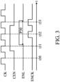
- FIG. 3 shows a timing chart of the signals of clock gating cell 1.
- the enable signal ENL in response to the falling edge of the clock signal CK at the time point t30, the enable signal ENL is at a low voltage level because the clock enable signal CEN is at a low voltage level at the time point t30.
- the clock enable signal CEN is switched to a high voltage level (that is, the clock enable signal CEN is asserted).
- the enable signal ENL is switched to a high voltage level (that is, the enable signal ENL is asserted) due to the high voltage level of the clock enable signal CEN.
- the enable signal ENL is maintained at the high voltage level because the clock enable signal CEN is still at the high voltage level at the time point t32.
- the clock enable signal CK is switched to the low voltage level.
- the enable signal ENL is switched to the low voltage level due to the low voltage level of the clock enable signal CEN.
- the clock enable signal CEN is latched in response to the falling edges of the clock signal CK to generate the enable signal ENL that is asserted (high voltage level) during the period P30.
- the output stage 11 comprises an AND gate circuit 21.
- the AND gate circuit 21 receives the enable signal ENL and the clock signal CK and generates the clock gating signal ENCK which corresponds to the clock signal CK in the asserted period P30 of the enable signal ENL.
- the AND gate circuit 21 is implemented by an AND logic gate 210.
- One input terminal of the AND logic gate 210 receives the enable signal ENL, the other input terminal thereof receives the clock signal CK, and an output terminal generating the clock gating signal ENCK.
- the clock gating signal ENCK varies with the clock signal CK during the asserted period P30 of the enable signal ENL, as shown in FIG.
- the clock gating signal ENCK corresponds to the clock signal CK during the asserted period P30 of the enable signal ENL. Referring to FIG. 3 , there are two pulses on the clock gating signal ENCK during the asserted period P30. Except these two pulse, the clock gating signal ENCK is maintained at the low voltage level, thereby achieving the clock gating operation of the clock gating cell.
- the latch circuit 20 in the input stage 10 operates based on the voltage threshold VT1, while the AND gate circuit 21 in the output stage 11 operates based on the voltage threshold VT2.
- the D latch 200 operates based on the voltage threshold VT1, while the AND logic gate 210 operates based on the voltage threshold VT2.
- the AND gate circuit 21 is implemented by a NAND logic gate 211 and an inverter 212, as shown in FIG. 2B .
- One input terminal of the NAND logic gate 211 receives the clock signal CK, and the other input terminal thereof receives the enable ENL.
- the input terminal of the inverter 212 is coupled to the output terminal of the NAND logic gate 211, and an output terminal thereof outputs the clock gating signal ENCK.
- the above operation of the AND gate circuit 21 implemented by the AND logic gate 210 can be achieved through the NAND logic gate 211 and the inverter 212.
- the NAND logic gate 211 and the inverter 212 operate based on the voltage threshold VT2.
- the clock gating cell 1 may receive two different input enable signals.
- the clock gating cell 1 receives both of the clock enable signal CEN and the testing enable signal TEN.
- the clock enable signal CEN and the testing enable signal TEN are not asserted at the same time.
- the latch circuit 20 further comprises a selector 40 as shown in FIG. 4 .
- the selector 40 selects one of the clock enable signal CEN and the testing enable signal TEN to serve as an enable signal S40 that is output to the data input terminal (D) of the D latch 200.
- the selector 40 is implemented by an OR logic gate 401.
- One input terminal of the OR logic gate 401 receives the testing enable signal TEN, and the other input terminal thereof receives the clock enable signal CEN.
- the enable signal S40 is generated at the output terminal of the OR logic gate 401. Based on the logic operation of the OR logic gate 401, when one of the clock enable signal CEN and the testing enable signal TEN is asserted (high voltage level), the enable signal S40 is asserted (high voltage level) with the asserted clock enable signal CEN or testing enable signal TEN. Thus, equivalently, the asserted clock enable signal CEN or testing enable signal TEN is selected to be output to the D latch 200.
- the D latch 200 and the AND logic gate 210 operate according to the enable signal S40 and the clock signal CK.
- the operations of the D latch 200 and the AND logic gate 210 when the clock enable signal CEN is asserted are the same as the operations described in the embodiment of FIG. 2A , and the operations thereof when the testing enable signal TEN is asserted are also the same as the operations described in the embodiment of FIG. 2A . Thus, the related description is omitted here.
- the selector 40 operates based on the voltage threshold VT1.
- the OR gate 401 operates based on the voltage threshold VT1.
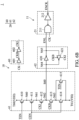
- the AND gate circuit 21 in the embodiment of FIG. 4A can be also implemented by a NAND logic gate 211 and an inverter 212, as shown in FIG. 4B .
- the connection and operations of the NAND logic gate 211 and the inverter 212 are the same as the embodiment of FIG. 2B . Thus, the related description is omitted here.
- the NAND logic gate 211 and the inverter 212 operate based on the voltage threshold VT2.
- FIG. 6A shows another exemplary embodiment of the clock gating cell 1.
- the clock gating cell 1 receives a clock enable signal CEN, a testing enable signal TEN, and a clock signal CK.
- the latch circuit 20 of the input stage 10 is implemented by an inverting circuit 60, a sampling circuit 61, and a holding circuit 62.
- the inverting circuit 60 comprises inverters 601 and 602.
- the inverter 601 receives the clock signal CK and inverts the clock signal CK to generate a clock signal CKB.
- the inverter 602 receives the clock signal CKB and inverts the clock signal CKB to generate a clock signal CKI.
- the sampling circuit 61 comprises P-type transistors 610-612 and N-type transistors 613-615.
- the P-type transistors 610-612 are implemented by P-type metal-oxide-semiconductor (PMOS) transistors
- the N-type transistors 613-615 are implemented by N-type metal-oxide-semiconductor (NMOS) transistors.
- the source of the PMOS transistor 610 is coupled to a voltage terminal T60, the drain thereof is coupled to a node N60, and the gate thereof receives the testing enable signal TEN.
- the source of the PMOS transistor 611 is coupled to the node N60, the drain thereof is coupled to a node N61, and the gate thereof receives the clock enable signal CEN.
- the source of the PMOS transistor 612 is coupled to the node N61, the drain thereof is coupled to a node N62, and the gate thereof receives the clock signal CKI.
- the drain of the NMOS transistor 613 is coupled to the node N62, the source thereof is coupled to a node N63, and the gate thereof receives the clock signal CKB.
- the drain of the NMOS transistor 614 is coupled to the node N63, the source thereof is coupled to a voltage terminal T61, and the gate thereof receives the clock enable signal CEN.
- the drain of the NMOS transistor 615 is coupled to the node N63, the source thereof is coupled to a voltage terminal T61, and the gate thereof receives the testing enable signal TEN.
- the PMOS transistor 610 and the NMOS transistor 615 are controlled by the testing enable signal TEN
- the PMOS transistor 611 and the NMOS transistor 614 are controlled by the clock enable signal CEN
- the PMOS transistor 612 is controlled by the clock signal CKI
- the NMOS transistor 613 is controlled by the clock signal CKB.
- An enable signal S60 is generated at the node 62.
- the holding circuit 62 has an input node N64 coupled to the sampling circuit 61.
- the input node N64 of the holding circuit 62 is coupled to the node N62 to receive the enable signal S60.
- the output node N65 of the holding circuit 62 is coupled to the AND gate circuit 21 of the output stage 11.
- the holding circuit 62 comprises inverters 620 and 621.
- the input terminal of the inverter 620 is coupled to the input node N64 to receive the enable signal S60, and the output terminal thereof is coupled to the output node N65.
- the input terminal of the inverter 621 is coupled to the output node N65, and the output terminal thereof is coupled to the output node N64.
- the inverter 621 further receives the clock signals CKB and CKI.
- the inverter 621 is controlled by the clock signals CKB and CKI. In the embodiment, whether the inverter 621 is enabled is determined according to the clock signals CKB and CKI.
- An enable signal ENL is generated at the output no
- the AND logic gate 210 of the output stage 11 receives the enable signal ENL and the clock signal CK.
- the AND logic gate 210 is implemented by an AND logic gate 210.
- One input terminal of the AND logic gate 210 receives the enable signal ENL, the other input terminal thereof receives the clock signal CK, and an output terminal generating the clock gating signal ENCK.
- the voltage terminal T60 receives an operation voltage VDD with a high level, while the voltage terminal T61 receives an operation voltage VSS with a low level.
- the clock signal CK when a falling edge of the clock signal CK occurs at the time point at which both of the testing enable signal TEN and the clock enable signal CEN are de-asserted (low voltage level), for example, when a falling edge of the clock signal CK occurs at the time point t30, the PMOS transistors 610-612 and the NMOS transistor 613 are turned on, and the and NMOS transistors 614 and 615 are turned off.
- the enable signal S60 is at a high voltage level according to the operation voltage VDD.
- the inverter 620 generates the enable signal ENL with a low voltage level.
- the clock gating signal ENCK generated by the AND logic gate 210 is at a low voltage level based on the logic operation of the AND logic gate 210.
- the inverter 621 is disabled by the clock signals CKB and CKI.
- the holding operation of the holding circuit 62 is disabled, and the holding circuit 62 provides the inverting operation on the enable signal S60.
- the holding circuit 62 performs the holding operation through the inventers 620 and 621 to hold the low voltage level of the enable signal ENL.
- the clock enable signal CEN is switched to a high voltage level, that is, the clock enable signal CEN is asserted.
- the testing enable signal TEN is at the low voltage level continuously.
- the next falling edge of the clock signal CK occurs at the time point t31.
- the PMOS transistors 610 and 612 and the NMOS transistor 613 and 614 are turned on, and the PMOS transistor 611 and NMOS transistor 615 are turned off.
- the enable signal S60 is switched to a low voltage level (that is, the enable signal S60 is asserted) according to the operation voltage VSS.
- the inverter 620 generates the enable signal ENL with a high voltage level (that is, the enable signal ENL is asserted). Due to the high voltage level of the enable signal ENL, the clock gating signal ENCK generated by the AND logic gate 210 is maintained at the low voltage level in response to the falling edge of the clock signal CK.
- the inverter 621 is disabled by the clock signals CKB and CKI, and thus, the holding operation of the holding circuit 62 is disabled.
- the next rising edge occurs on the clock signal CK.
- Each of the PMOS transistor 612 and the NMOS transistor 613 is switched to the turned-off state.
- the inverter 621 is enabled by the clock signals CKB and CKI.
- the holding circuit 62 performs the holding operation through the inventers 620 and 621 to hold the high voltage level of the enable signal ENL. Due to the high voltage level of the enable signal ENL, the clock gating signal ENCK generated by the AND logic gate 210 is switched to a high voltage level in response to the rising edge of the clock signal CK.
- the enable signal S60 is maintained at the low voltage level according to the operation voltage VSS.
- the inverter 620 generates the enable signal ENL with the high voltage level.
- the inverter 621 is disabled by the clock signals CKB and CKI. Due to the high voltage level of the enable signal ENL, the clock gating signal ENCK generated by the AND logic gate 210 is switched to the low voltage level in response to the falling edge of the clock signal CK. In response to the falling edge of the clock signal at the time point t32, the inverter 621 is disabled by the clock signals CKB and CKI.
- the holding circuit 62 performs the holding operation through the inventers 620 and 621 to hold the high voltage level of the enable signal ENL. Due to the high voltage level of the enable signal ENL, the clock gating signal ENCK generated by the AND logic gate 210 is switched to the high voltage level in response to the rising edge of the clock signal CK.
- the clock enable signal CEN is switched to the low voltage level (that is, the clock enable signal CEN is de-asserted).
- the enable signal S60 is switched to the high voltage level (that is, the enable signal S60 is de-asserted) according to the operation voltage VDD.
- the inverter 620 generates the enable signal ENL with the low voltage level. Due to the low voltage level of the enable signal ENL, the clock gating signal ENCK generated by the AND logic gate 210 is switched to the low voltage level based on the logic operation of the AND logic gate 210.
- the clock gating signal ENCK corresponds to the clock signal CK during the asserted period (high voltage level) of the enable signal ENL. Except these two pulse, the clock gating signal ENCK is maintained at the low voltage level, thereby achieving the clock gating operation of the clock gating cell.
- the clock enable signal CEN When the clock enable signal CEN is asserted again or the testing enable signal is asserted, at least one pulse occurs on the clock gating signal ENCK in response to at least one falling edge of the clock signal CK during the asserted period of the enable signal ENL.
- the testing enable signal when the testing enable signal is asserted, two pulses occurs on the clock gating signal ENCK in response to two falling edges of the clock signal CK during the asserted period of the enable signal ENL.
- the operations of the inverting circuit 60, the sampling circuit 61, the holding circuit 62, and the AND gate circuit 21 are similar to those for the asserted clock enable signal CEN as described above. Thus, the related description is omitted here.
- the inverting circuit 60, the sampling circuit 61, the holding circuit 62 operate based on the voltage threshold VT1, while the AND gate circuit 21 operates based on the voltage threshold VT2.
- the devices 601, 602, 610-615, 620, and 621 operate based on the voltage threshold VT1, while the AND logic gate 210 operates based on the voltage threshold VT2
- the AND gate circuit 21 in the embodiment of FIG. 6A is implemented by a NAND logic gate 211 and an inverter 212, as shown in FIG. 6B .
- the connection and operations of the NAND logic gate 211 and the inverter 212 are the same as the embodiment of FIG. 2B . Thus, the related description is omitted here.
- the NAND logic gate 211 and the inverter 212 operate based on the voltage threshold VT2.
- FIG. 7 shows another exemplary embodiment of the clock gating cell 1.
- the input stage 10 comprises a latch circuit 70
- the output stage 11 comprises a NOR logic gate 71.
- the latch circuit 70 receives a clock enable signal CEN or a testing enable signal TEN and further receives a clock signal CK.
- the latch circuit 70 latches the received clock enable signal CEN or testing enable signal TEN in response to the falling edges of the clock signal CK to generate an enable signal ENL70.
- One input terminal of the NOR logic gate 71 receives the enable signal ENL70, and the other input terminal thereof receives the clock signal CK.
- the NOR logic gate 71 generates a clock gating signal ENCK70 at the output terminal of the NOR logic gate 71 according to the enable signal 70 and the clock signal CK. Through the operations of the latch circuit 70 and the NOR logic gate 71, the clock gating operation is achieved.
- the latch circuit 70 in the input stage 10 operates based on the voltage threshold VT1, while the NOR gate circuit 71 in the output stage 11 operates based on the voltage threshold VT2.
- the voltage threshold VT1 is greater than the voltage threshold VT2.
- the voltage threshold VT2 is greater than the voltage threshold VT1.
- the magnitude relationship between the voltage threshold VT1 and VT2 is determined according to requirements or specifications of system or hardware designs.
- a clock gating cell operates based on multiple voltage thresholds.
- the clock gating cell is divided two portions: an input stage and an output stage. One of the two stages operates based on a high voltage threshold, while the other one of the two stages operates on a low voltage threshold.
- a clock tree comprises clock gating cells, each of which has different voltage thresholds, the better performance of the clock tree can be achieved. Moreover, the leakage current of the clock tree is reduced, which causes less power consumption.
Landscapes
- Engineering & Computer Science (AREA)
- Physics & Mathematics (AREA)
- General Engineering & Computer Science (AREA)
- Theoretical Computer Science (AREA)
- Computer Hardware Design (AREA)
- Computing Systems (AREA)
- Mathematical Physics (AREA)
- General Physics & Mathematics (AREA)
- Power Engineering (AREA)
- Manipulation Of Pulses (AREA)
- Logic Circuits (AREA)
Abstract
Description
- The invention relates to a clock gating cell, and more particularly to a low power clock gating cell.
- A clock tree is a clock distribution network within a system or hardware design. A clock tree comprises a clock source, clock cells (such as buffers or inverters), and clock gating cells. These components are connected to form clock branches to provide various clock signals. Generally, within a clock tree, each clock gating cell operates based on a single voltage threshold. In other words, all the devices in one clock gating cell operate based on the same voltage threshold. For example, each clock gating cell within a clock tree operates based on a low voltage threshold so that the clock tree performs better. However, a clock gate cell with a low voltage threshold may induce a larger leakage current, which causes high power consumption.
- Thus, the present invention provides a low power clock gating cell which operate based on multiple voltage thresholds, which reduces the leakage current.
- An exemplary embodiment of a clock gating cell. The clock gating cell comprises an input stage and an output stage. The input stage receives a first clock signal and at least one input enable signal and generates a first enable signal corresponding to one of the least one input enable signal according to the first clock signal. The output stage is coupled to the input stage. The output stage receives the first enable signal and the first clock signal and generates a clock gating signal according to the first enable signal and the first clock signal. The input stage operates based on a first voltage threshold, and the output stage operates based on a second voltage threshold. The first voltage threshold is different from the second voltage threshold.
- In one embodiment, the first voltage threshold is greater than the second voltage threshold. In another embodiment, the second voltage threshold is greater than the first voltage threshold.
- A detailed description is given in the following embodiments with reference to the accompanying drawings.
- The invention can be more fully understood by reading the subsequent detailed description and examples with references made to the accompanying drawings, wherein:
-
FIG. 1 shows one exemplary embodiment of a clock gating cell; -
FIG. 2A shows another exemplary embodiment of a clock gating cell; -
FIG. 2B shows another exemplary embodiment of a clock gating cell; -
FIG. 3 shows a timing chart of signals of a clock gating cell according to one exemplary embodiment; -
FIG. 4A shows another exemplary embodiment of a clock gating cell; -
FIG. 4B shows another exemplary embodiment of a clock gating cell; -
FIG. 5 shows a timing chart of signals of a clock gating cell according to another exemplary embodiment; -
FIG. 6A shows another exemplary embodiment of a clock gating cell; -
FIG. 6B shows another exemplary embodiment of a clock gating cell; and -
FIG. 7 shows another exemplary embodiment of a clock gating cell. - The following description is of the best-contemplated mode of carrying out the invention. This description is made for the purpose of illustrating the general principles of the invention and should not be taken in a limiting sense. The scope of the invention is best determined by reference to the appended claims.
-
FIG. 1 shows an exemplary embodiment of a clock gating cell. As shown inFIG. 1 , aclock gating cell 1 comprises aninput stage 10 and anoutput stage 11. In an embodiment, a clock tree comprises a plurality ofclock gating cell 1. For example, at least one clock gating cell is used in each branch of the clock tree. Theinput stage 10 operates based on a voltage threshold VT1, while theoutput stage 11 operates based on a voltage threshold VT2. The voltage threshold VT1 is different from the voltage threshold VT2. In one embodiment, the voltage threshold VT1 is greater than the voltage threshold VT2. In another embodiment, the voltage threshold VT2 is greater than the voltage threshold VT1. The magnitude relationship between the voltage thresholds VT1 and VT2 is determined according to the requirements or specifications of system or hardware designs. - Referring to
FIG. 1 , theclock gating cell 1 receives an input enable signal and a clock signal CK and generates a clock gating signal ENCK. The input enable signal may be a clock enable signal CEN or a testing enable signal TEN. In an embodiment, the testing enable signal TEN may be a signal for enabling a testing mode, for example, a scan testing mode for detecting faults occurring in a combinational logic circuit associated with the clock gating cell. The clock enable signal CEN may be a signal for enabling the transmission of the clock signal CK, for example, in a normal operation. - In the embodiment of
FIG. 1 , theclock gating cell 1 receiving the clock enable signal CEN as the input enable signal is taken as an example for explaining the operation of theclock gating cell 1. Theinput stage 10 receives the clock signal CK and the clock enable signal CEN. Theinput stage 10 latches the clock enable signal CEN according to the clock signal CK to generate an enable signal ENL. For example, in response to each falling edge of the clock signal CK, the voltage level of the clock enable CEN is sampled, and theinput stage 10 generates the enable signal ENL with the sample voltage level. Theoutput stage 11 is coupled to theinput stage 10 to receive the enable signal ENL. Theoutput stage 11 further receives the clock signal CK. Theoutput stage 11 generates a clock gating signal ENCK according to the enable signal ENL and the clock signal CK. The clock gating signal ENCK corresponds to the clock signal CK in an asserted period of the ENL enable signal. Thus, the clock gating operation is achieved. -
FIG. 2A shows another exemplary embodiment of a clock gating cell. Referring toFIG. 2A , theinput stage 10 comprises alatch circuit 20, and theoutput stage 11 comprises an ANDgate circuit 21. Thelatch circuit 20 receives the clock enable signal CEN and the clock signal CK and latches the clock enable signal CEN in response to the rising or falling edges of the clock signal CK to generate the enable signal ENL. In the embodiment ofFIG. 2A , thelatch circuit 20 is implemented by aD latch 200. TheD latch 200 has a data input terminal (D) receiving the clock enable signal CEN, a clock input terminal receiving the clock signal CK, and an output terminal (Q) outputting the enable signal ENL. TheD latch 200 is triggered by the falling edges of the clock signal CK. In response to each falling edge of the clock signal CK, the enable signal ENL generated at the output terminal (Q) has the same voltage level as the clock enable signal CEN, thereby latching the clock enable signal CEN in response to the falling edges of the clock signal CK. -
FIG. 3 shows a timing chart of the signals ofclock gating cell 1. Referring toFIGs. 2A and3 , in response to the falling edge of the clock signal CK at the time point t30, the enable signal ENL is at a low voltage level because the clock enable signal CEN is at a low voltage level at the time point t30. After the time point t30, the clock enable signal CEN is switched to a high voltage level (that is, the clock enable signal CEN is asserted). In response to the falling edge of the clock signal CK at the time point t31, the enable signal ENL is switched to a high voltage level (that is, the enable signal ENL is asserted) due to the high voltage level of the clock enable signal CEN. In response to the falling edge of the clock signal CK at the time point t32, the enable signal ENL is maintained at the high voltage level because the clock enable signal CEN is still at the high voltage level at the time point t32. After the time point t32, the clock enable signal CK is switched to the low voltage level. Then, in response to the falling edge of the clock signal CK at the time point t33, the enable signal ENL is switched to the low voltage level due to the low voltage level of the clock enable signal CEN. Through the operation of theD latch 200, the clock enable signal CEN is latched in response to the falling edges of the clock signal CK to generate the enable signal ENL that is asserted (high voltage level) during the period P30. - Referring to
FIG. 2A , theoutput stage 11 comprises an ANDgate circuit 21. The ANDgate circuit 21 receives the enable signal ENL and the clock signal CK and generates the clock gating signal ENCK which corresponds to the clock signal CK in the asserted period P30 of the enable signal ENL. In the embodiment ofFIG. 2A , the ANDgate circuit 21 is implemented by an ANDlogic gate 210. One input terminal of the ANDlogic gate 210 receives the enable signal ENL, the other input terminal thereof receives the clock signal CK, and an output terminal generating the clock gating signal ENCK. Based on the operation of the ANDlogic gate 210, the clock gating signal ENCK varies with the clock signal CK during the asserted period P30 of the enable signal ENL, as shown in FIG. 3A. The clock gating signal ENCK corresponds to the clock signal CK during the asserted period P30 of the enable signal ENL. Referring toFIG. 3 , there are two pulses on the clock gating signal ENCK during the asserted period P30. Except these two pulse, the clock gating signal ENCK is maintained at the low voltage level, thereby achieving the clock gating operation of the clock gating cell. - In the embodiment of
FIG. 2A , thelatch circuit 20 in theinput stage 10 operates based on the voltage threshold VT1, while the ANDgate circuit 21 in theoutput stage 11 operates based on the voltage threshold VT2. In details, theD latch 200 operates based on the voltage threshold VT1, while the ANDlogic gate 210 operates based on the voltage threshold VT2. - In another embodiment, the AND
gate circuit 21 is implemented by aNAND logic gate 211 and aninverter 212, as shown inFIG. 2B . One input terminal of theNAND logic gate 211 receives the clock signal CK, and the other input terminal thereof receives the enable ENL. The input terminal of theinverter 212 is coupled to the output terminal of theNAND logic gate 211, and an output terminal thereof outputs the clock gating signal ENCK. Based on the logic operations of theNAND logic gate 211 and theinverter 212, the above operation of the ANDgate circuit 21 implemented by the ANDlogic gate 210 can be achieved through theNAND logic gate 211 and theinverter 212. In the embodiment ofFIG. 2B , theNAND logic gate 211 and theinverter 212 operate based on the voltage threshold VT2. - According to another embodiment, the
clock gating cell 1 may receive two different input enable signals. For example, theclock gating cell 1 receives both of the clock enable signal CEN and the testing enable signal TEN. Referring toFIG. 5 , the clock enable signal CEN and the testing enable signal TEN are not asserted at the same time. For the two different input enable signals (CEN and TEN), thelatch circuit 20 further comprises aselector 40 as shown inFIG. 4 . Theselector 40 selects one of the clock enable signal CEN and the testing enable signal TEN to serve as an enable signal S40 that is output to the data input terminal (D) of theD latch 200. In the embodiment ofFIG. 4A , theselector 40 is implemented by anOR logic gate 401. One input terminal of theOR logic gate 401 receives the testing enable signal TEN, and the other input terminal thereof receives the clock enable signal CEN. The enable signal S40 is generated at the output terminal of theOR logic gate 401. Based on the logic operation of theOR logic gate 401, when one of the clock enable signal CEN and the testing enable signal TEN is asserted (high voltage level), the enable signal S40 is asserted (high voltage level) with the asserted clock enable signal CEN or testing enable signal TEN. Thus, equivalently, the asserted clock enable signal CEN or testing enable signal TEN is selected to be output to theD latch 200. - The
D latch 200 and the ANDlogic gate 210 operate according to the enable signal S40 and the clock signal CK. The operations of theD latch 200 and the ANDlogic gate 210 when the clock enable signal CEN is asserted are the same as the operations described in the embodiment ofFIG. 2A , and the operations thereof when the testing enable signal TEN is asserted are also the same as the operations described in the embodiment ofFIG. 2A . Thus, the related description is omitted here. In the embodiment ofFIG. 4A , theselector 40 operates based on the voltage threshold VT1. In details, theOR gate 401 operates based on the voltage threshold VT1. - In another embodiment, the AND
gate circuit 21 in the embodiment ofFIG. 4A can be also implemented by aNAND logic gate 211 and aninverter 212, as shown inFIG. 4B . The connection and operations of theNAND logic gate 211 and theinverter 212 are the same as the embodiment ofFIG. 2B . Thus, the related description is omitted here. In the embodiment ofFIG. 4B , theNAND logic gate 211 and theinverter 212 operate based on the voltage threshold VT2. -
FIG. 6A shows another exemplary embodiment of theclock gating cell 1. Theclock gating cell 1 receives a clock enable signal CEN, a testing enable signal TEN, and a clock signal CK. Referring toFIG. 6A , thelatch circuit 20 of theinput stage 10 is implemented by an invertingcircuit 60, asampling circuit 61, and a holdingcircuit 62. The invertingcircuit 60 comprisesinverters inverter 601 receives the clock signal CK and inverts the clock signal CK to generate a clock signal CKB. Then, theinverter 602 receives the clock signal CKB and inverts the clock signal CKB to generate a clock signal CKI. - As shown in
FIG. 6 , thesampling circuit 61 comprises P-type transistors 610-612 and N-type transistors 613-615. In the embodiment, the P-type transistors 610-612 are implemented by P-type metal-oxide-semiconductor (PMOS) transistors, and the N-type transistors 613-615 are implemented by N-type metal-oxide-semiconductor (NMOS) transistors. The source of thePMOS transistor 610 is coupled to a voltage terminal T60, the drain thereof is coupled to a node N60, and the gate thereof receives the testing enable signal TEN. The source of thePMOS transistor 611 is coupled to the node N60, the drain thereof is coupled to a node N61, and the gate thereof receives the clock enable signal CEN. The source of thePMOS transistor 612 is coupled to the node N61, the drain thereof is coupled to a node N62, and the gate thereof receives the clock signal CKI. The drain of theNMOS transistor 613 is coupled to the node N62, the source thereof is coupled to a node N63, and the gate thereof receives the clock signal CKB. The drain of theNMOS transistor 614 is coupled to the node N63, the source thereof is coupled to a voltage terminal T61, and the gate thereof receives the clock enable signal CEN. The drain of theNMOS transistor 615 is coupled to the node N63, the source thereof is coupled to a voltage terminal T61, and the gate thereof receives the testing enable signal TEN. According to the above connection of the transistors 610-615, thePMOS transistor 610 and theNMOS transistor 615 are controlled by the testing enable signal TEN, thePMOS transistor 611 and theNMOS transistor 614 are controlled by the clock enable signal CEN, thePMOS transistor 612 is controlled by the clock signal CKI, and theNMOS transistor 613 is controlled by the clock signal CKB. An enable signal S60 is generated at thenode 62. - The holding
circuit 62 has an input node N64 coupled to thesampling circuit 61. In details, the input node N64 of the holdingcircuit 62 is coupled to the node N62 to receive the enable signal S60. The output node N65 of the holdingcircuit 62 is coupled to the ANDgate circuit 21 of theoutput stage 11. The holdingcircuit 62 comprisesinverters inverter 620 is coupled to the input node N64 to receive the enable signal S60, and the output terminal thereof is coupled to the output node N65. The input terminal of theinverter 621 is coupled to the output node N65, and the output terminal thereof is coupled to the output node N64. Theinverter 621 further receives the clock signals CKB and CKI. Theinverter 621 is controlled by the clock signals CKB and CKI. In the embodiment, whether theinverter 621 is enabled is determined according to the clock signals CKB and CKI. An enable signal ENL is generated at the output node N65. - Referring to
FIG. 6A , the ANDlogic gate 210 of theoutput stage 11 receives the enable signal ENL and the clock signal CK. In the embodiment ofFIG. 6A , the ANDlogic gate 210 is implemented by an ANDlogic gate 210. One input terminal of the ANDlogic gate 210 receives the enable signal ENL, the other input terminal thereof receives the clock signal CK, and an output terminal generating the clock gating signal ENCK. - In the embodiment, the voltage terminal T60 receives an operation voltage VDD with a high level, while the voltage terminal T61 receives an operation voltage VSS with a low level.
- The operation of the
clock gating cell 1 in the embodiment ofFIG. 6A will be described in the following paragraphs. - Referring to
FIG. 5 and6A , when a falling edge of the clock signal CK occurs at the time point at which both of the testing enable signal TEN and the clock enable signal CEN are de-asserted (low voltage level), for example, when a falling edge of the clock signal CK occurs at the time point t30, the PMOS transistors 610-612 and theNMOS transistor 613 are turned on, and the andNMOS transistors inverter 620 generates the enable signal ENL with a low voltage level. Due to the low voltage level of the enable signal ENL, the clock gating signal ENCK generated by the ANDlogic gate 210 is at a low voltage level based on the logic operation of the ANDlogic gate 210. In response to the falling edge of the clock signal at the time point t30, theinverter 621 is disabled by the clock signals CKB and CKI. Thus, the holding operation of the holdingcircuit 62 is disabled, and the holdingcircuit 62 provides the inverting operation on the enable signal S60. - At the time t60, there is a rising edge on the clock signal CK. Each of the
PMOS transistor 612 and theNMOS transistor 613 is switched to a turned-off state. Theinverter 621 is enabled by the clock signals CKB and CKI. Thus, the holdingcircuit 62 performs the holding operation through theinventers - After the time point t60, the clock enable signal CEN is switched to a high voltage level, that is, the clock enable signal CEN is asserted. The testing enable signal TEN is at the low voltage level continuously.
- The next falling edge of the clock signal CK occurs at the time point t31. The
PMOS transistors NMOS transistor PMOS transistor 611 andNMOS transistor 615 are turned off. The enable signal S60 is switched to a low voltage level (that is, the enable signal S60 is asserted) according to the operation voltage VSS. Theinverter 620 generates the enable signal ENL with a high voltage level (that is, the enable signal ENL is asserted). Due to the high voltage level of the enable signal ENL, the clock gating signal ENCK generated by the ANDlogic gate 210 is maintained at the low voltage level in response to the falling edge of the clock signal CK. In response to the falling edge of the clock signal at the time point t31, theinverter 621 is disabled by the clock signals CKB and CKI, and thus, the holding operation of the holdingcircuit 62 is disabled. - At the time t61, the next rising edge occurs on the clock signal CK. Each of the
PMOS transistor 612 and theNMOS transistor 613 is switched to the turned-off state. Theinverter 621 is enabled by the clock signals CKB and CKI. Thus, the holdingcircuit 62 performs the holding operation through theinventers logic gate 210 is switched to a high voltage level in response to the rising edge of the clock signal CK. - Then, another falling edge of the clock signal CK occurs at the time point t32. The
PMOS transistors NMOS transistor PMOS transistor 611 andNMOS transistor 615 are turned off. The enable signal S60 is maintained at the low voltage level according to the operation voltage VSS. Theinverter 620 generates the enable signal ENL with the high voltage level. Theinverter 621 is disabled by the clock signals CKB and CKI. Due to the high voltage level of the enable signal ENL, the clock gating signal ENCK generated by the ANDlogic gate 210 is switched to the low voltage level in response to the falling edge of the clock signal CK. In response to the falling edge of the clock signal at the time point t32, theinverter 621 is disabled by the clock signals CKB and CKI. - At the time t62, another rising edge occurs on the clock signal CK. Each of the
PMOS transistor 612 and theNMOS transistor 613 is switched to the turned-off state. Theinverter 621 is enabled by the clock signals CKB and CKI. Thus, the holdingcircuit 62 performs the holding operation through theinventers logic gate 210 is switched to the high voltage level in response to the rising edge of the clock signal CK. - After the time point t62, the clock enable signal CEN is switched to the low voltage level (that is, the clock enable signal CEN is de-asserted).
- At the time point t33, another falling edge of the clock signal CK occurs. The PMOS transistors 610-612 and the
NMOS transistor 613 are turned on, andNMOS transistors inverter 620 generates the enable signal ENL with the low voltage level. Due to the low voltage level of the enable signal ENL, the clock gating signal ENCK generated by the ANDlogic gate 210 is switched to the low voltage level based on the logic operation of the ANDlogic gate 210. - According to the above operation, the clock gating signal ENCK corresponds to the clock signal CK during the asserted period (high voltage level) of the enable signal ENL. Except these two pulse, the clock gating signal ENCK is maintained at the low voltage level, thereby achieving the clock gating operation of the clock gating cell.
- When the clock enable signal CEN is asserted again or the testing enable signal is asserted, at least one pulse occurs on the clock gating signal ENCK in response to at least one falling edge of the clock signal CK during the asserted period of the enable signal ENL. For example, referring to
FIG. 5 , when the testing enable signal is asserted, two pulses occurs on the clock gating signal ENCK in response to two falling edges of the clock signal CK during the asserted period of the enable signal ENL. The operations of the invertingcircuit 60, thesampling circuit 61, the holdingcircuit 62, and the ANDgate circuit 21 are similar to those for the asserted clock enable signal CEN as described above. Thus, the related description is omitted here. - In the embodiment of
FIG. 6A , the invertingcircuit 60, thesampling circuit 61, the holdingcircuit 62 operate based on the voltage threshold VT1, while the ANDgate circuit 21 operates based on the voltage threshold VT2. In details, thedevices logic gate 210 operates based on the voltage threshold VT2 - In another embodiment, the AND
gate circuit 21 in the embodiment ofFIG. 6A is implemented by aNAND logic gate 211 and aninverter 212, as shown inFIG. 6B . The connection and operations of theNAND logic gate 211 and theinverter 212 are the same as the embodiment ofFIG. 2B . Thus, the related description is omitted here. In the embodiment ofFIG. 6B , theNAND logic gate 211 and theinverter 212 operate based on the voltage threshold VT2. -
FIG. 7 shows another exemplary embodiment of theclock gating cell 1. Referring toFIG. 7 , theinput stage 10 comprises alatch circuit 70, and theoutput stage 11 comprises a NORlogic gate 71. Thelatch circuit 70 receives a clock enable signal CEN or a testing enable signal TEN and further receives a clock signal CK. Thelatch circuit 70 latches the received clock enable signal CEN or testing enable signal TEN in response to the falling edges of the clock signal CK to generate an enable signal ENL70. One input terminal of the NORlogic gate 71 receives the enable signal ENL70, and the other input terminal thereof receives the clock signal CK. The NORlogic gate 71 generates a clock gating signal ENCK70 at the output terminal of the NORlogic gate 71 according to the enablesignal 70 and the clock signal CK. Through the operations of thelatch circuit 70 and the NORlogic gate 71, the clock gating operation is achieved. - In the embodiment of
FIG. 7 , thelatch circuit 70 in theinput stage 10 operates based on the voltage threshold VT1, while the NORgate circuit 71 in theoutput stage 11 operates based on the voltage threshold VT2. In one embodiment, the voltage threshold VT1 is greater than the voltage threshold VT2. In another embodiment, the voltage threshold VT2 is greater than the voltage threshold VT1. The magnitude relationship between the voltage threshold VT1 and VT2 is determined according to requirements or specifications of system or hardware designs. - According to the above embodiments, a clock gating cell operates based on multiple voltage thresholds. The clock gating cell is divided two portions: an input stage and an output stage. One of the two stages operates based on a high voltage threshold, while the other one of the two stages operates on a low voltage threshold. When a clock tree comprises clock gating cells, each of which has different voltage thresholds, the better performance of the clock tree can be achieved. Moreover, the leakage current of the clock tree is reduced, which causes less power consumption.
- While the invention has been described by way of example and in terms of the preferred embodiments, it is to be understood that the invention is not limited to the disclosed embodiments. To the contrary, it is intended to cover various modifications and similar arrangements (as would be apparent to those skilled in the art). Therefore, the scope of the appended claims should be accorded the broadest interpretation so as to encompass all such modifications and similar arrangements.
Claims (14)
- A clock gating cell comprising:an input stage receiving a first clock signal and at least one input enable signal and generating a first enable signal corresponding to one of the least one input enable signal according to the first clock signal; andan output stage, coupled to the input stage, receiving the first enable signal and the first clock signal and generating a clock gating signal according to the first enable signal and the first clock signal,wherein the input stage operates based on a first voltage threshold, and the output stage operates based on a second voltage threshold, andwherein the first voltage threshold is different from the second voltage threshold.
- The clock gating cell as claimed in claim 1, wherein:the at least one input enable signal comprises only one input enable signal;the input stage comprises a latch circuit, and the latch circuit receives the one input enable signal and the first clock signal and latches the one input enable signal in response to rising or falling edges of the first clock signal to generate the first enable signal, andthe output stage comprises an AND gate circuit, and the AND gate circuit receives the first enable signal and the first clock signal and generates the clock gating signal which corresponds to the first clock signal in an asserted period of the first enable signal.
- The clock gating cell as claimed in claim 2, wherein the latch circuit operates based on the first voltage threshold, and the AND gate circuit operates based on the second voltage threshold.
- The clock gating cell as claimed in claim 2 or claim 3, wherein the output stage comprises:
an AND logic gate receiving the first clock signal and the first enable signal and generating the clock gating signal. - The clock gating cell as claimed in claim 2 or claim 3, wherein the output stage comprises:a NAND logic gate having a first input terminal receiving the first clock signal, a second input terminal receiving the first enable signal, and an output terminal;an inverter having an input terminal coupled to the output terminal of the NAND logic gate and an output terminal outputting the clock gating signal.
- The clock gating cell as claimed in any one of the preceding claims, wherein the at least one input enable signal comprises a testing enable signal and a clock enable signal, and the input stage comprises:a selector receiving the testing enable signal and the clock enable signal and selecting one of the testing enable signal and the clock enable signal to serve as a second enable signal,wherein the input stage generates the first enable signal corresponding to the second enable signal according to the first clock signal.
- The clock gating cell as claimed in claim 6, wherein:the input stage further comprises a latch circuit, and the latch circuit receives the second enable signal and the first clock signal and latches the second enable signal in response to rising or falling edges of the first clock signal to generate the first enable signal, andthe output stage comprises an AND gate circuit, and the AND gate circuit receives the second enable signal and the first clock signal and generates the clock gating signal which corresponds to the first clock signal in an asserted period of the second enable signal.
- The clock gating cell as claimed in claim 7, wherein the selector and the latch circuit operate based on the first voltage threshold, and the AND gate circuit operates based on the second voltage threshold.
- The clock gating cell as claimed in any one of the preceding claims, wherein the at least one input enable signal comprises a testing enable signal and a clock enable signal, and the input stage comprises:an inverting circuit receiving the first clock signal, generating a second clock signal inverse to the first clock signal, and further generating a third clock signal inverse to the second clock signal;a sampling circuit receiving the testing enable and the clock enable signal and controlled by the second clock signal and the third clock signal to generate a second enable signal, wherein in response to one of the testing enable and the clock enable signal being asserted, the second enable signal is asserted; anda holding circuit coupled to the sampling circuit to receive the second enable signal and generating the first enable signal according to the second enable signal, wherein the latch circuit is configured to hold a voltage level of the first enable signal.
- The clock gating cell as claimed in claim 9, wherein the sampling circuit comprises:a first P-type transistor coupled between a first voltage terminal and a first node and controlled by the testing enable signal;a second P-type transistor coupled between the first node and a second node and controlled by the clock enable signal;a third P-type transistor coupled between the second node and a third node and controlled by the third clock signal;a first N-type transistor coupled between the third node and a fourth node and controlled by the second clock signal;a second N-type transistor coupled between the fourth node and a second voltage terminal and controlled by the clock enable signal; anda third N-type-transistor coupled between the fourth node and the second voltage terminal and controlled by the testing enable signal.
- The clock gating cell as claimed in claim 9 or claim 10, wherein the latch circuit is coupled to the sampling circuit at an input node to receive the second enable signal and coupled to the output stage at an output node, and the holding circuit comprises:a first inverter having an input terminal coupled to the input node and an output terminal coupled to the output node; anda second inverter having an input terminal coupled to the output node and an output terminal coupled to the input node and controlled by the second clock signal and the third clock signal to be enabled or disabled,wherein in response to the second inverter being enabled, the latch circuit is enabled, andwherein the first enable signal is generated at the output node.
- The clock gating cell as claimed in any one of claims 9 to 11, wherein the inverting circuit, the sampling circuit, and the latch circuit operate based on the first voltage threshold.
- The clock gating cell as claimed in claim 1, wherein:the at least one input enable signal comprises only one input enable signal;the input stage comprises a latch circuit, and the latch circuit receives the input enable signal and the first clock signal and latches the input enable signal in response to rising or falling edges of the first clock signal to generate the first enable signal,the output stage comprises a NOR logic gate and the NOR logic gate receives the first enable signal and the first clock signal and generates the clock gating signal which corresponds to the first clock signal in an asserted period of the first enable signal.
- The clock gating cell as claimed in claim 13, wherein the latch circuit operates based on the first voltage threshold, and the NOR gate circuit operates based on the second voltage threshold.
Applications Claiming Priority (2)
| Application Number | Priority Date | Filing Date | Title |
|---|---|---|---|
| US202163286585P | 2021-12-07 | 2021-12-07 | |
| US18/054,032 US12081214B2 (en) | 2021-12-07 | 2022-11-09 | Clock gating cells |
Publications (1)
| Publication Number | Publication Date |
|---|---|
| EP4195506A1 true EP4195506A1 (en) | 2023-06-14 |
Family
ID=86283230
Family Applications (1)
| Application Number | Title | Priority Date | Filing Date |
|---|---|---|---|
| EP22210445.7A Pending EP4195506A1 (en) | 2021-12-07 | 2022-11-30 | Clock gating cells |
Country Status (4)
| Country | Link |
|---|---|
| US (1) | US12081214B2 (en) |
| EP (1) | EP4195506A1 (en) |
| CN (1) | CN116248111A (en) |
| TW (1) | TWI827389B (en) |
Families Citing this family (3)
| Publication number | Priority date | Publication date | Assignee | Title |
|---|---|---|---|---|
| JP2022073314A (en) * | 2020-10-30 | 2022-05-17 | ソニーセミコンダクタソリューションズ株式会社 | Combined logic circuit |
| CN116959519B (en) * | 2023-09-20 | 2023-12-15 | 深圳比特微电子科技有限公司 | Storage device, system on chip comprising same and computing device |
| CN120049877A (en) * | 2025-04-23 | 2025-05-27 | 中国人民解放军国防科技大学 | High-speed gate control unit circuit |
Citations (4)
| Publication number | Priority date | Publication date | Assignee | Title |
|---|---|---|---|---|
| US20080129359A1 (en) * | 2006-12-05 | 2008-06-05 | Dae Woo Lee | Low-power clock gating circuit |
| US20120286824A1 (en) * | 2011-05-13 | 2012-11-15 | Arm Limited | Supplying a clock signal and a gated clock signal to synchronous elements |
| US20160077544A1 (en) * | 2014-09-17 | 2016-03-17 | Taiwan Semiconductor Manufacturing Company, Ltd. | Clock gating circuits and circuit arrangements including clock gating circuits |
| WO2016114892A2 (en) * | 2015-01-15 | 2016-07-21 | Qualcomm Incorporated | Clock-gating cell with low area, low power, and low setup time |
Family Cites Families (6)
| Publication number | Priority date | Publication date | Assignee | Title |
|---|---|---|---|---|
| US7902878B2 (en) | 2008-04-29 | 2011-03-08 | Qualcomm Incorporated | Clock gating system and method |
| US10761559B2 (en) | 2016-12-13 | 2020-09-01 | Qualcomm Incorporated | Clock gating enable generation |
| US10409317B2 (en) * | 2017-06-05 | 2019-09-10 | Qualcomm Incorporated | Apparatus and methods for reducing clock-ungating induced voltage droop |
| US11244046B2 (en) | 2019-09-16 | 2022-02-08 | Nuvoton Technology Corporation | Data-sampling integrity check using gated clock |
| TWI730707B (en) * | 2020-04-01 | 2021-06-11 | 瑞昱半導體股份有限公司 | Clock gating cell |
| US11422819B2 (en) | 2020-06-12 | 2022-08-23 | Taiwan Semiconductor Manufacturing Company Limited | Power efficient multi-bit storage system |
-
2022
- 2022-11-09 US US18/054,032 patent/US12081214B2/en active Active
- 2022-11-30 EP EP22210445.7A patent/EP4195506A1/en active Pending
- 2022-12-06 CN CN202211559648.3A patent/CN116248111A/en active Pending
- 2022-12-07 TW TW111146945A patent/TWI827389B/en active
Patent Citations (4)
| Publication number | Priority date | Publication date | Assignee | Title |
|---|---|---|---|---|
| US20080129359A1 (en) * | 2006-12-05 | 2008-06-05 | Dae Woo Lee | Low-power clock gating circuit |
| US20120286824A1 (en) * | 2011-05-13 | 2012-11-15 | Arm Limited | Supplying a clock signal and a gated clock signal to synchronous elements |
| US20160077544A1 (en) * | 2014-09-17 | 2016-03-17 | Taiwan Semiconductor Manufacturing Company, Ltd. | Clock gating circuits and circuit arrangements including clock gating circuits |
| WO2016114892A2 (en) * | 2015-01-15 | 2016-07-21 | Qualcomm Incorporated | Clock-gating cell with low area, low power, and low setup time |
Also Published As
| Publication number | Publication date |
|---|---|
| US20230179206A1 (en) | 2023-06-08 |
| TWI827389B (en) | 2023-12-21 |
| CN116248111A (en) | 2023-06-09 |
| TW202324184A (en) | 2023-06-16 |
| US12081214B2 (en) | 2024-09-03 |
Similar Documents
| Publication | Publication Date | Title |
|---|---|---|
| US12081214B2 (en) | Clock gating cells | |
| US5867049A (en) | Zero setup time flip flop | |
| US9509317B2 (en) | Rotational synchronizer circuit for metastablity resolution | |
| US7843243B2 (en) | Flip-flop circuit, pipeline circuit including a flip-flop circuit, and method of operating a flip-flop circuit | |
| US7202724B2 (en) | Pulse-based flip-flop | |
| US8947146B2 (en) | Pulse-based flip flop | |
| US20030062939A1 (en) | High speed sampling receiver with reduced output impedance | |
| US9081061B1 (en) | Scan flip-flop | |
| US10355672B2 (en) | Semiconductor device with power gating scheme | |
| US6873183B1 (en) | Method and circuit for glitchless clock control | |
| US7843244B1 (en) | Low latency synchronizer circuit | |
| US7414449B2 (en) | Dynamic scannable latch and method of operation | |
| US7961009B2 (en) | Domino logic block having data holding function and domino logic including the domino logic block | |
| US7164293B2 (en) | Dynamic latch having integral logic function and method therefor | |
| US6708261B1 (en) | Multi-stage data buffers having efficient data transfer characteristics and methods of operating same | |
| US8432195B2 (en) | Latch circuits with synchronous data loading and self-timed asynchronous data capture | |
| US10706916B1 (en) | Method and apparatus for integrated level-shifter and memory clock | |
| US8248129B2 (en) | Signal delay circuit, clock transfer control circuit and semiconductor device having the same | |
| US6040719A (en) | Input receiver for limiting current during reliability screening | |
| US20120169382A1 (en) | Dividing method and dividing apparatus for generating noise-reduced frequency divided signal by utilizing noise reducing circuit | |
| KR100712986B1 (en) | Latch circuit | |
| KR100613458B1 (en) | Flip flop | |
| GB2440460A (en) | Fast dynamic CMOS flip-flops and gates | |
| KR100611309B1 (en) | Latch and Flip-Flop With The Same | |
| GB2437439A (en) | A pulse-type flip-flop using a latch with clocked inverters |
Legal Events
| Date | Code | Title | Description |
|---|---|---|---|
| PUAI | Public reference made under article 153(3) epc to a published international application that has entered the european phase |
Free format text: ORIGINAL CODE: 0009012 |
|
| STAA | Information on the status of an ep patent application or granted ep patent |
Free format text: STATUS: THE APPLICATION HAS BEEN PUBLISHED |
|
| AK | Designated contracting states |
Kind code of ref document: A1 Designated state(s): AL AT BE BG CH CY CZ DE DK EE ES FI FR GB GR HR HU IE IS IT LI LT LU LV MC ME MK MT NL NO PL PT RO RS SE SI SK SM TR |
|
| STAA | Information on the status of an ep patent application or granted ep patent |
Free format text: STATUS: REQUEST FOR EXAMINATION WAS MADE |
|
| 17P | Request for examination filed |
Effective date: 20231213 |
|
| RBV | Designated contracting states (corrected) |
Designated state(s): AL AT BE BG CH CY CZ DE DK EE ES FI FR GB GR HR HU IE IS IT LI LT LU LV MC ME MK MT NL NO PL PT RO RS SE SI SK SM TR |
|
| STAA | Information on the status of an ep patent application or granted ep patent |
Free format text: STATUS: EXAMINATION IS IN PROGRESS |
|
| 17Q | First examination report despatched |
Effective date: 20250326 |