EP4195402A1 - Rf component and method - Google Patents
Rf component and method Download PDFInfo
- Publication number
- EP4195402A1 EP4195402A1 EP21213985.1A EP21213985A EP4195402A1 EP 4195402 A1 EP4195402 A1 EP 4195402A1 EP 21213985 A EP21213985 A EP 21213985A EP 4195402 A1 EP4195402 A1 EP 4195402A1
- Authority
- EP
- European Patent Office
- Prior art keywords
- electrically conductive
- row
- signal
- conductive shielding
- component
- Prior art date
- Legal status (The legal status is an assumption and is not a legal conclusion. Google has not performed a legal analysis and makes no representation as to the accuracy of the status listed.)
- Granted
Links
Images



Classifications
-
- H—ELECTRICITY
- H05—ELECTRIC TECHNIQUES NOT OTHERWISE PROVIDED FOR
- H05K—PRINTED CIRCUITS; CASINGS OR CONSTRUCTIONAL DETAILS OF ELECTRIC APPARATUS; MANUFACTURE OF ASSEMBLAGES OF ELECTRICAL COMPONENTS
- H05K9/00—Screening of apparatus or components against electric or magnetic fields
-
- H—ELECTRICITY
- H01—ELECTRIC ELEMENTS
- H01P—WAVEGUIDES; RESONATORS, LINES, OR OTHER DEVICES OF THE WAVEGUIDE TYPE
- H01P1/00—Auxiliary devices
- H01P1/20—Frequency-selective devices, e.g. filters
- H01P1/2005—Electromagnetic photonic bandgaps [EPB], or photonic bandgaps [PBG]
-
- H—ELECTRICITY
- H05—ELECTRIC TECHNIQUES NOT OTHERWISE PROVIDED FOR
- H05K—PRINTED CIRCUITS; CASINGS OR CONSTRUCTIONAL DETAILS OF ELECTRIC APPARATUS; MANUFACTURE OF ASSEMBLAGES OF ELECTRICAL COMPONENTS
- H05K9/00—Screening of apparatus or components against electric or magnetic fields
- H05K9/0073—Shielding materials
- H05K9/0081—Electromagnetic shielding materials, e.g. EMI, RFI shielding
-
- H—ELECTRICITY
- H01—ELECTRIC ELEMENTS
- H01P—WAVEGUIDES; RESONATORS, LINES, OR OTHER DEVICES OF THE WAVEGUIDE TYPE
- H01P3/00—Waveguides; Transmission lines of the waveguide type
- H01P3/02—Waveguides; Transmission lines of the waveguide type with two longitudinal conductors
- H01P3/08—Microstrips; Strip lines
-
- H—ELECTRICITY
- H01—ELECTRIC ELEMENTS
- H01P—WAVEGUIDES; RESONATORS, LINES, OR OTHER DEVICES OF THE WAVEGUIDE TYPE
- H01P3/00—Waveguides; Transmission lines of the waveguide type
- H01P3/02—Waveguides; Transmission lines of the waveguide type with two longitudinal conductors
- H01P3/08—Microstrips; Strip lines
- H01P3/085—Triplate lines
-
- H—ELECTRICITY
- H01—ELECTRIC ELEMENTS
- H01Q—ANTENNAS, i.e. RADIO AERIALS
- H01Q1/00—Details of, or arrangements associated with, antennas
- H01Q1/52—Means for reducing coupling between antennas; Means for reducing coupling between an antenna and another structure
- H01Q1/526—Electromagnetic shields
-
- H—ELECTRICITY
- H05—ELECTRIC TECHNIQUES NOT OTHERWISE PROVIDED FOR
- H05K—PRINTED CIRCUITS; CASINGS OR CONSTRUCTIONAL DETAILS OF ELECTRIC APPARATUS; MANUFACTURE OF ASSEMBLAGES OF ELECTRICAL COMPONENTS
- H05K9/00—Screening of apparatus or components against electric or magnetic fields
- H05K9/0007—Casings
- H05K9/002—Casings with localised screening
- H05K9/0022—Casings with localised screening of components mounted on printed circuit boards [PCB]
- H05K9/0037—Housings with compartments containing a PCB, e.g. partitioning walls
-
- H—ELECTRICITY
- H10—SEMICONDUCTOR DEVICES; ELECTRIC SOLID-STATE DEVICES NOT OTHERWISE PROVIDED FOR
- H10W—GENERIC PACKAGES, INTERCONNECTIONS, CONNECTORS OR OTHER CONSTRUCTIONAL DETAILS OF DEVICES COVERED BY CLASS H10
- H10W42/00—Arrangements for protection of devices
- H10W42/20—Arrangements for protection of devices protecting against electromagnetic or particle radiation, e.g. light, X-rays, gamma-rays or electrons
-
- H—ELECTRICITY
- H10—SEMICONDUCTOR DEVICES; ELECTRIC SOLID-STATE DEVICES NOT OTHERWISE PROVIDED FOR
- H10W—GENERIC PACKAGES, INTERCONNECTIONS, CONNECTORS OR OTHER CONSTRUCTIONAL DETAILS OF DEVICES COVERED BY CLASS H10
- H10W44/00—Electrical arrangements for controlling or matching impedance
- H10W44/20—Electrical arrangements for controlling or matching impedance at high-frequency [HF] or radio frequency [RF]
Definitions
- the present specification relates to a Radio Frequency (RF) component and a method of making an RF component.
- RF Radio Frequency
- RF Radio Frequency
- RF Radio Frequency
- a barrier comprising rows of electrically conductive shielding members comprising polyhedra can provide greater design flexibility in customising the shape and configuration of the barrier for electromagnetically shielding the first and second electrically conductive signal members from each other.
- the use of polyhedra can also improve the electromagnetic isolation provided between the first and second electrically conductive signal members, particularly in combination with the offset provided between the first and second rows of electrically conductive shielding members.
- Each electrically conductive shielding member in each row may be elongate. This can further improve the isolation provided between the first and second electrically conductive signal members. For instance, the long dimension of each electrically conductive shielding member may be made greater than the gaps located between each electrically conductive shielding member in each row.
- a longitudinal axis of each polyhedron in each row may be substantially parallel to the longitudinal axis of that row. This can maximise the laterally facing profile of each electrically conductive shielding member in each row, again improving the isolation provided between the first and second electrically conductive signal members.
- the longitudinal axis of the first row may be substantially parallel to the longitudinal axis of the second row.
- Each electrically conductive shielding member in each row may be the same shape and size. This can make the shielding provided by the barrier more uniform along the length of the rows.
- the electrically conductive shielding members of the first row may be offset with respect to the electrically conductive shielding members of the second row such that a gap located between each electrically conductive shielding member of the first row is located opposite a middle of an electrically conductive shielding member of the second row. This can improve the isolation provided between the first and second electrically conductive signal members by increasing the path length for electromagnetic fields attempting to pass through the barrier.
- Each electrically conductive shielding member in each row may be a rectangular cuboid. This can simplify the manufacturing process.
- the electrically conductive shielding members of the rows of the barrier may collectively form a labyrinthine structure. This can improve the isolation provided between the first and second electrically conductive signal members by increasing the path length for electromagnetic fields attempting to pass through the barrier and by requiring the fields to navigate multiple (e.g. at least three, four, five or even more) turns within the barrier.
- Each electrically conductive shielding member of the first row may comprise:
- Each electrically conductive shielding member of the second row may comprise:
- a distal end of each arm of each electrically conductive shielding member of the first row may be located within a region located between the arms of an electrically conductive shielding member of the second row. This can force electromagnetic fields attempting to pass through the barrier to navigate additional turns within the barrier.
- a distal end of each arm of each electrically conductive shielding member of the second row may be located within a region located between the arms of an electrically conductive shielding member of the first row. This can force electromagnetic fields attempting to pass through the barrier to navigate additional turns within the barrier.
- the barrier may comprise at least one further row of electrically conductive shielding members spaced apart along a longitudinal axis of that further row.
- Each electrically conductive shielding member in the or each further row may comprise a polyhedron.
- the first electrically conductive signal member may comprise a transmission line.
- the second electrically conductive signal member may comprise a transmission line.
- the first electrically conductive signal member may comprise an antenna.
- the second electrically conductive signal member may comprise an antenna.
- a semiconductor device comprising a package containing an RF component of the kind set out above.
- Radio Frequency refers to a frequency in the range 300 GHz ⁇ f ⁇ 20 kHz.
- Figures 1 and 2 show an example of an RF component 10 including a first electrically conductive signal member 2 for conveying an RF signal and a second electrically conductive signal member 4 for conveying an RF signal.
- Figure 1 is a cross section of the RF component 10 through the longitudinal axes of the electrically conductive signal members 2, 4 (e.g. along the line A-A in Figure 2) and
- Figure 2 is a plan view of the RF component 10.
- the first and second electrically conductive signal members 2, 4 are transmission lines e.g. strip lines.
- the electrically conductive signal members 2, 4 could be other kinds of components, such as antennae.
- the first and second electrically conductive signal members 2, 4 may be provided in a laminated structure such as a metallization stack including a plurality of dielectric layers and layers of patterned metal features. Electrically conductive side walls 12, 16 may be provided at either lateral side of the RF component 10. Similarly, upper and lower electrically conductive walls 18 may be provided above and below the first and second electrically conductive signal members 2, 4. Each electrically conductive signal member 2, 4 may be located within a respective dielectric region 6, 8. The dielectric regions 6, 8 may be enclosed by the electrically conductive side walls 12, 16 and the upper and lower electrically conductive walls 18.
- the electrically conductive features, including the electrically conductive signal members 2, 4, the electrically conductive side walls 12, 16, the upper and lower electrically conductive walls 18 (and the barrier 14 to be described below) may be formed as the patterned metal features of the metallisation stack.
- the example shown in Figures 1 and 2 is provided with a barrier 14.
- the barrier 14 is electrically conductive (e.g. metallic) and is located between the first electrically conductive signal member 2 and the second electrically conductive signal member 4, and between the upper and lower electrically conductive walls 18.
- the side walls 12, 16, the first electrically conductive signal member 2, the second electrically conductive signal member 4 and the barrier 14 are elongate and coextend along a longitudinal axis of the RF component 10.
- the first electrically conductive signal member 2 and the second electrically conductive signal member 4 in this example form strip lines. It will be appreciated that the elongate, coextensive arrangement shown in Figure 2 is not essential, particularly, for example, where the electrically conductive signal members 2, 4 form RF components other than strip lines.
- the barrier 14 in this example is formed by a monolithic metallic block.
- the sidewalls 12, 16 in this example are also provided as monolithic blocks.
- the use of a barrier 14 comprising a monolithic block may be seen as the ideal case for the purposes of providing electromagnetic shielding between the first electrically conductive signal member 2 and the second electrically conductive signal member 4.
- the provision of a monolithic barrier 14 and side walls 12, 16 of the kind shown in Figures 1 and 2 is generally not possible, due to manufacturing constraints. For example, it is generally not possible to enclose the electrically conductive signal members 2, 4 completely within a monolithic wall, as there would be no way to allow the mold compound to evenly distribute during manufacture.
- Figure 3 shows another example of an RF component 10 including two strip lines 2, 4.
- the example shown in Figure 3 uses linear rows of electrically conductive vias instead of monolithic blocks for the side walls and barrier described above in relation to Figures 1 and 2 .
- a row of electrically conductive vias 22 forms the side wall 12
- a row of electrically conductive vias 26 forms the side wall 16
- one or more rows of electrically conductive vias 24A, 24B form the barrier 14.
- the vias 24A, 24B may comprise vias filled with electrically conductive material (e.g. metal) located within a metallization stack.
- the example shown in Figure 3 may also comprise upper and lower electrically conductive walls 18 of the kind shown in Figure 1 .
- the barrier in the example of Figure 3 provides a lower degree of electromagnetic shielding than the monolithic barrier 14 shown in Figures 1 and 2 .
- electromagnetic fields may extend through the gaps between the vias.
- the vias 24A may be offset (staggered) with respect to the vias 24B in another row (this is illustrated in Figure 3 ), which may prevent there being a direct line of sight between the first electrically conductive signal member 2 and the second electrically conductive signal member 4 in a direction orthogonal to the longitudinal axes of the electrically conductive signal members 2, 4.
- the size of the via wall may be restricted due to warpage, de-gas during curing and other production technology reasons.
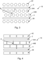
- Figure 4 shows an RF component 10 according to an embodiment of this disclosure.
- the RF component comprises a first electrically conductive signal member 2 for conveying an RF signal and a second electrically conductive signal member 4 for conveying an RF signal.
- the first and second electrically conductive signal members 2, 4 are transmission lines e.g. strip lines.
- the electrically conductive signal members 2, 4 could be other kinds of components, such as antennae.
- the first and second electrically conductive signal members 2, 4 may be provided in a laminated structure such as a metallization stack including a plurality of dielectric layers and layers of patterned metal features.
- the metallization stack may be located on a substrate such as a printed circuit board (PCB) or on a semiconductor substrate such as on the surface of a semiconductor die.
- PCB printed circuit board
- Electrically conductive side walls 42, 46 may be provided at either lateral side of the RF component 10. Similarly, upper and lower electrically conductive walls may be provided above and below the first and second electrically conductive signal members 2, 4, as described above in relation to Figure 1 . Each electrically conductive signal member 2, 4 may be located within a respective dielectric region as described above in relation to Figure 1 . The dielectric regions may be enclosed by the electrically conductive side walls 42, 46 and the upper and lower electrically conductive walls.
- the electrically conductive features, including the electrically conductive signal members 2, 4, the electrically conductive side walls 42, 46, the upper and lower electrically conductive walls (and the barrier to be described below) may be formed as the patterned metal features of a metallisation stack.
- the side walls 42, 46, the first electrically conductive signal member 2, the second electrically conductive signal member 4 and the barrier (to be described below) in this embodiment may be elongate and may coextend along a longitudinal axis of the RF component 10.
- the first electrically conductive signal member 2 and the second electrically conductive signal member 4 in this embodiment form strip lines.
- the elongate, coextensive arrangement shown in Figure 4 is not essential, particularly, for example, where the electrically conductive signal members 2, 4 form RF components other than strip lines (e.g. antennae).
- the embodiment shown in Figure 4 is provided with a barrier.
- the barrier is electrically conductive (e.g. metallic) and is located between the first electrically conductive signal member 2 and the second electrically conductive signal member 4, and between the upper and lower electrically conductive walls (where such walls are included).
- the barrier in this embodiment is formed by a plurality of electrically conductive shielding members 44A, 44B.
- Each electrically conductive shielding member comprises a polyhedron formed from an electrically conductive material (e.g. metal).
- the sidewalls 12, 16 in this embodiment may also be provided as polyhedra formed from an electrically conductive material (e.g. metal), although this is not essential (e.g. vias of the kind shown in Figure 3 could be used).
- the barrier comprises a first row of electrically conductive shielding members 44A spaced apart along a longitudinal axis of the first row, and a second row of electrically conductive shielding members 44B spaced apart along a longitudinal axis of the second row.
- the electrically conductive shielding members 44A of the first row are offset (staggered) with respect to the electrically conductive shielding members 44B of the second row. This can prevent a direct line of sight between the first electrically conductive signal member 2 and the second electrically conductive signal member 4, thereby improving the electromagnetic shielding providing by the barrier.
- any electromagnetic radiation passing through the barrier must navigate a plurality of turns or corners in order to reach the other one of the electrically conductive signal members.
- the offset is chosen such that a gap located between each electrically conductive shielding member 44A of the first row is located opposite a middle of an electrically conductive shielding member 44B of the second row, although this is not essential and other offsets could also be used.
- polyhedra for the electrically conductive shielding members of the barrier has a number of advantages.
- the use of polyhedra is readily compatible with standard semiconductor manufacturing techniques, such as the formation of metallization stacks. Because of this, a high degree of flexibility is achieved in terms of choosing the shape and size of the electrically conductive shielding members, whereby the shielding provided by the barrier can be optimised.
- Each electrically conductive shielding member in each row may be elongate (e.g. as shown in Figure 4 ).
- a longitudinal axis of each electrically conductive shielding member may extend substantially parallel to a longitudinal axis of the barrier itself.
- a longitudinal axis of each polyhedron in each row may be substantially parallel to a longitudinal axis of that row.
- the longitudinal axis of the first row may be 44A substantially parallel to the longitudinal axis of the second row 44B.
- each electrically conductive shielding member in each row 44A, 44B may be the same shape and size. It will be appreciated that at the ends of the barrier, one or more of the electrically conductive shielding members may need to be a different shape, owing to the offset nature of the arrangement of the electrically conductive shielding members in the barrier.
- each electrically conductive shielding member 44A, 44B comprises a polyhedron, which can simplify the manufacturing process as polyhedra in general are compatible with known metallization techniques in the semiconductor industry.
- a polyhedron may be considered to be a three-dimensional shape with flat polygonal faces, straight edges and sharp corners or vertices. Note that the vias 24A, 24B do not fall within this definition.
- each polyhedron comprises a rectangular cuboid.
- the rectangular cuboid may be elongate.
- the rectangular cuboid may be a square cuboid.
- the use of a rectangular cuboid provides a simple shape for layout purposes and manufacture, while still allowing the prevention of any direct line of sight between the electrically conductive signal members 2, 4.
- Figure 5 shows an RF component 10 including two strip lines 2, 4, according to another embodiment of this disclosure.
- the RF component 10 again comprises a first electrically conductive signal member 2 for conveying an RF signal and a second electrically conductive signal member 4 for conveying an RF signal.
- the first and second electrically conductive signal members 2, 4 are transmission lines e.g. strip lines.
- the electrically conductive signal members 2, 4 could be other kinds of components, such as antennae.
- the first and second electrically conductive signal members 2, 4 in this embodiment may be provided in a laminated structure such as a metallization stack including a plurality of dielectric layers and layers of patterned metal features.
- the metallization stack may be located on a substrate such as a printed circuit board (PCB) or on a semiconductor substrate such as on the surface of a semiconductor die.
- PCB printed circuit board
- electrically conductive side walls 52, 56 may be provided at either lateral side of the RF component 10.
- upper and lower electrically conductive walls may be provided above and below the first and second electrically conductive signal members 2, 4, as described above in relation to Figure 1 .
- each electrically conductive signal member 2, 4 may be located within a respective dielectric region as described above in relation to Figure 1 .
- the dielectric regions may be enclosed by the electrically conductive side walls 42, 46 and the upper and lower electrically conductive walls.
- the electrically conductive features including the electrically conductive signal members 2, 4, the electrically conductive side walls 42, 46, the upper and lower electrically conductive walls (and the barrier to be described below) may be formed as the patterned metal features of a metallisation stack, as described above.
- the side walls 52, 56, the first electrically conductive signal member 2, the second electrically conductive signal member 4 and the barrier (to be described below) in this embodiment may be elongate and may coextend along a longitudinal axis of the RF component 10.
- the first electrically conductive signal member 2 and the second electrically conductive signal member 4 in this embodiment form strip lines.
- the elongate, coextensive arrangement shown in Figure 5 is not essential, particularly, for example, where the electrically conductive signal members 2, 4 form RF components other than strip lines (e.g. antennae).
- the barrier in this embodiment comprises a first row of electrically conductive shielding members 54A spaced apart along a longitudinal axis of the first row and a second row of electrically conductive shielding members 54B spaced apart along a longitudinal axis of the second row.
- Each electrically conductive shielding member 54A, 54B comprises a polyhedron.
- the polyhedra used for the electrically conductive shielding members 54A, 54B in this embodiment collectively form a labyrinthine structure which, as can be seen from the arrow labelled C in Figure 5 , prevents a direct line of sight between the electrically conductive signal members 2, 4.
- the labyrinthine structure can increase the path length for electromagnetic fields attempting to pass through the barrier and by requiring the fields to navigate multiple (e.g. at least three, four, five or even more) turns within the barrier (again, see the arrow labelled C in Figure 5 ). This arrangement can increase the isolation between the electrically conductive signal members 2, 4.
- each electrically conductive shielding member 54A of the first row comprises a base portion having a first end and a second end, a first arm extending from the first end of the base towards the second row, and a second arm extending from the second end of the base towards the second row.
- each electrically conductive shielding member of the second row comprises a base portion having a first end and a second end, a first arm extending from the first end of the base towards the first row, and a second arm extending from the second end of the base towards the first row.
- the polyhedra of the electrically conductive shielding members 54A, 54B are thus substantially "U" shaped.
- the arms of the U-shaped electrically conductive shielding members 54A, 54B are interlocked, that is to say that a distal end of each arm of each electrically conductive shielding member 54A of the first row is located within a region located between the arms of an electrically conductive shielding member 54B of the second row (and vice versa).
- This interlocking of the arms of the electrically conductive shielding members 54A, 54B can, as demonstrated by the arrow labelled C in Figure 5 , increase the number of turns that electromagnetic fields attempting to pass through the barrier must navigate.
- the barrier includes two rows of electrically conductive shielding members 54A, 54B.
- the barrier may have more than two (three, four, five, etc.) rows of electrically conductive shielding members 54A, 54B.
- the electrically conductive shielding members 54A, 54B of the additional rows may also comprise a polyhedra.
- any additional rows of electrically conductive shielding members 54A, 54B in the barrier can further improve the isolation between the electrically conductive signal members 2, 4.
- the additional rows may be used to increase the path length for any electromagnetic fields attempting to pass through the barrier by introducing yet further turns that the electromagnetic fields must navigate.
- FIG. 6 shows a semiconductor device 100 according to a further embodiment of this disclosure.
- the device 100 in this embodiment comprises a package 110.
- the package contains an RF component 10 of the kind described herein.
- FIG. 7 shows a method 200 of making a Radio Frequency, "RF", component 10 of the kind described herein, according to another embodiment of this disclosure.
- a first electrically conductive signal member 2 for conveying an RF signal is formed.
- the first electrically conductive signal member 2 may be of the kind described above in relation to Figures 4 to 6 .
- a second electrically conductive signal member 4 for conveying an RF signal is formed.
- the second electrically conductive signal member 4 may be of the kind described above in relation to Figures 4 to 6 .
- a barrier located between the first electrically conductive signal member and the second electrically conductive signal member is formed.
- the barrier is for electromagnetically shielding the first and second electrically conductive signal members from each other.
- the barrier may be of the kind described above in relation to Figures 4 to 6 .
- the steps 202, 204, 206 may include deposit and patterning a plurality of layers of electrically conductive material and deposit and patterning a plurality layers of dielectric on a surface. As described herein, the layers may build up to form a metallization stack.
- the surface upon which the stack is formed may, for example, be the surface of a substrate such as a printed circuit board (PCB) or the surface of a semiconductor substrate such as a semiconductor die.
- PCB printed circuit board
- Figure 7 presents the formation of the electrically conductive signal members 2, 4 and the barrier in separate steps in which the electrically conductive signal members 2, 4 are formed first, it will be appreciated that these features could be formed in a different order (e.g. the barrier could be formed before the electrically conductive signal members 2, 4). It is also envisaged that these features could be formed simultaneously, that is to say in the same step.
- the component comprises a first electrically conductive signal member for conveying an RF signal and a second electrically conductive signal member for conveying an RF signal.
- the component also comprises a barrier located between the first signal member and the second signal member electromagnetically to shield the first and second signal members from each other.
- the barrier comprises a first row of electrically conductive shielding members spaced apart along a longitudinal axis of the first row, and a second row of electrically conductive shielding members spaced apart along a longitudinal axis of the second row.
- Each shielding member comprises a polyhedron.
- the shielding members of the first row are offset with respect to the shielding members of the second row to prevent a direct line of sight between the first signal member and the second signal member.
Landscapes
- Engineering & Computer Science (AREA)
- Microelectronics & Electronic Packaging (AREA)
- Physics & Mathematics (AREA)
- Electromagnetism (AREA)
- Optics & Photonics (AREA)
- Shielding Devices Or Components To Electric Or Magnetic Fields (AREA)
- Noise Elimination (AREA)
Abstract
Description
- The present specification relates to a Radio Frequency (RF) component and a method of making an RF component.
- In many RF components, it is necessary to provide electromagnetic shielding between two elements, such as transmission lines or antennae, so as to mitigate against electromagnetic interference between the two components.
- Aspects of the present disclosure are set out in the accompanying independent and dependent claims. Combinations of features from the dependent claims may be combined with features of the independent claims as appropriate and not merely as explicitly set out in the claims.
- According to an aspect of the present disclosure, there is provided a Radio Frequency, "RF", component comprising:
- a first electrically conductive signal member for conveying an RF signal;
- a second electrically conductive signal member for conveying an RF signal; and
- a barrier located between the first electrically conductive signal member and the second electrically conductive signal member electromagnetically to shield the first and second electrically conductive signal members from each other, wherein the barrier comprises:
- a first row of electrically conductive shielding members spaced apart along a longitudinal axis of the first row, wherein each electrically conductive shielding member in the first row comprises a polyhedron; and
- a second row of electrically conductive shielding members spaced apart along a longitudinal axis of the second row, wherein each electrically conductive shielding member in the second row comprises a polyhedron; and
- According to another aspect of the present disclosure, there is provided a method of making a Radio Frequency, "RF", component, the method comprising forming:
- a first electrically conductive signal member for conveying an RF signal;
- a second electrically conductive signal member for conveying an RF signal; and
- a barrier located between the first electrically conductive signal member and the second electrically conductive signal member electromagnetically to shield the first and second electrically conductive signal members from each other, wherein the barrier comprises:
- a first row of electrically conductive shielding members spaced apart along a longitudinal axis of the first row, wherein each electrically conductive shielding member in the first row comprises a polyhedron; and
- a second row of electrically conductive shielding members spaced apart along a longitudinal axis of the second row, wherein each electrically conductive shielding member in the second row comprises a polyhedron; and
- The provision of a barrier comprising rows of electrically conductive shielding members comprising polyhedra can provide greater design flexibility in customising the shape and configuration of the barrier for electromagnetically shielding the first and second electrically conductive signal members from each other. The use of polyhedra can also improve the electromagnetic isolation provided between the first and second electrically conductive signal members, particularly in combination with the offset provided between the first and second rows of electrically conductive shielding members.
- Each electrically conductive shielding member in each row may be elongate. This can further improve the isolation provided between the first and second electrically conductive signal members. For instance, the long dimension of each electrically conductive shielding member may be made greater than the gaps located between each electrically conductive shielding member in each row.
- A longitudinal axis of each polyhedron in each row may be substantially parallel to the longitudinal axis of that row. This can maximise the laterally facing profile of each electrically conductive shielding member in each row, again improving the isolation provided between the first and second electrically conductive signal members.
- The longitudinal axis of the first row may be substantially parallel to the longitudinal axis of the second row.
- Each electrically conductive shielding member in each row may be the same shape and size. This can make the shielding provided by the barrier more uniform along the length of the rows.
- The electrically conductive shielding members of the first row may be offset with respect to the electrically conductive shielding members of the second row such that a gap located between each electrically conductive shielding member of the first row is located opposite a middle of an electrically conductive shielding member of the second row. This can improve the isolation provided between the first and second electrically conductive signal members by increasing the path length for electromagnetic fields attempting to pass through the barrier.
- Each electrically conductive shielding member in each row may be a rectangular cuboid. This can simplify the manufacturing process.
- The electrically conductive shielding members of the rows of the barrier may collectively form a labyrinthine structure. This can improve the isolation provided between the first and second electrically conductive signal members by increasing the path length for electromagnetic fields attempting to pass through the barrier and by requiring the fields to navigate multiple (e.g. at least three, four, five or even more) turns within the barrier.
- Each electrically conductive shielding member of the first row may comprise:
- a base portion having a first end and a second end;
- a first arm extending from the first end of the base towards the second row; and
- a second arm extending from the second end of the base towards the second row.
- Each electrically conductive shielding member of the second row may comprise:
- a base portion having a first end and a second end;
- a first arm extending from the first end of the base towards the first row; and
- a second arm extending from the second end of the base towards the first row.
- A distal end of each arm of each electrically conductive shielding member of the first row may be located within a region located between the arms of an electrically conductive shielding member of the second row. This can force electromagnetic fields attempting to pass through the barrier to navigate additional turns within the barrier.
- A distal end of each arm of each electrically conductive shielding member of the second row may be located within a region located between the arms of an electrically conductive shielding member of the first row. This can force electromagnetic fields attempting to pass through the barrier to navigate additional turns within the barrier.
- The barrier may comprise at least one further row of electrically conductive shielding members spaced apart along a longitudinal axis of that further row. Each electrically conductive shielding member in the or each further row may comprise a polyhedron.
- The first electrically conductive signal member may comprise a transmission line.
- The second electrically conductive signal member may comprise a transmission line.
- The first electrically conductive signal member may comprise an antenna.
- The second electrically conductive signal member may comprise an antenna.
- According to a further aspect of the present disclosure, there is provided a semiconductor device comprising a package containing an RF component of the kind set out above.
- For the purposes of the present disclosure, "Radio Frequency" (RF) refers to a frequency in the range 300 GHz ≥ f ≥ 20 kHz.
- Embodiments of this disclosure will be described hereinafter, by way of example only, with reference to the accompanying drawings in which like reference signs relate to like elements and in which:
-
Figure 1 shows an example of an RF component including two strip lines; -
Figure 2 shows another view of the RF component ofFigure 1 ; -
Figure 3 shows another example of an RF component including two strip lines; -
Figure 4 shows an RF component including two strip lines, according to an embodiment of this disclosure; -
Figure 5 shows an RF component including two strip lines, according to another embodiment of this disclosure; -
Figure 6 shows a semiconductor device according to a further embodiment of this disclosure; and -
Figure 7 shows a method of making a Radio Frequency, "RF", component according to another embodiment of this disclosure. - Embodiments of this disclosure are described in the following with reference to the accompanying drawings.
-
Figures 1 and 2 show an example of anRF component 10 including a first electricallyconductive signal member 2 for conveying an RF signal and a second electricallyconductive signal member 4 for conveying an RF signal.Figure 1 is a cross section of theRF component 10 through the longitudinal axes of the electricallyconductive signal members 2, 4 (e.g. along the line A-A inFigure 2) and Figure 2 is a plan view of theRF component 10. - In this example, the first and second electrically
conductive signal members conductive signal members - The first and second electrically
conductive signal members conductive side walls RF component 10. Similarly, upper and lower electricallyconductive walls 18 may be provided above and below the first and second electricallyconductive signal members conductive signal member dielectric region dielectric regions conductive side walls conductive walls 18. The electrically conductive features, including the electricallyconductive signal members conductive side walls barrier 14 to be described below) may be formed as the patterned metal features of the metallisation stack. - In order to provide electromagnetic shielding of the first electrically
conductive signal member 2 from the second electrically conductive signal member 4 (and vice versa), the example shown inFigures 1 and 2 is provided with abarrier 14. Thebarrier 14 is electrically conductive (e.g. metallic) and is located between the first electricallyconductive signal member 2 and the second electricallyconductive signal member 4, and between the upper and lower electricallyconductive walls 18. - As can be seen from
Figure 2 , in this example, theside walls conductive signal member 2, the second electricallyconductive signal member 4 and thebarrier 14 are elongate and coextend along a longitudinal axis of theRF component 10. As noted above, the first electricallyconductive signal member 2 and the second electricallyconductive signal member 4 in this example form strip lines. It will be appreciated that the elongate, coextensive arrangement shown inFigure 2 is not essential, particularly, for example, where the electricallyconductive signal members - The
barrier 14 in this example is formed by a monolithic metallic block. Similarly, thesidewalls barrier 14 comprising a monolithic block may be seen as the ideal case for the purposes of providing electromagnetic shielding between the first electricallyconductive signal member 2 and the second electricallyconductive signal member 4. However, the provision of amonolithic barrier 14 andside walls Figures 1 and 2 is generally not possible, due to manufacturing constraints. For example, it is generally not possible to enclose the electricallyconductive signal members -
Figure 3 shows another example of anRF component 10 including twostrip lines Figure 3 uses linear rows of electrically conductive vias instead of monolithic blocks for the side walls and barrier described above in relation toFigures 1 and 2 . In particular, a row of electricallyconductive vias 22 forms theside wall 12, a row of electricallyconductive vias 26 forms theside wall 16, and one or more rows of electrically conductive vias 24A, 24B form thebarrier 14. Thevias Figure 3 may also comprise upper and lower electricallyconductive walls 18 of the kind shown inFigure 1 . - Although more feasible from a manufacturing perspective, the barrier in the example of
Figure 3 provides a lower degree of electromagnetic shielding than themonolithic barrier 14 shown inFigures 1 and 2 . In particular, it will be appreciated that electromagnetic fields may extend through the gaps between the vias. To mitigate against this, where multiple rows of electrically conductive vias 24A, 24B are provided, thevias 24A may be offset (staggered) with respect to the vias 24B in another row (this is illustrated inFigure 3 ), which may prevent there being a direct line of sight between the first electricallyconductive signal member 2 and the second electricallyconductive signal member 4 in a direction orthogonal to the longitudinal axes of the electricallyconductive signal members - Although the example in
Figure 3 is practical to manufacture, certain constraints remain. For example, the size of the via wall may be restricted due to warpage, de-gas during curing and other production technology reasons. -
Figure 4 shows anRF component 10 according to an embodiment of this disclosure. In this embodiment, the RF component comprises a first electricallyconductive signal member 2 for conveying an RF signal and a second electricallyconductive signal member 4 for conveying an RF signal. In this embodiment, the first and second electricallyconductive signal members conductive signal members - The first and second electrically
conductive signal members - Electrically
conductive side walls RF component 10. Similarly, upper and lower electrically conductive walls may be provided above and below the first and second electricallyconductive signal members Figure 1 . Each electricallyconductive signal member Figure 1 . The dielectric regions may be enclosed by the electricallyconductive side walls conductive signal members conductive side walls - As can be seen from
Figure 4 , in this example, theside walls conductive signal member 2, the second electricallyconductive signal member 4 and the barrier (to be described below) in this embodiment may be elongate and may coextend along a longitudinal axis of theRF component 10. As noted above, the first electricallyconductive signal member 2 and the second electricallyconductive signal member 4 in this embodiment form strip lines. It will be appreciated that the elongate, coextensive arrangement shown inFigure 4 is not essential, particularly, for example, where the electricallyconductive signal members - In order to provide electromagnetic shielding of the first electrically
conductive signal member 2 from the second electrically conductive signal member 4 (and vice versa), the embodiment shown inFigure 4 is provided with a barrier. The barrier is electrically conductive (e.g. metallic) and is located between the first electricallyconductive signal member 2 and the second electricallyconductive signal member 4, and between the upper and lower electrically conductive walls (where such walls are included). - The barrier in this embodiment is formed by a plurality of electrically
conductive shielding members sidewalls Figure 3 could be used). - In this embodiment, the barrier comprises a first row of electrically
conductive shielding members 44A spaced apart along a longitudinal axis of the first row, and a second row of electricallyconductive shielding members 44B spaced apart along a longitudinal axis of the second row. In this embodiment, the electricallyconductive shielding members 44A of the first row are offset (staggered) with respect to the electricallyconductive shielding members 44B of the second row. This can prevent a direct line of sight between the first electricallyconductive signal member 2 and the second electricallyconductive signal member 4, thereby improving the electromagnetic shielding providing by the barrier. As shown by the arrow labelled "A" inFigure 4 , any electromagnetic radiation passing through the barrier must navigate a plurality of turns or corners in order to reach the other one of the electrically conductive signal members. In this embodiment, the offset is chosen such that a gap located between each electricallyconductive shielding member 44A of the first row is located opposite a middle of an electricallyconductive shielding member 44B of the second row, although this is not essential and other offsets could also be used. - The use of polyhedra for the electrically conductive shielding members of the barrier has a number of advantages. The use of polyhedra is readily compatible with standard semiconductor manufacturing techniques, such as the formation of metallization stacks. Because of this, a high degree of flexibility is achieved in terms of choosing the shape and size of the electrically conductive shielding members, whereby the shielding provided by the barrier can be optimised.
- Each electrically conductive shielding member in each row may be elongate (e.g. as shown in
Figure 4 ). A longitudinal axis of each electrically conductive shielding member may extend substantially parallel to a longitudinal axis of the barrier itself. Also, a longitudinal axis of each polyhedron in each row may be substantially parallel to a longitudinal axis of that row. The longitudinal axis of the first row may be 44A substantially parallel to the longitudinal axis of thesecond row 44B. - Note that the arrangement shown in
Figure 4 can prevent any direct line of sight between the electricallyconductive signal members 2, 4 (this may be contrasted with the arrow labelled "B" inFigure 3 ). - To simplify the manufacturing process, each electrically conductive shielding member in each
row - Various shapes for the electrically
conductive shielding members conductive shielding member vias - In the embodiment shown in
Figure 4 , each polyhedron comprises a rectangular cuboid. The rectangular cuboid may be elongate. For example, the rectangular cuboid may be a square cuboid. The use of a rectangular cuboid provides a simple shape for layout purposes and manufacture, while still allowing the prevention of any direct line of sight between the electricallyconductive signal members - As will be described below, more complicated types of polyhedra are envisaged, for enhancing the isolation between the electrically
conductive signal members -
Figure 5 shows anRF component 10 including twostrip lines RF component 10 again comprises a first electricallyconductive signal member 2 for conveying an RF signal and a second electricallyconductive signal member 4 for conveying an RF signal. In this embodiment, the first and second electricallyconductive signal members conductive signal members - As described above, the first and second electrically
conductive signal members - As described above, electrically
conductive side walls RF component 10. Similarly, upper and lower electrically conductive walls may be provided above and below the first and second electricallyconductive signal members Figure 1 . Again, each electricallyconductive signal member Figure 1 . The dielectric regions may be enclosed by the electricallyconductive side walls conductive signal members conductive side walls - As can be seen from
Figure 5 , in this example, theside walls conductive signal member 2, the second electricallyconductive signal member 4 and the barrier (to be described below) in this embodiment may be elongate and may coextend along a longitudinal axis of theRF component 10. As noted above, the first electricallyconductive signal member 2 and the second electricallyconductive signal member 4 in this embodiment form strip lines. It will be appreciated that the elongate, coextensive arrangement shown inFigure 5 is not essential, particularly, for example, where the electricallyconductive signal members - The barrier in this embodiment comprises a first row of electrically
conductive shielding members 54A spaced apart along a longitudinal axis of the first row and a second row of electricallyconductive shielding members 54B spaced apart along a longitudinal axis of the second row. Each electricallyconductive shielding member - The polyhedra used for the electrically
conductive shielding members Figure 5 , prevents a direct line of sight between the electricallyconductive signal members Figure 5 ). This arrangement can increase the isolation between the electricallyconductive signal members - Although various labyrinthine structures may be used, depending on the exact shape chosen for the electrically
conductive shielding members conductive shielding member 54A of the first row comprises a base portion having a first end and a second end, a first arm extending from the first end of the base towards the second row, and a second arm extending from the second end of the base towards the second row. Similarly, each electrically conductive shielding member of the second row comprises a base portion having a first end and a second end, a first arm extending from the first end of the base towards the first row, and a second arm extending from the second end of the base towards the first row. The polyhedra of the electricallyconductive shielding members - To complete the labyrinthine structure of the present embodiment, the arms of the U-shaped electrically
conductive shielding members conductive shielding member 54A of the first row is located within a region located between the arms of an electricallyconductive shielding member 54B of the second row (and vice versa). This interlocking of the arms of the electricallyconductive shielding members Figure 5 , increase the number of turns that electromagnetic fields attempting to pass through the barrier must navigate. - In the embodiments described above in relation to
Figures 4 and5 , the barrier includes two rows of electricallyconductive shielding members conductive shielding members conductive shielding members - The provision of any additional rows of electrically
conductive shielding members conductive signal members -
Figure 6 shows asemiconductor device 100 according to a further embodiment of this disclosure. Thedevice 100 in this embodiment comprises apackage 110. The package contains anRF component 10 of the kind described herein. -
Figure 7 shows amethod 200 of making a Radio Frequency, "RF",component 10 of the kind described herein, according to another embodiment of this disclosure. - In a
first step 202, a first electricallyconductive signal member 2 for conveying an RF signal is formed. The first electricallyconductive signal member 2 may be of the kind described above in relation toFigures 4 to 6 . - In a
second step 204, a second electricallyconductive signal member 4 for conveying an RF signal is formed. The second electricallyconductive signal member 4 may be of the kind described above in relation toFigures 4 to 6 . - In a
third step 206, a barrier located between the first electrically conductive signal member and the second electrically conductive signal member is formed. The barrier is for electromagnetically shielding the first and second electrically conductive signal members from each other. The barrier may be of the kind described above in relation toFigures 4 to 6 . - The
steps Figure 7 presents the formation of the electricallyconductive signal members conductive signal members conductive signal members 2, 4). It is also envisaged that these features could be formed simultaneously, that is to say in the same step. - Accordingly, there has been described a Radio Frequency, "RF", component and a method of making the same. The component comprises a first electrically conductive signal member for conveying an RF signal and a second electrically conductive signal member for conveying an RF signal. The component also comprises a barrier located between the first signal member and the second signal member electromagnetically to shield the first and second signal members from each other. The barrier comprises a first row of electrically conductive shielding members spaced apart along a longitudinal axis of the first row, and a second row of electrically conductive shielding members spaced apart along a longitudinal axis of the second row. Each shielding member comprises a polyhedron. The shielding members of the first row are offset with respect to the shielding members of the second row to prevent a direct line of sight between the first signal member and the second signal member.
- Although particular embodiments of this disclosure have been described, it will be appreciated that many modifications/additions and/or substitutions may be made within the scope of the claims.
Claims (15)
- A Radio Frequency, "RF", component comprising:a first electrically conductive signal member for conveying an RF signal;a second electrically conductive signal member for conveying an RF signal; anda barrier located between the first electrically conductive signal member and the second electrically conductive signal member electromagnetically to shield the first and second electrically conductive signal members from each other, wherein the barrier comprises:a first row of electrically conductive shielding members spaced apart along a longitudinal axis of the first row, wherein each electrically conductive shielding member in the first row comprises a polyhedron; anda second row of electrically conductive shielding members spaced apart along a longitudinal axis of the second row, wherein each electricallyconductive shielding member in the second row comprises a polyhedron; and wherein the electrically conductive shielding members of the first row are offset with respect to the electrically conductive shielding members of the second row to prevent a direct line of sight between the first electrically conductive signal member and the second electrically conductive signal member.
- The RF component of claim 1, wherein each electrically conductive shielding member in each row is elongate.
- The RF component of claim 2, wherein a longitudinal axis of each polyhedron in each row is substantially parallel to the longitudinal axis of that row.
- The RF component of claim 3, wherein the longitudinal axis of the first row is substantially parallel to the longitudinal axis of the second row.
- The RF component of any preceding claim, wherein each electrically conductive shielding member in each row is the same shape and size.
- The RF component of any preceding claim, wherein the electrically conductive shielding members of the first row are offset with respect to the electrically conductive shielding members of the second row such that a gap located between each electrically conductive shielding member of the first row is located opposite a middle of an electrically conductive shielding member of the second row.
- The RF component of any preceding claim, wherein each electrically conductive shielding member in each row comprises a rectangular cuboid.
- The RF component of any of claims 1 to 6, wherein the electrically conductive shielding members of the rows of the barrier collectively form a labyrinthine structure.
- The RF component of claim 8, wherein:each electrically conductive shielding member of the first row comprises:a base portion having a first end and a second end;a first arm extending from the first end of the base towards the second row; anda second arm extending from the second end of the base towards the second row;each electrically conductive shielding member of the second row comprises:a base portion having a first end and a second end;a first arm extending from the first end of the base towards the first row; anda second arm extending from the second end of the base towards the first row.
- The RF component of claim 9, wherein a distal end of each arm of each electrically conductive shielding member of the first row is located within a region located between the arms of an electrically conductive shielding member of the second row.
- The RF component of any preceding claim, wherein the barrier comprises at least one further row of electrically conductive shielding members spaced apart along a longitudinal axis of that further row, wherein each electrically conductive shielding member in the or each further row comprises a polyhedron.
- The RF component of any preceding claim, wherein the first electrically conductive signal member and/or the second electrically conductive signal member comprise a transmission line.
- The RF component of any or claims 1 to 11, wherein the first electrically conductive signal member and/or the second electrically conductive signal member comprise an antenna.
- A semiconductor device comprising a package containing an RF component according to any preceding claim.
- A method of making a Radio Frequency, "RF", component, the method comprising forming:a first electrically conductive signal member for conveying an RF signal;a second electrically conductive signal member for conveying an RF signal; anda barrier located between the first electrically conductive signal member and the second electrically conductive signal member electromagnetically to shield the first and second electrically conductive signal members from each other, wherein the barrier comprises:a first row of electrically conductive shielding members spaced apart along a longitudinal axis of the first row, wherein each electrically conductive shielding member in the first row comprises a polyhedron; anda second row of electrically conductive shielding members spaced apart along a longitudinal axis of the second row, wherein each electricallyconductive shielding member in the second row comprises a polyhedron; and wherein the electrically conductive shielding members of the first row are offset with respect to the electrically conductive shielding members of the second row to prevent a direct line of sight between the first electrically conductive signal member and the second electrically conductive signal member.
Priority Applications (3)
| Application Number | Priority Date | Filing Date | Title |
|---|---|---|---|
| EP21213985.1A EP4195402B1 (en) | 2021-12-13 | 2021-12-13 | Rf component and method |
| CN202211394877.4A CN116264762A (en) | 2021-12-13 | 2022-11-08 | RF components and methods |
| US18/059,611 US12114472B2 (en) | 2021-12-13 | 2022-11-29 | RF component and method |
Applications Claiming Priority (1)
| Application Number | Priority Date | Filing Date | Title |
|---|---|---|---|
| EP21213985.1A EP4195402B1 (en) | 2021-12-13 | 2021-12-13 | Rf component and method |
Publications (2)
| Publication Number | Publication Date |
|---|---|
| EP4195402A1 true EP4195402A1 (en) | 2023-06-14 |
| EP4195402B1 EP4195402B1 (en) | 2025-10-15 |
Family
ID=78844708
Family Applications (1)
| Application Number | Title | Priority Date | Filing Date |
|---|---|---|---|
| EP21213985.1A Active EP4195402B1 (en) | 2021-12-13 | 2021-12-13 | Rf component and method |
Country Status (3)
| Country | Link |
|---|---|
| US (1) | US12114472B2 (en) |
| EP (1) | EP4195402B1 (en) |
| CN (1) | CN116264762A (en) |
Citations (4)
| Publication number | Priority date | Publication date | Assignee | Title |
|---|---|---|---|---|
| US10608345B2 (en) * | 2017-04-13 | 2020-03-31 | Nidec Corporation | Slot array antenna |
| US20200176884A1 (en) * | 2016-04-05 | 2020-06-04 | Nidec Corporation | Waveguide device and antenna array |
| US20200185802A1 (en) * | 2018-12-06 | 2020-06-11 | Samsung Electronics Co., Ltd. | Ridge gap waveguide and multilayer antenna array including the same |
| CN113013642A (en) * | 2021-02-25 | 2021-06-22 | 北京邮电大学 | Array antenna and communication equipment |
Family Cites Families (17)
| Publication number | Priority date | Publication date | Assignee | Title |
|---|---|---|---|---|
| US4658334A (en) * | 1986-03-19 | 1987-04-14 | Rca Corporation | RF signal shielding enclosure of electronic systems |
| US5150088A (en) | 1991-03-27 | 1992-09-22 | Hughes Aircraft Company | Stripline shielding techniques in low temperature co-fired ceramic |
| US5384555A (en) | 1993-01-26 | 1995-01-24 | Harris Corporation | Combined RF and digital/DC signalling interconnect laminate |
| US6157546A (en) * | 1999-03-26 | 2000-12-05 | Ericsson Inc. | Shielding apparatus for electronic devices |
| US6974724B2 (en) | 2004-04-28 | 2005-12-13 | Nokia Corporation | Shielded laminated structure with embedded chips |
| US7330156B2 (en) | 2004-08-20 | 2008-02-12 | Nokia Corporation | Antenna isolation using grounded microwave elements |
| KR100699472B1 (en) | 2005-09-27 | 2007-03-26 | 삼성전자주식회사 | Flat Panel Array Antenna with Isolation Element |
| US7637776B2 (en) * | 2006-05-17 | 2009-12-29 | Leviton Manufacturing Co., Inc. | Communication cabling with shielding separator system and method |
| TWI360918B (en) | 2007-10-04 | 2012-03-21 | Realtek Semiconductor Corp | Multiple antenna system |
| US8854266B2 (en) | 2011-08-23 | 2014-10-07 | Apple Inc. | Antenna isolation elements |
| WO2014099389A1 (en) * | 2012-12-20 | 2014-06-26 | 3M Innovative Properties Company | Floating connector shield |
| US9419667B2 (en) | 2013-04-16 | 2016-08-16 | Skyworks Solutions, Inc. | Apparatus and methods related to conformal coating implemented with surface mount devices |
| US10464306B2 (en) * | 2015-04-17 | 2019-11-05 | Board Of Regents, The University Of Texas System | Metal objects spanning internal cavities in structures fabricated by additive manufacturing |
| US10206317B2 (en) * | 2015-06-29 | 2019-02-12 | Microsoft Technology Licensing, Llc | Modular radio frequency shielding |
| US9899341B2 (en) | 2016-07-18 | 2018-02-20 | Atmel Corporation | Antenna on integrated circuit package |
| US10177095B2 (en) * | 2017-03-24 | 2019-01-08 | Amkor Technology, Inc. | Semiconductor device and method of manufacturing thereof |
| US10714430B2 (en) | 2017-07-21 | 2020-07-14 | Octavo Systems Llc | EMI shield for molded packages |
-
2021
- 2021-12-13 EP EP21213985.1A patent/EP4195402B1/en active Active
-
2022
- 2022-11-08 CN CN202211394877.4A patent/CN116264762A/en active Pending
- 2022-11-29 US US18/059,611 patent/US12114472B2/en active Active
Patent Citations (4)
| Publication number | Priority date | Publication date | Assignee | Title |
|---|---|---|---|---|
| US20200176884A1 (en) * | 2016-04-05 | 2020-06-04 | Nidec Corporation | Waveguide device and antenna array |
| US10608345B2 (en) * | 2017-04-13 | 2020-03-31 | Nidec Corporation | Slot array antenna |
| US20200185802A1 (en) * | 2018-12-06 | 2020-06-11 | Samsung Electronics Co., Ltd. | Ridge gap waveguide and multilayer antenna array including the same |
| CN113013642A (en) * | 2021-02-25 | 2021-06-22 | 北京邮电大学 | Array antenna and communication equipment |
Also Published As
| Publication number | Publication date |
|---|---|
| US20230189492A1 (en) | 2023-06-15 |
| EP4195402B1 (en) | 2025-10-15 |
| US12114472B2 (en) | 2024-10-08 |
| CN116264762A (en) | 2023-06-16 |
Similar Documents
| Publication | Publication Date | Title |
|---|---|---|
| EP3780259B1 (en) | Transition structure and multilayer transition structure for millimeter wave | |
| KR101067118B1 (en) | Dielectric resonator antenna embedded in multilayer board | |
| KR101119354B1 (en) | Dielectric resonant antenna embedded in multilayer substrate for enhancing bandwidth | |
| US11387016B2 (en) | Transmission line substrate and electronic device | |
| US9698487B2 (en) | Array antenna | |
| US9184505B2 (en) | Dielectric cavity antenna | |
| US9893433B2 (en) | Array antenna | |
| CN104054215B (en) | Dual polarized antenna for sending and receiving separation | |
| EP1775795A1 (en) | Broadband proximity-coupled cavity backed patch antenna | |
| EP0978896B1 (en) | Transmission line and transmission line resonator | |
| US20170244174A1 (en) | Antenna apparatus and surface current suppression filter for antenna apparatus | |
| US8378893B2 (en) | Patch antenna | |
| US11631940B2 (en) | Waveguide slot antenna | |
| WO2020057756A1 (en) | Surface wave reduction for antenna structures | |
| US9226388B2 (en) | Printed circuit board | |
| US12469986B2 (en) | Antenna device and antenna module | |
| JP6418352B2 (en) | Antenna device | |
| US12114472B2 (en) | RF component and method | |
| KR100914440B1 (en) | Printed circuit board with a stepped conductive layer | |
| US11342676B2 (en) | Antenna | |
| EP2107638A1 (en) | Half-mode substrate integrated antenna structure | |
| KR20250068614A (en) | Patch antenna array with improved radiation efficiency | |
| US10511076B2 (en) | RF coupler including vertically stacked coupling sections having conductive layers disposed between the coupling sections and the coupler including a surrounding electric shield | |
| US10950946B2 (en) | Antenna, module substrate, and module | |
| KR102940456B1 (en) | Three dimensional true time delay system |
Legal Events
| Date | Code | Title | Description |
|---|---|---|---|
| PUAI | Public reference made under article 153(3) epc to a published international application that has entered the european phase |
Free format text: ORIGINAL CODE: 0009012 |
|
| STAA | Information on the status of an ep patent application or granted ep patent |
Free format text: STATUS: THE APPLICATION HAS BEEN PUBLISHED |
|
| AK | Designated contracting states |
Kind code of ref document: A1 Designated state(s): AL AT BE BG CH CY CZ DE DK EE ES FI FR GB GR HR HU IE IS IT LI LT LU LV MC MK MT NL NO PL PT RO RS SE SI SK SM TR |
|
| STAA | Information on the status of an ep patent application or granted ep patent |
Free format text: STATUS: REQUEST FOR EXAMINATION WAS MADE |
|
| 17P | Request for examination filed |
Effective date: 20231214 |
|
| RBV | Designated contracting states (corrected) |
Designated state(s): AL AT BE BG CH CY CZ DE DK EE ES FI FR GB GR HR HU IE IS IT LI LT LU LV MC MK MT NL NO PL PT RO RS SE SI SK SM TR |
|
| GRAP | Despatch of communication of intention to grant a patent |
Free format text: ORIGINAL CODE: EPIDOSNIGR1 |
|
| STAA | Information on the status of an ep patent application or granted ep patent |
Free format text: STATUS: GRANT OF PATENT IS INTENDED |
|
| INTG | Intention to grant announced |
Effective date: 20250516 |
|
| GRAS | Grant fee paid |
Free format text: ORIGINAL CODE: EPIDOSNIGR3 |
|
| GRAA | (expected) grant |
Free format text: ORIGINAL CODE: 0009210 |
|
| STAA | Information on the status of an ep patent application or granted ep patent |
Free format text: STATUS: THE PATENT HAS BEEN GRANTED |
|
| AK | Designated contracting states |
Kind code of ref document: B1 Designated state(s): AL AT BE BG CH CY CZ DE DK EE ES FI FR GB GR HR HU IE IS IT LI LT LU LV MC MK MT NL NO PL PT RO RS SE SI SK SM TR |
|
| REG | Reference to a national code |
Ref country code: GB Ref legal event code: FG4D Ref country code: CH Ref legal event code: F10 Free format text: ST27 STATUS EVENT CODE: U-0-0-F10-F00 (AS PROVIDED BY THE NATIONAL OFFICE) Effective date: 20251015 |
|
| REG | Reference to a national code |
Ref country code: DE Ref legal event code: R096 Ref document number: 602021040358 Country of ref document: DE |
|
| REG | Reference to a national code |
Ref country code: IE Ref legal event code: FG4D |
|
| PGFP | Annual fee paid to national office [announced via postgrant information from national office to epo] |
Ref country code: DE Payment date: 20251126 Year of fee payment: 5 |
|
| PGFP | Annual fee paid to national office [announced via postgrant information from national office to epo] |
Ref country code: AT Payment date: 20260113 Year of fee payment: 5 |
|
| PGFP | Annual fee paid to national office [announced via postgrant information from national office to epo] |
Ref country code: FR Payment date: 20251120 Year of fee payment: 5 |
|
| REG | Reference to a national code |
Ref country code: NL Ref legal event code: MP Effective date: 20251015 |
|
| REG | Reference to a national code |
Ref country code: AT Ref legal event code: MK05 Ref document number: 1847871 Country of ref document: AT Kind code of ref document: T Effective date: 20251015 |
|
| PG25 | Lapsed in a contracting state [announced via postgrant information from national office to epo] |
Ref country code: NL Free format text: LAPSE BECAUSE OF FAILURE TO SUBMIT A TRANSLATION OF THE DESCRIPTION OR TO PAY THE FEE WITHIN THE PRESCRIBED TIME-LIMIT Effective date: 20251015 |
|
| PG25 | Lapsed in a contracting state [announced via postgrant information from national office to epo] |
Ref country code: ES Free format text: LAPSE BECAUSE OF FAILURE TO SUBMIT A TRANSLATION OF THE DESCRIPTION OR TO PAY THE FEE WITHIN THE PRESCRIBED TIME-LIMIT Effective date: 20251015 |
|
| REG | Reference to a national code |
Ref country code: LT Ref legal event code: MG9D |
|
| PG25 | Lapsed in a contracting state [announced via postgrant information from national office to epo] |
Ref country code: NO Free format text: LAPSE BECAUSE OF FAILURE TO SUBMIT A TRANSLATION OF THE DESCRIPTION OR TO PAY THE FEE WITHIN THE PRESCRIBED TIME-LIMIT Effective date: 20260115 |
|
| PG25 | Lapsed in a contracting state [announced via postgrant information from national office to epo] |
Ref country code: AT Free format text: LAPSE BECAUSE OF FAILURE TO SUBMIT A TRANSLATION OF THE DESCRIPTION OR TO PAY THE FEE WITHIN THE PRESCRIBED TIME-LIMIT Effective date: 20251015 Ref country code: HR Free format text: LAPSE BECAUSE OF FAILURE TO SUBMIT A TRANSLATION OF THE DESCRIPTION OR TO PAY THE FEE WITHIN THE PRESCRIBED TIME-LIMIT Effective date: 20251015 Ref country code: FI Free format text: LAPSE BECAUSE OF FAILURE TO SUBMIT A TRANSLATION OF THE DESCRIPTION OR TO PAY THE FEE WITHIN THE PRESCRIBED TIME-LIMIT Effective date: 20251015 |
|
| PG25 | Lapsed in a contracting state [announced via postgrant information from national office to epo] |
Ref country code: RS Free format text: LAPSE BECAUSE OF FAILURE TO SUBMIT A TRANSLATION OF THE DESCRIPTION OR TO PAY THE FEE WITHIN THE PRESCRIBED TIME-LIMIT Effective date: 20260115 |
|
| PG25 | Lapsed in a contracting state [announced via postgrant information from national office to epo] |
Ref country code: IS Free format text: LAPSE BECAUSE OF FAILURE TO SUBMIT A TRANSLATION OF THE DESCRIPTION OR TO PAY THE FEE WITHIN THE PRESCRIBED TIME-LIMIT Effective date: 20260215 |
|
| PG25 | Lapsed in a contracting state [announced via postgrant information from national office to epo] |
Ref country code: PT Free format text: LAPSE BECAUSE OF FAILURE TO SUBMIT A TRANSLATION OF THE DESCRIPTION OR TO PAY THE FEE WITHIN THE PRESCRIBED TIME-LIMIT Effective date: 20260216 |
|
| PG25 | Lapsed in a contracting state [announced via postgrant information from national office to epo] |
Ref country code: PL Free format text: LAPSE BECAUSE OF FAILURE TO SUBMIT A TRANSLATION OF THE DESCRIPTION OR TO PAY THE FEE WITHIN THE PRESCRIBED TIME-LIMIT Effective date: 20251015 |
|
| PG25 | Lapsed in a contracting state [announced via postgrant information from national office to epo] |
Ref country code: LV Free format text: LAPSE BECAUSE OF FAILURE TO SUBMIT A TRANSLATION OF THE DESCRIPTION OR TO PAY THE FEE WITHIN THE PRESCRIBED TIME-LIMIT Effective date: 20251015 |
|
| PG25 | Lapsed in a contracting state [announced via postgrant information from national office to epo] |
Ref country code: BG Free format text: LAPSE BECAUSE OF FAILURE TO SUBMIT A TRANSLATION OF THE DESCRIPTION OR TO PAY THE FEE WITHIN THE PRESCRIBED TIME-LIMIT Effective date: 20251015 |
|
| PG25 | Lapsed in a contracting state [announced via postgrant information from national office to epo] |
Ref country code: RO Free format text: LAPSE BECAUSE OF FAILURE TO SUBMIT A TRANSLATION OF THE DESCRIPTION OR TO PAY THE FEE WITHIN THE PRESCRIBED TIME-LIMIT Effective date: 20251015 |
|
| PG25 | Lapsed in a contracting state [announced via postgrant information from national office to epo] |
Ref country code: LT Free format text: LAPSE BECAUSE OF FAILURE TO SUBMIT A TRANSLATION OF THE DESCRIPTION OR TO PAY THE FEE WITHIN THE PRESCRIBED TIME-LIMIT Effective date: 20251015 |
|
| PG25 | Lapsed in a contracting state [announced via postgrant information from national office to epo] |
Ref country code: SM Free format text: LAPSE BECAUSE OF FAILURE TO SUBMIT A TRANSLATION OF THE DESCRIPTION OR TO PAY THE FEE WITHIN THE PRESCRIBED TIME-LIMIT Effective date: 20251015 |
|
| PG25 | Lapsed in a contracting state [announced via postgrant information from national office to epo] |
Ref country code: MC Free format text: LAPSE BECAUSE OF FAILURE TO SUBMIT A TRANSLATION OF THE DESCRIPTION OR TO PAY THE FEE WITHIN THE PRESCRIBED TIME-LIMIT Effective date: 20251015 |
|
| PG25 | Lapsed in a contracting state [announced via postgrant information from national office to epo] |
Ref country code: DK Free format text: LAPSE BECAUSE OF FAILURE TO SUBMIT A TRANSLATION OF THE DESCRIPTION OR TO PAY THE FEE WITHIN THE PRESCRIBED TIME-LIMIT Effective date: 20251015 |
|
| PG25 | Lapsed in a contracting state [announced via postgrant information from national office to epo] |
Ref country code: IT Free format text: LAPSE BECAUSE OF FAILURE TO SUBMIT A TRANSLATION OF THE DESCRIPTION OR TO PAY THE FEE WITHIN THE PRESCRIBED TIME-LIMIT Effective date: 20251015 |
|
| PG25 | Lapsed in a contracting state [announced via postgrant information from national office to epo] |
Ref country code: EE Free format text: LAPSE BECAUSE OF FAILURE TO SUBMIT A TRANSLATION OF THE DESCRIPTION OR TO PAY THE FEE WITHIN THE PRESCRIBED TIME-LIMIT Effective date: 20251015 |
|
| PG25 | Lapsed in a contracting state [announced via postgrant information from national office to epo] |
Ref country code: CZ Free format text: LAPSE BECAUSE OF FAILURE TO SUBMIT A TRANSLATION OF THE DESCRIPTION OR TO PAY THE FEE WITHIN THE PRESCRIBED TIME-LIMIT Effective date: 20251015 |
|
| REG | Reference to a national code |
Ref country code: CH Ref legal event code: H13 Free format text: ST27 STATUS EVENT CODE: U-0-0-H10-H13 (AS PROVIDED BY THE NATIONAL OFFICE) Effective date: 20260723 |
|
| PG25 | Lapsed in a contracting state [announced via postgrant information from national office to epo] |
Ref country code: SK Free format text: LAPSE BECAUSE OF FAILURE TO SUBMIT A TRANSLATION OF THE DESCRIPTION OR TO PAY THE FEE WITHIN THE PRESCRIBED TIME-LIMIT Effective date: 20251015 |
|
| PG25 | Lapsed in a contracting state [announced via postgrant information from national office to epo] |
Ref country code: SE Free format text: LAPSE BECAUSE OF FAILURE TO SUBMIT A TRANSLATION OF THE DESCRIPTION OR TO PAY THE FEE WITHIN THE PRESCRIBED TIME-LIMIT Effective date: 20251015 |