EP4195274A1 - Method for forming semiconductor structure and semiconductor structure - Google Patents
Method for forming semiconductor structure and semiconductor structure Download PDFInfo
- Publication number
- EP4195274A1 EP4195274A1 EP21859772.2A EP21859772A EP4195274A1 EP 4195274 A1 EP4195274 A1 EP 4195274A1 EP 21859772 A EP21859772 A EP 21859772A EP 4195274 A1 EP4195274 A1 EP 4195274A1
- Authority
- EP
- European Patent Office
- Prior art keywords
- support
- layer
- forming
- sub
- interconnect
- Prior art date
- Legal status (The legal status is an assumption and is not a legal conclusion. Google has not performed a legal analysis and makes no representation as to the accuracy of the status listed.)
- Pending
Links
Images



Classifications
-
- H—ELECTRICITY
- H10—SEMICONDUCTOR DEVICES; ELECTRIC SOLID-STATE DEVICES NOT OTHERWISE PROVIDED FOR
- H10B—ELECTRONIC MEMORY DEVICES
- H10B12/00—Dynamic random access memory [DRAM] devices
- H10B12/01—Manufacture or treatment
- H10B12/02—Manufacture or treatment for one transistor one-capacitor [1T-1C] memory cells
-
- H—ELECTRICITY
- H10—SEMICONDUCTOR DEVICES; ELECTRIC SOLID-STATE DEVICES NOT OTHERWISE PROVIDED FOR
- H10B—ELECTRONIC MEMORY DEVICES
- H10B12/00—Dynamic random access memory [DRAM] devices
- H10B12/01—Manufacture or treatment
- H10B12/09—Manufacture or treatment with simultaneous manufacture of the peripheral circuit region and memory cells
-
- H—ELECTRICITY
- H10—SEMICONDUCTOR DEVICES; ELECTRIC SOLID-STATE DEVICES NOT OTHERWISE PROVIDED FOR
- H10B—ELECTRONIC MEMORY DEVICES
- H10B12/00—Dynamic random access memory [DRAM] devices
- H10B12/30—DRAM devices comprising one-transistor - one-capacitor [1T-1C] memory cells
-
- H—ELECTRICITY
- H10—SEMICONDUCTOR DEVICES; ELECTRIC SOLID-STATE DEVICES NOT OTHERWISE PROVIDED FOR
- H10P—GENERIC PROCESSES OR APPARATUS FOR THE MANUFACTURE OR TREATMENT OF DEVICES COVERED BY CLASS H10
- H10P50/00—Etching of wafers, substrates or parts of devices
- H10P50/73—Etching of wafers, substrates or parts of devices using masks for insulating materials
-
- H—ELECTRICITY
- H10—SEMICONDUCTOR DEVICES; ELECTRIC SOLID-STATE DEVICES NOT OTHERWISE PROVIDED FOR
- H10W—GENERIC PACKAGES, INTERCONNECTIONS, CONNECTORS OR OTHER CONSTRUCTIONAL DETAILS OF DEVICES COVERED BY CLASS H10
- H10W20/00—Interconnections in chips, wafers or substrates
- H10W20/01—Manufacture or treatment
- H10W20/031—Manufacture or treatment of conductive parts of the interconnections
- H10W20/056—Manufacture or treatment of conductive parts of the interconnections by filling conductive material into holes, grooves or trenches
-
- H—ELECTRICITY
- H10—SEMICONDUCTOR DEVICES; ELECTRIC SOLID-STATE DEVICES NOT OTHERWISE PROVIDED FOR
- H10W—GENERIC PACKAGES, INTERCONNECTIONS, CONNECTORS OR OTHER CONSTRUCTIONAL DETAILS OF DEVICES COVERED BY CLASS H10
- H10W20/00—Interconnections in chips, wafers or substrates
- H10W20/01—Manufacture or treatment
- H10W20/071—Manufacture or treatment of dielectric parts thereof
- H10W20/081—Manufacture or treatment of dielectric parts thereof by forming openings in the dielectric parts
- H10W20/089—Manufacture or treatment of dielectric parts thereof by forming openings in the dielectric parts using processes for implementing desired shapes or dispositions of the openings, e.g. double patterning
-
- H—ELECTRICITY
- H10—SEMICONDUCTOR DEVICES; ELECTRIC SOLID-STATE DEVICES NOT OTHERWISE PROVIDED FOR
- H10W—GENERIC PACKAGES, INTERCONNECTIONS, CONNECTORS OR OTHER CONSTRUCTIONAL DETAILS OF DEVICES COVERED BY CLASS H10
- H10W20/00—Interconnections in chips, wafers or substrates
- H10W20/40—Interconnections external to wafers or substrates, e.g. back-end-of-line [BEOL] metallisations or vias connecting to gate electrodes
- H10W20/41—Interconnections external to wafers or substrates, e.g. back-end-of-line [BEOL] metallisations or vias connecting to gate electrodes characterised by their conductive parts
- H10W20/435—Cross-sectional shapes or dispositions of interconnections
-
- H—ELECTRICITY
- H10—SEMICONDUCTOR DEVICES; ELECTRIC SOLID-STATE DEVICES NOT OTHERWISE PROVIDED FOR
- H10B—ELECTRONIC MEMORY DEVICES
- H10B10/00—Static random access memory [SRAM] devices
- H10B10/18—Peripheral circuit regions
-
- H—ELECTRICITY
- H10—SEMICONDUCTOR DEVICES; ELECTRIC SOLID-STATE DEVICES NOT OTHERWISE PROVIDED FOR
- H10B—ELECTRONIC MEMORY DEVICES
- H10B12/00—Dynamic random access memory [DRAM] devices
- H10B12/01—Manufacture or treatment
- H10B12/02—Manufacture or treatment for one transistor one-capacitor [1T-1C] memory cells
- H10B12/03—Making the capacitor or connections thereto
- H10B12/033—Making the capacitor or connections thereto the capacitor extending over the transistor
- H10B12/0335—Making a connection between the transistor and the capacitor, e.g. plug
-
- H—ELECTRICITY
- H10—SEMICONDUCTOR DEVICES; ELECTRIC SOLID-STATE DEVICES NOT OTHERWISE PROVIDED FOR
- H10B—ELECTRONIC MEMORY DEVICES
- H10B12/00—Dynamic random access memory [DRAM] devices
- H10B12/50—Peripheral circuit region structures
-
- H—ELECTRICITY
- H10—SEMICONDUCTOR DEVICES; ELECTRIC SOLID-STATE DEVICES NOT OTHERWISE PROVIDED FOR
- H10B—ELECTRONIC MEMORY DEVICES
- H10B20/00—Read-only memory [ROM] devices
- H10B20/60—Peripheral circuit regions
-
- H—ELECTRICITY
- H10—SEMICONDUCTOR DEVICES; ELECTRIC SOLID-STATE DEVICES NOT OTHERWISE PROVIDED FOR
- H10B—ELECTRONIC MEMORY DEVICES
- H10B41/00—Electrically erasable-and-programmable ROM [EEPROM] devices comprising floating gates
- H10B41/40—Electrically erasable-and-programmable ROM [EEPROM] devices comprising floating gates characterised by the peripheral circuit region
-
- H—ELECTRICITY
- H10—SEMICONDUCTOR DEVICES; ELECTRIC SOLID-STATE DEVICES NOT OTHERWISE PROVIDED FOR
- H10B—ELECTRONIC MEMORY DEVICES
- H10B43/00—EEPROM devices comprising charge-trapping gate insulators
- H10B43/40—EEPROM devices comprising charge-trapping gate insulators characterised by the peripheral circuit region
-
- H—ELECTRICITY
- H10—SEMICONDUCTOR DEVICES; ELECTRIC SOLID-STATE DEVICES NOT OTHERWISE PROVIDED FOR
- H10B—ELECTRONIC MEMORY DEVICES
- H10B51/00—Ferroelectric RAM [FeRAM] devices comprising ferroelectric memory transistors
- H10B51/40—Ferroelectric RAM [FeRAM] devices comprising ferroelectric memory transistors characterised by the peripheral circuit region
-
- H—ELECTRICITY
- H10—SEMICONDUCTOR DEVICES; ELECTRIC SOLID-STATE DEVICES NOT OTHERWISE PROVIDED FOR
- H10B—ELECTRONIC MEMORY DEVICES
- H10B53/00—Ferroelectric RAM [FeRAM] devices comprising ferroelectric memory capacitors
- H10B53/40—Ferroelectric RAM [FeRAM] devices comprising ferroelectric memory capacitors characterised by the peripheral circuit region
Definitions
- the present application relates to the field of semiconductors, and particularly to a method for forming a semiconductor structure and a semiconductor structure.
- a memory is one of the key devices that determine system performance.
- the memory is like a temporary warehouse, and is responsible for data transfer and temporary storage.
- the memory typically adopts a way that a transistor is connected to a memory capacitor to constitute a memory cell, and controls a process of charging/discharging the memory capacitor through the conduction of the transistor.
- a contact structure is typically used to resolve the difference between the arrangement of the transistors and the arrangement of the memory capacitors.
- the coverage area of the contact structure may be too large, the stress on the contact structure is too large, causing metal peeling of the memory, which affects the yield of the formed memory.
- the embodiments of the present application provide a method for forming a semiconductor structure and a semiconductor structure, which resolve the difference between the arrangement of the transistors and the arrangement of the memory capacitors by forming a contact structure with a smaller coverage area, and avoid metal peeling of the memory.
- the embodiments of the present application provide a method for forming a semiconductor structure, which includes the following operations.
- a semiconductor substrate is provided, the semiconductor substrate including an array region and a peripheral region, a plurality of conductive layers being arranged in the array region and separated from each other.
- a support layer covering the semiconductor layer is formed, an interconnect layer being arranged in the support layer located on the array region, the interconnect layer extending to the peripheral region, the interconnect layer being electrically connected to a respective one of the conductive layers and transmitting an electrical signal of the respective one of the conductive layers to the peripheral region.
- the support layer is patterned to form a plurality of support structures located on the peripheral region and separated from each other and an interconnect structure located on the array region and the peripheral region, the interconnect layer being located in the interconnect structure, voids being provided between the support structures separated from each other to reduce an area of the peripheral region occupied by the support structures.
- the support structures in the peripheral region and the interconnect structure in the array region that are simultaneously formed through a one etching process in this present application simplify the process flow, thereby reducing the manufacturing cost of the semiconductor structure. Furthermore, the support structures located on the peripheral region and separated from each other and the presence of voids, which are formed through patterning, greatly reduce the area of the peripheral region occupied by the support structures, thereby reducing the stress on the support structures and preventing metal peeling from occurring in the memory formed by the above-mentioned semiconductor structure.
- the operation that the support layer covering the semiconductor substrate is formed may include the following operation. N sub-support layers stacked one after another are sequentially formed to constitute the support layer, where N is a natural number greater than or equal to 2.
- an i th sub-support layer may include the following operations.
- An i th sub-support film is formed at a top surface of a (i-1) th sub-support layer, and an i th sub-interconnect layer is formed in the i th sub-support film to constitute the i th sub-support layer, where i is a natural number greater than or equal to 2 and less than or equal to N.
- the operation that the i th sub-interconnect layer is formed in the i th sub-support film may include the following operations. A part of the i th sub-support film is etched to form an i th trench, a part of the formed sub-support layer is etched based on the i th trench until a part of the respective one of the conductive layers is exposed, to form an i th through hole, and the i th sub-interconnect layer filling the i th trench and the i th through hole is formed.
- the operation that the support layer covering the semiconductor substrate is formed may include the following operation.
- a support film covering the semiconductor substrate is formed, the support film is patterned to form through holes exposing the conductive layers, a remaining part of the support film constituting the support layer.
- the interconnect layer fills the through holes and is in contact with the conductive layers.
- the operation that the support structure is patterned may include the following operations.
- a mask layer and a patterned photoresist are sequentially formed on the support layer, the patterned photoresist including a first pattern located in the array region and a second pattern located in the peripheral region, the mask layer is patterned based on the patterned photoresist, and the support layer is patterned based on the mask layer.
- each of the formed support structures may be an I-shaped structure.
- the area of the peripheral region occupied by the support structures is greatly reduced and the I-shaped structure is stable.
- each of the formed support structures may have an I-shape with a length ranging from 0.2 um to 0.4 um and a width less than 0.15 um, and a gap of the I-shape may have a width ranging from 0.3 um to 0.5 um.
- each of the formed support structures may have an I-shape with a length of 0.3 um and a width of 0.05 um, and a gap of the I-shape may have a width of 0.4 um.
- the width of the I-shape of each of the formed support structures may be greater than twice a minimum line width of the semiconductor substrate.
- the embodiments of the present application further provide a semiconductor structure, including: a semiconductor substrate including an array region and a peripheral region, a plurality of conductive layers being arranged in the array region and separated from each other; a plurality of support structures separated from each other and located on the peripheral region, the support structures including a support layer, voids being provided between the support structures separated from each other to reduce an area of the peripheral region occupied by the support structures; and an interconnect structure located on the array region and the peripheral region, the interconnect structure including the support layer and an interconnect layer located in the support layer, the interconnect layer being electrically connected to a respective one of the conductive layers and transmitting an electrical signal of the respective one of the conductive layers to the peripheral region.
- the support layer may be a stack.
- each of the support structures may be an I-shaped structure.
- each of the support structures may have an I-shape with a length ranging from 0.2 um to 0.4 um and a width less than 0.15 um, and a gap of the I-shape may have a width ranging from 0.3 um to 0.5 um.
- each of the formed support structures may have an I-shape with a length of 0.3 um and a width of 0.05 um, and a gap of the I-shape may have a width of 0.4 um.
- the width of the I-shape of each of the support structures may be greater than twice a minimum line width of the semiconductor substrate.
- this present application reduces the area of the peripheral region occupied by the support structures, thereby reducing the stress on the support structures and preventing metal peeling from occurring in the memory formed by the above-mentioned semiconductor structure.
- FIG. 1 to FIG. 20 illustrate schematic diagrams of a semiconductor structure corresponding to operations provided in the embodiments of this present application.
- a contact structure is typically used to resolve the difference between the arrangement of the transistors and the arrangement of the memory capacitors.
- the coverage area of the contact structure may be too large, the stress on the contact structure is too large, causing metal peeling of the memory, which affects the yield of the formed memory.
- an embodiment of the present application provides a method for forming a semiconductor structure, which includes the following operations.
- a semiconductor substrate is provided.
- the semiconductor substrate includes an array region and a peripheral region, and a plurality of conductive layers are arranged in the array region and separated from each other.
- a support layer covering the semiconductor layer is formed.
- An interconnect layer is arranged in the support layer located on the array region and extends to the peripheral region.
- the interconnect layer is electrically connected to a respective one of the conductive layers and transmits an electrical signal of the respective one of the conductive layers to the peripheral region.
- the support layer is patterned to form a plurality of support structures located on the peripheral region and separated from each other and an interconnect structure located on the array region and the peripheral region.
- the interconnect layer is located in the interconnect structure. Voids are provided between the support structures separated from each other to reduce an area of the peripheral region occupied by the support structures.
- FIG. 1 to FIG. 20 illustrate schematic diagrams corresponding to operations of a method for forming a semiconductor structure provided by the embodiments of the present application.
- the method for forming the semiconductor structure provided in the embodiments will be described below in detail in combination with the drawing.
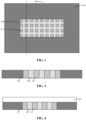
- FIG. 1 is a schematic diagram of a top view of a semiconductor substrate
- FIG. 2 is a schematic sectional view along a dashed line shown in Figure 1 .
- a semiconductor substrate 100 is provided.
- the semiconductor substrate 100 includes an array region 120 and a peripheral region 110.
- a plurality of conductive layer 121 are arranged in the array region 120 and separated from each other.
- the semiconductor substrate 100 provided in the embodiment is formed bit line structures and capacitive contact structures between the bit line structures.
- a top surface of the capacitive contact structure is exposed at a surface of the semiconductor substrate 100 to subsequently form a contact structure, to be electrically connected to a subsequently formed lower electrode plate of a memory capacitor.
- the exposed capacitive contact structure is the plurality of conductive layers 121 separated from each other mentioned above.
- a support layer 200 covering the semiconductor substrate 100 is formed.
- An interconnect layer is arranged in the support layer located on the array region 120 and extends to the peripheral region 110.
- the interconnect layer is electrically connected to a respective one of the conductive layers and transmits an electrical signal of the respective one of the conductive layers to the peripheral region 110.
- the support layer 200 is a stack that is sequentially formed.
- the operation that the support layer 200 covering the semiconductor substrate 100 is formed includes the following operation. N sub-support layers stacked one after another are sequentially formed to constitute the support layer 200, where N is a natural number greater than or equal to 2.
- N is equal to 4
- N may be a natural number greater than or equal to 2, such as 2, 3, or 5 etc.
- an i th sub-support layer includes the following operations.
- An i th sub-support film is formed at a top surface of a (i-1) th sub-support layer.
- An i th sub-interconnect layer is formed in the i th sub-support film to constitute the i th sub-support layer, where i is a natural number greater than or equal to 2 and less than or equal to N.
- a first sub-support film is formed at the top surface of the semiconductor substrate, and a first interconnect layer is formed in the first sub-support film to constitute a first sub-support layer.
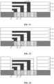
- a first sub-support film 201 covering the semiconductor substrate 100 is formed.
- the first sub-support film 201 is made of an insulating material, such as silicon nitride, silicon oxide, or silicon oxynitride.
- the material of the first sub-support film 201 is silicon nitride.
- a part of the first sub-support film 201 is etched to form a first trench that exposes the leftmost conductive layer 121 as shown in FIG. 4 .
- a left side of the sectional view corresponds to a lower side of the top view.
- the remaining part of the first sub-support film 201 constitutes a first sub-support layer 211.
- a first sub-interconnect layer 221 filling the first trench is formed.
- the first sub-interconnect layer 221 may be made of one or more conductive materials, such as doped poly-crystalline silicon, titanium, titanium nitride, tungsten, a composite of tungsten, or the like. In this embodiment, the material of the first sub-interconnect layer 221 is tungsten.
- a second sub-support film 202 covering the first sub-support film 211 is formed.
- the second sub-support film 202 is made of an insulating material, such as silicon nitride, silicon oxide, or silicon oxynitride.
- the material of the second sub-support film 202 is silicon nitride.
- a part of the second sub-support film 202 is etched to form a second trench, and the first sub-support layer 211 is etched based on the second trench until the second conductive layer 121 from the left shown in FIG. 7 is exposed.
- the remaining part of the second sub-support film 202 constitutes a second sub-support layer 212.
- a second sub-interconnect layer 222 filling the second trench and a second through hole is formed.
- the second sub-interconnect layer 222 may be made of one or more conductive materials, such as doped poly-crystalline silicon, titanium, titanium nitride, tungsten, a composite of tungsten, or the like. In this embodiment, the material of the second sub-interconnect layer 222 is tungsten.
- a third sub-support film 203 covering the second sub-support layer 212 is formed.
- the third sub-support film 203 is made of an insulating material, such as silicon nitride, silicon oxide, or silicon oxynitride.
- the material of the third sub-support film 203 is silicon nitride.
- a part of the third sub-support film 203 is etched to form a third trench, and the second sub-support layer 212 and the first sub-support layer 211 are etched based on the third trench until the second conductive layer 121 from the right shown in FIG. 10 is exposed.
- a right side of the sectional view corresponds to an upper side of the top view, and the remaining part of the third sub-support film 203 constitutes a third sub-support layer 213.
- a third sub-interconnect layer 223 filling the third trench and a third through hole is formed.
- the third sub-interconnect layer 223 may be made of one or more conductive materials, such as doped poly-crystalline silicon, titanium, titanium nitride, tungsten, a composite of tungsten, or the like. In this embodiment, the material of the third sub-interconnect layer 223 is tungsten.
- a fourth sub-support film 204 covering the third sub-support film 213 is formed.
- the fourth sub-support film 204 is made of an insulating material, such as silicon nitride, silicon oxide, or silicon oxynitride.
- the material of the fourth sub-support film 204 is silicon nitride.
- a part of the fourth sub-support film 204 is etched to form a fourth trench, and the third sub-support layer 213, the second sub-support layer 212, and the first sub-support layer 211 are etched based on the fourth trench until the rightmost conductive layer 121 shown in FIG. 13 is exposed.
- a right side of the sectional view corresponds to an upper side of the top view, and the remaining part of the fourth sub-support film 204 constitutes a fourth sub-support layer 214.
- a fourth sub-interconnect layer 224 filling the fourth trench and a fourth through hole is formed.
- the fourth sub-interconnect layer 224 may be made of one or more conductive materials, such as doped poly-crystalline silicon, titanium, titanium nitride, tungsten, a composite of tungsten, or the like. In this embodiment, the material of the fourth sub-interconnect layer 224 is tungsten.
- the first sub-interconnect layer 221, the second sub-interconnect layer 222, the third sub-interconnect layer 223, and the fourth sub-interconnect layer 224 jointly constitute the interconnect layer.
- the first sub-support layer 211, the second sub-support layer 212, the third sub-support layer 213, and the fourth sub-support layer 214 jointly constitute the support layer 200.
- FIG. 15 is a schematic top view of an interconnect structure and an interconnect layer.
- the interconnect epitaxy is located in the peripheral region 110 to interconnect an electrical signal of the conductive layers 121 in the array region 120 with the peripheral region 110 for performance test on the conductive layers 121 subsequently connected to a test device. That is, a performance test on a formed capacity contact of a memory through the test device is subsequently formed.
- the interconnect epitaxy and the fourth sub-interconnect layer 224 are formed in one process so as to prevent the layers from being in contact with each other, and the conductive effect is good.
- the interconnect epitaxy and the fourth sub-interconnect layer may be deposited in different operations. Further, when the interconnect layer is formed by a stacked structure, the aspect ratio of a through hole that needs to be etched to form each sub-interconnect layer is small, so that the morphology of the through hole formed after etching is good, and the contact between the sub-interconnect layer and a respective one of the conductive layers 121 is good.
- the support layer and the interconnect layer may also be formed in a single-layer structure.
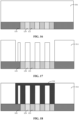
- a support film 301 covering the semiconductor substrate 100 is formed.
- the support film 301 is patterned to form through holes exposing the conductive layers 121.
- the remaining part of the support film 301 constitutes the support layer 311.
- An interconnect layer filling the through holes is formed.
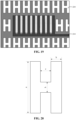
- the support layer 200 is patterned to form a plurality of support structures 220 located on the peripheral region 110 and separated from each other and an interconnect structure 210 located on the array region 120 and the peripheral region 110.
- the interconnect layer is located in the interconnect structure 220, and voids are provided between the support structures 210 separated from each other to reduce the area of the peripheral region 110 occupied by the support structures 210.
- the operation that the support layer 200 is patterned includes the following operations.
- a mask layer and a patterned photoresist are sequentially formed on the support layer 200.
- the patterned photoresist includes a first pattern located in the array region 120 and a second pattern located in the peripheral region 110.
- the mask layer is patterned based on the patterned photoresist, and the support layer is patterned based on the mask layer.
- the formed patterned photoresist includes a light-transmitting region and a light-blocking region.
- the light-blocking region constitutes the first pattern in the array region 120, and the first pattern is a top morphology of the interconnect structure.
- the light-blocking region constitutes the second pattern in the peripheral region 110, and the second pattern is a top morphology of the support structure, which may be round, square, I-shaped, or the like.
- the light transmittance of the light-transmitting region is greater than that of the light-blocking region. In the subsequent photolithography process, light can pass through the light-transmitting region to irradiate on the mask layer to etch the mask layer.
- the second pattern in the peripheral region 110 is I-shaped, that is, each of the formed support structures 220 is an I-shaped structure.
- the support structures can greatly reduce the area of the peripheral region 110 occupied by the support structures 220, thereby reducing the stress on the support structures 220 and thus preventing metal peeling from occurring in the formed semiconductor structure.
- the I-shaped structure has good stability and is not easy to collapse.
- each of the formed support structures has an I-shape with a length ranging from 0.2 um to 0.4 um, that is, the length indicated by a in the figure ranges from 0.2 um to 0.4 um, such as 0.25 um, 0.30 um, or 0.35 um.
- Each of the support structures has an I-shape with a width less than 0.15 um, that is, the width indicated by b in the figure is less than 0.15 um, such as 0.06 um, 0.09 um, or 0.12 um.
- a gap of each of the I-shaped support structures has a width ranging from 0.3 um to 0.5 um, that is, the width indicated by c in the figure ranges from 0.3 um to 0.5 um, such as 0.35 um, 0.40 um, or 0.45 um.
- a is equal to 0.30 um
- b is equal to 0.05 um
- c is equal to 0.40 um. Therefore, each of the I-shaped structures formed has larger space, which further reduces the coverage area of the contact structure.
- each of the formed I-shaped structure has an I-shape whose width is greater than twice the minimum line width of the semiconductor substrate 100. Therefore, the stability of the formed support structures 220 is further ensured.
- the support structures in the peripheral region and the interconnect structure in the array region are simultaneously formed through a one etching process in this present application, which simplifies the process flow, thereby reducing the manufacturing cost of the semiconductor structure. Furthermore, the support structures located on the peripheral region and separated from each other and voids, which are formed through patterning, greatly reduce the area of the peripheral region occupied by the support structures, thereby reducing the stress on the support structures and preventing metal peeling from occurring in the memory formed by the above-mentioned semiconductor structure.
- Another embodiment of the present application relates to a semiconductor structure.
- a semiconductor structure includes: a semiconductor substrate 100 including an array region 120 and a peripheral region110, a plurality of conductive layers 121 being arranged in the array region 120 and separated from each other; a plurality of support structures 220 separated from each other and located on the peripheral region 110, the support structures 220 including a support layer, voids being provided between the support structures 220 separated from each other to reduce the area of the peripheral region occupied by the support structure 220; an interconnect structure 210 located on the array region 120 and the peripheral region 110, the interconnect structure 210 including the support layer and an interconnect layer located in the support layer, the interconnect layer being electrically connected to a respective one of the conductive layers 121 and transmitting an electrical signal of the respective one of the conductive layers 121 to the peripheral region.
- the semiconductor substrate 100 provided in the embodiment is formed bit line structures and a capacitive contact structure between the bit line structures.
- a top surface of the capacitive contact structure is exposed to subsequently form a contact structure, to be electrically connected to a subsequently formed lower electrode plate of a memory capacity.
- the exposed capacitive contact structure is the above plurality of conductive layers 121 separated from each other.
- the interconnect structure 220 is a stack.
- the interconnect structure 220 formed by a 4-layer stack is taken as an example in this embodiment to specifically introduce the interconnect structure 220, and the number of layers of the stack does not constitute a limitation to the embodiments of the present application.
- the interconnect structure includes the first sub-interconnect layer, the second sub-interconnect layer, the third sub-interconnect layer, and the fourth sub-interconnect layer that are sequentially stacked on the semiconductor substrate.
- the first sub-interconnect layer, the second sub-interconnect layer, the third sub-interconnect layer, and the fourth sub-interconnect layer are configured to be connected to different conductive layers 121, transmit an electrical signal of the conductive layers 121 to the peripheral region 110, and are subsequently connected to the test device in the peripheral region 110 to test the performance of the conductive layers 121.
- each of the support structures 220 is an I-shaped structure.
- Each of the support structures 220 has an I-shape with a length ranging from 0.2 um to 0.4 um, such as 0.25 um, 0.30 um, or 0.35 um.
- Each of the support structures 220 has an I-shape with a width less than 0.15 um, such as 0.06 um, 0.09 um, or 0.12 um.
- a gap of the I-shaped support structure 220 has a width ranging from 0.3 um to 0.5 um, such as 0.35 um, 0.40 um, or 0.45 um.
- a is equal to 0.30 um
- b is equal to 0.05 um
- c is equal to 0.40 um. Therefore, each of the I-shaped structures formed has larger space, which further reduces the coverage area of the contact structure.
- the width of the I-shape of each of the formed I-shaped structures is greater than twice the minimum line width of the semiconductor substrate 100. Therefore, the stability of the formed support structure 220 is further ensured.
- this present application reduces the area of the peripheral region occupied by the support structures, thereby reducing the stress on the support structures and preventing metal peeling from occurring in the memory formed by the above-mentioned semiconductor structure.
Landscapes
- Engineering & Computer Science (AREA)
- Manufacturing & Machinery (AREA)
- Internal Circuitry In Semiconductor Integrated Circuit Devices (AREA)
Abstract
Description
- This application is based upon
Chinese Patent Application No. 202010880910.9, filed on August 27, 2020 - The present application relates to the field of semiconductors, and particularly to a method for forming a semiconductor structure and a semiconductor structure.
- A memory is one of the key devices that determine system performance. The memory is like a temporary warehouse, and is responsible for data transfer and temporary storage. The memory typically adopts a way that a transistor is connected to a memory capacitor to constitute a memory cell, and controls a process of charging/discharging the memory capacitor through the conduction of the transistor.
- In the manufacturing process of connecting the transistor and the memory capacitor, a contact structure is typically used to resolve the difference between the arrangement of the transistors and the arrangement of the memory capacitors. However, in the manufacturing process of the contact structure, since the coverage area of the contact structure may be too large, the stress on the contact structure is too large, causing metal peeling of the memory, which affects the yield of the formed memory.
- The embodiments of the present application provide a method for forming a semiconductor structure and a semiconductor structure, which resolve the difference between the arrangement of the transistors and the arrangement of the memory capacitors by forming a contact structure with a smaller coverage area, and avoid metal peeling of the memory.
- In order to solve the above-mentioned problem, the embodiments of the present application provide a method for forming a semiconductor structure, which includes the following operations. A semiconductor substrate is provided, the semiconductor substrate including an array region and a peripheral region, a plurality of conductive layers being arranged in the array region and separated from each other. A support layer covering the semiconductor layer is formed, an interconnect layer being arranged in the support layer located on the array region, the interconnect layer extending to the peripheral region, the interconnect layer being electrically connected to a respective one of the conductive layers and transmitting an electrical signal of the respective one of the conductive layers to the peripheral region. The support layer is patterned to form a plurality of support structures located on the peripheral region and separated from each other and an interconnect structure located on the array region and the peripheral region, the interconnect layer being located in the interconnect structure, voids being provided between the support structures separated from each other to reduce an area of the peripheral region occupied by the support structures.
- Compared with a method in a related art, the support structures in the peripheral region and the interconnect structure in the array region that are simultaneously formed through a one etching process in this present application simplify the process flow, thereby reducing the manufacturing cost of the semiconductor structure. Furthermore, the support structures located on the peripheral region and separated from each other and the presence of voids, which are formed through patterning, greatly reduce the area of the peripheral region occupied by the support structures, thereby reducing the stress on the support structures and preventing metal peeling from occurring in the memory formed by the above-mentioned semiconductor structure.
- Further, the operation that the support layer covering the semiconductor substrate is formed may include the following operation. N sub-support layers stacked one after another are sequentially formed to constitute the support layer, where N is a natural number greater than or equal to 2.
- Further, the operation that an ith sub-support layer is formed may include the following operations. An ith sub-support film is formed at a top surface of a (i-1)th sub-support layer, and an ith sub-interconnect layer is formed in the ith sub-support film to constitute the ith sub-support layer, where i is a natural number greater than or equal to 2 and less than or equal to N.
- Further, the operation that the ith sub-interconnect layer is formed in the ith sub-support film may include the following operations. A part of the ith sub-support film is etched to form an ith trench, a part of the formed sub-support layer is etched based on the ith trench until a part of the respective one of the conductive layers is exposed, to form an ith through hole, and the ith sub-interconnect layer filling the ith trench and the ith through hole is formed.
- Further, the operation that the support layer covering the semiconductor substrate is formed may include the following operation. A support film covering the semiconductor substrate is formed, the support film is patterned to form through holes exposing the conductive layers, a remaining part of the support film constituting the support layer. The interconnect layer fills the through holes and is in contact with the conductive layers.
- Further, the operation that the support structure is patterned may include the following operations. A mask layer and a patterned photoresist are sequentially formed on the support layer, the patterned photoresist including a first pattern located in the array region and a second pattern located in the peripheral region, the mask layer is patterned based on the patterned photoresist, and the support layer is patterned based on the mask layer.
- Further, each of the formed support structures may be an I-shaped structure. By forming the I-shaped support structure, the area of the peripheral region occupied by the support structures is greatly reduced and the I-shaped structure is stable.
- Further, each of the formed support structures may have an I-shape with a length ranging from 0.2 um to 0.4 um and a width less than 0.15 um, and a gap of the I-shape may have a width ranging from 0.3 um to 0.5 um.
- Further, each of the formed support structures may have an I-shape with a length of 0.3 um and a width of 0.05 um, and a gap of the I-shape may have a width of 0.4 um.
- Further, the width of the I-shape of each of the formed support structures may be greater than twice a minimum line width of the semiconductor substrate.
- The embodiments of the present application further provide a semiconductor structure, including: a semiconductor substrate including an array region and a peripheral region, a plurality of conductive layers being arranged in the array region and separated from each other; a plurality of support structures separated from each other and located on the peripheral region, the support structures including a support layer, voids being provided between the support structures separated from each other to reduce an area of the peripheral region occupied by the support structures; and an interconnect structure located on the array region and the peripheral region, the interconnect structure including the support layer and an interconnect layer located in the support layer, the interconnect layer being electrically connected to a respective one of the conductive layers and transmitting an electrical signal of the respective one of the conductive layers to the peripheral region.
- Further, the support layer may be a stack.
- Further, each of the support structures may be an I-shaped structure.
- Further, each of the support structures may have an I-shape with a length ranging from 0.2 um to 0.4 um and a width less than 0.15 um, and a gap of the I-shape may have a width ranging from 0.3 um to 0.5 um.
- Further, each of the formed support structures may have an I-shape with a length of 0.3 um and a width of 0.05 um, and a gap of the I-shape may have a width of 0.4 um.
- Further, the width of the I-shape of each of the support structures may be greater than twice a minimum line width of the semiconductor substrate.
- Compared with the method in the related art, this present application reduces the area of the peripheral region occupied by the support structures, thereby reducing the stress on the support structures and preventing metal peeling from occurring in the memory formed by the above-mentioned semiconductor structure.
-
FIG. 1 to FIG. 20 illustrate schematic diagrams of a semiconductor structure corresponding to operations provided in the embodiments of this present application. - At present, in the manufacturing process of connecting a transistor and a memory capacitor, a contact structure is typically used to resolve the difference between the arrangement of the transistors and the arrangement of the memory capacitors. However, in the manufacturing process of the contact structure, since the coverage area of the contact structure may be too large, the stress on the contact structure is too large, causing metal peeling of the memory, which affects the yield of the formed memory.
- In order to solve the above-mentioned problem, an embodiment of the present application provides a method for forming a semiconductor structure, which includes the following operations. A semiconductor substrate is provided. The semiconductor substrate includes an array region and a peripheral region, and a plurality of conductive layers are arranged in the array region and separated from each other. A support layer covering the semiconductor layer is formed. An interconnect layer is arranged in the support layer located on the array region and extends to the peripheral region. The interconnect layer is electrically connected to a respective one of the conductive layers and transmits an electrical signal of the respective one of the conductive layers to the peripheral region. The support layer is patterned to form a plurality of support structures located on the peripheral region and separated from each other and an interconnect structure located on the array region and the peripheral region. The interconnect layer is located in the interconnect structure. Voids are provided between the support structures separated from each other to reduce an area of the peripheral region occupied by the support structures.
- In order to make the objectives, technical solutions, and advantages of the embodiments of the present application clearer, each embodiment of the present application will be described below in detail in combination with the drawings. However, those of ordinary skill in the art can understand that, in each embodiment of the present application, many technical details are proposed to make readers understand the present application better. However, the technical solutions claimed by the present application may also be implemented even without these technical details and various variations and modifications made based on each of the following embodiments. Division of each of the following embodiments is for ease of description and should not form any limit to specific implementation modes of the present application. Each embodiment can be combined and refer to each other without conflicts.
-
FIG. 1 to FIG. 20 illustrate schematic diagrams corresponding to operations of a method for forming a semiconductor structure provided by the embodiments of the present application. The method for forming the semiconductor structure provided in the embodiments will be described below in detail in combination with the drawing. - Referring to
FIG. 1 and FIG. 2, FIG. 1 is a schematic diagram of a top view of a semiconductor substrate, andFIG. 2 is a schematic sectional view along a dashed line shown inFigure 1 . Asemiconductor substrate 100 is provided. Thesemiconductor substrate 100 includes anarray region 120 and aperipheral region 110. A plurality ofconductive layer 121 are arranged in thearray region 120 and separated from each other. - It is to be noted that the
semiconductor substrate 100 provided in the embodiment is formed bit line structures and capacitive contact structures between the bit line structures. A top surface of the capacitive contact structure is exposed at a surface of thesemiconductor substrate 100 to subsequently form a contact structure, to be electrically connected to a subsequently formed lower electrode plate of a memory capacitor. The exposed capacitive contact structure is the plurality ofconductive layers 121 separated from each other mentioned above. - Referring to
FIG. 3 to FIG. 15 , asupport layer 200 covering thesemiconductor substrate 100 is formed. An interconnect layer is arranged in the support layer located on thearray region 120 and extends to theperipheral region 110. The interconnect layer is electrically connected to a respective one of the conductive layers and transmits an electrical signal of the respective one of the conductive layers to theperipheral region 110. - In this embodiment, the
support layer 200 is a stack that is sequentially formed. The operation that thesupport layer 200 covering thesemiconductor substrate 100 is formed includes the following operation. N sub-support layers stacked one after another are sequentially formed to constitute thesupport layer 200, where N is a natural number greater than or equal to 2. - The operation that the
support layer 200 is formed in this embodiment will be described below in detail in combination with the drawing. It is to be noted that, in this embodiment, the formation of the stack where N is equal to 4 is taken as an example to describe and is not limitation to the embodiments of the present application. In other embodiments, N may be a natural number greater than or equal to 2, such as 2, 3, or 5 etc. - Specifically, the operation that an ith sub-support layer is formed includes the following operations. An ith sub-support film is formed at a top surface of a (i-1)th sub-support layer. An ith sub-interconnect layer is formed in the ith sub-support film to constitute the ith sub-support layer, where i is a natural number greater than or equal to 2 and less than or equal to N. In a case that i is equal to 1, a first sub-support film is formed at the top surface of the semiconductor substrate, and a first interconnect layer is formed in the first sub-support film to constitute a first sub-support layer.
- Referring to
FIG. 3 , a firstsub-support film 201 covering thesemiconductor substrate 100 is formed. - The first
sub-support film 201 is made of an insulating material, such as silicon nitride, silicon oxide, or silicon oxynitride. In this embodiment, the material of the firstsub-support film 201 is silicon nitride. - Referring to
FIG. 4 , a part of the firstsub-support film 201 is etched to form a first trench that exposes the leftmostconductive layer 121 as shown inFIG. 4 . A left side of the sectional view corresponds to a lower side of the top view. The remaining part of the firstsub-support film 201 constitutes a firstsub-support layer 211. - Referring to
FIG. 5 , a firstsub-interconnect layer 221 filling the first trench is formed. - The first
sub-interconnect layer 221 may be made of one or more conductive materials, such as doped poly-crystalline silicon, titanium, titanium nitride, tungsten, a composite of tungsten, or the like. In this embodiment, the material of the firstsub-interconnect layer 221 is tungsten. - Referring to
FIG. 6 , a secondsub-support film 202 covering the firstsub-support film 211 is formed. - The second
sub-support film 202 is made of an insulating material, such as silicon nitride, silicon oxide, or silicon oxynitride. In this embodiment, the material of the secondsub-support film 202 is silicon nitride. - Referring to
FIG. 7 , a part of the secondsub-support film 202 is etched to form a second trench, and the firstsub-support layer 211 is etched based on the second trench until the secondconductive layer 121 from the left shown inFIG. 7 is exposed. The remaining part of the secondsub-support film 202 constitutes a secondsub-support layer 212. - Referring to
FIG. 8 , a second sub-interconnect layer 222 filling the second trench and a second through hole is formed. - The second sub-interconnect layer 222 may be made of one or more conductive materials, such as doped poly-crystalline silicon, titanium, titanium nitride, tungsten, a composite of tungsten, or the like. In this embodiment, the material of the second sub-interconnect layer 222 is tungsten.
- Referring to
FIG. 9 , a thirdsub-support film 203 covering the secondsub-support layer 212 is formed. - The third
sub-support film 203 is made of an insulating material, such as silicon nitride, silicon oxide, or silicon oxynitride. In this embodiment, the material of the thirdsub-support film 203 is silicon nitride. - Referring to
FIG. 10 , a part of the thirdsub-support film 203 is etched to form a third trench, and the secondsub-support layer 212 and the firstsub-support layer 211 are etched based on the third trench until the secondconductive layer 121 from the right shown inFIG. 10 is exposed. A right side of the sectional view corresponds to an upper side of the top view, and the remaining part of the thirdsub-support film 203 constitutes a thirdsub-support layer 213. - Referring to
FIG. 11 , a thirdsub-interconnect layer 223 filling the third trench and a third through hole is formed. - The third
sub-interconnect layer 223 may be made of one or more conductive materials, such as doped poly-crystalline silicon, titanium, titanium nitride, tungsten, a composite of tungsten, or the like. In this embodiment, the material of the thirdsub-interconnect layer 223 is tungsten. - Referring to
FIG. 12 , a fourthsub-support film 204 covering the thirdsub-support film 213 is formed. - The fourth
sub-support film 204 is made of an insulating material, such as silicon nitride, silicon oxide, or silicon oxynitride. In this embodiment, the material of the fourthsub-support film 204 is silicon nitride. - Referring to
FIG. 13 , a part of the fourthsub-support film 204 is etched to form a fourth trench, and the thirdsub-support layer 213, the secondsub-support layer 212, and the firstsub-support layer 211 are etched based on the fourth trench until the rightmostconductive layer 121 shown inFIG. 13 is exposed. A right side of the sectional view corresponds to an upper side of the top view, and the remaining part of the fourthsub-support film 204 constitutes a fourthsub-support layer 214. - Referring to
FIG. 14 , a fourthsub-interconnect layer 224 filling the fourth trench and a fourth through hole is formed. - The fourth
sub-interconnect layer 224 may be made of one or more conductive materials, such as doped poly-crystalline silicon, titanium, titanium nitride, tungsten, a composite of tungsten, or the like. In this embodiment, the material of the fourthsub-interconnect layer 224 is tungsten. - The first
sub-interconnect layer 221, the second sub-interconnect layer 222, the thirdsub-interconnect layer 223, and the fourthsub-interconnect layer 224 jointly constitute the interconnect layer. The firstsub-support layer 211, the secondsub-support layer 212, the thirdsub-support layer 213, and the fourthsub-support layer 214 jointly constitute thesupport layer 200. - Referring to
FIG. 13 , during a formation of the fourth trench, an interconnect trench is formed in the peripheral region close to the leftmostconductive layer 121. Referring toFIG. 14 , when the fourthsub-interconnect layer 224 is formed, the interconnect trench is filled to form an interconnect epitaxy. Referring toFIG. 15, FIG. 15 is a schematic top view of an interconnect structure and an interconnect layer. The interconnect epitaxy is located in theperipheral region 110 to interconnect an electrical signal of theconductive layers 121 in thearray region 120 with theperipheral region 110 for performance test on theconductive layers 121 subsequently connected to a test device. That is, a performance test on a formed capacity contact of a memory through the test device is subsequently formed. - It is to be noted that, in this embodiment, the interconnect epitaxy and the fourth
sub-interconnect layer 224 are formed in one process so as to prevent the layers from being in contact with each other, and the conductive effect is good. - In other embodiments, the interconnect epitaxy and the fourth sub-interconnect layer may be deposited in different operations. Further, when the interconnect layer is formed by a stacked structure, the aspect ratio of a through hole that needs to be etched to form each sub-interconnect layer is small, so that the morphology of the through hole formed after etching is good, and the contact between the sub-interconnect layer and a respective one of the
conductive layers 121 is good. - In other embodiments, referring to
FIG. 16 to FIG. 18 , the support layer and the interconnect layer may also be formed in a single-layer structure. Specifically, referring toFIG. 16 , asupport film 301 covering thesemiconductor substrate 100 is formed. Thesupport film 301 is patterned to form through holes exposing theconductive layers 121. The remaining part of thesupport film 301 constitutes thesupport layer 311. An interconnect layer filling the through holes is formed. - Referring to
FIG. 19 , thesupport layer 200 is patterned to form a plurality ofsupport structures 220 located on theperipheral region 110 and separated from each other and aninterconnect structure 210 located on thearray region 120 and theperipheral region 110. The interconnect layer is located in theinterconnect structure 220, and voids are provided between thesupport structures 210 separated from each other to reduce the area of theperipheral region 110 occupied by thesupport structures 210. - Specifically, the operation that the
support layer 200 is patterned includes the following operations. A mask layer and a patterned photoresist are sequentially formed on thesupport layer 200. The patterned photoresist includes a first pattern located in thearray region 120 and a second pattern located in theperipheral region 110. The mask layer is patterned based on the patterned photoresist, and the support layer is patterned based on the mask layer. - Specifically, the formed patterned photoresist includes a light-transmitting region and a light-blocking region. The light-blocking region constitutes the first pattern in the
array region 120, and the first pattern is a top morphology of the interconnect structure. The light-blocking region constitutes the second pattern in theperipheral region 110, and the second pattern is a top morphology of the support structure, which may be round, square, I-shaped, or the like. The light transmittance of the light-transmitting region is greater than that of the light-blocking region. In the subsequent photolithography process, light can pass through the light-transmitting region to irradiate on the mask layer to etch the mask layer. - In this embodiment, the second pattern in the
peripheral region 110 is I-shaped, that is, each of the formedsupport structures 220 is an I-shaped structure. By adopting an I-shaped structure, the support structures can greatly reduce the area of theperipheral region 110 occupied by thesupport structures 220, thereby reducing the stress on thesupport structures 220 and thus preventing metal peeling from occurring in the formed semiconductor structure. Further, the I-shaped structure has good stability and is not easy to collapse. - Referring to
FIG. 20 , each of the formed support structures has an I-shape with a length ranging from 0.2 um to 0.4 um, that is, the length indicated by a in the figure ranges from 0.2 um to 0.4 um, such as 0.25 um, 0.30 um, or 0.35 um. Each of the support structures has an I-shape with a width less than 0.15 um, that is, the width indicated by b in the figure is less than 0.15 um, such as 0.06 um, 0.09 um, or 0.12 um. A gap of each of the I-shaped support structures has a width ranging from 0.3 um to 0.5 um, that is, the width indicated by c in the figure ranges from 0.3 um to 0.5 um, such as 0.35 um, 0.40 um, or 0.45 um. - In this embodiment, a is equal to 0.30 um, b is equal to 0.05 um, and c is equal to 0.40 um. Therefore, each of the I-shaped structures formed has larger space, which further reduces the coverage area of the contact structure.
- In this embodiment, each of the formed I-shaped structure has an I-shape whose width is greater than twice the minimum line width of the
semiconductor substrate 100. Therefore, the stability of the formedsupport structures 220 is further ensured. - Compared with the method in the related art, the support structures in the peripheral region and the interconnect structure in the array region are simultaneously formed through a one etching process in this present application, which simplifies the process flow, thereby reducing the manufacturing cost of the semiconductor structure. Furthermore, the support structures located on the peripheral region and separated from each other and voids, which are formed through patterning, greatly reduce the area of the peripheral region occupied by the support structures, thereby reducing the stress on the support structures and preventing metal peeling from occurring in the memory formed by the above-mentioned semiconductor structure.
- The above operations are divided only for clear description. During implementation, the operations may be combined into one operation, or some operations may be split into a plurality of operations, and any solution including the same logical relationship falls within the scope of protection of the present application. Adding insignificant modifications to the flow or introducing insignificant designs without changing the core design of the flow falls within the scope of protection of the present application.
- Another embodiment of the present application relates to a semiconductor structure.
- The semiconductor structure provided in the embodiment will be described below in detail in combination with the drawing. Parts which are the same as or corresponding to the above-mentioned embodiments will not be elaborated below.
- Referring to
FIG. 1 andFIG. 20 , a semiconductor structure includes:
asemiconductor substrate 100 including anarray region 120 and a peripheral region110, a plurality ofconductive layers 121 being arranged in thearray region 120 and separated from each other; a plurality ofsupport structures 220 separated from each other and located on theperipheral region 110, thesupport structures 220 including a support layer, voids being provided between thesupport structures 220 separated from each other to reduce the area of the peripheral region occupied by thesupport structure 220; aninterconnect structure 210 located on thearray region 120 and theperipheral region 110, theinterconnect structure 210 including the support layer and an interconnect layer located in the support layer, the interconnect layer being electrically connected to a respective one of theconductive layers 121 and transmitting an electrical signal of the respective one of theconductive layers 121 to the peripheral region. - It is to be noted that the
semiconductor substrate 100 provided in the embodiment is formed bit line structures and a capacitive contact structure between the bit line structures. A top surface of the capacitive contact structure is exposed to subsequently form a contact structure, to be electrically connected to a subsequently formed lower electrode plate of a memory capacity. The exposed capacitive contact structure is the above plurality ofconductive layers 121 separated from each other. - Specifically, in this embodiment, the
interconnect structure 220 is a stack. Theinterconnect structure 220 formed by a 4-layer stack is taken as an example in this embodiment to specifically introduce theinterconnect structure 220, and the number of layers of the stack does not constitute a limitation to the embodiments of the present application. - The interconnect structure includes the first sub-interconnect layer, the second sub-interconnect layer, the third sub-interconnect layer, and the fourth sub-interconnect layer that are sequentially stacked on the semiconductor substrate. The first sub-interconnect layer, the second sub-interconnect layer, the third sub-interconnect layer, and the fourth sub-interconnect layer are configured to be connected to different
conductive layers 121, transmit an electrical signal of theconductive layers 121 to theperipheral region 110, and are subsequently connected to the test device in theperipheral region 110 to test the performance of theconductive layers 121. - In this embodiment, each of the
support structures 220 is an I-shaped structure. Each of thesupport structures 220 has an I-shape with a length ranging from 0.2 um to 0.4 um, such as 0.25 um, 0.30 um, or 0.35 um. Each of thesupport structures 220 has an I-shape with a width less than 0.15 um, such as 0.06 um, 0.09 um, or 0.12 um. A gap of the I-shapedsupport structure 220 has a width ranging from 0.3 um to 0.5 um, such as 0.35 um, 0.40 um, or 0.45 um. - In this embodiment, a is equal to 0.30 um, b is equal to 0.05 um, c is equal to 0.40 um. Therefore, each of the I-shaped structures formed has larger space, which further reduces the coverage area of the contact structure.
- In this embodiment, the width of the I-shape of each of the formed I-shaped structures is greater than twice the minimum line width of the
semiconductor substrate 100. Therefore, the stability of the formedsupport structure 220 is further ensured. - Compared with the related art, this present application reduces the area of the peripheral region occupied by the support structures, thereby reducing the stress on the support structures and preventing metal peeling from occurring in the memory formed by the above-mentioned semiconductor structure.
- For highlighting innovative parts of the present application, components related not so closely to the technical problem to be solved in the present application are not introduced in the embodiment, but this does not mean that there are no other structures in the embodiment.
- The above-mentioned embodiments correspond to the present embodiment, so that the present embodiment can be matched with the above-mentioned embodiments for implementation. The related technical details mentioned in the above-mentioned embodiment are still effective in the present embodiment, and the technical effects that may be achieved in the above-mentioned embodiment may also be achieved in the present embodiment. For reducing repetitions, elaborations are omitted herein. Correspondingly, related technical details mentioned in the present embodiment may also be applied to the above-mentioned embodiments.
- Those of ordinary skill in the art can understand that each embodiment is a specific embodiment implementing the present application, and in practical present applications, various variations about the form and details can be made thereto without departing from the spirit and scope of the present application.
Claims (16)
- A method for forming a semiconductor structure, comprising:providing a semiconductor substrate, the semiconductor substrate comprising an array region and a peripheral region, a plurality of conductive layers being arranged in the array region and separated from each other;forming a support layer covering the semiconductor substrate, an interconnect layer being arranged in the support layer located on the array region, the interconnect layer extending to the peripheral region, the interconnect layer being electrically connected to a respective one of the conductive layers and transmitting an electrical signal of the respective one of the conductive layers to the peripheral region; andpatterning the support layer to form a plurality of support structures located on the peripheral region and separated from each other and an interconnect structure located on the array region and the peripheral region, the interconnect layer being located in the interconnect structure, voids being provided between the support structures separated from each other to reduce an area of the peripheral region occupied by the support structures.
- The method for forming the semiconductor structure of claim 1, wherein forming the support layer covering the semiconductor substrate comprises: sequentially forming N sub-support layers stacked one after another to constitute the support layer, wherein N is a natural number greater than or equal to 2.
- The method for forming the semiconductor structure of claim 2, wherein forming an ith sub-support layer comprises:forming an ith sub-support film at a top surface of a (i-1)th sub-support layer; andforming an ith sub-interconnect layer in the ith sub-support film to constitute the ith support layer,wherein i is a natural number greater than or equal to 2 and less than or equal to N.
- The method for forming the semiconductor structure of claim 3, wherein forming the ith sub-interconnect layer in the ith sub-support film comprises:etching a part of the ith sub-support film to form an ith trench;etching a part of the formed sub-support layer based on the ith trench until a part of the respective one of the conductive layers is exposed, to form an ith through hole; andforming the ith sub-interconnect layer filling the ith trench and the ith through hole.
- The method for forming the semiconductor structure of claim 1, wherein forming the support layer covering the semiconductor substrate comprises:forming a support film covering the semiconductor substrate;patterning the support film to form through holes exposing the conductive layers, a remaining part of the support film constituting the support layer,the interconnect layer fills the through holes and is in contact with the conductive layers.
- The method for forming the semiconductor structure of claim 1, wherein patterning the support layer comprises:sequentially forming a mask layer and a patterned photoresist on the support layer;the patterned photoresist comprising a first pattern located in the array region and a second pattern located in the peripheral region;patterning the mask layer based on the patterned photoresist; andpatterning the support layer based on the mask layer.
- The method for forming the semiconductor structure of claim 1, wherein each of the formed support structures is an I-shaped structure.
- The method for forming the semiconductor structure of claim 7, wherein each of the formed support structures has an I-shape with a length ranging from 0.2 um to 0.4 um and a width less than 0.15 um, and a gap of the I-shape has a width ranging from 0.3 um to 0.5 um.
- The method for forming the semiconductor structure of claim 8, wherein each of the formed support structures has an I-shape with a length of 0.3 um and a width of 0.05 um, and a gap of the I-shape has a width of 0.4 um.
- The method for forming the semiconductor structure of claim 8, wherein the width of the I-shape of each of the formed support structures is greater than twice a minimum line width of the semiconductor substrate.
- A semiconductor structure, comprising:a semiconductor substrate comprising an array region and a peripheral region, a plurality of conductive layers being arranged in the array region and separated from each other;a plurality of support structures separated from each other and located on the peripheral region, the support structures comprising a support layer, voids being provided between the support structures separated from each other to reduce an area of the peripheral region occupied by the support structures; andan interconnect structure located on the array region and the peripheral region, the interconnect structure comprising the support layer and an interconnect layer located in the support layer, the interconnect layer being electrically connected to a respective one of the conductive layers and transmitting an electrical signal of the respective one of the conductive layers to the peripheral region.
- The semiconductor structure of claim 11, wherein the support layer is a stack.
- The semiconductor structure claim 11, wherein each of the support structures is an I-shaped structure.
- The semiconductor structure of claim 12, wherein each of the support structures has an I-shape with a length ranging from 0.2 um to 0.4 um and a width less than 0.15 um, and a gap of the I-shape has a width ranging from 0.3 um to 0.5 um.
- The semiconductor structure of claim 14, wherein each of the support structures has an I-shape with a length of 0.3 um and a width of 0.05 um, and a gap of the I-shape has a width of 0.4 um.
- The semiconductor structure of claim 14, wherein the width of the I-shape of each of the support structures is greater than twice a minimum line width of the semiconductor substrate.
Applications Claiming Priority (2)
| Application Number | Priority Date | Filing Date | Title |
|---|---|---|---|
| CN202010880910.9A CN114121811B (en) | 2020-08-27 | 2020-08-27 | Method for forming semiconductor structure and semiconductor structure |
| PCT/CN2021/099427 WO2022041928A1 (en) | 2020-08-27 | 2021-06-10 | Method for forming semiconductor structure and semiconductor structure |
Publications (2)
| Publication Number | Publication Date |
|---|---|
| EP4195274A1 true EP4195274A1 (en) | 2023-06-14 |
| EP4195274A4 EP4195274A4 (en) | 2024-01-17 |
Family
ID=80354137
Family Applications (1)
| Application Number | Title | Priority Date | Filing Date |
|---|---|---|---|
| EP21859772.2A Pending EP4195274A4 (en) | 2020-08-27 | 2021-06-10 | Method for forming semiconductor structure and semiconductor structure |
Country Status (4)
| Country | Link |
|---|---|
| US (1) | US12062610B2 (en) |
| EP (1) | EP4195274A4 (en) |
| CN (1) | CN114121811B (en) |
| WO (1) | WO2022041928A1 (en) |
Families Citing this family (1)
| Publication number | Priority date | Publication date | Assignee | Title |
|---|---|---|---|---|
| CN116056452B (en) * | 2023-01-12 | 2026-01-16 | 长鑫存储技术有限公司 | Semiconductor structure and manufacturing method thereof |
Family Cites Families (15)
| Publication number | Priority date | Publication date | Assignee | Title |
|---|---|---|---|---|
| US6223432B1 (en) * | 1999-03-17 | 2001-05-01 | Micron Technology, Inc. | Method of forming dual conductive plugs |
| CN1301551C (en) * | 2002-12-13 | 2007-02-21 | 华邦电子股份有限公司 | Memory manufacturing method and device |
| JP4492940B2 (en) | 2004-05-31 | 2010-06-30 | ルネサスエレクトロニクス株式会社 | Semiconductor device |
| KR100665850B1 (en) | 2005-07-22 | 2007-01-09 | 삼성전자주식회사 | Arrangement Structure and Arrangement Method of Morse Transistors for Highly Integrated Semiconductor Memory Devices |
| KR100955940B1 (en) * | 2008-04-18 | 2010-05-03 | 주식회사 하이닉스반도체 | Semiconductor element and manufacturing method thereof |
| JP2012142369A (en) * | 2010-12-28 | 2012-07-26 | Elpida Memory Inc | Semiconductor device and semiconductor device manufacturing method |
| TWI473275B (en) * | 2012-01-04 | 2015-02-11 | Inotera Memories Inc | Method for manufacturing memory capacitor with robust ring groove structure |
| US9204538B2 (en) * | 2013-08-16 | 2015-12-01 | Taiwan Semiconductor Manufacturing Company, Ltd. | Method of fine line space resolution lithography for integrated circuit features using double patterning technology |
| US9401309B2 (en) * | 2014-08-26 | 2016-07-26 | Sandisk Technologies Llc | Multiheight contact via structures for a multilevel interconnect structure |
| KR102321609B1 (en) * | 2015-04-30 | 2021-11-08 | 삼성전자주식회사 | Semiconductor device |
| KR102302597B1 (en) * | 2015-09-10 | 2021-09-15 | 삼성전자주식회사 | Semiconductor device and method for manufacturing the same |
| CN108987346A (en) * | 2017-06-02 | 2018-12-11 | 长鑫存储技术有限公司 | Semiconductor memory and manufacturing method thereof |
| CN107706206A (en) * | 2017-11-02 | 2018-02-16 | 睿力集成电路有限公司 | Array of capacitors and forming method thereof, semiconductor devices |
| KR102650996B1 (en) * | 2018-11-06 | 2024-03-26 | 삼성전자주식회사 | Semiconductor device |
| CN111223860B (en) * | 2018-11-27 | 2024-05-21 | 长鑫存储技术有限公司 | Semiconductor device and method for manufacturing the same |
-
2020
- 2020-08-27 CN CN202010880910.9A patent/CN114121811B/en active Active
-
2021
- 2021-06-10 EP EP21859772.2A patent/EP4195274A4/en active Pending
- 2021-06-10 WO PCT/CN2021/099427 patent/WO2022041928A1/en not_active Ceased
- 2021-08-12 US US17/400,562 patent/US12062610B2/en active Active
Also Published As
| Publication number | Publication date |
|---|---|
| US20220068811A1 (en) | 2022-03-03 |
| CN114121811B (en) | 2024-06-28 |
| WO2022041928A1 (en) | 2022-03-03 |
| CN114121811A (en) | 2022-03-01 |
| US12062610B2 (en) | 2024-08-13 |
| EP4195274A4 (en) | 2024-01-17 |
Similar Documents
| Publication | Publication Date | Title |
|---|---|---|
| KR960005251B1 (en) | Manufacturing Method of Semiconductor Memory Device | |
| US10593677B2 (en) | Semiconductor structure with capacitor landing pad and method of make the same | |
| KR980012534A (en) | Method for manufacturing semiconductor device | |
| US20230180457A1 (en) | Method for forming capacitor and semiconductor device | |
| US20210343833A1 (en) | Double-sided capacitor structure and method for forming the same | |
| WO2024221755A1 (en) | Semiconductor device and manufacturing method therefor, memory, and electronic device | |
| US12062610B2 (en) | Method for forming semiconductor structure and semiconductor structure | |
| US12347685B2 (en) | Semiconductor structure and method for fabricating same | |
| US12167585B2 (en) | Array structure of capacitors, method for manufacturing array structure of capacitors, and dynamic random access memory | |
| CN114256133B (en) | Semiconductor device, semiconductor structure and manufacturing method thereof | |
| US20220085024A1 (en) | Dynamic random access memory and manufacturing method thereof | |
| JP7614322B2 (en) | Semiconductor structure and manufacturing method thereof, memory chip, electronic device | |
| US12193207B2 (en) | Semiconductor device and method for manufacturing the same | |
| TWI827230B (en) | Semiconductor structure and manufacturing method thereof, memory chip, electronic device | |
| US12114477B2 (en) | Semiconductor device and method for forming the same | |
| US12114482B2 (en) | Fabrication method of a memory and the memory | |
| CN115720446B (en) | Three-dimensional flash memory device | |
| WO2022057398A1 (en) | Dynamic random access memory and manufacturing method therefor | |
| US20060148168A1 (en) | Process for fabricating dynamic random access memory | |
| CN116133385A (en) | Semiconductor structure and manufacturing method thereof | |
| KR100359764B1 (en) | Method for fabricating semiconductor memory device | |
| CN222030337U (en) | Semiconductor Devices | |
| CN119277783B (en) | Semiconductor devices and their fabrication methods | |
| US20240357797A1 (en) | Semiconductor device and method of fabricating the same | |
| US20220246617A1 (en) | Method for manufacturing semiconductor structure and semiconductor structure |
Legal Events
| Date | Code | Title | Description |
|---|---|---|---|
| STAA | Information on the status of an ep patent application or granted ep patent |
Free format text: STATUS: THE INTERNATIONAL PUBLICATION HAS BEEN MADE |
|
| PUAI | Public reference made under article 153(3) epc to a published international application that has entered the european phase |
Free format text: ORIGINAL CODE: 0009012 |
|
| STAA | Information on the status of an ep patent application or granted ep patent |
Free format text: STATUS: REQUEST FOR EXAMINATION WAS MADE |
|
| 17P | Request for examination filed |
Effective date: 20230306 |
|
| AK | Designated contracting states |
Kind code of ref document: A1 Designated state(s): AL AT BE BG CH CY CZ DE DK EE ES FI FR GB GR HR HU IE IS IT LI LT LU LV MC MK MT NL NO PL PT RO RS SE SI SK SM TR |
|
| DAV | Request for validation of the european patent (deleted) | ||
| DAX | Request for extension of the european patent (deleted) | ||
| REG | Reference to a national code |
Ref country code: DE Ref legal event code: R079 Free format text: PREVIOUS MAIN CLASS: H01L0027108000 Ipc: H01L0027100000 |
|
| A4 | Supplementary search report drawn up and despatched |
Effective date: 20231219 |
|
| RIC1 | Information provided on ipc code assigned before grant |
Ipc: H01L 23/528 20060101ALI20231213BHEP Ipc: H01L 21/311 20060101ALI20231213BHEP Ipc: H10B 12/00 20230101ALI20231213BHEP Ipc: H01L 27/10 20060101AFI20231213BHEP |