EP4195206A1 - A free-layer design for a voltage control of magnetic anisotropy magnetic random access memory device - Google Patents
A free-layer design for a voltage control of magnetic anisotropy magnetic random access memory device Download PDFInfo
- Publication number
- EP4195206A1 EP4195206A1 EP21213085.0A EP21213085A EP4195206A1 EP 4195206 A1 EP4195206 A1 EP 4195206A1 EP 21213085 A EP21213085 A EP 21213085A EP 4195206 A1 EP4195206 A1 EP 4195206A1
- Authority
- EP
- European Patent Office
- Prior art keywords
- layer
- magnetic
- provided directly
- interface
- vcma
- Prior art date
- Legal status (The legal status is an assumption and is not a legal conclusion. Google has not performed a legal analysis and makes no representation as to the accuracy of the status listed.)
- Pending
Links
Images


Classifications
-
- G—PHYSICS
- G11—INFORMATION STORAGE
- G11C—STATIC STORES
- G11C11/00—Digital stores characterised by the use of particular electric or magnetic storage elements; Storage elements therefor
- G11C11/02—Digital stores characterised by the use of particular electric or magnetic storage elements; Storage elements therefor using magnetic elements
- G11C11/16—Digital stores characterised by the use of particular electric or magnetic storage elements; Storage elements therefor using magnetic elements using elements in which the storage effect is based on magnetic spin effect
- G11C11/161—Digital stores characterised by the use of particular electric or magnetic storage elements; Storage elements therefor using magnetic elements using elements in which the storage effect is based on magnetic spin effect details concerning the memory cell structure, e.g. the layers of the ferromagnetic memory cell
-
- G—PHYSICS
- G11—INFORMATION STORAGE
- G11C—STATIC STORES
- G11C11/00—Digital stores characterised by the use of particular electric or magnetic storage elements; Storage elements therefor
- G11C11/02—Digital stores characterised by the use of particular electric or magnetic storage elements; Storage elements therefor using magnetic elements
- G11C11/16—Digital stores characterised by the use of particular electric or magnetic storage elements; Storage elements therefor using magnetic elements using elements in which the storage effect is based on magnetic spin effect
- G11C11/165—Auxiliary circuits
- G11C11/1675—Writing or programming circuits or methods
-
- H—ELECTRICITY
- H01—ELECTRIC ELEMENTS
- H01F—MAGNETS; INDUCTANCES; TRANSFORMERS; SELECTION OF MATERIALS FOR THEIR MAGNETIC PROPERTIES
- H01F10/00—Thin magnetic films, e.g. of one-domain structure
- H01F10/32—Spin-exchange-coupled multilayers, e.g. nanostructured superlattices
- H01F10/324—Exchange coupling of magnetic film pairs via a very thin non-magnetic spacer, e.g. by exchange with conduction electrons of the spacer
- H01F10/3286—Spin-exchange coupled multilayers having at least one layer with perpendicular magnetic anisotropy
-
- H—ELECTRICITY
- H10—SEMICONDUCTOR DEVICES; ELECTRIC SOLID-STATE DEVICES NOT OTHERWISE PROVIDED FOR
- H10B—ELECTRONIC MEMORY DEVICES
- H10B61/00—Magnetic memory devices, e.g. magnetoresistive RAM [MRAM] devices
-
- H—ELECTRICITY
- H10—SEMICONDUCTOR DEVICES; ELECTRIC SOLID-STATE DEVICES NOT OTHERWISE PROVIDED FOR
- H10N—ELECTRIC SOLID-STATE DEVICES NOT OTHERWISE PROVIDED FOR
- H10N50/00—Galvanomagnetic devices
- H10N50/10—Magnetoresistive devices
-
- H—ELECTRICITY
- H10—SEMICONDUCTOR DEVICES; ELECTRIC SOLID-STATE DEVICES NOT OTHERWISE PROVIDED FOR
- H10N—ELECTRIC SOLID-STATE DEVICES NOT OTHERWISE PROVIDED FOR
- H10N50/00—Galvanomagnetic devices
- H10N50/80—Constructional details
- H10N50/85—Materials of the active region
Definitions
- the present disclosure relates to Voltage Control of Magnetic Anisotropy (VCMA) Magnetic Random Access Memory (MRAM) devices.
- VCMA MRAM Voltage Control of Magnetic Anisotropy
- MRAM Magnetic Random Access Memory
- the disclosure presents such a VCMA MRAM device, which comprises an engineered magnetic structure.
- the disclosure also presents the magnetic structure, which comprises a magnetic free layer, an engineered interface layer on the free layer, and an engineered cap layer on the free layer on the opposite side of the interface layer.
- VCMA MRAM devices are configured to store information in a magnetic layer called the magnetic free layer.
- a voltage is applied across a barrier layer, for example, a magnesium oxide (MgO) layer, in order to change the orientation of the magnetization of the free layer.
- MgO magnesium oxide
- the write efficiency is dictated by the VCMA coefficient ⁇ (fJ/Vm). The control of this VCMA coefficient is a technical challenge.
- the magnetic reference layer For performing a read operation, another magnetic layer called the magnetic reference layer is employed.
- the tunneling magnetoresistance (TMR) of tunneling through the barrier layer (thus also called tunnel barrier layer) between the reference layer and the free layer may be measured to read information from the free layer.
- the TMR is indicative of the fixed magnetization of the reference layer being either parallel (“0") or anti-parallel ("1") to the magnetization of the free layer.
- the reference layer is made of cobalt-iron-boron (CoFeB), which may be used to optimize the TMR ratio of the VCMA MRAM device.
- CoFeB cobalt-iron-boron
- the focus is on the design of a magnetic structure including the free layer, wherein the magnetic structure provides a large VCMA coefficient ⁇ .
- the VCMA effect needs to have a sufficiently large size.
- the VCMA coefficient needs to be in the order of 100 fJ/Vm.
- the VCMA coefficient should ideally even be larger.
- the inventors of this disclosure have determined that for using VCMA as a gate/selector for a spin orbit torque (SOT) write mechanism, the VCMA coefficient should ideally be as high as 300 fJ/Vm.
- the VCMA coefficient should ideally be as high as 1000 fJ/Vm.
- VCMA coefficients reached in 'real' devices are all significantly lower than 100 fJ/Vm. If this issue of low VCMA coefficients cannot be solved, then VCMA may not become a feasible mechanism at least for certain applications.
- TM thin transition metal
- Ir iridium
- the coercive field (Hc) of the free layer is quite low, due to the presence of the Ir at the interface of the free layer.
- the Hc is the magnetic field that the magnetization of the free layer is able to withstand without becoming demagnetized or even being switched.
- the reason for the reduced Hc is that the Ir acts as an anti-crystallization barrier, which prevents crystallization to transfer from the MgO layer to the free layer.
- the low Hc limits the retention of the exemplary VCMA MRAM device 10.
- the nature of the TM film induces a change of the electrostatic potential of the VCMA MRAM device stack. Subsequently, a change in the band offset (effective work function of the metals) occurs.
- the band offset is important to induce an electric field change at the interface, in order to switch the magnetization of the free layer. The band offset that occurs as a consequence of the TM film may thus negatively affect the switching of the magnetization of the free layer by activating more d-orbitals contribution to the negative MAE
- an objective of this disclosure is to provide a new magnetic structure for a VCMA MRAM device, wherein the magnetic structure includes a magnetic free layer and allows increasing the VCMA coefficient ⁇ to the order of 100 fJ/Vm or even more.
- another objective is to achieve a high coercive field in the free layer, in particular, so that the VCMA MARAM has sufficient retention.
- Another objective is to enable the magnetization of the free layer to be switched efficiently.
- the solutions of this disclosure are based on a magnetic structure including an engineered interface layer, which is provided on the magnetic free layer on one side, and further including an engineered cap layer, which is provided on the free layer on the other side opposite to the engineered interface layer.
- a first aspect of this disclosure provides a magnetic structure for a VCMA MRAM device, the magnetic structure comprising: a magnetic reference layer; a tunnel barrier layer provided directly on the magnetic reference layer; an interface layer provided directly on the tunnel barrier layer; a magnetic free layer provided directly on the interface layer; and a cap layer provided directly on the magnetic free layer; wherein the interface layer and the cap layer are designed to enhance or control an orbital occupancy and/or a spin-orbit coupling of the magnetic free layer.
- the orbital occupancy of the magnetic free layer denotes the electron occupancy of the orbitals of the magnetic free layer material.
- Spin-orbit-coupling is a well-known physical effect and/or material property.
- the spin-orbit-coupling of the magnetic free layer accordingly is a material property of the material of the magnetic free layer.
- An enhanced or controlled orbital occupancy and/or spin-orbit-coupling may be an increased orbital occupancy and/or a stronger spin-orbit-coupling, and may lead to a higher PMA, and may further lead to a larger VCMA coefficient.
- the control or enhancement of the orbital occupancy and/or of the spin-orbit-coupling of the magnetic free layer by properly engineering (i.e., selecting material composition and thickness of) the interface layer and the cap layer, respectively, leads to an increase of the VCMA coefficient of the magnetic structure.
- the magnetic structure may have a VCMA coefficient of 100 fJ/Vm or even larger.
- the orbital occupancy and/or the spin-orbit-coupling of the free layer of the magnetic structure of the first aspect is particularly controlled or enhanced compared to not having properly engineered interface layer and cap layer, for example, when using an Ir layer as the interface layer and a conventional metal layer (e.g., tantalum layer) as the cap layer, as it is, for example, the case for the VCMA MRAM device 10 shown in FIG. 2 .
- a conventional metal layer e.g., tantalum layer
- the interface layer is designed also to enhance a crystallinity of the magnetic free layer; and/or the cap layer is also designed to terminate a composition of the magnetic free layer.
- the interface layer is also designed to improve a crystallization of the magnetic free layer, i.e., the magnetic free layer has a better crystallization than without the engineered interface layer, or than with an interface layer made from Ir, as it is used in the exemplary VCMA MRAM device 10 shown in FIG. 2 .
- the interface layer of the magnetic structure of the first aspect is also designed to control a termination composition of the magnetic free layer, which leads to the higher crystallinity of the magnetic free layer.
- the cap layer comprises at least one 4f-metal layer and/or 5d-metal layer configured to enhance or control the orbital occupancy and/or the spin-orbit coupling of the magnetic free layer; and/or the interface layer comprises at least one 4f-metal layer and/or 5d-metal layer configured to enhance or control the orbital occupancy and/or the spin-orbit coupling of the magnetic free layer.
- cap layer material may increase the crystallization of the magnetic free layer, while it may at the same time also enhance or control the orbital occupancy and/or the spin-orbit coupling.
- the interface layer comprises at least one oxide layer configured to enhance the crystallinity of the magnetic free layer; and/or the interface layer comprises a dusting layer made of at least one material, which is also included in the magnetic free layer and is configured to terminate the composition of the magnetic free layer.
- the proper selection of the interface layer material improves not only the crystallization of the magnetic free layer but may also modify the band offset between free layer and tunnel barrier, and may improve the controllability of the orbital occupancy and/or of the spin-orbit coupling of the free layer. As a result, a large VCMA coefficient is achieved.
- the cap layer comprises at least one of an oxide layer and a metal layer; the oxide layer comprises at least one of magnesium oxide, magnesium aluminum oxide, and magnesium titanium oxide; and/or the metal layer comprises at least one of iridium, platinum, vanadium, scandium, osmium, gadolinium, terbium, and ytterbium.
- Such a cap layer may be designed to enhance the orbital occupancy and/or the spin-orbit coupling of the magnetic free layer.
- the interface layer comprises at least one of an iron layer, a cobalt layer, an iridium layer, a platinum layer, a vanadium layer, a scandium layer, an osmium layer, a gadolinium layer, a terbium layer, and an ytterbium layer.
- Such an interface layer may be designed to enhance or control the orbital occupancy and/or the spin-orbit coupling of the magnetic free layer.
- an alternative aspect of this disclosure provides a magnetic structure for a VCMA MRAM device, the magnetic structure comprising: a magnetic reference layer; a tunnel barrier layer provided directly on the magnetic reference layer; an interface layer provided directly on the tunnel barrier layer; a magnetic free layer provided directly on the interface layer; and a cap layer provided directly on the magnetic free layer; wherein the cap layer comprises at least one of an oxide layer and a metal layer; wherein the oxide layer comprises at least one of magnesium oxide, magnesium aluminum oxide, and magnesium titanium oxide; wherein the metal layer comprises at least one of iridium, platinum, gadolinium, terbium, vanadium, scandium, osmium, and ytterbium; and wherein the interface layer comprises at least one of an iron layer, a cobalt layer, an iridium layer, a platinum layer, an osmium layer, a gadolinium layer, a terbium layer, a vanadium layer, a scandium layer, and an ytterbium layer
- the magnetic free layer is doped with a 4f-metal.
- the magnetic free layer comprises at least one of cobalt-iron-boron and iron-boron, and is doped with at least one of gadolinium, terbium, and ytterbium.
- Such a magnetic free layer leads to a particularly large VCMA coefficient.
- the interface layer has a thickness in a range of 0.1-3 Angstrom; and/or the cap layer has a thickness in a range of 1-5 Angstrom; and/or the magnetic free layer has a thickness in a range of 5-10 Angstrom.
- the interface layer consists of an iridium layer provided directly on the tunnel barrier layer, and an iron layer provided directly on the iridium layer.
- the iron layer has a thickness of about 2.5 Angstrom and the iridium layer has a thickness of about 0.5 Angstrom.
- the above implementations provide a specific example of an interface layer, with which VCMA coefficients of above 100 fJ/Vm can be achieved.
- the magnetic free layer consists of one of the following: a cobalt-iron-boron layer provided directly on the interface layer; a gadolinium layer provided directly on the interface layer, and a cobalt-iron-boron layer provided directly on the gadolinium layer; a cobalt-iron-boron layer provided directly on the interface layer, a gadolinium layer provided directly on the cobalt-iron-boron layer, and another cobalt-iron-boron layer provided directly on the gadolinium layer.
- the cobalt-iron-boron layer of the magnetic free layer is provided directly on the iron layer of the interface layer.
- the above implementations provide a specific example of a magnetic free layer, with which VCMA coefficients of above 100 fJ/Vm can be achieved.
- a second aspect of this disclosure provides a VCMA MRAM device comprising the magnetic structure according to the first aspect or any implementation form thereof.
- the VCMA MRAM device further comprises: a spacer layer provided directly on the reference layer on the opposite side of the tunnel barrier layer; a magnetic hard layer provided directly on the spacer layer on the opposite side of the reference layer; and a seed layer provided directly on the magnetic hard layer on the opposite side of the spacer layer.
- the VCMA MRAM device of the second aspect shows a very large VCMA coefficient, for instance, around 100 fJ/Vm or even more.
- the VCMA MRAM device of the second aspect achieves the same advantages as the magnetic structure of the first aspect and may be extended by respective implementations as described above for the magnetic structure of the first aspect.
- a third aspect of this disclosure provides a method for fabricating a magnetic structure according to the first aspect and/or a VCMA MRAM device according to the second aspect.
- the method includes steps of fabricating the respective layers of the magnetic structure and/or the VCMA MRAM device.
- the method of the third aspect achieves the same advantages as the magnetic structure of the first aspect and/or the VCMA MRAM device of the second aspect, and may be extended by respective implementations as described above for the magnetic structure of the first aspect.
- FIG. 2 shows a magnetic structure 20 according to an embodiment of this disclosure.
- the magnetic structure 20 can be used to design and build a VCMA MRAM device 30 (see e.g., FIG. 3 ), which shows a large VCMA coefficient, in particular, of at least 100 fJ/Vm or more.
- the magnetic structure 20 comprises a magnetic reference layer 21, a magnetic tunnel barrier layer 22, an interface layer 23, a magnetic free layer 24, and a cap layer 25.
- the magnetic reference layer 21 maybe a cobalt-based layer or an iron-based layer.
- the magnetic reference layer 21 maybe a CoFeB layer.
- the magnetic reference layer may have a fixed polarization.
- the tunnel barrier layer 22 is provided directly on the magnetic reference layer 21.
- a layer being "provided on” another layer means that this layer is “provided directly on” the other layer.
- a layer “provided above” another layer means that the layer is “provided indirectly on” the other layer, for example, with one or more additional layers arranged in between the layer and the other layer.
- the tunnel barrier layer 22 may be a dielectric layer or an oxide layer.
- the tunnel barrier layer 22 may be an MgO layer.
- the interface layer 23 is provided directly on the tunnel barrier layer 22.
- the interface layer 23 may comprise at least one of an iron (Fe) layer, a cobalt (Co) layer, an Ir layer, a platinum (Pt) layer, an osmium (Os) layer, a gadolinium (Gd) layer, a terbium (Tb) layer, a vanadium (V) layer, a scandium (Sc) layer, an osmium (Os) layer, and an ytterbium (Yt) layer.
- an iron (Fe) layer a cobalt (Co) layer, an Ir layer, a platinum (Pt) layer, an osmium (Os) layer, a gadolinium (Gd) layer, a terbium (Tb) layer, a vanadium (V) layer, a scandium (Sc) layer, an osmium (Os) layer, and an ytterbium (Yt) layer
- the interface layer 23 may be referred to as a specifically engineered interface layer, which enhances (increases) or controls an orbital occupancy and/or a spin-orbit-coupling of the magnetic free layer 24 (compared to no interface layer or a thin Ir interface layer).
- the interface layer 23 may comprise at least one 4f-metal layer (e.g., of Gd, Tb, and Yb) and/or at least one 5d-metal layer (e.g., Ir, Pt).
- Ir e.g., of Gd, Tb, and Yb
- 5d-metal layer e.g., Ir, Pt
- only an Ir layer would not enhance the orbital occupancy and/or the spin-orbit-coupling of the free layer 24, and thus the interface layer 23 cannot consist only of an Ir layer.
- the interface layer 23 may be further designed to enhance a crystallinity of the magnetic free layer 24.
- the interface layer 23 may comprise at least one oxide layer and/or a dusting layer that is made of at least one material also included in the magnetic free layer 24 (e.g., a dusting layer of Co or Fe in case of a CoFeB free layer) and is configured to terminate the composition of the magnetic free layer 24.
- the interface layer 23 may consist of an Ir layer and an iron (Fe) layer, wherein the Ir layer is provided on the tunnel barrier layer and the Fe layer is provided on the Ir layer.
- the magnetic free layer 24 is provided directly on the interface layer 23.
- the magnetic free layer 24 may comprise at least one of a CoFeB and an iron-boron (FeB) layer, and may be doped with at least one of gadolinium, terbium, and ytterbium.
- the free layer 24 may be doped with a 4f-metal.
- the free layer 24 may also be undoped.
- the free layer 24 may consist of a CoFeB layer, or may consist of a gadolinium (Gd) layer and a CoFeB layer on the Gd layer, or may consist of a Gd layer and two CoFeB layers that sandwich the Gd layer.
- the cap layer 25 is provided directly on the magnetic free layer 24.
- the cap layer 25 may comprise at least one of an oxide layer and a metal layer.
- the oxide layer may comprise at least one of MgO, magnesium aluminum oxide (MgAl 2 O 3 ), and magnesium titanium oxide (MgTiO).
- the metal layer may comprise at least one of Ir, Pt, Gd, Tb, and Yb.
- the cap layer 25 may be referred to as a specifically engineered interface layer, which enhances (increases) or controls the orbital occupancy and/or the spin-orbit-coupling of the magnetic free layer 24.
- the cap layer 25 may comprise at least one 4f-metal layer (e.g., Gd, Tb, Yb) and/or 5d-metal layer (e.g., Ir, Pt).
- the cap layer 25 may be further designed to terminate a composition of the magnetic free layer 24.
- the cap layer 25 may comprise at least one oxide layer (e.g., MgO, MgTiO, MgAl 2 O 3 ) configured to enhance or control the crystallinity of the magnetic free layer 24.
- the cap layer 25 can particularly be designed to perform a functional role of strain relaxation and/or crystal nucleation in the free layer 24, in order to enhance the crystallinity of the free layer 24.
- MgO is an often used and thus well available material.
- MgAl 2 O 3 may provide an improved lattice match between the cap layer 25 and the free layer 24.
- MgTiO may be used as a conductive equivalent to MgO.
- a magnetic oxide like an iron oxide, could be added to the cap layer 25.
- the cap layer 25 may consist of an MgO layer or may consist of an Ir layer.
- FIG. 3 shows an example of a VCMA MRAM device 30 according to an embodiment of this disclosure.
- the VCMA MRAM device 30 includes the magnetic structure 20 shown in FIG. 2 and described in detail above. Same elements in FIG. 2 and FIG. 3 are labelled with the same reference signs, and may be implemented likewise.
- the VCMA MRAM device 30 includes a spacer layer 31, a magnetic hard layer 32, and a seed layer 33.
- the spacer layer 31 is provided directly on the reference layer 21, on the opposite side of the tunnel barrier layer 22.
- the magnetic hard layer 32 is provided directly on the spacer layer 31, on the opposite side of the reference layer 21.
- the seed layer 33 is provided directly on the magnetic hard layer 32, on the opposite side of the spacer layer 31.
- FIG. 4(a), FIG. 4(b) , FIG. 5(a), and FIG. 5(b) show different VCMA MRAM devices 30 according to embodiments of this disclosure.
- the shown embodiments are all examples of possible embodiments, and build on the embodiment shown in FIG. 3 . Same elements in the FIGs. 3 , 4 and 5 are labelled with the same reference signs, and may be implemented likewise.
- the interface layer 23 consists of an Ir layer 23a provided directly on the tunnel barrier layer 22 (e.g., MgO), and a Fe layer 23b provided directly on the Ir layer 23a.
- the Fe layer 23a may have a thickness of about 2.5 Angstrom and the Ir layer 23b may have a thickness of about 0.5 Angstrom.
- the magnetic free layer 24 is provided on the Fe layer 23b, and is a CoFeB layer.
- the cap layer 25 may be an MgO layer.
- the interface layer 23 consists of an Ir layer 23a provided directly on the tunnel barrier layer 22 (e.g., MgO), and a Fe layer 23b provided directly on the Ir layer 23a.
- the Fe layer 23a may have a thickness of about 2.5 Angstrom and the Ir layer 23b may have a thickness of about 0.5 Angstrom.
- the magnetic free layer 24 consists of a Gd layer 24a, which is provided directly on the Fe layer 23b of the interface layer 23, and a CoFeB layer 24b, which is provided directly on the Gd layer 24a.
- the cap layer 25 may be an MgO layer.
- the interface layer 23 consists of an Ir layer 23a provided directly on the tunnel barrier layer 22 (e.g., MgO), and a Fe layer 23b provided directly on the Ir layer 23a.
- the Fe layer 23a may have a thickness of about 2.5 Angstrom and the iridium layer 23b may have a thickness of about 0.5 Angstrom.
- the magnetic free layer 24 consists of a CoFeB layer 24a provided directly on the Fe layer 23b of the interface layer 23, a Gd layer 24b provided directly on the CoFeB layer 24a, and another CoFeB layer 24c provided directly on the Gd layer 24b.
- the cap layer 25 may be an MgO layer.
- the interface layer 23 consists of an Ir layer 23a provided directly on the tunnel barrier layer 22 (e.g., MgO), and a Fe layer 23b provided directly on the Ir layer 23a.
- the Fe layer 23a may have a thickness of about 2.5 Angstrom and the Ir layer 23b may have a thickness of about 0.5 Angstrom.
- the magnetic free layer 24 is provided on the Fe layer 23b, and is a CoFeB layer.
- the cap layer 25 is an Ir layer and may have a thickness of about 5 Angstrom.
- FIG. 6 compares VCMA coefficients achieved for different magnetic structures 20 in (a), (b), (d) and (e) suitable for VCMA MRAM devices 30.
- the different magnetic structures 20 each include the magnetic free layer 24 (here a 30% CoFeB wedge is used), the interface layer 23 (a different kind is used for each magnetic structure 20), the tunnel barrier layer (here MgO is used), the reference layer 21 (here CoFeB is used), and the cap layer 25 (here MgO is used).
- FIG. 6 compares the different magnetic structure 20 with a process of record (POR), i.e., a reference magnetic structure, in (c).
- the reference magnetic structure has a CoFeB reference layer, an MgO tunnel barrier layer on the reference layer, a CoFeB free layer on the MgO tunnel barrier layer, and a tantalum (Ta) cap layer.
- the different magnetic structures 20 evaluated in FIG. 6 particularly comprise the following interface layers 23: (a) an interface layer 23 consisting of a 0.5 Angstrom Ir layer on the tunnel barrier layer 22 and a 2.5 Angstrom Co layer provided on the Ir layer; (b) a 2.5 Angstrom Co layer on the tunnel barrier layer 22 and a 0.5 Angstrom Ir layer provided on the Co layer; (d) an interface layer 23 consisting of a 0.5 Angstrom Fe layer on the tunnel barrier layer 22 and a 0.5 Angstrom Ir layer provided on the Fe layer; and (e) an interface layer 23 consisting of a 1.0 Angstrom Ir layer on the tunnel barrier layer 22 and a 0.5 Angstrom Fe layer provided on the Ir layer.
- FIG. 6 For each of the interface layers 23, several data points are shown in FIG. 6 .
- the data points are taken for different thicknesses of the CoFeB free layer 24, wherein this thickness is shown on the x-axis.
- the VCMA coefficients are shown on the y-axis (in fJ/Vm) in the upper part of the result table.
- dHk/dEF is shown on the y-axis (in mT ⁇ nm/V) in the lower part of the result table.
- Hk is the anisotropy field (or PMA filed) of the magnetic structure
- EF is the voltage-induced electric field that is applied to the magnetic structure 20 for switching the magnetic free layer 24.
- a high dHk/dEF is required to have a large VCMA coefficient.
- the VCMA coefficient can, in particular, be calculated by (dHk/dEF) ⁇ (Ms ⁇ t), wherein Ms is the saturation magnetization and t is the thickness of the free layer 24.
- dHk/dEF can be estimated from electrical analysis
- Ms ⁇ t can be estimated from material analysis.
- the VCMA coefficient of the magnetic structure 20 - which is based on a full perpendicular magnetic tunnel junction (MTJ) structure - is larger than the VCMA coefficient of the POR at the same thickness of the free layer.
- the VCMA coefficients are in the order of 100 fJ/Vm, or are 100 fJ/Vm, or are even more than 100 fJ/Vm.
- the VCMA coefficient reach the highest values well above 100 fJ/Vm.
- the coercive field is clearly higher than the coercive field in the POR. This can, for example, be derived from the comparison of the voltage-induced anisotropy field change dHk/dEF of the magnetic structure 20 compared to the reference magnetic structure (POR).
- FIG. 7 evaluates (a) an interface layer 23 consisting of a 0.5 Angstrom Ir layer on the tunnel barrier layer 22 and a 2.5 Angstrom Fe layer on the Ir layer; and (b) an interface layer 23 consisting of a 0.5 Angstrom Ir layer on the tunnel barrier layer 22 and a 2.5 Angstrom Co layer on the Ir layer (compare (a) in FIG. 6 ). It is clearly demonstrated that the switching of the magnetization of the magnetic free layer 24 from anti-parallel to parallel and from parallel to anti-parallel (compared to the magnetization of the reference layer 21) is well possible.
- voltage pulses are applied to the magnetic structures 20, and at the same time a magnetic field is applied.
- the voltage-induced electric field (EF) that results from the amplitude of the applied voltage pulse is -1.33 V/m in both cases, and the applied magnetic field is 20 mT in (a) and 35 mT in (b).
- the applied voltage pulses have different pulse width between o ns and 2 ns (see the x-axis of FIG. 7(a) and FIG. 7(b) ), and the corresponding switching probability (Psw in %) is shown (on the y-axis of FIG. 7(a) and FIG. 7(b) ).
- the solutions of this disclosure enable increasing the VCMA coefficient of a magnetic structure 20 and a VCMA MRAM device, respectively, to 100 fJ/Vm or more.
- This increase is achieved by engineering the interface layer 23 and the cap layer 25 that sandwich the free layer 23.
- engineering includes selecting the material(s) and the thicknesses of these layers.
- the engineered layers enhance the orbital occupancy and/or the spin-orbit-coupling of the free layer 24, and may further provide extra crystallinity to the magnetic free layer 24 and/or boost both the band offset and the Hc in the free layer 24.
Landscapes
- Engineering & Computer Science (AREA)
- Computer Hardware Design (AREA)
- Chemical & Material Sciences (AREA)
- Crystallography & Structural Chemistry (AREA)
- Power Engineering (AREA)
- Hall/Mr Elements (AREA)
- Mram Or Spin Memory Techniques (AREA)
Abstract
Description
- The present disclosure relates to Voltage Control of Magnetic Anisotropy (VCMA) Magnetic Random Access Memory (MRAM) devices. In particular, the disclosure presents such a VCMA MRAM device, which comprises an engineered magnetic structure. The disclosure also presents the magnetic structure, which comprises a magnetic free layer, an engineered interface layer on the free layer, and an engineered cap layer on the free layer on the opposite side of the interface layer.
- VCMA MRAM devices are configured to store information in a magnetic layer called the magnetic free layer. For performing a write of information into this free layer, a voltage is applied across a barrier layer, for example, a magnesium oxide (MgO) layer, in order to change the orientation of the magnetization of the free layer. The write efficiency is dictated by the VCMA coefficient ξ (fJ/Vm). The control of this VCMA coefficient is a technical challenge.
- For performing a read operation, another magnetic layer called the magnetic reference layer is employed. In particular, the tunneling magnetoresistance (TMR) of tunneling through the barrier layer (thus also called tunnel barrier layer) between the reference layer and the free layer may be measured to read information from the free layer. The TMR is indicative of the fixed magnetization of the reference layer being either parallel ("0") or anti-parallel ("1") to the magnetization of the free layer. Typically, the reference layer is made of cobalt-iron-boron (CoFeB), which may be used to optimize the TMR ratio of the VCMA MRAM device.
- In this disclosure the focus is on the design of a magnetic structure including the free layer, wherein the magnetic structure provides a large VCMA coefficient ξ.
- The present disclosure and its solutions are also based on the following considerations.
- For a practical application of the VCMA effect as a write mechanism, the VCMA effect needs to have a sufficiently large size. For many applications the VCMA coefficient needs to be in the order of 100 fJ/Vm. For some specific applications, the VCMA coefficient should ideally even be larger. For example, the inventors of this disclosure have determined that for using VCMA as a gate/selector for a spin orbit torque (SOT) write mechanism, the VCMA coefficient should ideally be as high as 300 fJ/Vm. As another example, for a fully VCMA written device the VCMA coefficient should ideally be as high as 1000 fJ/Vm.
- Technological approaches, which are able reach sufficiently large VCMA coefficients, are typically epitaxial, partial stacks or alternative mechanisms. These approaches are all either not industrially friendly or do not represent 'real' devices. VCMA coefficients reached in 'real' devices (let alone in fully integrated arrays) are all significantly lower than 100 fJ/Vm. If this issue of low VCMA coefficients cannot be solved, then VCMA may not become a feasible mechanism at least for certain applications.
- A considerably large VCMA coefficient in a 'real' device can be achieved with the approach of employing sputtered films. In particular, as shown in
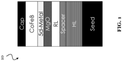
FIG. 1 for an exemplaryVCMA MRAM device 10, a thin transition metal (TM) film, such as a 5d transition-metal film made of iridium (Ir), may be used as an interface layer arranged between an MgO tunnel barrier layer and a magnetic CoFeB free layer. This approach has been shown to be beneficial for increasing the positive magnetoanisotropy energy (MAE), i.e., the perpendicular magneto anisotropy (PMA). However, as a drawback of this approach, the coercive field (Hc) of the free layer is quite low, due to the presence of the Ir at the interface of the free layer. The Hc is the magnetic field that the magnetization of the free layer is able to withstand without becoming demagnetized or even being switched. The reason for the reduced Hc is that the Ir acts as an anti-crystallization barrier, which prevents crystallization to transfer from the MgO layer to the free layer. The low Hc limits the retention of the exemplaryVCMA MRAM device 10. - Additionally, the nature of the TM film induces a change of the electrostatic potential of the VCMA MRAM device stack. Subsequently, a change in the band offset (effective work function of the metals) occurs. The band offset, however, is important to induce an electric field change at the interface, in order to switch the magnetization of the free layer. The band offset that occurs as a consequence of the TM film may thus negatively affect the switching of the magnetization of the free layer by activating more d-orbitals contribution to the negative MAE
- In view of the above, an objective of this disclosure is to provide a new magnetic structure for a VCMA MRAM device, wherein the magnetic structure includes a magnetic free layer and allows increasing the VCMA coefficient ξ to the order of 100 fJ/Vm or even more. At the same time, another objective is to achieve a high coercive field in the free layer, in particular, so that the VCMA MARAM has sufficient retention. Another objective is to enable the magnetization of the free layer to be switched efficiently.
- These and other objectives are achieved by the solutions provided in the enclosed independent claims. Advantageous implementations are further defined in the dependent claims.
- The solutions of this disclosure are based on a magnetic structure including an engineered interface layer, which is provided on the magnetic free layer on one side, and further including an engineered cap layer, which is provided on the free layer on the other side opposite to the engineered interface layer.
- A first aspect of this disclosure provides a magnetic structure for a VCMA MRAM device, the magnetic structure comprising: a magnetic reference layer; a tunnel barrier layer provided directly on the magnetic reference layer; an interface layer provided directly on the tunnel barrier layer; a magnetic free layer provided directly on the interface layer; and a cap layer provided directly on the magnetic free layer; wherein the interface layer and the cap layer are designed to enhance or control an orbital occupancy and/or a spin-orbit coupling of the magnetic free layer.
- The orbital occupancy of the magnetic free layer denotes the electron occupancy of the orbitals of the magnetic free layer material. Spin-orbit-coupling is a well-known physical effect and/or material property. The spin-orbit-coupling of the magnetic free layer accordingly is a material property of the material of the magnetic free layer. An enhanced or controlled orbital occupancy and/or spin-orbit-coupling may be an increased orbital occupancy and/or a stronger spin-orbit-coupling, and may lead to a higher PMA, and may further lead to a larger VCMA coefficient. Thus, the control or enhancement of the orbital occupancy and/or of the spin-orbit-coupling of the magnetic free layer, by properly engineering (i.e., selecting material composition and thickness of) the interface layer and the cap layer, respectively, leads to an increase of the VCMA coefficient of the magnetic structure. In particular, the magnetic structure may have a VCMA coefficient of 100 fJ/Vm or even larger. Notably, the orbital occupancy and/or the spin-orbit-coupling of the free layer of the magnetic structure of the first aspect is particularly controlled or enhanced compared to not having properly engineered interface layer and cap layer, for example, when using an Ir layer as the interface layer and a conventional metal layer (e.g., tantalum layer) as the cap layer, as it is, for example, the case for the
VCMA MRAM device 10 shown inFIG. 2 . - In an implementation of the magnetic structure, the interface layer is designed also to enhance a crystallinity of the magnetic free layer; and/or the cap layer is also designed to terminate a composition of the magnetic free layer.
- That is, the interface layer is also designed to improve a crystallization of the magnetic free layer, i.e., the magnetic free layer has a better crystallization than without the engineered interface layer, or than with an interface layer made from Ir, as it is used in the exemplary
VCMA MRAM device 10 shown inFIG. 2 . In particular, the interface layer of the magnetic structure of the first aspect is also designed to control a termination composition of the magnetic free layer, which leads to the higher crystallinity of the magnetic free layer. - In an implementation of the magnetic structure, the cap layer comprises at least one 4f-metal layer and/or 5d-metal layer configured to enhance or control the orbital occupancy and/or the spin-orbit coupling of the magnetic free layer; and/or the interface layer comprises at least one 4f-metal layer and/or 5d-metal layer configured to enhance or control the orbital occupancy and/or the spin-orbit coupling of the magnetic free layer.
- The proper selection of the cap layer material may increase the crystallization of the magnetic free layer, while it may at the same time also enhance or control the orbital occupancy and/or the spin-orbit coupling.
- In an implementation of the magnetic structure, the interface layer comprises at least one oxide layer configured to enhance the crystallinity of the magnetic free layer; and/or the interface layer comprises a dusting layer made of at least one material, which is also included in the magnetic free layer and is configured to terminate the composition of the magnetic free layer.
- The proper selection of the interface layer material improves not only the crystallization of the magnetic free layer but may also modify the band offset between free layer and tunnel barrier, and may improve the controllability of the orbital occupancy and/or of the spin-orbit coupling of the free layer. As a result, a large VCMA coefficient is achieved.
- In an implementation of the magnetic structure, the cap layer comprises at least one of an oxide layer and a metal layer; the oxide layer comprises at least one of magnesium oxide, magnesium aluminum oxide, and magnesium titanium oxide; and/or the metal layer comprises at least one of iridium, platinum, vanadium, scandium, osmium, gadolinium, terbium, and ytterbium.
- Such a cap layer may be designed to enhance the orbital occupancy and/or the spin-orbit coupling of the magnetic free layer.
- In an implementation of the magnetic structure, the interface layer comprises at least one of an iron layer, a cobalt layer, an iridium layer, a platinum layer, a vanadium layer, a scandium layer, an osmium layer, a gadolinium layer, a terbium layer, and an ytterbium layer.
- Such an interface layer may be designed to enhance or control the orbital occupancy and/or the spin-orbit coupling of the magnetic free layer.
- Accordingly, an alternative aspect of this disclosure provides a magnetic structure for a VCMA MRAM device, the magnetic structure comprising: a magnetic reference layer; a tunnel barrier layer provided directly on the magnetic reference layer; an interface layer provided directly on the tunnel barrier layer; a magnetic free layer provided directly on the interface layer; and a cap layer provided directly on the magnetic free layer; wherein the cap layer comprises at least one of an oxide layer and a metal layer; wherein the oxide layer comprises at least one of magnesium oxide, magnesium aluminum oxide, and magnesium titanium oxide; wherein the metal layer comprises at least one of iridium, platinum, gadolinium, terbium, vanadium, scandium, osmium, and ytterbium; and wherein the interface layer comprises at least one of an iron layer, a cobalt layer, an iridium layer, a platinum layer, an osmium layer, a gadolinium layer, a terbium layer, a vanadium layer, a scandium layer, and an ytterbium layer
- In an implementation of the magnetic structure, the magnetic free layer is doped with a 4f-metal.
- This may further increase the VCMA coefficient, since it may further enhance the orbital occupancy and/or the spin-orbit coupling of the free layer.
- In an implementation of the magnetic structure, the magnetic free layer comprises at least one of cobalt-iron-boron and iron-boron, and is doped with at least one of gadolinium, terbium, and ytterbium.
- Such a magnetic free layer leads to a particularly large VCMA coefficient.
- In an implementation of the magnetic structure, the interface layer has a thickness in a range of 0.1-3 Angstrom; and/or the cap layer has a thickness in a range of 1-5 Angstrom; and/or the magnetic free layer has a thickness in a range of 5-10 Angstrom.
- These advantageous layer thicknesses lead to a particularly large VCMA coefficient.
- In an implementation of the magnetic structure, the interface layer consists of an iridium layer provided directly on the tunnel barrier layer, and an iron layer provided directly on the iridium layer.
- In an implementation of the magnetic structure, the iron layer has a thickness of about 2.5 Angstrom and the iridium layer has a thickness of about 0.5 Angstrom.
- The above implementations provide a specific example of an interface layer, with which VCMA coefficients of above 100 fJ/Vm can be achieved.
- In an implementation of the magnetic structure, the magnetic free layer consists of one of the following: a cobalt-iron-boron layer provided directly on the interface layer; a gadolinium layer provided directly on the interface layer, and a cobalt-iron-boron layer provided directly on the gadolinium layer; a cobalt-iron-boron layer provided directly on the interface layer, a gadolinium layer provided directly on the cobalt-iron-boron layer, and another cobalt-iron-boron layer provided directly on the gadolinium layer.
- In an implementation of the magnetic structure, the cobalt-iron-boron layer of the magnetic free layer is provided directly on the iron layer of the interface layer.
- The above implementations provide a specific example of a magnetic free layer, with which VCMA coefficients of above 100 fJ/Vm can be achieved.
- A second aspect of this disclosure provides a VCMA MRAM device comprising the magnetic structure according to the first aspect or any implementation form thereof.
- In an implementation of the VCMA MRAM device, the VCMA MRAM device further comprises: a spacer layer provided directly on the reference layer on the opposite side of the tunnel barrier layer; a magnetic hard layer provided directly on the spacer layer on the opposite side of the reference layer; and a seed layer provided directly on the magnetic hard layer on the opposite side of the spacer layer.
- By using the magnetic structure of the first aspect, the VCMA MRAM device of the second aspect shows a very large VCMA coefficient, for instance, around 100 fJ/Vm or even more.
- The VCMA MRAM device of the second aspect achieves the same advantages as the magnetic structure of the first aspect and may be extended by respective implementations as described above for the magnetic structure of the first aspect.
- A third aspect of this disclosure provides a method for fabricating a magnetic structure according to the first aspect and/or a VCMA MRAM device according to the second aspect. The method includes steps of fabricating the respective layers of the magnetic structure and/or the VCMA MRAM device.
- The method of the third aspect achieves the same advantages as the magnetic structure of the first aspect and/or the VCMA MRAM device of the second aspect, and may be extended by respective implementations as described above for the magnetic structure of the first aspect.
- The above described aspects and implementations are explained in the following description of embodiments with respect to the enclosed drawings:
- FIG. 1
- shows an example of a VCMA MRAM device.
- FIG. 2
- shows a magnetic structure for a VCMA MRAM device, according to an embodiment of this disclosure.
- FIG. 3
- shows a VCMA MRAM device according to an embodiment of this disclosure.
- FIG. 4
- shows examples of a VCMA MRAM device according to an embodiment of this disclosure.
- FIG. 5
- shows further examples of a VCMA MRAM device according to an embodiment of this disclosure.
- FIG. 6
- compares VCMA coefficients for different exemplary magnetic structures according to embodiments of this disclosure, which have different interface layers.
- FIG. 7
- shows a switching behavior of different exemplary magnetic structures according to embodiments of this disclosure, which have different interface layers.
-
FIG. 2 shows amagnetic structure 20 according to an embodiment of this disclosure. Themagnetic structure 20 can be used to design and build a VCMA MRAM device 30 (see e.g.,FIG. 3 ), which shows a large VCMA coefficient, in particular, of at least 100 fJ/Vm or more. - The
magnetic structure 20 comprises amagnetic reference layer 21, a magnetictunnel barrier layer 22, aninterface layer 23, a magneticfree layer 24, and acap layer 25. - The
magnetic reference layer 21 maybe a cobalt-based layer or an iron-based layer. For example, themagnetic reference layer 21 maybe a CoFeB layer. The magnetic reference layer may have a fixed polarization. - The
tunnel barrier layer 22 is provided directly on themagnetic reference layer 21. Generally in this disclosure, a layer being "provided on" another layer means that this layer is "provided directly on" the other layer. In contrast thereto, a layer "provided above" another layer means that the layer is "provided indirectly on" the other layer, for example, with one or more additional layers arranged in between the layer and the other layer. Thetunnel barrier layer 22 may be a dielectric layer or an oxide layer. For example, thetunnel barrier layer 22 may be an MgO layer. - The
interface layer 23 is provided directly on thetunnel barrier layer 22. Theinterface layer 23 may comprise at least one of an iron (Fe) layer, a cobalt (Co) layer, an Ir layer, a platinum (Pt) layer, an osmium (Os) layer, a gadolinium (Gd) layer, a terbium (Tb) layer, a vanadium (V) layer, a scandium (Sc) layer, an osmium (Os) layer, and an ytterbium (Yt) layer. Theinterface layer 23 may be referred to as a specifically engineered interface layer, which enhances (increases) or controls an orbital occupancy and/or a spin-orbit-coupling of the magnetic free layer 24 (compared to no interface layer or a thin Ir interface layer). To this end, theinterface layer 23 may comprise at least one 4f-metal layer (e.g., of Gd, Tb, and Yb) and/or at least one 5d-metal layer (e.g., Ir, Pt). Notably, only an Ir layer would not enhance the orbital occupancy and/or the spin-orbit-coupling of thefree layer 24, and thus theinterface layer 23 cannot consist only of an Ir layer. - The
interface layer 23 may be further designed to enhance a crystallinity of the magneticfree layer 24. To this end, theinterface layer 23 may comprise at least one oxide layer and/or a dusting layer that is made of at least one material also included in the magnetic free layer 24 (e.g., a dusting layer of Co or Fe in case of a CoFeB free layer) and is configured to terminate the composition of the magneticfree layer 24. As a particular example, theinterface layer 23 may consist of an Ir layer and an iron (Fe) layer, wherein the Ir layer is provided on the tunnel barrier layer and the Fe layer is provided on the Ir layer. - The magnetic
free layer 24 is provided directly on theinterface layer 23. The magneticfree layer 24 may comprise at least one of a CoFeB and an iron-boron (FeB) layer, and may be doped with at least one of gadolinium, terbium, and ytterbium. For example, thefree layer 24 may be doped with a 4f-metal. However, thefree layer 24 may also be undoped. As particular examples, thefree layer 24 may consist of a CoFeB layer, or may consist of a gadolinium (Gd) layer and a CoFeB layer on the Gd layer, or may consist of a Gd layer and two CoFeB layers that sandwich the Gd layer. - The
cap layer 25 is provided directly on the magneticfree layer 24. Thecap layer 25 may comprise at least one of an oxide layer and a metal layer. Thereby, the oxide layer may comprise at least one of MgO, magnesium aluminum oxide (MgAl2O3), and magnesium titanium oxide (MgTiO). The metal layer may comprise at least one of Ir, Pt, Gd, Tb, and Yb. Thecap layer 25 may be referred to as a specifically engineered interface layer, which enhances (increases) or controls the orbital occupancy and/or the spin-orbit-coupling of the magneticfree layer 24. To this end, thecap layer 25 may comprise at least one 4f-metal layer (e.g., Gd, Tb, Yb) and/or 5d-metal layer (e.g., Ir, Pt). Thecap layer 25 may be further designed to terminate a composition of the magneticfree layer 24. To this end, thecap layer 25 may comprise at least one oxide layer (e.g., MgO, MgTiO, MgAl2O3) configured to enhance or control the crystallinity of the magneticfree layer 24. - The
cap layer 25 can particularly be designed to perform a functional role of strain relaxation and/or crystal nucleation in thefree layer 24, in order to enhance the crystallinity of thefree layer 24. For instance, MgO is an often used and thus well available material. MgAl2O3 may provide an improved lattice match between thecap layer 25 and thefree layer 24. MgTiO may be used as a conductive equivalent to MgO. Also a magnetic oxide, like an iron oxide, could be added to thecap layer 25. As particular examples, thecap layer 25 may consist of an MgO layer or may consist of an Ir layer. -
FIG. 3 shows an example of aVCMA MRAM device 30 according to an embodiment of this disclosure. TheVCMA MRAM device 30 includes themagnetic structure 20 shown inFIG. 2 and described in detail above. Same elements inFIG. 2 andFIG. 3 are labelled with the same reference signs, and may be implemented likewise. - In addition to the
magnetic structure 20, theVCMA MRAM device 30 includes aspacer layer 31, a magnetichard layer 32, and aseed layer 33. Thespacer layer 31 is provided directly on thereference layer 21, on the opposite side of thetunnel barrier layer 22. The magnetichard layer 32 is provided directly on thespacer layer 31, on the opposite side of thereference layer 21. Theseed layer 33 is provided directly on the magnetichard layer 32, on the opposite side of thespacer layer 31. -
FIG. 4(a), FIG. 4(b) ,FIG. 5(a), and FIG. 5(b) , show differentVCMA MRAM devices 30 according to embodiments of this disclosure. The shown embodiments are all examples of possible embodiments, and build on the embodiment shown inFIG. 3 . Same elements in theFIGs. 3 ,4 and5 are labelled with the same reference signs, and may be implemented likewise. - In the exemplary
VCMA MRAM device 30 shown inFIG. 4(a) , theinterface layer 23 consists of anIr layer 23a provided directly on the tunnel barrier layer 22 (e.g., MgO), and aFe layer 23b provided directly on theIr layer 23a. TheFe layer 23a may have a thickness of about 2.5 Angstrom and theIr layer 23b may have a thickness of about 0.5 Angstrom. The magneticfree layer 24 is provided on theFe layer 23b, and is a CoFeB layer. Thecap layer 25 may be an MgO layer. - In the exemplary
VCMA MRAM device 30 shown inFIG. 4(b) , theinterface layer 23 consists of anIr layer 23a provided directly on the tunnel barrier layer 22 (e.g., MgO), and aFe layer 23b provided directly on theIr layer 23a. TheFe layer 23a may have a thickness of about 2.5 Angstrom and theIr layer 23b may have a thickness of about 0.5 Angstrom. The magneticfree layer 24 consists of aGd layer 24a, which is provided directly on theFe layer 23b of theinterface layer 23, and aCoFeB layer 24b, which is provided directly on theGd layer 24a. Thecap layer 25 may be an MgO layer. - In the exemplary
VCMA MRAM device 30 shown inFIG. 5(a) , theinterface layer 23 consists of anIr layer 23a provided directly on the tunnel barrier layer 22 (e.g., MgO), and aFe layer 23b provided directly on theIr layer 23a. TheFe layer 23a may have a thickness of about 2.5 Angstrom and theiridium layer 23b may have a thickness of about 0.5 Angstrom. The magneticfree layer 24 consists of aCoFeB layer 24a provided directly on theFe layer 23b of theinterface layer 23, aGd layer 24b provided directly on theCoFeB layer 24a, and anotherCoFeB layer 24c provided directly on theGd layer 24b. Thecap layer 25 may be an MgO layer. - In the exemplary
VCMA MRAM device 30 shown inFIG. 5(b) , theinterface layer 23 consists of anIr layer 23a provided directly on the tunnel barrier layer 22 (e.g., MgO), and aFe layer 23b provided directly on theIr layer 23a. TheFe layer 23a may have a thickness of about 2.5 Angstrom and theIr layer 23b may have a thickness of about 0.5 Angstrom. The magneticfree layer 24 is provided on theFe layer 23b, and is a CoFeB layer. Thecap layer 25 is an Ir layer and may have a thickness of about 5 Angstrom. -
FIG. 6 compares VCMA coefficients achieved for differentmagnetic structures 20 in (a), (b), (d) and (e) suitable forVCMA MRAM devices 30. The differentmagnetic structures 20 each include the magnetic free layer 24 (here a 30% CoFeB wedge is used), the interface layer 23 (a different kind is used for each magnetic structure 20), the tunnel barrier layer (here MgO is used), the reference layer 21 (here CoFeB is used), and the cap layer 25 (here MgO is used). - In particular,
FIG. 6 compares the differentmagnetic structure 20 with a process of record (POR), i.e., a reference magnetic structure, in (c). In particular, the reference magnetic structure has a CoFeB reference layer, an MgO tunnel barrier layer on the reference layer, a CoFeB free layer on the MgO tunnel barrier layer, and a tantalum (Ta) cap layer. - The different
magnetic structures 20 evaluated inFIG. 6 particularly comprise the following interface layers 23: (a) aninterface layer 23 consisting of a 0.5 Angstrom Ir layer on thetunnel barrier layer 22 and a 2.5 Angstrom Co layer provided on the Ir layer; (b) a 2.5 Angstrom Co layer on thetunnel barrier layer 22 and a 0.5 Angstrom Ir layer provided on the Co layer; (d) aninterface layer 23 consisting of a 0.5 Angstrom Fe layer on thetunnel barrier layer 22 and a 0.5 Angstrom Ir layer provided on the Fe layer; and (e) aninterface layer 23 consisting of a 1.0 Angstrom Ir layer on thetunnel barrier layer 22 and a 0.5 Angstrom Fe layer provided on the Ir layer. - For each of the interface layers 23, several data points are shown in
FIG. 6 . The data points are taken for different thicknesses of the CoFeBfree layer 24, wherein this thickness is shown on the x-axis. The VCMA coefficients are shown on the y-axis (in fJ/Vm) in the upper part of the result table. In addition, also dHk/dEF is shown on the y-axis (in mT∗nm/V) in the lower part of the result table. Thereby, Hk is the anisotropy field (or PMA filed) of themagnetic structure 20, and EF is the voltage-induced electric field that is applied to themagnetic structure 20 for switching the magneticfree layer 24. A high dHk/dEF is required to have a large VCMA coefficient. The VCMA coefficient can, in particular, be calculated by (dHk/dEF)∗(Ms∗t), wherein Ms is the saturation magnetization and t is the thickness of thefree layer 24. For example, dHk/dEF can be estimated from electrical analysis, and Ms∗t can be estimated from material analysis. - For each
interface layer 23 evaluated inFIG. 6 , the VCMA coefficient of the magnetic structure 20 - which is based on a full perpendicular magnetic tunnel junction (MTJ) structure - is larger than the VCMA coefficient of the POR at the same thickness of the free layer. For the "best" free layer thickness, the VCMA coefficients are in the order of 100 fJ/Vm, or are 100 fJ/Vm, or are even more than 100 fJ/Vm. In particular, for the Ir/Fe interface layer 23 and for the Fe/Ir interface layer 23, the VCMA coefficient reach the highest values well above 100 fJ/Vm. - At the same time, in addition to the large VCMA coefficients, for each
interface layer 23 evaluated inFIG. 6 , the coercive field is clearly higher than the coercive field in the POR. This can, for example, be derived from the comparison of the voltage-induced anisotropy field change dHk/dEF of themagnetic structure 20 compared to the reference magnetic structure (POR). - Further, for each
interface layer 23 evaluated inFIG. 6 , an efficient VCMA induced magnetization switching can be observed, as exemplarily shown inFIG. 7 for two specific interface layers 23. In particular,FIG. 7 evaluates (a) aninterface layer 23 consisting of a 0.5 Angstrom Ir layer on thetunnel barrier layer 22 and a 2.5 Angstrom Fe layer on the Ir layer; and (b) aninterface layer 23 consisting of a 0.5 Angstrom Ir layer on thetunnel barrier layer 22 and a 2.5 Angstrom Co layer on the Ir layer (compare (a) inFIG. 6 ). It is clearly demonstrated that the switching of the magnetization of the magneticfree layer 24 from anti-parallel to parallel and from parallel to anti-parallel (compared to the magnetization of the reference layer 21) is well possible. Notably, for testing the magnetization switching, voltage pulses are applied to themagnetic structures 20, and at the same time a magnetic field is applied. The voltage-induced electric field (EF) that results from the amplitude of the applied voltage pulse is -1.33 V/m in both cases, and the applied magnetic field is 20 mT in (a) and 35 mT in (b). The applied voltage pulses have different pulse width between o ns and 2 ns (see the x-axis ofFIG. 7(a) and FIG. 7(b) ), and the corresponding switching probability (Psw in %) is shown (on the y-axis ofFIG. 7(a) and FIG. 7(b) ). - In summary, the solutions of this disclosure enable increasing the VCMA coefficient of a
magnetic structure 20 and a VCMA MRAM device, respectively, to 100 fJ/Vm or more. This increase is achieved by engineering theinterface layer 23 and thecap layer 25 that sandwich thefree layer 23. Thereby, engineering includes selecting the material(s) and the thicknesses of these layers. The engineered layers enhance the orbital occupancy and/or the spin-orbit-coupling of thefree layer 24, and may further provide extra crystallinity to the magneticfree layer 24 and/or boost both the band offset and the Hc in thefree layer 24.
Claims (15)
- A magnetic structure (20) for a voltage controlled magnetic anisotropy, VCMA, magnetic random access memory, MRAM, device (30), the magnetic structure (20) comprising:a magnetic reference layer (21);a tunnel barrier layer (22) provided directly on the magnetic reference layer (21);an interface layer (23) provided directly on the tunnel barrier layer (22);a magnetic free layer (24) provided directly on the interface layer (23); anda cap layer (25) provided directly on the magnetic free layer (24);wherein the interface layer (23) and the cap layer (25) are designed to enhance an orbital occupancy and/or a spin-orbit-coupling of the magnetic free layer (24).
- The magnetic structure (20) according to claim 1, whereinthe interface layer (23) is also designed to enhance a crystallinity of the magnetic free layer (24); and/orthe cap layer (25) is also designed to terminate a composition of the magnetic free layer (24).
- The magnetic structure (20) according to claim 1 or 2, wherein:the cap layer (25) comprises at least one 4f-metal layer and/or 5d-metal layer configured to control the orbital occupancy and/or the spin-orbit coupling of the magnetic free layer (24); and/orthe interface layer (23) comprises at least one 4f-metal layer and/or 5d-metal layer configured to enhance the orbital occupancy and/or the spin-orbit coupling of the magnetic free layer (24).
- The magnetic structure (20) according to claim 2 or 3, wherein:the interface layer (23) comprises at least one oxide layer configured to enhance the crystallinity of the magnetic free layer (24); and/orthe interface layer (23) comprises a dusting layer made of at least one material, which is also included in the magnetic free layer (24) and is configured to terminate the composition of the magnetic free layer (24).
- The magnetic structure (20) according to one of the claims 1 to 4, wherein:the cap layer (25) comprises at least one of an oxide layer and a metal layer;the oxide layer comprises at least one of magnesium oxide, magnesium aluminum oxide, and magnesium titanium oxide; and/orthe metal layer comprises at least one of iridium, platinum, osmium, gadolinium, terbium, vanadium, scandium, and ytterbium.
- The magnetic structure (20) according to one of the claims 1 to 5, wherein the interface layer (23) comprises at least one of an iron layer, a cobalt layer, an iridium layer, a platinum layer, an osmium layer, a gadolinium layer, a terbium layer, a vanadium layer, a scandium layer and an ytterbium layer.
- The magnetic structure (20) according to one of the claims 1 to 6, wherein the magnetic free layer (24) is doped with a 4f-metal.
- The magnetic structure (20) according to one of the claims 1 to 7, wherein the magnetic free layer (24) comprises at least one of cobalt-iron-boron and iron-boron, and is doped with at least one of gadolinium, terbium, and ytterbium.
- The magnetic structure (20) according to one of the claims 5 to 8, wherein:the interface layer (23) has a thickness in a range of 0.1-3 Angstrom; and/orthe cap layer (25) has a thickness in a range of 1-5 Angstrom; and/orthe magnetic free layer (24) has a thickness in a range of 5-20 Angstrom.
- The magnetic structure (20) according to one of the claims 1 to 9, wherein the interface layer (23) consists of an iridium layer (23a) provided directly on the tunnel barrier layer (22), and an iron layer (23b) provided directly on the iridium layer (23a).
- The magnetic structure (20) according to claim 10, wherein the iron layer (23a) has a thickness of about 2.5 Angstrom and the iridium layer (23b) has a thickness of about 0.5 Angstrom.
- The magnetic structure (20) according to one of the claims 1 to 11, wherein the magnetic free layer (24) consists of one of the following:a cobalt-iron-boron layer provided directly on the interface layer (23);a gadolinium layer (24a) provided directly on the interface layer (23), and a cobalt-iron-boron layer (24b) provided directly on the gadolinium layer (24a);a cobalt-iron-boron layer (24a) provided directly on the interface layer (23), a gadolinium layer (24b) provided directly on the cobalt-iron-boron layer (24a), and another cobalt-iron-boron layer (24c) provided directly on the gadolinium layer (24b).
- The magnetic structure (20) according to claim 12 and according to claim 10 or 11, wherein the cobalt-iron-boron layer (24, 24a) of the magnetic free layer (24) is provided directly on the iron layer (23b) of the interface layer (23).
- A VCMA MRAM device (30) comprising the magnetic structure (20) according to any one of the claims 1 to 13.
- The VCMA MRAM device (30) according to claim 14, wherein the VCMA MRAM device (30) further comprises:a spacer layer (31) provided directly on the reference layer (21) on the opposite side of the tunnel barrier layer (22);a magnetic hard layer (32) provided directly on the spacer layer (31) on the opposite side of the reference layer (21); anda seed layer (33) provided directly on the magnetic hard layer (32) on the opposite side of the spacer layer (31).
Priority Applications (2)
| Application Number | Priority Date | Filing Date | Title |
|---|---|---|---|
| EP21213085.0A EP4195206A1 (en) | 2021-12-08 | 2021-12-08 | A free-layer design for a voltage control of magnetic anisotropy magnetic random access memory device |
| US18/062,785 US12462859B2 (en) | 2021-12-08 | 2022-12-07 | Free-layer design for a voltage control of magnetic anisotropy magnetic random access memory device |
Applications Claiming Priority (1)
| Application Number | Priority Date | Filing Date | Title |
|---|---|---|---|
| EP21213085.0A EP4195206A1 (en) | 2021-12-08 | 2021-12-08 | A free-layer design for a voltage control of magnetic anisotropy magnetic random access memory device |
Publications (1)
| Publication Number | Publication Date |
|---|---|
| EP4195206A1 true EP4195206A1 (en) | 2023-06-14 |
Family
ID=78824721
Family Applications (1)
| Application Number | Title | Priority Date | Filing Date |
|---|---|---|---|
| EP21213085.0A Pending EP4195206A1 (en) | 2021-12-08 | 2021-12-08 | A free-layer design for a voltage control of magnetic anisotropy magnetic random access memory device |
Country Status (2)
| Country | Link |
|---|---|
| US (1) | US12462859B2 (en) |
| EP (1) | EP4195206A1 (en) |
Families Citing this family (1)
| Publication number | Priority date | Publication date | Assignee | Title |
|---|---|---|---|---|
| US12320870B2 (en) * | 2022-07-19 | 2025-06-03 | Allegro Microsystems, Llc | Controlling out-of-plane anisotropy in an MR sensor with free layer dusting |
Citations (2)
| Publication number | Priority date | Publication date | Assignee | Title |
|---|---|---|---|---|
| US20190189908A1 (en) * | 2017-12-20 | 2019-06-20 | Inston Inc. | Heterostructures for Electric Field Controlled Magnetic Tunnel Junctions |
| US20210210676A1 (en) * | 2019-11-22 | 2021-07-08 | Western Digital Technologies, Inc., | Magnetoresistive memory device including a magnesium containing dust layer |
Family Cites Families (8)
| Publication number | Priority date | Publication date | Assignee | Title |
|---|---|---|---|---|
| WO2012159078A2 (en) | 2011-05-19 | 2012-11-22 | The Regents Of The University Of California | Voltage-controlled magnetic anisotropy (vcma) switch and magneto-electric memory (meram) |
| US9589619B2 (en) | 2015-02-09 | 2017-03-07 | Qualcomm Incorporated | Spin-orbit-torque magnetoresistive random access memory with voltage-controlled anisotropy |
| US9978931B2 (en) | 2015-02-13 | 2018-05-22 | Inston Inc. | Systems and methods for implementing robust magnetoelectric junctions |
| US9680089B1 (en) | 2016-05-13 | 2017-06-13 | Micron Technology, Inc. | Magnetic tunnel junctions |
| JP6509971B2 (en) | 2017-08-08 | 2019-05-08 | 株式会社東芝 | Magnetic storage element and magnetic storage device |
| US11114605B2 (en) * | 2018-08-12 | 2021-09-07 | HeFeChip Corporation Limited | Composite storage layer for magnetic random access memory devices |
| TWI751728B (en) * | 2020-10-07 | 2022-01-01 | 財團法人工業技術研究院 | In-plane magnetized spin-orbit magnetic device |
| US11887640B2 (en) * | 2021-06-07 | 2024-01-30 | Western Digital Technologies, Inc. | Voltage-controlled magnetic anisotropy memory device including an anisotropy-enhancing dust layer and methods for forming the same |
-
2021
- 2021-12-08 EP EP21213085.0A patent/EP4195206A1/en active Pending
-
2022
- 2022-12-07 US US18/062,785 patent/US12462859B2/en active Active
Patent Citations (2)
| Publication number | Priority date | Publication date | Assignee | Title |
|---|---|---|---|---|
| US20190189908A1 (en) * | 2017-12-20 | 2019-06-20 | Inston Inc. | Heterostructures for Electric Field Controlled Magnetic Tunnel Junctions |
| US20210210676A1 (en) * | 2019-11-22 | 2021-07-08 | Western Digital Technologies, Inc., | Magnetoresistive memory device including a magnesium containing dust layer |
Non-Patent Citations (1)
| Title |
|---|
| LI XIANG: "Interface Engineering of Voltage-Controlled Embedded Magnetic Random Access Memory", 1 January 2018 (2018-01-01), XP055927502, Retrieved from the Internet <URL:https://escholarship.org/content/qt2t0089x7/qt2t0089x7_noSplash_af5b956798555a1cf7983195f3816ef3.pdf> [retrieved on 20220602] * |
Also Published As
| Publication number | Publication date |
|---|---|
| US20230178131A1 (en) | 2023-06-08 |
| US12462859B2 (en) | 2025-11-04 |
Similar Documents
| Publication | Publication Date | Title |
|---|---|---|
| US11527261B2 (en) | Storage element | |
| KR102078595B1 (en) | Method and system for providing an engineered magnetic layer including heusler layers and an amorphous insertion layer | |
| KR102145269B1 (en) | Dual perpendicular magnetic anisotropy magnetic junction usable in spin transfer torque magnetic random access memory applications | |
| EP2718928B1 (en) | Spin-torque magnetoresistive memory element and method of fabricating same | |
| US8637947B2 (en) | Memory element and memory apparatus | |
| US7283386B2 (en) | Voltage-controlled magnetization reversal writing type magnetic random access memory device and method of writing and reading information using the same | |
| US20140374752A1 (en) | Perpendicular magnetization storage element and storage device | |
| KR102188529B1 (en) | Method and system for providing a bulk perpendicular magnetic anisotropy free layer in a perpendicular magnetic junction usable in spin transfer torque magnetic random access memory applications | |
| KR102684723B1 (en) | Magnetic apparatus having magnetic junctions and hybrid capping layers, magnetic memory using the same, and method for providing the same | |
| US9818932B2 (en) | Storage element, storage device, and magnetic head | |
| JP2011129933A (en) | Perpendicular magnetic tunnel junction structure and magnetic element including the same, and method of manufacturing the same | |
| KR20150054665A (en) | Method and system for providing a top pinned layer perpendicular magnetic anisotropy magnetic junction usable in spin transfer torque magnetic random access memory applications | |
| US9287322B2 (en) | Method for controlling magnetic properties through ion diffusion in a magnetic junction usable in spin transfer torque magnetic random access memory applications | |
| KR20100131967A (en) | Driving method of ferromagnetic tunnel junction element and ferromagnetic tunnel junction element | |
| US20140169087A1 (en) | Memory element and memory apparatus | |
| KR20160004959A (en) | Method and system for providing rare earth magnetic junctions usable in spin transfer torque magnetic random access memory applications | |
| KR20190104864A (en) | Magnetic junction, method for providing the same, and magnetic memory | |
| CN103137853A (en) | Memory element and memory apparatus | |
| US20230178131A1 (en) | Free-layer Design for a Voltage Control of Magnetic Anisotropy Magnetic Random Access Memory Device | |
| US10069062B2 (en) | Magnetoresistive element | |
| KR20190024545A (en) | A magnetic junction, a magnetic memory using the same, and a method for providing the magnetic junction | |
| CN120265104A (en) | MTJ structure and magnetic random access memory |
Legal Events
| Date | Code | Title | Description |
|---|---|---|---|
| PUAI | Public reference made under article 153(3) epc to a published international application that has entered the european phase |
Free format text: ORIGINAL CODE: 0009012 |
|
| STAA | Information on the status of an ep patent application or granted ep patent |
Free format text: STATUS: THE APPLICATION HAS BEEN PUBLISHED |
|
| AK | Designated contracting states |
Kind code of ref document: A1 Designated state(s): AL AT BE BG CH CY CZ DE DK EE ES FI FR GB GR HR HU IE IS IT LI LT LU LV MC MK MT NL NO PL PT RO RS SE SI SK SM TR |
|
| STAA | Information on the status of an ep patent application or granted ep patent |
Free format text: STATUS: REQUEST FOR EXAMINATION WAS MADE |
|
| 17P | Request for examination filed |
Effective date: 20231211 |
|
| RBV | Designated contracting states (corrected) |
Designated state(s): AL AT BE BG CH CY CZ DE DK EE ES FI FR GB GR HR HU IE IS IT LI LT LU LV MC MK MT NL NO PL PT RO RS SE SI SK SM TR |