EP4195194A1 - Mini led driving power source and mini led television - Google Patents
Mini led driving power source and mini led television Download PDFInfo
- Publication number
- EP4195194A1 EP4195194A1 EP21951718.2A EP21951718A EP4195194A1 EP 4195194 A1 EP4195194 A1 EP 4195194A1 EP 21951718 A EP21951718 A EP 21951718A EP 4195194 A1 EP4195194 A1 EP 4195194A1
- Authority
- EP
- European Patent Office
- Prior art keywords
- resistor
- capacitor
- power supply
- voltage
- another end
- Prior art date
- Legal status (The legal status is an assumption and is not a legal conclusion. Google has not performed a legal analysis and makes no representation as to the accuracy of the status listed.)
- Pending
Links
Images





Classifications
-
- G—PHYSICS
- G09—EDUCATION; CRYPTOGRAPHY; DISPLAY; ADVERTISING; SEALS
- G09G—ARRANGEMENTS OR CIRCUITS FOR CONTROL OF INDICATING DEVICES USING STATIC MEANS TO PRESENT VARIABLE INFORMATION
- G09G3/00—Control arrangements or circuits, of interest only in connection with visual indicators other than cathode-ray tubes
- G09G3/20—Control arrangements or circuits, of interest only in connection with visual indicators other than cathode-ray tubes for presentation of an assembly of a number of characters, e.g. a page, by composing the assembly by combination of individual elements arranged in a matrix no fixed position being assigned to or needed to be assigned to the individual characters or partial characters
-
- G—PHYSICS
- G09—EDUCATION; CRYPTOGRAPHY; DISPLAY; ADVERTISING; SEALS
- G09G—ARRANGEMENTS OR CIRCUITS FOR CONTROL OF INDICATING DEVICES USING STATIC MEANS TO PRESENT VARIABLE INFORMATION
- G09G3/00—Control arrangements or circuits, of interest only in connection with visual indicators other than cathode-ray tubes
- G09G3/20—Control arrangements or circuits, of interest only in connection with visual indicators other than cathode-ray tubes for presentation of an assembly of a number of characters, e.g. a page, by composing the assembly by combination of individual elements arranged in a matrix no fixed position being assigned to or needed to be assigned to the individual characters or partial characters
- G09G3/34—Control arrangements or circuits, of interest only in connection with visual indicators other than cathode-ray tubes for presentation of an assembly of a number of characters, e.g. a page, by composing the assembly by combination of individual elements arranged in a matrix no fixed position being assigned to or needed to be assigned to the individual characters or partial characters by control of light from an independent source
- G09G3/3406—Control of illumination source
-
- G—PHYSICS
- G09—EDUCATION; CRYPTOGRAPHY; DISPLAY; ADVERTISING; SEALS
- G09G—ARRANGEMENTS OR CIRCUITS FOR CONTROL OF INDICATING DEVICES USING STATIC MEANS TO PRESENT VARIABLE INFORMATION
- G09G3/00—Control arrangements or circuits, of interest only in connection with visual indicators other than cathode-ray tubes
- G09G3/20—Control arrangements or circuits, of interest only in connection with visual indicators other than cathode-ray tubes for presentation of an assembly of a number of characters, e.g. a page, by composing the assembly by combination of individual elements arranged in a matrix no fixed position being assigned to or needed to be assigned to the individual characters or partial characters
- G09G3/34—Control arrangements or circuits, of interest only in connection with visual indicators other than cathode-ray tubes for presentation of an assembly of a number of characters, e.g. a page, by composing the assembly by combination of individual elements arranged in a matrix no fixed position being assigned to or needed to be assigned to the individual characters or partial characters by control of light from an independent source
- G09G3/3406—Control of illumination source
- G09G3/3413—Details of control of colour illumination sources
-
- H—ELECTRICITY
- H05—ELECTRIC TECHNIQUES NOT OTHERWISE PROVIDED FOR
- H05B—ELECTRIC HEATING; ELECTRIC LIGHT SOURCES NOT OTHERWISE PROVIDED FOR; CIRCUIT ARRANGEMENTS FOR ELECTRIC LIGHT SOURCES, IN GENERAL
- H05B45/00—Circuit arrangements for operating light-emitting diodes [LED]
- H05B45/30—Driver circuits
- H05B45/355—Power factor correction [PFC]; Reactive power compensation
-
- G—PHYSICS
- G09—EDUCATION; CRYPTOGRAPHY; DISPLAY; ADVERTISING; SEALS
- G09G—ARRANGEMENTS OR CIRCUITS FOR CONTROL OF INDICATING DEVICES USING STATIC MEANS TO PRESENT VARIABLE INFORMATION
- G09G2310/00—Command of the display device
- G09G2310/02—Addressing, scanning or driving the display screen or processing steps related thereto
- G09G2310/0237—Switching ON and OFF the backlight within one frame
-
- G—PHYSICS
- G09—EDUCATION; CRYPTOGRAPHY; DISPLAY; ADVERTISING; SEALS
- G09G—ARRANGEMENTS OR CIRCUITS FOR CONTROL OF INDICATING DEVICES USING STATIC MEANS TO PRESENT VARIABLE INFORMATION
- G09G2330/00—Aspects of power supply; Aspects of display protection and defect management
- G09G2330/02—Details of power systems and of start or stop of display operation
- G09G2330/021—Power management, e.g. power saving
-
- G—PHYSICS
- G09—EDUCATION; CRYPTOGRAPHY; DISPLAY; ADVERTISING; SEALS
- G09G—ARRANGEMENTS OR CIRCUITS FOR CONTROL OF INDICATING DEVICES USING STATIC MEANS TO PRESENT VARIABLE INFORMATION
- G09G2330/00—Aspects of power supply; Aspects of display protection and defect management
- G09G2330/02—Details of power systems and of start or stop of display operation
- G09G2330/028—Generation of voltages supplied to electrode drivers in a matrix display other than LCD
-
- G—PHYSICS
- G09—EDUCATION; CRYPTOGRAPHY; DISPLAY; ADVERTISING; SEALS
- G09G—ARRANGEMENTS OR CIRCUITS FOR CONTROL OF INDICATING DEVICES USING STATIC MEANS TO PRESENT VARIABLE INFORMATION
- G09G3/00—Control arrangements or circuits, of interest only in connection with visual indicators other than cathode-ray tubes
- G09G3/20—Control arrangements or circuits, of interest only in connection with visual indicators other than cathode-ray tubes for presentation of an assembly of a number of characters, e.g. a page, by composing the assembly by combination of individual elements arranged in a matrix no fixed position being assigned to or needed to be assigned to the individual characters or partial characters
- G09G3/22—Control arrangements or circuits, of interest only in connection with visual indicators other than cathode-ray tubes for presentation of an assembly of a number of characters, e.g. a page, by composing the assembly by combination of individual elements arranged in a matrix no fixed position being assigned to or needed to be assigned to the individual characters or partial characters using controlled light sources
- G09G3/30—Control arrangements or circuits, of interest only in connection with visual indicators other than cathode-ray tubes for presentation of an assembly of a number of characters, e.g. a page, by composing the assembly by combination of individual elements arranged in a matrix no fixed position being assigned to or needed to be assigned to the individual characters or partial characters using controlled light sources using electroluminescent panels
- G09G3/32—Control arrangements or circuits, of interest only in connection with visual indicators other than cathode-ray tubes for presentation of an assembly of a number of characters, e.g. a page, by composing the assembly by combination of individual elements arranged in a matrix no fixed position being assigned to or needed to be assigned to the individual characters or partial characters using controlled light sources using electroluminescent panels semiconductive, e.g. using light-emitting diodes [LED]
-
- H—ELECTRICITY
- H05—ELECTRIC TECHNIQUES NOT OTHERWISE PROVIDED FOR
- H05B—ELECTRIC HEATING; ELECTRIC LIGHT SOURCES NOT OTHERWISE PROVIDED FOR; CIRCUIT ARRANGEMENTS FOR ELECTRIC LIGHT SOURCES, IN GENERAL
- H05B45/00—Circuit arrangements for operating light-emitting diodes [LED]
- H05B45/30—Driver circuits
- H05B45/37—Converter circuits
- H05B45/3725—Switched mode power supply [SMPS]
- H05B45/39—Circuits containing inverter bridges
Definitions
- the present application generally relates to the technical field of power supply, and more particularly, to a MINI LED driving power supply and a MINI LED television.
- Mini-LED television adopts a light source smaller than conventional LED in volume.
- a width of a Mini-LED is about 200 microns, which is one fifth of a size of a standard LED used in an LCD panel. Since a volume of Mini-LED is small enough, it is possible to arrange more Mini-LEDs on an entire screen. When a screen has enough number of LED backlight, it will be possible to better control a bright and dark, a color gradation and more of a picture, so as to provide a better image quality.
- the power supply In order to provide a high quality image, in a design of the power supply of Mini-LED television, the power supply has a higher requirement on a ripple of output voltage, and a precision of the output voltage.
- the objective of the present application is to provide a MINI LED driving power supply and a MINI LED television, which are able to solve a problem in the prior art of different voltages affecting each other during a high power output.
- the first conversion module comprises a standby control unit and a first conversion unit
- the second conversion module comprises an enabling switching unit and a second conversion unit
- the standby control unit comprises a standby switching subunit and a step-down subunit;
- the first conversion unit comprises a conversion subunit and a power supply subunit
- the second conversion unit comprises a main LLC circuit and a main LLC transformer
- the enabling switching unit comprises a first diode, a second diode, a first resistor, a second resistor, a third resistor, a fourth resistor, a fifth resistor, a sixth resistor, a first triode, a second triode, a first capacitor, a second capacitor, a first Zener diode, and a first optocoupler; an anode of the first diode is connected to an enable signal input terminal, an anode of the second diode is connected to an LED_ON signal terminal, both a cathode of the first diode and a cathode of the second diode are connected to one end of the first resistor; another end of the first resistor, one end of the second resistor, and one end of the first capacitor are all connected to a base of the first triode; an emitter of the first triode, another end of the first capacitor, and another end of the second resistor are all grounded; a collector of the first triode is connected to
- the standby switching subunit comprises a third diode, a seventh resistor, an eighth resistor, a ninth resistor, a tenth resistor, a third triode, a third capacitor, and a second optocoupler; an anode of the third diode is connected to the mainboard, a cathode of the third diode is connected to one end of the seventh resistor, another end of the seventh resistor, one end of the eighth resistor, and one end of the third capacitor are all connected to a base of the third triode, an emitter of the third triode, another end of the third capacitor, and another end of the eighth resistor are all grounded; a collector of the third triode is connected to a second pin of the second optocoupler, a first pin of the second optocoupler is connected to the first voltage input terminal through the ninth resistor, a third pin of the second optocoupler is connected to an Auto_stb signal terminal, and a fourth pin of the second optocoupler is
- the step-down subunit comprises a fourth diode, an eleventh resistor, a twelfth resistor, a fourth capacitor, a fourth triode, a thirteenth resistor, a fourteenth resistor, a fifteenth resistor, a sixteenth resistor, a seventeenth resistor, an eighteenth resistor, a nineteenth resistor, a twentieth resistor, a twenty-first resistor, a twenty-second resistor, a twenty-third resistor, a fifth capacitor, a sixth capacitor, a seventh capacitor, an eighth capacitor, a ninth capacitor, a voltage regulator, a third optocoupler, and a second Zener diode;
- An anode of the fourth diode is connected to the mainboard, a cathode of the fourth diode is connected to one end of the eleventh resistor, another end of the eleventh resistor, one end of the twelfth resistor, and one end of the fourth capacitor are all connected to a base of the fourth triode, an emitter of the fourth triode, another end of the fourth capacitor, and another end of the twelfth resistor are all grounded, a collector of the fourth triode is connected to one end of the thirteenth resistor, another end of the thirteenth resistor is connected to one end of the fourteenth resistor, another end of the fourteenth resistor is connected to one end of the fifteenth resistor, one end of the seventh capacitor, one end of the sixth capacitor, one end of the fifth capacitor, and one end of the eighteenth resistor; one end of the seventeenth resistor, one end of the eighth capacitor and one end of the twentieth resistor are all connected to one end of the fifth capacitor, a first pin of the voltage regulator is connected to one end
- a MINI LED television which comprises the MINI LED driving power supply stated above.
- the present application provides a MINI LED driving power supply and a MINI LED television
- the MINI LED driving power supply comprises a power supply board connecting with a mainboard and a MINI LED screen
- the power supply board comprises a first conversion module and a second conversion module
- the first conversion module connects to the mainboard and the second conversion module, applied to outputting a power supply voltage to power the mainboard after the first conversion module is turned on, and outputting a first voltage and a second voltage to power the mainboard according to a power-on/off signal output by the mainboard, as well as outputting a first power supply and a high-voltage direct current to the second conversion module
- the second conversion module connects to the MINI LED screen, applied to converting the high-voltage direct current into a third voltage before outputting to the MINI LED screen according to an enable signal output by the mainboard and the first power supply, to light up the MINI LED screen.
- the present application provides a MINI LED driving power supply and a MINI LED television, being able to solve a problem of different voltages affect each other during a high power output.
- the MINI LED driving power provided by the present application can further be applied to a plurality of display-related power driving including an OLED monitor, an LED monitor, an audiovisual education, and a rear-projection plasma.
- the present application provides a MIN LED driving power supply, which comprises a power supply board connecting with a mainboard 10 and a MINI LED screen 20, the power supply board comprises a first conversion module 31 and a second conversion module 32; the first conversion module 31 connects to the mainboard 10 and the second conversion module 32, applied to outputting a power supply voltage to power the mainboard 10 after the first conversion module 31 is powered on, and outputting a first voltage (+12V in the present embodiment) and a second voltage (+20V in the present embodiment) to power the mainboard 10 according to a power-on/off signal (ON_OFF in the present embodiment) output by the mainboard 10, as well as outputting a first power supply and a high-voltage direct current to the second conversion module 32; the second conversion module 32 connects to the MINI LED screen, applied to converting the high-voltage direct current into a third voltage (+28V in the present embodiment) before outputting to the MINI LED screen 20 according to an enable signal output by the mainboard 10 and the first power supply, to light
- the present application by converting and outputting the first voltage and the third voltage independently, and providing the third voltage to power the screen independently, makes that, whether an output of the third voltage works normally or not will not affect a working state of another line, thus a problem of an interference between a plurality of lines is avoided.
- the first conversion module 31 comprises a standby control unit (not shown in the FIGs) and a first conversion unit (not shown in the drawings), the first conversion unit connects to the mainboard 10, applied to outputting the power supply voltage (10V in the present embodiment) to power the mainboard 10 after first conversion unit is powered on, the standby control unit connects to the mainboard 10 and the first conversion unit respectively, applied to controlling the first conversion unit to start according to the power-on/off signal output by the mainboard 10; the first conversion unit is further applied to outputting the first voltage and the second voltage to power the mainboard 10 after the first conversion unit started, and outputting the high-voltage direct current and the first power supply to the second conversion module 32.
- the first conversion unit connects to the mainboard 10, applied to outputting the power supply voltage (10V in the present embodiment) to power the mainboard 10 after first conversion unit is powered on
- the standby control unit connects to the mainboard 10 and the first conversion unit respectively, applied to controlling the first conversion unit to start according to the power-on/off signal output by the mainboard
- the power supply board After connecting to an AC power, the power supply board outputs 10V to power the mainboard 10, and the mainboard 10 sends a power-on/off signal to the power supply board after working normally, making the power supply board output the first voltage to power the main board 10.
- the mainboard 10 After the mainboard 10 works steadily, it facilitates to control a follow-up work of the second conversion module 32, making the second conversion module 32 output the third voltage to the MINI LED screen 20, and further control the MINI LED screen 20 light up.
- the second conversion module 32 comprises an enabling switching unit 321 and a second conversion unit 322; the enabling switching unit 321 connects to the first converting unit and the second converting unit 322 respectively, applied to converting the first power supply (PWM_VCC in the present embodiment) into a second power supply (VCC_27V in the present embodiment) before outputting to the second conversion unit 322 according to the enable signal output by the mainboard 10; the second conversion unit 322 connects to the MINI LED screen 20, applied to converting the high-voltage direct current into the third voltage to power the MINI LED screen 20 according to the second power supply, further achieving lighting up the MINI LED screen 20.
- the enabling switching unit 321 connects to the first converting unit and the second converting unit 322 respectively, applied to converting the first power supply (PWM_VCC in the present embodiment) into a second power supply (VCC_27V in the present embodiment) before outputting to the second conversion unit 322 according to the enable signal output by the mainboard 10; the second conversion unit 322 connects to the
- the voltage outputs of the first conversion module 31 and the second conversion module 32 are independent of each other, and a voltage output of one line will not interfere with a voltage output of another line, thereby a problem of an interference between lines is avoided effectively. Due to an output of each line is separated completely, when a load of one line changes, there is no affect on an output of another line, which ensures a normal and stable operation of a system.
- the output voltages of the power supply board are independent, making a whole machine work stably and normally, which is able to improve an electric performance of a product, improve a picture quality experience of the MINI LED television and prolong a service life of the screen.
- the standby control unit comprises a standby switching subunit 311 and a step-down subunit 312;
- the standby switching subunit 311 connects to the mainboard 10 and the first conversion unit respectively, applied to controlling the first conversion unit to start according to a power-on/off signal output by the mainboard 10;
- the step-down subunit 312 connects to the mainboard 10 and the first conversion unit respectively, applied to providing a feedback signal for the first conversion unit according to the power-on/off signal.
- the standby switching subunit 311 After receiving a power-on/off signal in a high level, the standby switching subunit 311 exits a standby mode and wakes up the first conversion unit, making the first conversion unit exit the standby mode and enter a working mode.
- the step-down subunit 312 also provides a feedback signal to the first conversion unit according to the power-on/off signal in the high level, making the first conversion unit work normally and output the first voltage and the second voltage to power the mainboard 10, thereby ensuring a stable operation of the mainboard 10.
- the first conversion unit comprises a conversion subunit 3121 and a power supply subunit 3122; the conversion subunit 3121 connects to the power supply subunit 3122 and the mainboard 10 respectively, applied to outputting the power supply voltage to power the mainboard 10 after the conversion subunit 3121 is powered on, and outputting the first voltage and the second voltage to power the mainboard 10 after the conversion subunit 3121 is started, as well as outputting the high-voltage direct current to the second conversion unit 322; the power supply subunit 3122 is applied to outputting the first power supply to the enabling switching unit 321 according to a control signal output by the conversion subunit 3121, further powering the enabling switching unit 321, and ensuring the enabling switching unit 321 to be able to power the second conversion unit 322 to work.
- the second conversion unit 322 comprises a main LLC circuit 3221 and a main LLC transformer 3222; the main LLC circuit 3221 connects with the enabling switching unit 321 and the main LLC transformer 3222 respectively, applied to starting the main LLC transformer 3222 according to the second power supply; the main LLC transformer 3222 connects to the MINI LED screen 20, applied to converting the high-voltage direct current into the third voltage before outputting to the MINI LED screen 20.
- the main LLC circuit 3221 starts the main LLC transformer 3222 after receiving the second power supply output from the enabling switching unit 321, then the main LLC transformer 3222 converts the high-voltage direct current before outputting the third voltage to the MINI LED screen 20, to light up the MINI LED screen 20, so as to complete a driving process of the MINI LED screen 20.
- the conversion subunit 3121 comprises a bridgeless PFC circuit, an auxiliary LLC circuit, and an auxiliary LLC transformer 3211 integrated in a same semiconductor chip package, wherein a type of a chip having the bridgeless PFC circuit and an LLC controller integrated is U_MD6751, the bridgeless PFC circuit outputs a high-voltage direct current to the auxiliary LLC circuit after the bridgeless PFC circuit is started, and after the auxiliary LLC circuit controls the LLC transformer to start, the auxiliary LLC transformer 3211 converts the high-voltage direct current into the first voltage and the second voltage to supply power to the mainboard 10; wherein, the bridgeless PFC circuit further outputs the high-voltage direct current to the second conversion module 32, so that the main LLC transformer 3222 in the second conversion module 32 outputs the third voltage to power the MINI LED screen 20, thus a structure of the MINI LED driving power supply in the present application adopts an independent conversion circuit, and adopts different transformers to output different voltages, thereby reducing a mutual interference between outputs.
- the enabling switching unit 321 comprises a first diode D1, a second diode D2, a first resistor R1, a second resistor R2, a third resistor R3, a fourth resistor R4, a fifth resistor R5, a sixth resistor R6, a first triode Q1, a second triode Q2, a first capacitor C1, a second capacitor C2, a first Zener diode ZD1, and a first optocoupler OP1; an anode of the first diode D1 connects to an enable signal input terminal, an anode of the second diode D2 connects to an LED_ON signal terminal, both a cathode of the first diode D1 and a cathode of the second diode D2 connect to one end of the first resistor R1, another end of the first resistor R1, one end of the second resistor R2, and one end of the first capacitor C1 all connect to a base of the first triode Q1, an emitter of the first
- the mainboard 10 After the mainboard 10 works stably, the mainboard 10 outputs an enable signal (BL_EN in the present embodiment) to the enabling switching unit 321, at this time, the first triode Q1 is turned on, making a conduction amount of the first optocoupler OP1 increase, a base of the second diode D2 obtains a voltage difference, before the second diode D2 is turned on in a saturation, and converting the first power supply into the second power supply to the main LLC circuit 3221, followed by the main LLC circuit 3221 starting the main LLC transformer 3222, the main LLC transformer 3222 converts the high-voltage direct current into the third voltage before supplying to the MINI LED screen 20, to light up the MINI LED screen 20.
- an enable signal BL_EN in the present embodiment
- the standby switching subunit 311 comprises a third diode D3, a seventh resistor R7, an eighth resistor R8, a ninth resistor R9, a tenth resistor R10, a third triode Q3, a third capacitor C3, and a second optocoupler OP2; an anode of the third diode D3 connects to the mainboard 10, a cathode of the third diode D3 connects to one end of the seventh resistor R7, all of another end of the seventh resistor R7, one end of the eighth resistor R8, and one end of the third capacitor C3 connect to a base of the third triode Q3, an emitter of the third triode Q3, another end of the third capacitor C3, and another end of the eighth resistor R8 are all grounded; a collector of the third triode Q3 connects to a second pin of the second optocoupler OP2, a first pin of the second optocoupler OP2 connects to a first voltage input terminal through
- the power supply board After turning on the AC power, the power supply board outputs +10V voltage to power the mainboard 10 through the conversion subunit 3121.
- the mainboard 10 after working normally, provides an on/off signal to the power supply board, and after the standby switching subunit 311 receives the on/off signal, the third triode Q3 turns on in a saturation, a conduct amount of the second photocoupler OP2 increases, the DVCC_1 signal terminal powers the Auto_stb signal terminal, before waking up from a standby mode, that makes the conversion subunit 3121 exit the standby mode and enter a working state, thereby completing a loop process of the standby mode of the standby subunit.
- the step-down subunit 312 comprises a fourth diode D4, an eleventh resistor R11, a twelfth resistor R12, a fourth capacitor C4, a fourth triode Q4, a thirteenth resistor R13, a fourteenth resistor R14, a fifteenth resistor R15, a sixteenth resistor R16, a seventeenth resistor R17, an eighteenth resistor R18, a nineteenth resistor R19, a twentieth resistor R20, a twenty-first resistor R21, a twenty-second resistor R22, a twenty-third resistor R23, a fifth capacitor C5, a sixth capacitor C6, a seventh capacitor C7, an eighth capacitor C8, a ninth capacitor C9, a voltage regulator U1, a third optocoupler OP3, and a second Zener diode ZD2; an anode of the fourth diode D4 connects to the mainboard 10, a cathode of the fourth dio
- the conversion subunit 3121 enters the working state under a control of the standby switching subunit 311, and at a same time, after receiving the on/off signal, the step-down subunit 312 has the fourth triode Q4 saturated and turned on, the thirteenth resistor R13, the fourteenth resistor R14, and the fifteenth resistor R15 are connected in parallel, making a current flowing through the voltage regulator U1 increase, and a conduction amount of the third optocoupler OP3 increase, before the step-down subunit 312 exits the standby mode, and at a same time a feedback signal is sent to the conversion subunit 3121, then the bridgeless PFC circuit in the conversion subunit 3121 starts to work, an output voltage of 10V becomes 12V, and the conversion subunit 3121 further outputs the first power supply and the high-voltage direct current to the second conversion module 32, so as to light up the MINI LED screen 20.
- the power supply subunit 3122 comprises a fifth diode D5, a sixth diode D6, a third Zener diode ZD3, a twenty-fourth resistor R24, a twenty-fifth resistor R25, a twenty-sixth resistor R26, a twenty-seventh resistor R27, a twenty-eighth resistor R28, a twenty-ninth resistor R29, a thirtieth resistor R30, a tenth capacitor C10, an eleventh capacitor C11, a twelfth capacitor C12, a thirteenth capacitor C13, a fourteen capacitor C14, a fifth triode Q5, a sixth triode Q6, and a seventh triode Q7; another end of the twenty-fourth resistor R24 connects to a collector of the fifth triode Q5, one end of the twenty-fifth resistor R25, and one end of the tenth capacitor C10, another end of the tenth capacitor C10 and
- FIG.9 a schematic diagram on a switching sequence of the MINI LED driving power supply provided by the present application is shown in FIG.9 , further detailed description on a start-up process and a standby process of the MINI LED driving power supply provided by the present application is stated below with references to FIGs.3 to 9 :
- the power board After turning on an AC power, the power board outputs 10V to power the mainboard 10.
- an ON/OFF signal in a high-level is provided to the power board, turning on the third triode Q3, and the bridgeless PFC starts to work, boosting a voltage having been rectified to a high-voltage direct current at 400V, and outputting a VCC2_CTRL signal at a high level to control the sixth triode Q6 and the seventh triode Q7 to be turned on, a power supply sub-circuit supplies the first power supply to the enabling switching unit 321.
- a step-down sub-circuit starts to switch to a normal working mode.
- the output voltage of the first conversion module 31 increases from 10V to 12V and 20V gradually.
- the power supply board outputs a +12V voltage stably to supply power to the mainboard 10, and after a period of T5, the 20V voltage output of the power supply board is stable.
- the mainboard 10 sends an ENA signal at a high-level to the power board, and after receiving the ENA signal at the high-level, the enabling switching unit 321 starts to work, converting the first power supply to the second power supply before outputting to the main LLC circuit 3221, then the main LLC circuit 3221 starts the main LLC transformer 3222 to output +28V, before the MINI LED screen 20 is lit up, and reaching a stable output after a period of T4.
- the main LLC circuit 3221 starts the main LLC transformer 3222 to output +28V, before the MINI LED screen 20 is lit up, and reaching a stable output after a period of T4.
- the mainboard 10 of the screen When the mainboard 10 of the screen receives a standby signal, the mainboard 10 outputs an ENA signal at a low level to the power board, and the enabling switching unit 321 stops working and no longer having the second power supply output, then the power board turns off the +28V output.
- the standby switching subunit 311 triggers the bridgeless PFC circuit to stop working and enter a standby state according to the ON/OFF signal at a low level, while a step-down sub-circuit provides a feedback signal according to the ON/OFF signal at the low level, making the output voltage of the conversion subunit 3121 drop from 12V to 10V to power the mainboard 10, which means providing 10V for the mainboard 10 during a standby; and further after a period of T7, the output voltage of 20V stops outputting, and a whole machine enters a standby state, wherein the period of T6 is no less than 30ms.
- the present application by adopting a transforming and a PFC+LLC integrated control module independently, boosts an AC input voltage to a high-voltage direct current at 400V, the high-voltage direct current is then converted into +12V and +28V independently, and by adjusting a switching sequence of a power supply according to a signal given by the mainboard 10, the +12V and +28V are converted and output independently while controlled by the ON/OFF signal.
- +28V is applied to powering the screen alone, thus another control signal ENA is arranged, and only when the ON/OFF signal and the ENA signal are both turned on at a same time, will the screen be lit up, so as to control the timing sequence of turning on/off the power to match the timing sequence of the MINI LED screen 20.
- the +12V and the +28V are independent from each other from a basis. Whether an output and a feedback adjustment circuit of each line is working normally or not, will not affect a working state of another line, thereby a problem of an interference between lines is avoided. Since an output of each line is isolated completely, there will be no effect on an output of one line when a load of another single line changes, ensuring a system work normally and stably.
- the voltages output from the power source board are independence, making the whole machine work stably and normally, effectively improving an electrical performance of a product, improving a picture quality experience of a MINI LED TV, and prolonging a service life of the screen.
- the present application further provides a MINI LED TV correspondingly, which comprises the MINI LED driving power supply stated above. Since the MINI LED driving power supply has been described in details above, no more descriptions in details are stated herein.
- the present application provides a MINI LED driving power supply and a MINI LED television
- the MINI LED driving power supply comprises a power supply board connecting with a mainboard and a MINI LED screen
- the power supply board comprises a first conversion module and a second conversion module
- the first conversion module connects to the mainboard and the second conversion module, applied to outputting a power supply voltage to power the mainboard after the first conversion module is turned on, and outputting a first voltage and a second voltage to power the mainboard according to a power-on/off signal output by the mainboard, as well as outputting a first power supply and a high-voltage direct current to the second conversion module
- the second conversion module connects to the MINI LED screen, applied to converting the high-voltage direct current into a third voltage before outputting to the MINI LED screen according to an enable signal output by the mainboard and the first power supply, to light up the MINI LED screen.
Landscapes
- Engineering & Computer Science (AREA)
- Physics & Mathematics (AREA)
- Computer Hardware Design (AREA)
- General Physics & Mathematics (AREA)
- Theoretical Computer Science (AREA)
- Dc-Dc Converters (AREA)
- Circuit Arrangement For Electric Light Sources In General (AREA)
Abstract
Description
- This application claims priority to
Chinese Patent Application No. 202110855542.7, filed on July 28, 2021 - The present application generally relates to the technical field of power supply, and more particularly, to a MINI LED driving power supply and a MINI LED television.
- Most liquid crystal televisions adopts LED (Light Emitting Diode) as backlight source, while a Mini-LED television adopts a light source smaller than conventional LED in volume. A width of a Mini-LED is about 200 microns, which is one fifth of a size of a standard LED used in an LCD panel. Since a volume of Mini-LED is small enough, it is possible to arrange more Mini-LEDs on an entire screen. When a screen has enough number of LED backlight, it will be possible to better control a bright and dark, a color gradation and more of a picture, so as to provide a better image quality.
- In order to provide a high quality image, in a design of the power supply of Mini-LED television, the power supply has a higher requirement on a ripple of output voltage, and a precision of the output voltage.
- According to a size difference of the screen and a power consumption difference of a whole machine, various power solutions are adopted, having a conventional output of +12V and +28V. Conformation and output of a +12V voltage and a +28V voltage on a traditional power supply board share one transformer, shown as
FIG. 1 andFIG. 2 . During a high power output, the +12V voltage and the +28V voltage will definitely affect each other and generate an unpredictable result, making a period of research, development, and debugging extend. - Therefore, the existing technology needs to be improved and developed.
- According to the defects listed above in the prior art, the objective of the present application is to provide a MINI LED driving power supply and a MINI LED television, which are able to solve a problem in the prior art of different voltages affecting each other during a high power output.
- In order to achieve the object described above, the technical solution of the present application is as follows:
- a MINI LED driving power supply, which comprises a power supply board connecting with a mainboard and a MINI LED screen, the power supply board comprises a first conversion module and a second conversion module;
- the first conversion module is connected to the mainboard and the second conversion module, applied to outputting a power supply voltage to power the mainboard after the first conversion module is powered on, and outputting a first voltage and a second voltage to power the mainboard according to a power-on/off signal output by the mainboard, as well as outputting a first power supply and a high-voltage direct current to the second conversion module;
- the second conversion module is connected to the MINI LED screen, applied to converting the high-voltage direct current into a third voltage and outputting the third voltage to the MINI LED screen according to an enable signal output by the mainboard and the first power supply, to light up the MINI LED screen.
- In the MINI LED driving power supply, the first conversion module comprises a standby control unit and a first conversion unit;
- the first conversion unit is connected to the mainboard, applied to outputting the power supply voltage to power the mainboard after the first conversion unit is powered on;
- the standby control unit is connected to the mainboard and the first conversion unit respectively, applied to controlling the first conversion unit to start according to the power-on/off signal output by the mainboard;
- the first conversion unit is further applied to outputting the first voltage and the second voltage to power the mainboard after the first conversion unit is started, and outputting the high-voltage direct current and the first power supply to the second conversion module.
- In the MINI LED driving power supply, the second conversion module comprises an enabling switching unit and a second conversion unit;
- the enabling switching unit is connected to the first converting unit and the second converting unit, respectively, applied to converting the first power supply into a second power supply and outputting the second power supply to the second conversion unit according to the enable signal output by the mainboard;
- the second conversion unit is connected to the MINI LED screen, applied to converting the high-voltage direct current into the third voltage to power the MINI LED screen according to the second power supply.
- In the MINI LED driving power supply, the standby control unit comprises a standby switching subunit and a step-down subunit;
- the standby switching subunit is connected to the mainboard and the first conversion unit, respectively, applied to controlling the first conversion unit to start according to the power-on/off signal output by the mainboard;
- the step-down subunit is connected to the mainboard and the first conversion unit respectively, applied to providing a feedback signal for the first conversion unit according to the power-on/off signal.
- In the MINI LED driving power supply, the first conversion unit comprises a conversion subunit and a power supply subunit;
- the conversion subunit is connected to the power supply subunit and the mainboard, respectively, applied to outputting the power supply voltage to power the mainboard after the conversion subunit is powered on, outputting the first voltage and the second voltage to power the mainboard after the conversion subunit is started, and outputting the high-voltage direct current to the second conversion unit;
- the power supply subunit is applied to outputting the first power supply to the enabling switching unit according to a control signal output by the conversion subunit.
- In the MINI LED driving power supply, the second conversion unit comprises a main LLC circuit and a main LLC transformer;
- the main LLC circuit is connected to the enabling switching unit and the main LLC transformer, respectively, applied to starting the main LLC transformer according to the second power supply;
- the main LLC transformer is connected to the MINI LED screen, applied to converting the high-voltage direct current into the third voltage and outputting the third voltage to the MINI LED screen.
- In the MINI LED driving power supply, the enabling switching unit comprises a first diode, a second diode, a first resistor, a second resistor, a third resistor, a fourth resistor, a fifth resistor, a sixth resistor, a first triode, a second triode, a first capacitor, a second capacitor, a first Zener diode, and a first optocoupler;
an anode of the first diode is connected to an enable signal input terminal, an anode of the second diode is connected to an LED_ON signal terminal, both a cathode of the first diode and a cathode of the second diode are connected to one end of the first resistor; another end of the first resistor, one end of the second resistor, and one end of the first capacitor are all connected to a base of the first triode; an emitter of the first triode, another end of the first capacitor, and another end of the second resistor are all grounded; a collector of the first triode is connected to a second pin of the first optocoupler, a first pin of the first optocoupler is connected to a first voltage input terminal through the third resistor, a third pin of the first optocoupler is connected to one end of the fourth resistor, another end of the fourth resistor is connected to one end of the fifth resistor, a base of the second triode, and a cathode of the first Zener diode; an anode of the first Zener diode and another end of the fifth resistor are grounded, the emitter of the first triode, one end of the second capacitor, and one end of the sixth resistor are all connected to an output terminal of the second power supply, another end of the second capacitor is grounded, a collector of the second triode, a fourth pin of the first optocoupler, and another end of the sixth resistor are all connect to an input terminal of the first power supply. - In the MINI LED driving power supply, the standby switching subunit comprises a third diode, a seventh resistor, an eighth resistor, a ninth resistor, a tenth resistor, a third triode, a third capacitor, and a second optocoupler;
an anode of the third diode is connected to the mainboard, a cathode of the third diode is connected to one end of the seventh resistor, another end of the seventh resistor, one end of the eighth resistor, and one end of the third capacitor are all connected to a base of the third triode, an emitter of the third triode, another end of the third capacitor, and another end of the eighth resistor are all grounded; a collector of the third triode is connected to a second pin of the second optocoupler, a first pin of the second optocoupler is connected to the first voltage input terminal through the ninth resistor, a third pin of the second optocoupler is connected to an Auto_stb signal terminal, and a fourth pin of the second optocoupler is connected to a DVCC_1 signal terminal. - In the MINI LED driving power supply, the step-down subunit comprises a fourth diode, an eleventh resistor, a twelfth resistor, a fourth capacitor, a fourth triode, a thirteenth resistor, a fourteenth resistor, a fifteenth resistor, a sixteenth resistor, a seventeenth resistor, an eighteenth resistor, a nineteenth resistor, a twentieth resistor, a twenty-first resistor, a twenty-second resistor, a twenty-third resistor, a fifth capacitor, a sixth capacitor, a seventh capacitor, an eighth capacitor, a ninth capacitor, a voltage regulator, a third optocoupler, and a second Zener diode;
- An anode of the fourth diode is connected to the mainboard, a cathode of the fourth diode is connected to one end of the eleventh resistor, another end of the eleventh resistor, one end of the twelfth resistor, and one end of the fourth capacitor are all connected to a base of the fourth triode, an emitter of the fourth triode, another end of the fourth capacitor, and another end of the twelfth resistor are all grounded, a collector of the fourth triode is connected to one end of the thirteenth resistor, another end of the thirteenth resistor is connected to one end of the fourteenth resistor, another end of the fourteenth resistor is connected to one end of the fifteenth resistor, one end of the seventh capacitor, one end of the sixth capacitor, one end of the fifth capacitor, and one end of the eighteenth resistor; one end of the seventeenth resistor, one end of the eighth capacitor and one end of the twentieth resistor are all connected to one end of the fifth capacitor, a first pin of the voltage regulator is connected to one end of the eighteenth resistor, another end of the sixth capacitor is connected to one end of the twenty-second resistor, another end of the twenty-second resistor, one end of the twenty-third resistor, one end of the ninth capacitor, another end of the seventh capacitor, and a second pin of the voltage regulator are all connected to a second pin of the third photocoupler, another end of the fifth capacitor is connected to one end of the sixteenth resistor, another end of the sixteenth resistor and another end of the seventeenth resistor are both connected to power, another end of the eighth capacitor is connected to one end of the nineteenth resistor, another end of the nineteenth resistor, another end of the twentieth resistor, and one end of the twenty-first resistor are all connected to power, another end of the twenty-first resistor, one end of the twenty-third resistor, and a first pin of the third optocoupler are all connected to an OVP_1 signal terminal, another end of the fifteenth resistor, another end of the eighteenth resistor, another end of the ninth capacitor, and a third pin of the voltage regulator are all grounded, a third pin of the third photocoupler and an anode of the second Zener diode are both grounded, a fourth pin of the third photocoupler and a cathode of the second Zener diode are connected to an FB_2 signal terminal.
- A MINI LED television is provided, which comprises the MINI LED driving power supply stated above.
- Compared with the prior art, the present application provides a MINI LED driving power supply and a MINI LED television, the MINI LED driving power supply comprises a power supply board connecting with a mainboard and a MINI LED screen, the power supply board comprises a first conversion module and a second conversion module; the first conversion module connects to the mainboard and the second conversion module, applied to outputting a power supply voltage to power the mainboard after the first conversion module is turned on, and outputting a first voltage and a second voltage to power the mainboard according to a power-on/off signal output by the mainboard, as well as outputting a first power supply and a high-voltage direct current to the second conversion module; the second conversion module connects to the MINI LED screen, applied to converting the high-voltage direct current into a third voltage before outputting to the MINI LED screen according to an enable signal output by the mainboard and the first power supply, to light up the MINI LED screen. By converting and outputting the first voltage and the third voltage independently, the present application makes that, whether an output of the third voltage works normally or not will has no affect on a working state of another line, thus a problem of an interference between a plurality of lines is avoided.
-
-
FIG.1 andFIG.2 illustrate a structural schematic diagram on a driving power supply in the prior art; -
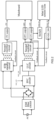
FIG.3 illustrates a structural schematic diagram on a MINI LED driving power supply provided by the present application; -
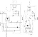
FIG.4 illustrates a circuit diagram on an enabling switching unit in the MINI LED driving power supply provided by the present application; -
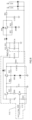
FIG.5 illustrates a circuit diagram on a standby switching subunit in the MINI LED driving power supply provided by the present application; -
FIG.6 andFIG.7 illustrate a circuit diagram on a step-down subunit in the MINI LED driving power supply provided by the present application; -
FIG.8 illustrates a circuit diagram on a power supply subunit in the MINI LED driving power supply provided by the present application; -
FIG.9 illustrates a schematic diagram on a switching sequence of the MINI LED driving power supply provided by the present application; - The present application provides a MINI LED driving power supply and a MINI LED television, being able to solve a problem of different voltages affect each other during a high power output.
- To make the objectives, technical schemes and results more explicit, further description will be made in detail to illustrate the present application. It should be understood that the specific embodiments described herein are used to explain the present application only, instead of limiting the scope of the present application.
- In addition to being used in a field of the MINI LED television, the MINI LED driving power provided by the present application can further be applied to a plurality of display-related power driving including an OLED monitor, an LED monitor, an audiovisual education, and a rear-projection plasma.
- Referring to
FIG.3 , the present application provides a MIN LED driving power supply, which comprises a power supply board connecting with amainboard 10 and aMINI LED screen 20, the power supply board comprises afirst conversion module 31 and asecond conversion module 32; thefirst conversion module 31 connects to themainboard 10 and thesecond conversion module 32, applied to outputting a power supply voltage to power themainboard 10 after thefirst conversion module 31 is powered on, and outputting a first voltage (+12V in the present embodiment) and a second voltage (+20V in the present embodiment) to power themainboard 10 according to a power-on/off signal (ON_OFF in the present embodiment) output by themainboard 10, as well as outputting a first power supply and a high-voltage direct current to thesecond conversion module 32; thesecond conversion module 32 connects to the MINI LED screen, applied to converting the high-voltage direct current into a third voltage (+28V in the present embodiment) before outputting to theMINI LED screen 20 according to an enable signal output by themainboard 10 and the first power supply, to light up theMINI LED screen 20. The present application, by converting and outputting the first voltage and the third voltage independently, and providing the third voltage to power the screen independently, makes that, whether an output of the third voltage works normally or not will not affect a working state of another line, thus a problem of an interference between a plurality of lines is avoided. - Further, the
first conversion module 31 comprises a standby control unit (not shown in the FIGs) and a first conversion unit (not shown in the drawings), the first conversion unit connects to themainboard 10, applied to outputting the power supply voltage (10V in the present embodiment) to power themainboard 10 after first conversion unit is powered on, the standby control unit connects to themainboard 10 and the first conversion unit respectively, applied to controlling the first conversion unit to start according to the power-on/off signal output by themainboard 10; the first conversion unit is further applied to outputting the first voltage and the second voltage to power themainboard 10 after the first conversion unit started, and outputting the high-voltage direct current and the first power supply to thesecond conversion module 32. Specifically, after connecting to an AC power, the power supply board outputs 10V to power themainboard 10, and themainboard 10 sends a power-on/off signal to the power supply board after working normally, making the power supply board output the first voltage to power themain board 10. After the mainboard 10 works steadily, it facilitates to control a follow-up work of thesecond conversion module 32, making thesecond conversion module 32 output the third voltage to theMINI LED screen 20, and further control theMINI LED screen 20 light up. - Further, referencing to
FIG.4 together, thesecond conversion module 32 comprises an enablingswitching unit 321 and asecond conversion unit 322; the enablingswitching unit 321 connects to the first converting unit and thesecond converting unit 322 respectively, applied to converting the first power supply (PWM_VCC in the present embodiment) into a second power supply (VCC_27V in the present embodiment) before outputting to thesecond conversion unit 322 according to the enable signal output by themainboard 10; thesecond conversion unit 322 connects to theMINI LED screen 20, applied to converting the high-voltage direct current into the third voltage to power theMINI LED screen 20 according to the second power supply, further achieving lighting up theMINI LED screen 20. In the present embodiment, the voltage outputs of thefirst conversion module 31 and thesecond conversion module 32 are independent of each other, and a voltage output of one line will not interfere with a voltage output of another line, thereby a problem of an interference between lines is avoided effectively. Due to an output of each line is separated completely, when a load of one line changes, there is no affect on an output of another line, which ensures a normal and stable operation of a system. The output voltages of the power supply board are independent, making a whole machine work stably and normally, which is able to improve an electric performance of a product, improve a picture quality experience of the MINI LED television and prolong a service life of the screen. - Further, referring to
FIG.5 ,FIG.6 , andFIG.7 together, the standby control unit comprises astandby switching subunit 311 and a step-downsubunit 312; thestandby switching subunit 311 connects to themainboard 10 and the first conversion unit respectively, applied to controlling the first conversion unit to start according to a power-on/off signal output by themainboard 10; the step-downsubunit 312 connects to themainboard 10 and the first conversion unit respectively, applied to providing a feedback signal for the first conversion unit according to the power-on/off signal. After receiving a power-on/off signal in a high level, thestandby switching subunit 311 exits a standby mode and wakes up the first conversion unit, making the first conversion unit exit the standby mode and enter a working mode. At a same time, the step-downsubunit 312 also provides a feedback signal to the first conversion unit according to the power-on/off signal in the high level, making the first conversion unit work normally and output the first voltage and the second voltage to power themainboard 10, thereby ensuring a stable operation of themainboard 10. - Further, referring to
FIG.8 , the first conversion unit comprises aconversion subunit 3121 and apower supply subunit 3122; theconversion subunit 3121 connects to thepower supply subunit 3122 and themainboard 10 respectively, applied to outputting the power supply voltage to power themainboard 10 after theconversion subunit 3121 is powered on, and outputting the first voltage and the second voltage to power themainboard 10 after theconversion subunit 3121 is started, as well as outputting the high-voltage direct current to thesecond conversion unit 322; thepower supply subunit 3122 is applied to outputting the first power supply to the enablingswitching unit 321 according to a control signal output by theconversion subunit 3121, further powering the enablingswitching unit 321, and ensuring the enablingswitching unit 321 to be able to power thesecond conversion unit 322 to work. - Further, continue referring to
FIG.3 , thesecond conversion unit 322 comprises amain LLC circuit 3221 and amain LLC transformer 3222; themain LLC circuit 3221 connects with the enablingswitching unit 321 and themain LLC transformer 3222 respectively, applied to starting themain LLC transformer 3222 according to the second power supply; themain LLC transformer 3222 connects to theMINI LED screen 20, applied to converting the high-voltage direct current into the third voltage before outputting to theMINI LED screen 20. Themain LLC circuit 3221 starts themain LLC transformer 3222 after receiving the second power supply output from the enablingswitching unit 321, then themain LLC transformer 3222 converts the high-voltage direct current before outputting the third voltage to theMINI LED screen 20, to light up theMINI LED screen 20, so as to complete a driving process of theMINI LED screen 20. - Further, the
conversion subunit 3121 comprises a bridgeless PFC circuit, an auxiliary LLC circuit, and anauxiliary LLC transformer 3211 integrated in a same semiconductor chip package, wherein a type of a chip having the bridgeless PFC circuit and an LLC controller integrated is U_MD6751, the bridgeless PFC circuit outputs a high-voltage direct current to the auxiliary LLC circuit after the bridgeless PFC circuit is started, and after the auxiliary LLC circuit controls the LLC transformer to start, theauxiliary LLC transformer 3211 converts the high-voltage direct current into the first voltage and the second voltage to supply power to themainboard 10; wherein, the bridgeless PFC circuit further outputs the high-voltage direct current to thesecond conversion module 32, so that themain LLC transformer 3222 in thesecond conversion module 32 outputs the third voltage to power theMINI LED screen 20, thus a structure of the MINI LED driving power supply in the present application adopts an independent conversion circuit, and adopts different transformers to output different voltages, thereby reducing a mutual interference between outputs. - Further, referring to
FIG.4 , the enabling switching unit 321 comprises a first diode D1, a second diode D2, a first resistor R1, a second resistor R2, a third resistor R3, a fourth resistor R4, a fifth resistor R5, a sixth resistor R6, a first triode Q1, a second triode Q2, a first capacitor C1, a second capacitor C2, a first Zener diode ZD1, and a first optocoupler OP1; an anode of the first diode D1 connects to an enable signal input terminal, an anode of the second diode D2 connects to an LED_ON signal terminal, both a cathode of the first diode D1 and a cathode of the second diode D2 connect to one end of the first resistor R1, another end of the first resistor R1, one end of the second resistor R2, and one end of the first capacitor C1 all connect to a base of the first triode Q1, an emitter of the first triode Q1, another end of the first capacitor C1, and another end of the second resistor R2 are all grounded, and a collector of the first triode Q1 connects to a second pin of the first optocoupler OP1, a first pin of the first optocoupler OP1 connects to a first voltage input terminal through the third resistor R3, a third pin of the first optocoupler OP1 connects to one end of the fourth resistor R4, another end of the fourth resistor R4 connects to one end of the fifth resistor R5, a base of the second triode Q2, and a cathode of the first Zener diode ZD1, an anode of the first Zener diode ZD1 and another end of the fifth resistor R5 are grounded, the emitter of the first triode Q1, one end of the second capacitor C2, and one end of the sixth resistor R6 are all connected to an output terminal of the second power supply, another end of the second capacitor C2 is grounded, all of a collector of the second triode Q2, a fourth pin of the first optocoupler OP1, and another end of the sixth resistor R6 connect to an input terminal of the first power supply. After themainboard 10 works stably, themainboard 10 outputs an enable signal (BL_EN in the present embodiment) to the enablingswitching unit 321, at this time, the first triode Q1 is turned on, making a conduction amount of the first optocoupler OP1 increase, a base of the second diode D2 obtains a voltage difference, before the second diode D2 is turned on in a saturation, and converting the first power supply into the second power supply to themain LLC circuit 3221, followed by themain LLC circuit 3221 starting themain LLC transformer 3222, themain LLC transformer 3222 converts the high-voltage direct current into the third voltage before supplying to theMINI LED screen 20, to light up theMINI LED screen 20. - Further, referring to
FIG.5 , thestandby switching subunit 311 comprises a third diode D3, a seventh resistor R7, an eighth resistor R8, a ninth resistor R9, a tenth resistor R10, a third triode Q3, a third capacitor C3, and a second optocoupler OP2; an anode of the third diode D3 connects to themainboard 10, a cathode of the third diode D3 connects to one end of the seventh resistor R7, all of another end of the seventh resistor R7, one end of the eighth resistor R8, and one end of the third capacitor C3 connect to a base of the third triode Q3, an emitter of the third triode Q3, another end of the third capacitor C3, and another end of the eighth resistor R8 are all grounded; a collector of the third triode Q3 connects to a second pin of the second optocoupler OP2, a first pin of the second optocoupler OP2 connects to a first voltage input terminal through the ninth resistor R9, a third pin of the second optocoupler OP2 connects to an Auto_stb signal terminal, and a fourth pin of the second optocoupler OP2 connects to a DVCC_1 signal terminal. After turning on the AC power, the power supply board outputs +10V voltage to power themainboard 10 through theconversion subunit 3121. Themainboard 10, after working normally, provides an on/off signal to the power supply board, and after thestandby switching subunit 311 receives the on/off signal, the third triode Q3 turns on in a saturation, a conduct amount of the second photocoupler OP2 increases, the DVCC_1 signal terminal powers the Auto_stb signal terminal, before waking up from a standby mode, that makes theconversion subunit 3121 exit the standby mode and enter a working state, thereby completing a loop process of the standby mode of the standby subunit. - Further, referring to
FIG.6 andFIG.7 , the step-down subunit 312 comprises a fourth diode D4, an eleventh resistor R11, a twelfth resistor R12, a fourth capacitor C4, a fourth triode Q4, a thirteenth resistor R13, a fourteenth resistor R14, a fifteenth resistor R15, a sixteenth resistor R16, a seventeenth resistor R17, an eighteenth resistor R18, a nineteenth resistor R19, a twentieth resistor R20, a twenty-first resistor R21, a twenty-second resistor R22, a twenty-third resistor R23, a fifth capacitor C5, a sixth capacitor C6, a seventh capacitor C7, an eighth capacitor C8, a ninth capacitor C9, a voltage regulator U1, a third optocoupler OP3, and a second Zener diode ZD2; an anode of the fourth diode D4 connects to the mainboard 10, a cathode of the fourth diode D4 connects to one end of the eleventh resistor R11, all of another end of the eleventh resistor R11, one end of the twelfth resistor R12, and one end of the fourth capacitor C4 connect to a base of the fourth triode Q4, an emitter of the fourth triode Q4, another end of the fourth capacitor C4, and another end of the twelfth resistor R12 are all grounded, a collector of the fourth triode Q4 connects to one end of the thirteenth resistor R13, another end of the thirteenth resistor R13 connects to one end of the fourteenth resistor R14, another end of the fourteenth resistor R14 connects to one end of the fifteenth resistor R15, one end of the seventh capacitor C7, one end of the sixth capacitor C6, one end of the fifth capacitor C5, and one end of the eighteenth resistor R18, all of one end of the seventeenth resistor R17, one end of the eighth capacitor C8, and one end of the twentieth resistor R20 connect to one end of the fifth capacitor C5, a first pin of the voltage regulator U1 connects to one end of the eighteenth resistor R18, another end of the sixth capacitor C6 connects to one end of the twenty-second resistor R22, all of another end of the twenty-second resistor R22, one end of the twenty-third resistor R23, one end of the ninth capacitor C9, another end of the seventh capacitor C7, and a second pin of the voltage regulator U1 connect to a second pin of the third photocoupler OP3, another end of the fifth capacitor C5 connects to one end of the sixteenth resistor R16, another end of the sixteenth resistor R16 and another end of the seventeenth resistor R17 are both connected to power, another end of the eighth capacitor C8 connects to one end of the nineteenth resistor R19, another end of the nineteenth resistor R19, another end of the twentieth resistor R20, and one end of the twenty-first resistor R21 are all connected to power, all of another end of the twenty-first resistor R21, one end of the twenty-third resistor 23, and a first pin of the third optocoupler OP3 connect to an OVP_1 signal terminal, another end of the fifteenth resistor R15, another end of the eighteenth resistor R18, another end of the ninth capacitor R19, and a third pin of the voltage regulator U1 are all grounded, a third pin of the third optocoupler OP3 and an anode of the second Zener diode ZD2 are both grounded, a fourth pin of the third optocoupler OP3 and a cathode of the second Zener diode ZD2 connect to an FB_2 signal terminal. Theconversion subunit 3121 enters the working state under a control of thestandby switching subunit 311, and at a same time, after receiving the on/off signal, the step-downsubunit 312 has the fourth triode Q4 saturated and turned on, the thirteenth resistor R13, the fourteenth resistor R14, and the fifteenth resistor R15 are connected in parallel, making a current flowing through the voltage regulator U1 increase, and a conduction amount of the third optocoupler OP3 increase, before the step-downsubunit 312 exits the standby mode, and at a same time a feedback signal is sent to theconversion subunit 3121, then the bridgeless PFC circuit in theconversion subunit 3121 starts to work, an output voltage of 10V becomes 12V, and theconversion subunit 3121 further outputs the first power supply and the high-voltage direct current to thesecond conversion module 32, so as to light up theMINI LED screen 20. - Further, referring to
FIG.8 , the power supply subunit 3122 comprises a fifth diode D5, a sixth diode D6, a third Zener diode ZD3, a twenty-fourth resistor R24, a twenty-fifth resistor R25, a twenty-sixth resistor R26, a twenty-seventh resistor R27, a twenty-eighth resistor R28, a twenty-ninth resistor R29, a thirtieth resistor R30, a tenth capacitor C10, an eleventh capacitor C11, a twelfth capacitor C12, a thirteenth capacitor C13, a fourteen capacitor C14, a fifth triode Q5, a sixth triode Q6, and a seventh triode Q7; another end of the twenty-fourth resistor R24 connects to a collector of the fifth triode Q5, one end of the twenty-fifth resistor R25, and one end of the tenth capacitor C10, another end of the tenth capacitor C10 and a cathode of the fifth diode D5 are grounded, an anode of the fifth diode D5 connects to an anode of the third Zener diode ZD3, all of a cathode of the third Zener diode ZD3, another end of the twenty-fifth resistor R25, and one end of the twenty-sixth resistor R26 connect to a base of the fifth triode Q5, both another end of the twenty-sixth resistor R26 and an emitter of the fifth triode Q5 connect to one end of the twenty-seventh resistor R27, one end of the eleventh capacitor C11, and an emitter of the seventh triode Q7, all of another end of the eleventh capacitor C11, an emitter of the sixth triode Q6, one end of the twenty nineteenth resistor R29, and one end of the twelfth capacitor C12 are grounded, both another end of the twenty-seventh resistor R27 and one end of the twenty-eighth resistor R28 connect to a base of the seventh triode Q7, another end of the twenty-eighth resistor R28 connects to a collector of the sixth triode Q6, all of another end of the twenty-sixth resistor R26, another end of the twelfth capacitor C12, and one end of the thirtieth resistor R30 connect to a base of the sixth triode Q6, a collector of the seventh triode Q7 and one end of the thirteenth capacitor C13 connect to an anode of the sixth diode D6, both a cathode of the sixth diode D6 and one end of the fourteenth capacitor C14 connect to an output terminal of the first power supply, another end of the fourteenth capacitor C14 gets grounded, another end of the thirteenth capacitor C13 gets grounded, another end of the thirtieth resistor R30 connects to the conversion subunit 3121 (connects to a VCC2_CTRL signal terminal in the present embodiment); after the conversion subunit 3121 starts to work, the conversion subunit 3121 controls the VCC2_CTRL signal terminal to be at a high level, turning on the sixth triode Q6 and the seventh triode Q7, further outputting the first power source to the enabling switching unit 321, to provide power for an operation of the enabling switching unit 321. - Further, a schematic diagram on a switching sequence of the MINI LED driving power supply provided by the present application is shown in
FIG.9 , further detailed description on a start-up process and a standby process of the MINI LED driving power supply provided by the present application is stated below with references toFIGs.3 to 9 : - After turning on an AC power, the power board outputs 10V to power the
mainboard 10. After working normally, an ON/OFF signal in a high-level is provided to the power board, turning on the third triode Q3, and the bridgeless PFC starts to work, boosting a voltage having been rectified to a high-voltage direct current at 400V, and outputting a VCC2_CTRL signal at a high level to control the sixth triode Q6 and the seventh triode Q7 to be turned on, a power supply sub-circuit supplies the first power supply to the enablingswitching unit 321. At a same time, when the ON/OFF signal for power switching is high, a step-down sub-circuit starts to switch to a normal working mode. After a period of about T1, the output voltage of thefirst conversion module 31 increases from 10V to 12V and 20V gradually. After a period of T2, the power supply board outputs a +12V voltage stably to supply power to themainboard 10, and after a period of T5, the 20V voltage output of the power supply board is stable. In order to light up the screen, after an interval of a period about T3, themainboard 10 sends an ENA signal at a high-level to the power board, and after receiving the ENA signal at the high-level, the enablingswitching unit 321 starts to work, converting the first power supply to the second power supply before outputting to themain LLC circuit 3221, then themain LLC circuit 3221 starts themain LLC transformer 3222 to output +28V, before theMINI LED screen 20 is lit up, and reaching a stable output after a period of T4. Thus, there is an interval of at least 36ms from starting the +12V to starting the +28V. - When the
mainboard 10 of the screen receives a standby signal, themainboard 10 outputs an ENA signal at a low level to the power board, and the enablingswitching unit 321 stops working and no longer having the second power supply output, then the power board turns off the +28V output. After another interval of a period of T6, themainboard 10 pulls the ON/OFF signal down, at this time, thestandby switching subunit 311 triggers the bridgeless PFC circuit to stop working and enter a standby state according to the ON/OFF signal at a low level, while a step-down sub-circuit provides a feedback signal according to the ON/OFF signal at the low level, making the output voltage of theconversion subunit 3121 drop from 12V to 10V to power themainboard 10, which means providing 10V for themainboard 10 during a standby; and further after a period of T7, the output voltage of 20V stops outputting, and a whole machine enters a standby state, wherein the period of T6 is no less than 30ms. - The present application, by adopting a transforming and a PFC+LLC integrated control module independently, boosts an AC input voltage to a high-voltage direct current at 400V, the high-voltage direct current is then converted into +12V and +28V independently, and by adjusting a switching sequence of a power supply according to a signal given by the
mainboard 10, the +12V and +28V are converted and output independently while controlled by the ON/OFF signal. In addition, since +28V is applied to powering the screen alone, thus another control signal ENA is arranged, and only when the ON/OFF signal and the ENA signal are both turned on at a same time, will the screen be lit up, so as to control the timing sequence of turning on/off the power to match the timing sequence of theMINI LED screen 20. Due to adopting an independent PWM controller and an independent transformer, the +12V and the +28V are independent from each other from a basis. Whether an output and a feedback adjustment circuit of each line is working normally or not, will not affect a working state of another line, thereby a problem of an interference between lines is avoided. Since an output of each line is isolated completely, there will be no effect on an output of one line when a load of another single line changes, ensuring a system work normally and stably. The voltages output from the power source board are independence, making the whole machine work stably and normally, effectively improving an electrical performance of a product, improving a picture quality experience of a MINI LED TV, and prolonging a service life of the screen. - The present application further provides a MINI LED TV correspondingly, which comprises the MINI LED driving power supply stated above. Since the MINI LED driving power supply has been described in details above, no more descriptions in details are stated herein.
- All above, the present application provides a MINI LED driving power supply and a MINI LED television, the MINI LED driving power supply comprises a power supply board connecting with a mainboard and a MINI LED screen, the power supply board comprises a first conversion module and a second conversion module; the first conversion module connects to the mainboard and the second conversion module, applied to outputting a power supply voltage to power the mainboard after the first conversion module is turned on, and outputting a first voltage and a second voltage to power the mainboard according to a power-on/off signal output by the mainboard, as well as outputting a first power supply and a high-voltage direct current to the second conversion module; the second conversion module connects to the MINI LED screen, applied to converting the high-voltage direct current into a third voltage before outputting to the MINI LED screen according to an enable signal output by the mainboard and the first power supply, to light up the MINI LED screen. By converting and outputting the first voltage and the third voltage independently, the present application makes that, whether an output of the third voltage works normally or not has no effect on a working state of another line, thus a problem of an interference between a plurality of lines is avoided.
- It should be understood that the application of the present application is not limited to the above examples and can be improved or transformed by those skilled in the art based on the above description. All these improvements and transformations should fall within the protection scope of the appended claims of the present application.
Claims (15)
- A MINI LED driving power supply, comprising a power supply board connecting with a mainboard and a MINI LED screen, wherein the power supply board comprising a first conversion module and a second conversion module;the first conversion module is connected to the mainboard and the second conversion module, configured to output a power supply voltage to power the mainboard after the first conversion module is powered on, and output a first voltage and a second voltage to power the mainboard according to a power-on/off signal output by the mainboard, as well as output a first power supply and a high-voltage direct current to the second conversion module;the second conversion module is connected to the MINI LED screen, configured to convert the high-voltage direct current into a third voltage and output the third voltage to the MINI LED screen according to an enable signal output by the mainboard and the first power supply, to light up the MINI LED screen.
- The MINI LED driving power supply as claimed in claim 1, wherein the first conversion module comprises a standby control unit and a first conversion unit;the first conversion unit is connected to the mainboard, configured to output the power supply voltage to power the mainboard after the first conversion unit is powered on;the standby control unit is connected to the mainboard and the first conversion unit, respectively, configured to control the first conversion unit to start according to the power-on/off signal output by the mainboard;the first conversion unit is further configured to output the first voltage and the second voltage to power the mainboard after the first conversion unit is started, and output the high-voltage direct current and the first power supply to the second conversion module.
- The MINI LED driving power supply as claimed in claim 2, wherein the second conversion module comprises an enabling switching unit and a second conversion unit;the enabling switching unit is connected to the first converting unit and the second converting unit, respectively, configured to convert the first power supply into a second power supply and output the second power supply to the second conversion unit according to the enable signal output by the mainboard;the second conversion unit is connected to the MINI LED screen, configured to convert the high-voltage direct current into the third voltage to power the MINI LED screen according to the second power supply.
- The MINI LED driving power supply as claimed in claim 2, wherein the standby control unit comprises a standby switching subunit and a step-down subunit;the standby switching subunit is connected to the mainboard and the first conversion unit, respectively, configured to control the first conversion unit to start according to the power-on/off signal output by the mainboard;the step-down subunit is connected to the mainboard and the first conversion unit, respectively, configured to provide a feedback signal for the first conversion unit according to the power-on/off signal.
- The MINI LED driving power supply as claimed in claim 3, wherein the first conversion unit comprises a conversion subunit and a power supply subunit;the conversion subunit is connected to the power supply subunit and the mainboard, respectively, configured to output the power supply voltage to power the mainboard after the conversion subunit is powered on, output the first voltage and the second voltage to power the mainboard after the conversion subunit is started, and output the high-voltage direct current to the second conversion unit;the power supply subunit is configured to output the first power supply to the enabling switching unit according to a control signal output by the conversion subunit.
- The MINI LED driving power supply as claimed in claim 3, wherein the second conversion unit comprises a main LLC circuit and a main LLC transformer;the main LLC circuit is connected to the enabling switching unit and the main LLC transformer, respectively, configured to start the main LLC transformer according to the second power supply;the main LLC transformer is connected to the MINI LED screen, configured to convert the high-voltage direct current into the third voltage and output the third voltage to the MINI LED screen.
- The MINI LED driving power supply as claimed in claim 3, wherein the enabling switching unit comprises a first diode, a second diode, a first resistor, a second resistor, a third resistor, a fourth resistor, a fifth resistor, a sixth resistor, a first triode, a second triode, a first capacitor, a second capacitor, a first Zener diode, and a first optocoupler;
an anode of the first diode is connected to an enable signal input terminal; an anode of the second diode is connected to an LED_ON signal terminal; both a cathode of the first diode and a cathode of the second diode are connected to one end of the first resistor; another end of the first resistor, one end of the second resistor, and one end of the first capacitor are all connected to a base of the first triode; an emitter of the first triode, another end of the first capacitor, and another end of the second resistor are all grounded; and a collector of the first triode is connected to a second pin of the first optocoupler; a first pin of the first optocoupler is connected to a first voltage input terminal through the third resistor; a third pin of the first optocoupler is connected to one end of the fourth resistor; another end of the fourth resistor is connected to one end of the fifth resistor, a base of the second triode, and a cathode of the first Zener diode; an anode of the first Zener diode and another end of the fifth resistor are grounded; the emitter of the second triode, one end of the second capacitor, and one end of the sixth resistor are all connected to an output terminal of the second power supply; another end of the second capacitor is grounded; a collector of the second triode, a fourth pin of the first optocoupler, and another end of the sixth resistor are all connected to the input terminal of the first power supply. - The MINI LED driving power supply as claimed in claim 4, wherein the standby switching subunit comprises a third diode, a seventh resistor, an eighth resistor, a ninth resistor, a tenth resistor, a third triode, a third capacitor, and a second optocoupler;
an anode of the third diode is connected to the mainboard, a cathode of the third diode is connected to one end of the seventh resistor; another end of the seventh resistor, one end of the eighth resistor, and one end of the third capacitor are all connected to a base of the third triode; an emitter of the third triode, another end of the third capacitor, and another end of the eighth resistor are all grounded; a collector of the third triode is connected to a second pin of the second optocoupler; a first pin of the second optocoupler is connected to a first voltage input terminal through the ninth resistor; a third pin of the second optocoupler is connected to an Auto_stb signal terminal; and a fourth pin of the second optocoupler is connected to a DVCC_1 signal terminal. - The MINI LED driving power supply as claimed in claim 4, wherein the step-down subunit comprises a fourth diode, an eleventh resistor, a twelfth resistor, a fourth capacitor, a fourth triode, a thirteenth resistor, a fourteenth resistor, a fifteenth resistor, a sixteenth resistor, a seventeenth resistor, an eighteenth resistor, a nineteenth resistor, a twentieth resistor, a twenty-first resistor, a twenty-second resistor, a twenty-third resistor, a fifth capacitor, a sixth capacitor, a seventh capacitor, an eighth capacitor, a ninth capacitor, a voltage regulator, a third optocoupler, and a second Zener diode;
an anode of the fourth diode is connected to the mainboard; a cathode of the fourth diode is connected to one end of the eleventh resistor; another end of the eleventh resistor, one end of the twelfth resistor, and one end of the fourth capacitor are all connected to a base of the fourth triode; an emitter of the fourth triode, another end of the fourth capacitor, and another end of the twelfth resistor are all grounded; a collector of the fourth triode is connected to one end of the thirteenth resistor; another end of the thirteenth resistor is connected to one end of the fourteenth resistor; another end of the fourteenth resistor is connected to one end of the fifteenth resistor, one end of the seventh capacitor, one end of the sixth capacitor, one end of the fifth capacitor, and one end of the eighteenth resistor; one end of the seventeenth resistor, one end of the eighth capacitor, and one end of the twentieth resistor are all connected to one end of the fifth capacitor; a first pin of the voltage regulator is connected to one end of the eighteenth resistor; another end of the sixth capacitor is connected to one end of the twenty-second resistor; another end of the twenty-second resistor, one end of the twenty-third resistor, one end of the ninth capacitor, another end of the seventh capacitor, and a second pin of the voltage regulator are all connected to a second pin of the third photocoupler; another end of the fifth capacitor is connected to one end of the sixteenth resistor; another end of the sixteenth resistor and another end of the seventeenth resistor are both grounded; another end of the eighth capacitor is connected to one end of the nineteenth resistor; another end of the nineteenth resistor, another end of the twentieth resistor, and one end of the twenty-first resistor are all connected to power; another end of the twenty-first resistor, one end of the twenty-third resistor, and a first pin of the third optocoupler are all connected to an OVP_1 signal terminal; another end of the fifteenth resistor, another end of the eighteenth resistor, another end of the ninth capacitor, and a third pin of the voltage regulator are all grounded; a third pin of the third photocoupler and an anode of the second Zener diode are both grounded; a fourth pin of the third photocoupler and a cathode of the second Zener diode are connected to an FB_2 signal terminal. - The MINI LED driving power supply as claimed in claim 5, wherein the conversion subunit comprises a bridgeless PFC circuit, an auxiliary LLC circuit, and an auxiliary LLC transformer integrated in a same semiconductor chip package, the bridgeless PFC circuit outputs a high-voltage direct current to the auxiliary LLC circuit after the bridgeless PFC circuit is started, and after the auxiliary LLC circuit controls the LLC transformer to start, the auxiliary LLC transformer converts the high-voltage direct current into the first voltage and the second voltage to supply power to the mainboard.
- The MINI LED driving power supply as claimed in claim 10, wherein the bridgeless PFC circuit further outputs the high-voltage direct current to the second conversion module, and the main LLC transformer in the second conversion module outputs the third voltage to power the MINI LED screen.
- The MINI LED driving power supply as claimed in claim 10, wherein a type of the semiconductor chip is U_MD6751.
- The MINI LED driving power supply as claimed in claim 5, wherein the power supply subunit comprises a fifth diode, a sixth diode, a third Zener diode, a twenty-fourth resistor, a twenty-fifth resistor, a twenty-sixth resistor, a twenty-seventh resistor, a twenty-eighth resistor, a twenty-ninth resistor, a thirtieth resistor, a tenth capacitor, an eleventh capacitor, a twelfth capacitor, a thirteenth capacitor, a fourteen capacitor, a fifth triode, a sixth triode, and a seventh triode;
another end of the twenty-fourth resistor is connected to a collector of the fifth triode, one end of the twenty-fifth resistor, and one end of the tenth capacitor; another end of the tenth capacitor and a cathode of the fifth diode are grounded; an anode of the fifth diode is connected to an anode of the third Zener diode; a cathode of the third Zener diode, another end of the twenty-fifth resistor, and one end of the twenty-sixth resistor are all connected to a base of the fifth triode; another end of the twenty-sixth resistor and an emitter of the fifth triode are both connected to one end of the twenty-seventh resistor, one end of the eleventh capacitor, and an emitter of the seventh triode; another end of the eleventh capacitor, an emitter of the sixth triode, one end of the twenty nineteenth resistor, and one end of the twelfth capacitor are all grounded; another end of the twenty-seventh resistor and one end of the twenty-eighth resistor are both connected to a base of the seventh triode; another end of the twenty-eighth resistor is connected to a collector of the sixth triode; another end of the twenty-sixth resistor, another end of the twelfth capacitor, and one end of the thirtieth resistor are all connected to a base of the sixth triode; a collector of the seventh triode and one end of the thirteenth capacitor are connected to an anode of the sixth diode; a cathode of the sixth diode and one end of the fourteenth capacitor are both connected to an output terminal of the first power supply; another end of the fourteenth capacitor gets grounded; another end of the thirteenth capacitor gets grounded; another end of the thirtieth resistor is connected to the conversion subunit. - The MINI LED driving power supply as claimed in claim 13, wherein the another end of the thirtieth resistor is connected to a VCC2_CTRL signal terminal, after the conversion subunit starts to work, the conversion subunit controls the VCC2_CTRL signal terminal to be at a high level, to turn on the sixth triode and the seventh triode, further outputs the first power source to the enabling switching unit, to provide power for an operation of the enabling switching unit.
- A MINI LED television, wherein comprising the MINI LED driving power supply according to any one of claims 1-14.
Applications Claiming Priority (2)
| Application Number | Priority Date | Filing Date | Title |
|---|---|---|---|
| CN202110855542.7A CN113593486B (en) | 2021-07-28 | 2021-07-28 | MINI LED drive power supply and MINI LED TV |
| PCT/CN2021/143153 WO2023005146A1 (en) | 2021-07-28 | 2021-12-30 | Mini led driving power source and mini led television |
Publications (2)
| Publication Number | Publication Date |
|---|---|
| EP4195194A1 true EP4195194A1 (en) | 2023-06-14 |
| EP4195194A4 EP4195194A4 (en) | 2023-12-27 |
Family
ID=78251173
Family Applications (1)
| Application Number | Title | Priority Date | Filing Date |
|---|---|---|---|
| EP21951718.2A Pending EP4195194A4 (en) | 2021-07-28 | 2021-12-30 | DRIVING POWER SOURCE OF MINI LED AND MNI LED TV |
Country Status (4)
| Country | Link |
|---|---|
| US (1) | US12131687B2 (en) |
| EP (1) | EP4195194A4 (en) |
| CN (1) | CN113593486B (en) |
| WO (1) | WO2023005146A1 (en) |
Families Citing this family (3)
| Publication number | Priority date | Publication date | Assignee | Title |
|---|---|---|---|---|
| CN113593486B (en) | 2021-07-28 | 2022-11-04 | 深圳创维-Rgb电子有限公司 | MINI LED drive power supply and MINI LED TV |
| CN114094799A (en) * | 2021-11-23 | 2022-02-25 | 无锡睿勤科技有限公司 | Power supply circuit and system for display screen |
| CN116092426A (en) * | 2022-12-30 | 2023-05-09 | 深圳创维-Rgb电子有限公司 | Display driving power supply, control method and device thereof |
Family Cites Families (17)
| Publication number | Priority date | Publication date | Assignee | Title |
|---|---|---|---|---|
| US8610411B2 (en) * | 2011-01-27 | 2013-12-17 | Apple Inc. | High-voltage regulated power supply |
| CN103889118B (en) * | 2014-03-18 | 2016-02-10 | 深圳创维-Rgb电子有限公司 | A kind of OLED drive electric power unit |
| CN105322803B (en) * | 2015-11-02 | 2018-03-06 | 深圳创维-Rgb电子有限公司 | Constant pressure and flow synchronism output power supply and television set |
| CN106409220B (en) | 2016-09-29 | 2019-01-29 | 深圳创维-Rgb电子有限公司 | A kind of OLED drive electric power unit and OLED TV |
| KR102579291B1 (en) * | 2018-02-07 | 2023-09-18 | 삼성전자주식회사 | Apparatus for Power Conversion and AC to DC Conversion |
| CN108521223B (en) * | 2018-04-24 | 2019-09-13 | 上海推拓科技有限公司 | Switching power circuit |
| CN109166519A (en) * | 2018-09-07 | 2019-01-08 | 深圳创维-Rgb电子有限公司 | A kind of OLED driving power and OLED TV |
| CN109119021A (en) * | 2018-09-07 | 2019-01-01 | 深圳创维-Rgb电子有限公司 | A kind of OLED driving power and OLED TV |
| CN109637461B (en) * | 2018-12-20 | 2020-07-07 | 深圳创维-Rgb电子有限公司 | A mini LED TV control system and method |
| TW202118090A (en) * | 2019-10-17 | 2021-05-01 | 徐夫子 | Resonant light-emitting module particularly related to a resonance type light emitting module involving LC resonance |
| CN110880294B (en) * | 2019-12-10 | 2021-11-09 | 深圳创维-Rgb电子有限公司 | OLED driving power supply and electronic product |
| CN111669528B (en) * | 2020-05-11 | 2022-07-01 | 深圳创维-Rgb电子有限公司 | An OLED driving power supply and OLED TV |
| CN111818284B (en) * | 2020-07-08 | 2022-11-29 | 康佳集团股份有限公司 | Regional dimming system and method for ultra-high-definition television |
| CN112350279B (en) * | 2020-09-02 | 2022-06-28 | 海信视像科技股份有限公司 | Power Protection Circuits and Electronic Equipment |
| CN112349249B (en) * | 2020-11-03 | 2021-12-28 | 深圳创维-Rgb电子有限公司 | An OLED driving power supply and OLED TV |
| CN113035138A (en) * | 2021-03-09 | 2021-06-25 | 京东方科技集团股份有限公司 | Driving circuit, display screen and driving method |
| CN113593486B (en) * | 2021-07-28 | 2022-11-04 | 深圳创维-Rgb电子有限公司 | MINI LED drive power supply and MINI LED TV |
-
2021
- 2021-07-28 CN CN202110855542.7A patent/CN113593486B/en active Active
- 2021-12-30 EP EP21951718.2A patent/EP4195194A4/en active Pending
- 2021-12-30 US US18/044,447 patent/US12131687B2/en active Active
- 2021-12-30 WO PCT/CN2021/143153 patent/WO2023005146A1/en not_active Ceased
Also Published As
| Publication number | Publication date |
|---|---|
| US12131687B2 (en) | 2024-10-29 |
| EP4195194A4 (en) | 2023-12-27 |
| CN113593486B (en) | 2022-11-04 |
| CN113593486A (en) | 2021-11-02 |
| US20230343273A1 (en) | 2023-10-26 |
| WO2023005146A1 (en) | 2023-02-02 |
Similar Documents
| Publication | Publication Date | Title |
|---|---|---|
| US11115618B2 (en) | Television power supply driving device and television | |
| US11308871B2 (en) | OLED drive power supply and OLED television | |
| US10694138B2 (en) | OLED drive power device and OLED television | |
| CN106488607B (en) | Switching Power Supply and television set | |
| US12230225B2 (en) | Display apparatus and display control method | |
| US12131687B2 (en) | Mini LED driving power supply and mini LED television | |
| CN108231014B (en) | Regional dimming constant current control circuit, driving power supply and television | |
| EP3848921B1 (en) | Oled driving power source and oled television | |
| CN111669528B (en) | An OLED driving power supply and OLED TV | |
| US11825577B2 (en) | Display apparatus and step power circuit | |
| CN110769173B (en) | Television power supply system and television | |
| CN111371094B (en) | A dual power supply system and a TV | |
| EP1879383A2 (en) | Power supply circuit for a liquid crystal display device | |
| CN223639175U (en) | Switching power supply circuit and dimming device applying same | |
| CN224191838U (en) | A power-on timing control circuit | |
| CN223207003U (en) | Power supply circuit of miniLED TV | |
| CN215897587U (en) | Display device | |
| CN120726931A (en) | An energy efficiency control circuit and PD product combining single-stage PFC and TFT screen | |
| KR19990003849A (en) | Monitor power circuit | |
| KR100287846B1 (en) | Apparatus for Reducing DPM Mode Consumption Power of Monitor | |
| JP2001258255A (en) | Switching power supply | |
| JP2011029042A (en) | Electrical circuit for driving cold light backlight panel |
Legal Events
| Date | Code | Title | Description |
|---|---|---|---|
| STAA | Information on the status of an ep patent application or granted ep patent |
Free format text: STATUS: THE INTERNATIONAL PUBLICATION HAS BEEN MADE |
|
| PUAI | Public reference made under article 153(3) epc to a published international application that has entered the european phase |
Free format text: ORIGINAL CODE: 0009012 |
|
| STAA | Information on the status of an ep patent application or granted ep patent |
Free format text: STATUS: REQUEST FOR EXAMINATION WAS MADE |
|
| 17P | Request for examination filed |
Effective date: 20230308 |
|
| AK | Designated contracting states |
Kind code of ref document: A1 Designated state(s): AL AT BE BG CH CY CZ DE DK EE ES FI FR GB GR HR HU IE IS IT LI LT LU LV MC MK MT NL NO PL PT RO RS SE SI SK SM TR |
|
| RIC1 | Information provided on ipc code assigned before grant |
Ipc: G09G 3/34 20060101AFI20230908BHEP |
|
| A4 | Supplementary search report drawn up and despatched |
Effective date: 20231123 |
|
| RIC1 | Information provided on ipc code assigned before grant |
Ipc: G09G 3/34 20060101AFI20231117BHEP |
|
| DAV | Request for validation of the european patent (deleted) | ||
| DAX | Request for extension of the european patent (deleted) | ||
| STAA | Information on the status of an ep patent application or granted ep patent |
Free format text: STATUS: EXAMINATION IS IN PROGRESS |
|
| 17Q | First examination report despatched |
Effective date: 20251217 |