EP4194817A1 - Ratiometric position measurement - Google Patents
Ratiometric position measurement Download PDFInfo
- Publication number
- EP4194817A1 EP4194817A1 EP22208581.3A EP22208581A EP4194817A1 EP 4194817 A1 EP4194817 A1 EP 4194817A1 EP 22208581 A EP22208581 A EP 22208581A EP 4194817 A1 EP4194817 A1 EP 4194817A1
- Authority
- EP
- European Patent Office
- Prior art keywords
- signal
- bit
- signal path
- multiplexer
- sensor
- Prior art date
- Legal status (The legal status is an assumption and is not a legal conclusion. Google has not performed a legal analysis and makes no representation as to the accuracy of the status listed.)
- Granted
Links
Images



Classifications
-
- G—PHYSICS
- G01—MEASURING; TESTING
- G01D—MEASURING NOT SPECIALLY ADAPTED FOR A SPECIFIC VARIABLE; ARRANGEMENTS FOR MEASURING TWO OR MORE VARIABLES NOT COVERED IN A SINGLE OTHER SUBCLASS; TARIFF METERING APPARATUS; MEASURING OR TESTING NOT OTHERWISE PROVIDED FOR
- G01D5/00—Mechanical means for transferring the output of a sensing member; Means for converting the output of a sensing member to another variable where the form or nature of the sensing member does not constrain the means for converting; Transducers not specially adapted for a specific variable
- G01D5/12—Mechanical means for transferring the output of a sensing member; Means for converting the output of a sensing member to another variable where the form or nature of the sensing member does not constrain the means for converting; Transducers not specially adapted for a specific variable using electric or magnetic means
- G01D5/14—Mechanical means for transferring the output of a sensing member; Means for converting the output of a sensing member to another variable where the form or nature of the sensing member does not constrain the means for converting; Transducers not specially adapted for a specific variable using electric or magnetic means influencing the magnitude of a current or voltage
- G01D5/20—Mechanical means for transferring the output of a sensing member; Means for converting the output of a sensing member to another variable where the form or nature of the sensing member does not constrain the means for converting; Transducers not specially adapted for a specific variable using electric or magnetic means influencing the magnitude of a current or voltage by varying inductance, e.g. by a movable armature
-
- G—PHYSICS
- G01—MEASURING; TESTING
- G01D—MEASURING NOT SPECIALLY ADAPTED FOR A SPECIFIC VARIABLE; ARRANGEMENTS FOR MEASURING TWO OR MORE VARIABLES NOT COVERED IN A SINGLE OTHER SUBCLASS; TARIFF METERING APPARATUS; MEASURING OR TESTING NOT OTHERWISE PROVIDED FOR
- G01D5/00—Mechanical means for transferring the output of a sensing member; Means for converting the output of a sensing member to another variable where the form or nature of the sensing member does not constrain the means for converting; Transducers not specially adapted for a specific variable
- G01D5/12—Mechanical means for transferring the output of a sensing member; Means for converting the output of a sensing member to another variable where the form or nature of the sensing member does not constrain the means for converting; Transducers not specially adapted for a specific variable using electric or magnetic means
- G01D5/14—Mechanical means for transferring the output of a sensing member; Means for converting the output of a sensing member to another variable where the form or nature of the sensing member does not constrain the means for converting; Transducers not specially adapted for a specific variable using electric or magnetic means influencing the magnitude of a current or voltage
-
- G—PHYSICS
- G01—MEASURING; TESTING
- G01D—MEASURING NOT SPECIALLY ADAPTED FOR A SPECIFIC VARIABLE; ARRANGEMENTS FOR MEASURING TWO OR MORE VARIABLES NOT COVERED IN A SINGLE OTHER SUBCLASS; TARIFF METERING APPARATUS; MEASURING OR TESTING NOT OTHERWISE PROVIDED FOR
- G01D5/00—Mechanical means for transferring the output of a sensing member; Means for converting the output of a sensing member to another variable where the form or nature of the sensing member does not constrain the means for converting; Transducers not specially adapted for a specific variable
- G01D5/12—Mechanical means for transferring the output of a sensing member; Means for converting the output of a sensing member to another variable where the form or nature of the sensing member does not constrain the means for converting; Transducers not specially adapted for a specific variable using electric or magnetic means
- G01D5/14—Mechanical means for transferring the output of a sensing member; Means for converting the output of a sensing member to another variable where the form or nature of the sensing member does not constrain the means for converting; Transducers not specially adapted for a specific variable using electric or magnetic means influencing the magnitude of a current or voltage
- G01D5/20—Mechanical means for transferring the output of a sensing member; Means for converting the output of a sensing member to another variable where the form or nature of the sensing member does not constrain the means for converting; Transducers not specially adapted for a specific variable using electric or magnetic means influencing the magnitude of a current or voltage by varying inductance, e.g. by a movable armature
- G01D5/22—Mechanical means for transferring the output of a sensing member; Means for converting the output of a sensing member to another variable where the form or nature of the sensing member does not constrain the means for converting; Transducers not specially adapted for a specific variable using electric or magnetic means influencing the magnitude of a current or voltage by varying inductance, e.g. by a movable armature differentially influencing two coils
- G01D5/2291—Linear or rotary variable differential transformers (LVDTs/RVDTs) having a single primary coil and two secondary coils
-
- G—PHYSICS
- G01—MEASURING; TESTING
- G01D—MEASURING NOT SPECIALLY ADAPTED FOR A SPECIFIC VARIABLE; ARRANGEMENTS FOR MEASURING TWO OR MORE VARIABLES NOT COVERED IN A SINGLE OTHER SUBCLASS; TARIFF METERING APPARATUS; MEASURING OR TESTING NOT OTHERWISE PROVIDED FOR
- G01D5/00—Mechanical means for transferring the output of a sensing member; Means for converting the output of a sensing member to another variable where the form or nature of the sensing member does not constrain the means for converting; Transducers not specially adapted for a specific variable
- G01D5/12—Mechanical means for transferring the output of a sensing member; Means for converting the output of a sensing member to another variable where the form or nature of the sensing member does not constrain the means for converting; Transducers not specially adapted for a specific variable using electric or magnetic means
- G01D5/244—Mechanical means for transferring the output of a sensing member; Means for converting the output of a sensing member to another variable where the form or nature of the sensing member does not constrain the means for converting; Transducers not specially adapted for a specific variable using electric or magnetic means influencing characteristics of pulses or pulse trains; generating pulses or pulse trains
- G01D5/24471—Error correction
- G01D5/2448—Correction of gain, threshold, offset or phase control
-
- H—ELECTRICITY
- H03—ELECTRONIC CIRCUITRY
- H03M—CODING; DECODING; CODE CONVERSION IN GENERAL
- H03M1/00—Analogue/digital conversion; Digital/analogue conversion
- H03M1/12—Analogue/digital converters
-
- H—ELECTRICITY
- H04—ELECTRIC COMMUNICATION TECHNIQUE
- H04L—TRANSMISSION OF DIGITAL INFORMATION, e.g. TELEGRAPHIC COMMUNICATION
- H04L67/00—Network arrangements or protocols for supporting network services or applications
- H04L67/01—Protocols
- H04L67/12—Protocols specially adapted for proprietary or special-purpose networking environments, e.g. medical networks, sensor networks, networks in vehicles or remote metering networks
Definitions
- the present invention generally relates to sensor position measurements, and more specifically, to an improved topology for alternating current (AC) ratiometric position measurements
- Resolvers and linear variable differential transformers are used in a variety of applications to provide position feedback.
- resolvers are oftentimes associated with actuators to provide feedback regarding the state of the actuator (e.g., open, partially open, closed) LVDTs and resolvers each generate a pair of alternating current (AC) sensor signals that together indicate position and/or angle.
- AC alternating current
- a resolver and/or LVDT monitors the excitation signal and the corresponding output signals simultaneously to determine position.
- a multiplexer is used to sample the respective signals successively as opposed to simultaneously. Monitoring the sampled signals successively requires additional circuitry referred to as a signal conditioning circuit. Design of these signal conditioning circuits must weigh the cost of the individual components against the sampling speed for each signal while serving multiple sensors aboard an aircraft.
- Embodiments of the present invention are directed to a system.
- a nonlimiting example of the system includes a signal conditioning circuit including a first signal path comprising a first multiplexer connected to a first filter, wherein the first signal path receives a first secondary signal from a first sensor and a built in test (BIT) signal, a second signal path comprising a second multiplexer connected to a second filter, wherein the second signal path receives a second secondary signal from the first sensor and the BIT signal, wherein the first signal path and the second signal path are connected to a third multiplexer, and a first analog to digital converter (ADC) connected to an output of the third multiplexer, and a controller connected to an output of the first ADC, wherein the controller is configured to determine a position measurement for the first sensor based on the first secondary signal, the second secondary signal, and the BIT signal.
- ADC analog to digital converter
- the signal conditioning circuit further includes a third signal path comprising a fourth multiplexer connected to a third filter, wherein the third signal path receives a third secondary signal from a second sensor and the BIT signal, a fourth signal path comprising a fifth multiplexer connected to a fourth filter, wherein the fourth signal path receives a fourth secondary signal from the second sensor and the BIT signal, wherein the third signal path and the fourth signal path are connected to a sixth multiplexer, a second ADC connected to an output of the sixth multiplexer, wherein the controller is connected to an output of the second ADC and wherein the controller is further configured to determine a position measurement of the second sensor based on the third secondary signal, the fourth secondary signal, and the BIT signal.
- further embodiments of the system may include that the first signal path further receives an excitation signal into an input of the first multiplexer.
- further embodiments of the system may include that the BIT signal comprises a square wave having a first frequency.
- excitation signal comprises a second frequency; and wherein the first frequency is equivalent to the first frequency.
- further embodiments of the system may include that the first sensor comprises a linear variable differential transformer.
- further embodiments of the system may include that the first sensor comprises a resolver.
- further embodiments of the system may include that the first filter comprises a 2-pole filter.
- controller comprises a field programmable gate array (FPGA).
- FPGA field programmable gate array
- Embodiments of the present invention are directed to a method.
- a nonlimiting example of the method includes receiving, through a first signal path, a first secondary signal from a first sensor and a built in test (BIT) signal, wherein the first signal path comprises a first multiplexer connected to a first filter, receiving, through a second signal path, a second secondary signal from the first sensor and the BIT signal, wherein the second signal path comprises a second multiplexer connected to a second filter, wherein the first signal path and the second signal path are connected to a third multiplexer, wherein the third multiplexer is connected to a first analog to digital converter (ADC), receiving, by a controller, an output signal from an output of the first ADC, and determining, by the controller, a position measurement for the first sensor based on the first secondary signal, the second secondary signal, and the BIT signal.
- ADC analog to digital converter
- further embodiments of the method may include receiving, through a third signal path, a third secondary signal from a second sensor and the BIT signal, wherein the third signal path comprises a fourth multiplexer connected to a third filter, receiving, through a fourth signal path, a fourth secondary signal from the second sensor and the BIT signal, wherein the fourth signal path comprises a fifth multiplexer connected to a third filter, wherein the third signal path and the fourth signal path are connected to a sixth multiplexer, wherein the sixth multiplexer is connected to a second analog to digital converter (ADC), receiving, by the controller, an output signal from an output of the second ADC, and determining, by the controller, a position measurement for the second sensor based on the third secondary signal, the fourth secondary signal, and the BIT signal.
- ADC analog to digital converter
- further embodiments of the method may include that the first signal path further receives an excitation signal into an input of the first multiplexer.
- further embodiments of the method may include that the BIT signal comprises a square wave having a first frequency.
- excitation signal comprises a second frequency; and wherein the first frequency is equivalent to the first frequency.
- further embodiments of the method may include that the first sensor comprises a linear variable differential transformer.
- further embodiments of the method may include that the first sensor comprises a resolver.
- further embodiments of the method may include that the first filter comprises a 2-pole filter.
- controller comprises a field programmable gate array (FPGA).
- FPGA field programmable gate array
- FIG. 1 illustrates an example of a commercial aircraft 10 having aircraft engines 20 that may embody aspects of the teachings of this disclosure.
- the aircraft 10 includes two wings 22 that each include one or more slats 24 and one or more flaps 26.
- the aircraft further includes ailerons 27, spoilers 28, horizontal stabilizer trim tabs 29, rudder 30 and horizontal stabilizer 31.
- the term "control surface" used herein includes but is not limited to either a slat or a flap or any of the above described. It will be understood that the slats 24 and/or the flaps 26 can include one or more slat/flap panels that move together.
- the example aircraft 10 includes an actuator 18. Connected to the actuator 18 is a transformer based sensor 32.
- the senor 32 is a linear variable differential transformer, a rotary variable differential transformer, or a resolver.
- the transformer based sensor 32 is connected to a processing system 50, such as an aircraft controller, via two sensor cables 40, 42.
- the processing system 50 determines the position of the actuator based on the relative amplitudes of the two sensor cables 40, 42, and utilizes the determined information to control the actuator 18.
- FIG. 2 depicts an example linear variable differential transformer.
- the example linear variable differential transformer sensor 100 that can be used as the transformer based sensor 32 of FIG. 1 .
- the linear variable differential transformer sensor 100 includes an input winding 110 connected to an AC excitation voltage source 112. Across from the input winding 110 are two output windings 120, 130 each having a corresponding output E1, E2 (sometimes referred to as "secondary outputs"). Between the output windings 120, 130 is a sliding magnetic core 140.
- the sliding magnetic core 140 is connected to an actuator and slides as the actuator moves. The shifting of the magnetic core alters the number of turns connecting each output winding 120, 130 to the input winding 110, and affects a corresponding change in the current signal output on each of the outputs E1, E2.
- the core 140 remains stationary and the input winding 110 or the two output windings 120, 130 shift along with the actuator.
- FIG. 3 depicts a block diagram of an example signal conditioning circuit.
- the circuit 200 is configured to receive a plurality of alternating current (AC) input signals (VDT1_E1, VDT1_E2, VDT2_E1, VDT2 E2, other inputs) from a plurality of sensors.
- Example sensors include LVDTs, RVDTs, resolvers, and/or other sensors.
- the circuit 200 includes a first stage multiplexer (MUX) 202 which receives a total of six (6) AC input signals.
- MUX first stage multiplexer
- the AC input signals include two secondary signals from a first sensor VDT1 (VDT1 E1, VDT1 E2,), two secondary signals from a second sensor VDT2 (VDT2 E1, VDT2_E2), the shared excitation signal (VDT EXC), and a built in test (BIT) signal (VDT_BIT).
- VDT1 E1, VDT1 E2 the shared excitation signal
- VDT_BIT the built in test signal
- These signals are fed through the same signal path through the first stage multiplexer 202 and through shared antialiasing filters 204, 206 into a second stage MUX 208.
- This circuit 200 utilizes the same signal path so that any gain and/or frequency response variations caused by the first tier MUX 202 and filters 204, 206 would occur identically on the signals, and therefor the effects would cancel.
- the second tier MUX 208 selects its inputs form the outputs of the first tier MUX 202.
- the output of the second tier MUX 208 is fed into an analog to digital converter (ADC) to digitize.
- ADC analog to digital converter
- the output of the ADC 210 can be provided to controller 212 which could be a gate array, general purpose processor, and the like.
- the controller 212 determines a position measurement from the plurality of sensors.
- the position of an LVDT (the position of the core 140 - and thus the actuator) is given by the secondary windings using equation [1] below.
- the core position is given by the secondary windings using equation [2] below where the secondary windings are orthogonal. In both cases, the position is related to the ratio of the two secondary windings signals (E1, E2).
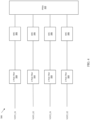
- FIG. 4 depicts a block diagram of an exemplary non-interleaved signal conditioning.
- the secondary winding signals VDT1 E1, VDT1_E2, VDT2 E1, VDT2 E2 have their own signal paths through separate filters 304 before being fed into the input of an ADC 306 and outputted to an FPGA 320 (controller). While this topology provides faster acquisition of the secondary winding signals, since the E1 and E2 signals use different filtering 304 and ADC 306 paths, any filter and/or ADC gain errors are not cancelled out here. Further, this topology requires multiple filters and multiple ADCs for proper operation. ADCs, in generally, have a higher monetary cost than multiplexers.
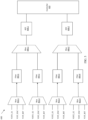
- FIG. 5 depicts a block diagram of an improved signal conditioning circuit according to one or more embodiments.
- the circuit 400 includes a plurality of signal paths for receiving an AC input signal from a sensor such as, for example, an LVDT, RVDT, and/or resolver.
- Each signal path includes a first stage MUX 402-1, 402-2, 402-3, 402-4 and a filter 404-1, 404-2, 404-3, 404-4.
- the signal paths each receive as inputs a secondary winding signal from a sensor (E1 or E2), the sensor excitation signal (VDT_EXC), and a built in test (BIT) signal (VDT_BIT).
- E1 or E2 the sensor excitation signal
- BIT built in test
- the BIT signal is utilized to verify the proper performance of the antialiasing filters 404-1, 404-2, 404-3, 404-4.
- the BIT signal is a square wave at the excitation frequency.
- the circuit 400 also includes two second stage MUXs 406-1, 406-2 that each receive two signal path inputs.
- the two signal path inputs correspond to first secondary windings E1 and second secondary windings E2 of the same VDT sensor.
- the excitation signal and the BIT signal are shared by the two sensors (VDT1 ,VDT2) and are inputs to all four first stage MUXs 402.
- the second stage MUXs 406 output to corresponding ADCs 408-1, 408-2 which digitize the signal and feed to the controller 410.
- the controller 410 can be a field programmable gate array (FPGA), a general purpose processor, and/or the like.
- FPGA field programmable gate array
- the BIT input is a square wave with an equivalent frequency of the excitation signal (VDT_EXC) and is processed with synchronous demodulation at the fundamental and third harmonic for all signal paths.
- the calculation of the position of the sensor is based on the secondary windings signals (E1, E2) and the BIT signal and is illustrated below in equation [3].
- Position E 1 / BIT 1 _ E 1 ⁇ E 2 / BIT 1 _ E 2 / E 1 / BIT 1 _ E 1 + E 2 / BIT 1 _ E 2
- BIT 1_E1 is the BIT signal selected along the E1 signal path, and processed at the fundamental frequency. This cancels any gain errors of the E1 signal path.
- BIT 1_E2 is the BIT signal selected along the E2 signal path, and processed at the fundamental frequency. This also cancels any gain errors of the E2 signal path.
- E1 refers to the first secondary winding of a sensor (e.g., LVDT) and E2 refers to the second secondary winding of the same sensor.
- Resolver Compensated Position ArcTAN E 1 / BIT 1 _ E 1 / E 2 / BIT 1 _ E 2
- Equations [3] and [4] can be referred to as a compensated position measurement equations.
- the BIT signal is used for compensation because it is entirely internal to the electronics whereas the excitation is generated by the electronics but is exposed to external influences at the sensor along the way.
- the BIT and excitation signals are steady-state and may be acquired at a lower-rate allowing the multiplexers to be wider allowing for additional signal inputs, in one or more embodiments.
- using a continual demodulation signal allows measurement of phase delay from the Excitation output to the Secondary signal inputs, which may be used for resolver quadrant information, and/or coil health.
- the illustrated examples shown in the figures has two sensors with three inputs to the first stage multiplexers, any number of sensor secondary signals can be obtained using wider multiplexers, for example.
- the sensors for a controller are acquired at the highest rate.
- the multiplexers are selected independently based on the rate of acquisition for the application. For example, one multiplexer may be skewed by one half of an acquisition cycle which would thus provide inputs to the controller at twice the rate of another multiplexer in a different signal path.
- the improved signal conditioning circuit reduces the number of ADCs required for processing sensor inputs.
- ADCs have a higher monetary cost than multiplexers.
- the monetary costs are taken into consideration with respect to the performance requirements.
- the second stage MUXs 406-1, 406-2 can be further reduced to a single second stage MUX with a single ADC outputting to the controller 410.
- the second stage MUX would be a four (4) input MUX and the total ADCs would reduce from 2 to 1.
- a second filter would be needed along the signal paths for a total of four extract filters. While this further decreases the total cost, the per signal sampling rate is also reduced.
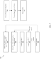
- FIG. 6 depicts a flow diagram of a method for sensor position measurements according to one or more embodiments.
- the method 600 includes receiving, through a first signal path, a first secondary signal from a first sensor and a built in test (BIT) signal, wherein the first signal path comprises a first multiplexer connected to a first filter, as shown at block 602.
- the method 600 includes receiving, through a second signal path, a second secondary signal from the first sensor and the BIT signal, wherein the second signal path comprises a second multiplexer connected to a second filter, wherein the first signal path and the second signal path are connected to a third multiplexer, wherein the third multiplexer is connected to a first analog to digital converter (ADC).
- ADC analog to digital converter
- the method 600 includes receiving, by a controller, an output signal from an output of the first ADC. And at block 608, the method 600 includes determining, by the controller, a position measurement for the first sensor based on the first secondary signal, the second secondary signal, and the BIT signals.
- FIG. 7 depicts a flow diagram of a method for sensor position measurements according to one or more embodiments.
- Each input to the multiplexers 402-1 and 402-2 (from FIG. 5 ) are to be acquired and processed without interruption to avoid disrupting the filters.
- the sequence Input, Excitation, Input, BIT allows the Input to be updated at twice the rate of the Excitation and BIT values, since the excitation and BIT values are not expected to change, except for failures and temperature variations.
- the Multiplexer 406-1 After each input is selected, for a period of the Filter settling time plus once cycle of the excitation, the Multiplexer 406-1 alternatively selects the signal through Filter 404-1 as shown in block 706, then the signal through Filter 404-2 as shown in block 707, which are each acquired by the ADV 408-1.
- the sampling rate is typically an integer multiple of the excitation frequency to reduce jitter due to aliasing of the excitation and sampling frequencies.
- the Processing element calculates the two magnitudes from the sample sets, one from the 404-1 path and one from the 404-2 path as shown in block 710. If the sample sets represent the inputs, the magnitudes are used to calculate the sensor position as shown in block 711 and outputted as shown in block 712.
Landscapes
- Physics & Mathematics (AREA)
- General Physics & Mathematics (AREA)
- Engineering & Computer Science (AREA)
- Power Engineering (AREA)
- Transmission And Conversion Of Sensor Element Output (AREA)
Abstract
Description
- The present invention generally relates to sensor position measurements, and more specifically, to an improved topology for alternating current (AC) ratiometric position measurements
- Resolvers and linear variable differential transformers (LVDTs) are used in a variety of applications to provide position feedback. For example, resolvers are oftentimes associated with actuators to provide feedback regarding the state of the actuator (e.g., open, partially open, closed) LVDTs and resolvers each generate a pair of alternating current (AC) sensor signals that together indicate position and/or angle.
- Typically, a resolver and/or LVDT monitors the excitation signal and the corresponding output signals simultaneously to determine position. However, in some applications, a multiplexer is used to sample the respective signals successively as opposed to simultaneously. Monitoring the sampled signals successively requires additional circuitry referred to as a signal conditioning circuit. Design of these signal conditioning circuits must weigh the cost of the individual components against the sampling speed for each signal while serving multiple sensors aboard an aircraft.
- Embodiments of the present invention are directed to a system. A nonlimiting example of the system includes a signal conditioning circuit including a first signal path comprising a first multiplexer connected to a first filter, wherein the first signal path receives a first secondary signal from a first sensor and a built in test (BIT) signal, a second signal path comprising a second multiplexer connected to a second filter, wherein the second signal path receives a second secondary signal from the first sensor and the BIT signal, wherein the first signal path and the second signal path are connected to a third multiplexer, and a first analog to digital converter (ADC) connected to an output of the third multiplexer, and a controller connected to an output of the first ADC, wherein the controller is configured to determine a position measurement for the first sensor based on the first secondary signal, the second secondary signal, and the BIT signal.
- In addition to one or more of the features described above, or as an alternative, further embodiments of the system may include that the signal conditioning circuit further includes a third signal path comprising a fourth multiplexer connected to a third filter, wherein the third signal path receives a third secondary signal from a second sensor and the BIT signal, a fourth signal path comprising a fifth multiplexer connected to a fourth filter, wherein the fourth signal path receives a fourth secondary signal from the second sensor and the BIT signal, wherein the third signal path and the fourth signal path are connected to a sixth multiplexer, a second ADC connected to an output of the sixth multiplexer, wherein the controller is connected to an output of the second ADC and wherein the controller is further configured to determine a position measurement of the second sensor based on the third secondary signal, the fourth secondary signal, and the BIT signal.
- In addition to one or more of the features described above, or as an alternative, further embodiments of the system may include that determining the position measurement for the first sensor based on the first secondary signal, the second secondary signal, and the built in test signal comprises calculating the position, whereby Position = (E1/BIT1_E1 - E2/BIT1_E2) / (E1/BIT1_E1 + E2/BIT1_E2), wherein E1 comprises the first secondary signal, wherein E2 comprises the second secondary signal, wherein BIT1_E1 comprises the built in test signal traversing the first signal path, and wherein BIT1_E2 comprises the built in test signal traversing the second signal path.
- In addition to one or more of the features described above, or as an alternative, further embodiments of the system may include that the first signal path further receives an excitation signal into an input of the first multiplexer.
- In addition to one or more of the features described above, or as an alternative, further embodiments of the system may include that the BIT signal comprises a square wave having a first frequency.
- In addition to one or more of the features described above, or as an alternative, further embodiments of the system may include that excitation signal comprises a second frequency; and wherein the first frequency is equivalent to the first frequency.
- In addition to one or more of the features described above, or as an alternative, further embodiments of the system may include that the first sensor comprises a linear variable differential transformer.
- In addition to one or more of the features described above, or as an alternative, further embodiments of the system may include that the first sensor comprises a resolver.
- In addition to one or more of the features described above, or as an alternative, further embodiments of the system may include that the first filter comprises a 2-pole filter.
- In addition to one or more of the features described above, or as an alternative, further embodiments of the system may include that the controller comprises a field programmable gate array (FPGA).
- Embodiments of the present invention are directed to a method. A nonlimiting example of the method includes receiving, through a first signal path, a first secondary signal from a first sensor and a built in test (BIT) signal, wherein the first signal path comprises a first multiplexer connected to a first filter, receiving, through a second signal path, a second secondary signal from the first sensor and the BIT signal, wherein the second signal path comprises a second multiplexer connected to a second filter, wherein the first signal path and the second signal path are connected to a third multiplexer, wherein the third multiplexer is connected to a first analog to digital converter (ADC), receiving, by a controller, an output signal from an output of the first ADC, and determining, by the controller, a position measurement for the first sensor based on the first secondary signal, the second secondary signal, and the BIT signal.
- In addition to one or more of the features described above, or as an alternative, further embodiments of the method may include receiving, through a third signal path, a third secondary signal from a second sensor and the BIT signal, wherein the third signal path comprises a fourth multiplexer connected to a third filter, receiving, through a fourth signal path, a fourth secondary signal from the second sensor and the BIT signal, wherein the fourth signal path comprises a fifth multiplexer connected to a third filter, wherein the third signal path and the fourth signal path are connected to a sixth multiplexer, wherein the sixth multiplexer is connected to a second analog to digital converter (ADC), receiving, by the controller, an output signal from an output of the second ADC, and determining, by the controller, a position measurement for the second sensor based on the third secondary signal, the fourth secondary signal, and the BIT signal.
- In addition to one or more of the features described above, or as an alternative, further embodiments of the method may include that determining the position measurement for the first sensor based on the first secondary signal, the second secondary signal, and the built in test signal comprises calculating the position, whereby Position = (E1/BIT1_E1 - E2/BIT1_E2) / (E1/BIT1_E1 + E2/BIT1_E2), wherein E1 comprises the first secondary signal, wherein E2 comprises the second secondary signal, wherein BIT1_E1 comprises the built in test signal traversing the first signal path, and wherein BIT1_E2 comprises the built in test signal traversing the second signal path.
- In addition to one or more of the features described above, or as an alternative, further embodiments of the method may include that the first signal path further receives an excitation signal into an input of the first multiplexer.
- In addition to one or more of the features described above, or as an alternative, further embodiments of the method may include that the BIT signal comprises a square wave having a first frequency.
- In addition to one or more of the features described above, or as an alternative, further embodiments of the method may include that excitation signal comprises a second frequency; and wherein the first frequency is equivalent to the first frequency.
- In addition to one or more of the features described above, or as an alternative, further embodiments of the method may include that the first sensor comprises a linear variable differential transformer.
- In addition to one or more of the features described above, or as an alternative, further embodiments of the method may include that the first sensor comprises a resolver.
- In addition to one or more of the features described above, or as an alternative, further embodiments of the method may include that the first filter comprises a 2-pole filter.
- In addition to one or more of the features described above, or as an alternative, further embodiments of the method may include that the controller comprises a field programmable gate array (FPGA).
- Additional technical features and benefits are realized through the techniques of the present invention. Embodiments and aspects of the invention are described in detail herein and are considered a part of the claimed subject matter. For a better understanding, refer to the detailed description and to the drawings.
- The specifics of the exclusive rights described herein are particularly pointed out and distinctly claimed in the claims at the conclusion of the specification. The foregoing and other features and advantages of the embodiments of the invention are apparent from the following detailed description taken in conjunction with the accompanying drawings in which:
-
FIG. 1 is a perspective view of an aircraft that may incorporate embodiments of the present disclosure; -
FIG. 2 depicts an example linear variable differential transformer; -
FIG. 3 depicts a block diagram of an example signal conditioning circuit; -
FIG. 4 depicts a block diagram of an exemplary non-interleaved signal conditioning; -
FIG. 5 depicts a block diagram of an improved signal conditioning circuit according to one or more embodiments; -
FIG. 6 depicts a flow diagram of a method for sensor position measurements according to one or more embodiments; and -
FIG. 7 depicts a flow diagram of a method for sensor position measurements according to one or more embodiments. - The diagrams depicted herein are illustrative. There can be many variations to the diagram or the operations described therein without departing from the spirit of the invention. For instance, the actions can be performed in a differing order or actions can be added, deleted or modified. Also, the term "coupled" and variations thereof describes having a communications path between two elements and does not require but does include a direct connection between the elements with no intervening elements/connections between them. All of these variations are considered a part of the specification.
- For the sake of brevity, conventional techniques related to making and using aspects of the invention may or may not be described in detail herein. In particular, various aspects of aircraft electric power systems to implement the various technical features described herein are well known. Accordingly, many conventional implementation details are only mentioned briefly herein or are omitted entirely without providing the well-known system and/or process details.
-
FIG. 1 illustrates an example of acommercial aircraft 10 havingaircraft engines 20 that may embody aspects of the teachings of this disclosure. Theaircraft 10 includes twowings 22 that each include one ormore slats 24 and one ormore flaps 26. The aircraft further includesailerons 27,spoilers 28, horizontalstabilizer trim tabs 29,rudder 30 andhorizontal stabilizer 31. The term "control surface" used herein includes but is not limited to either a slat or a flap or any of the above described. It will be understood that theslats 24 and/or theflaps 26 can include one or more slat/flap panels that move together. Theexample aircraft 10 includes anactuator 18. Connected to theactuator 18 is a transformer basedsensor 32. In some examples, thesensor 32 is a linear variable differential transformer, a rotary variable differential transformer, or a resolver. The transformer basedsensor 32 is connected to aprocessing system 50, such as an aircraft controller, via twosensor cables processing system 50 determines the position of the actuator based on the relative amplitudes of the twosensor cables actuator 18. -
FIG. 2 depicts an example linear variable differential transformer. The example linear variabledifferential transformer sensor 100 that can be used as the transformer basedsensor 32 ofFIG. 1 . The linear variabledifferential transformer sensor 100 includes an input winding 110 connected to an ACexcitation voltage source 112. Across from the input winding 110 are twooutput windings output windings magnetic core 140. The slidingmagnetic core 140 is connected to an actuator and slides as the actuator moves. The shifting of the magnetic core alters the number of turns connecting each output winding 120, 130 to the input winding 110, and affects a corresponding change in the current signal output on each of the outputs E1, E2. In an alternate configuration, thecore 140 remains stationary and the input winding 110 or the twooutput windings -
FIG. 3 depicts a block diagram of an example signal conditioning circuit. Thecircuit 200 is configured to receive a plurality of alternating current (AC) input signals (VDT1_E1, VDT1_E2, VDT2_E1, VDT2 E2, other inputs) from a plurality of sensors. Example sensors include LVDTs, RVDTs, resolvers, and/or other sensors. Thecircuit 200 includes a first stage multiplexer (MUX) 202 which receives a total of six (6) AC input signals. As illustrated, The AC input signals include two secondary signals from a first sensor VDT1 (VDT1 E1, VDT1 E2,), two secondary signals from a second sensor VDT2 (VDT2 E1, VDT2_E2), the shared excitation signal (VDT EXC), and a built in test (BIT) signal (VDT_BIT). These signals are fed through the same signal path through thefirst stage multiplexer 202 and through sharedantialiasing filters second stage MUX 208. Thiscircuit 200 utilizes the same signal path so that any gain and/or frequency response variations caused by thefirst tier MUX 202 andfilters second tier MUX 208 selects its inputs form the outputs of thefirst tier MUX 202. The output of thesecond tier MUX 208 is fed into an analog to digital converter (ADC) to digitize. The output of theADC 210 can be provided to controller 212 which could be a gate array, general purpose processor, and the like. The controller 212 determines a position measurement from the plurality of sensors. The position of an LVDT (the position of the core 140 - and thus the actuator) is given by the secondary windings using equation [1] below. For a resolver, the core position is given by the secondary windings using equation [2] below where the secondary windings are orthogonal. In both cases, the position is related to the ratio of the two secondary windings signals (E1, E2).

-
FIG. 4 depicts a block diagram of an exemplary non-interleaved signal conditioning. In thiscircuit 300, the secondary winding signals (VDT1 E1, VDT1_E2, VDT2 E1, VDT2 E2) have their own signal paths throughseparate filters 304 before being fed into the input of anADC 306 and outputted to an FPGA 320 (controller). While this topology provides faster acquisition of the secondary winding signals, since the E1 and E2 signals usedifferent filtering 304 andADC 306 paths, any filter and/or ADC gain errors are not cancelled out here. Further, this topology requires multiple filters and multiple ADCs for proper operation. ADCs, in generally, have a higher monetary cost than multiplexers. -
FIG. 5 depicts a block diagram of an improved signal conditioning circuit according to one or more embodiments. In one or more embodiments, thecircuit 400 includes a plurality of signal paths for receiving an AC input signal from a sensor such as, for example, an LVDT, RVDT, and/or resolver. Each signal path includes a first stage MUX 402-1, 402-2, 402-3, 402-4 and a filter 404-1, 404-2, 404-3, 404-4. The signal paths each receive as inputs a secondary winding signal from a sensor (E1 or E2), the sensor excitation signal (VDT_EXC), and a built in test (BIT) signal (VDT_BIT). The BIT signal is utilized to verify the proper performance of the antialiasing filters 404-1, 404-2, 404-3, 404-4. In one or more embodiments, the BIT signal is a square wave at the excitation frequency. Thecircuit 400 also includes two second stage MUXs 406-1, 406-2 that each receive two signal path inputs. The two signal path inputs correspond to first secondary windings E1 and second secondary windings E2 of the same VDT sensor. Also note, the excitation signal and the BIT signal are shared by the two sensors (VDT1 ,VDT2) and are inputs to all fourfirst stage MUXs 402. The second stage MUXs 406 output to corresponding ADCs 408-1, 408-2 which digitize the signal and feed to thecontroller 410. In one or more embodiments, thecontroller 410 can be a field programmable gate array (FPGA), a general purpose processor, and/or the like. - In one or more embodiments, the BIT input (VDT_BIT) is a square wave with an equivalent frequency of the excitation signal (VDT_EXC) and is processed with synchronous demodulation at the fundamental and third harmonic for all signal paths. As such, the calculation of the position of the sensor is based on the secondary windings signals (E1, E2) and the BIT signal and is illustrated below in equation [3].

- BIT1_E1 is the BIT signal selected along the E1 signal path, and processed at the fundamental frequency. This cancels any gain errors of the E1 signal path. BIT1_E2 is the BIT signal selected along the E2 signal path, and processed at the fundamental frequency. This also cancels any gain errors of the E2 signal path. E1 refers to the first secondary winding of a sensor (e.g., LVDT) and E2 refers to the second secondary winding of the same sensor.

- Equations [3] and [4] can be referred to as a compensated position measurement equations. The BIT signal is used for compensation because it is entirely internal to the electronics whereas the excitation is generated by the electronics but is exposed to external influences at the sensor along the way. The BIT and excitation signals are steady-state and may be acquired at a lower-rate allowing the multiplexers to be wider allowing for additional signal inputs, in one or more embodiments. Further, in one or more embodiments, using a continual demodulation signal allows measurement of phase delay from the Excitation output to the Secondary signal inputs, which may be used for resolver quadrant information, and/or coil health.
- While the illustrated examples shown in the figures has two sensors with three inputs to the first stage multiplexers, any number of sensor secondary signals can be obtained using wider multiplexers, for example. In some applications, the sensors for a controller are acquired at the highest rate. Further, in some embodiments, the multiplexers are selected independently based on the rate of acquisition for the application. For example, one multiplexer may be skewed by one half of an acquisition cycle which would thus provide inputs to the controller at twice the rate of another multiplexer in a different signal path.
- In one or more embodiments, the improved signal conditioning circuit reduces the number of ADCs required for processing sensor inputs. ADCs have a higher monetary cost than multiplexers. When designing signal conditioning circuits, the monetary costs are taken into consideration with respect to the performance requirements. In one or more embodiments, the second stage MUXs 406-1, 406-2 can be further reduced to a single second stage MUX with a single ADC outputting to the
controller 410. In this sense, the second stage MUX would be a four (4) input MUX and the total ADCs would reduce from 2 to 1. In addition, a second filter would be needed along the signal paths for a total of four extract filters. While this further decreases the total cost, the per signal sampling rate is also reduced. -
FIG. 6 depicts a flow diagram of a method for sensor position measurements according to one or more embodiments. Themethod 600 includes receiving, through a first signal path, a first secondary signal from a first sensor and a built in test (BIT) signal, wherein the first signal path comprises a first multiplexer connected to a first filter, as shown atblock 602. Atblock 604, themethod 600 includes receiving, through a second signal path, a second secondary signal from the first sensor and the BIT signal, wherein the second signal path comprises a second multiplexer connected to a second filter, wherein the first signal path and the second signal path are connected to a third multiplexer, wherein the third multiplexer is connected to a first analog to digital converter (ADC). Also, atblock 606, themethod 600 includes receiving, by a controller, an output signal from an output of the first ADC. And atblock 608, themethod 600 includes determining, by the controller, a position measurement for the first sensor based on the first secondary signal, the second secondary signal, and the BIT signals. - Additional processes may also be included. It should be understood that the processes depicted in
FIG. 6 represent illustrations, and that other processes may be added or existing processes may be removed, modified, or rearranged without departing from the scope and spirit of the present disclosure. -
FIG. 7 depicts a flow diagram of a method for sensor position measurements according to one or more embodiments. Each input to the multiplexers 402-1 and 402-2 (fromFIG. 5 ) are to be acquired and processed without interruption to avoid disrupting the filters. As shown inblock 702, the sequence Input, Excitation, Input, BIT allows the Input to be updated at twice the rate of the Excitation and BIT values, since the excitation and BIT values are not expected to change, except for failures and temperature variations. After each input is selected, for a period of the Filter settling time plus once cycle of the excitation, the Multiplexer 406-1 alternatively selects the signal through Filter 404-1 as shown inblock 706, then the signal through Filter 404-2 as shown inblock 707, which are each acquired by the ADV 408-1. The sampling rate is typically an integer multiple of the excitation frequency to reduce jitter due to aliasing of the excitation and sampling frequencies. Once the samples have been acquired over the entire period forblock 704, the next input into multiplexers 402-1 and 402-2 are selected. All of the samples acquired are passed to the Processing elements fromblock 708. The Processing element, either a processor or FPGA, calculates the two magnitudes from the sample sets, one from the 404-1 path and one from the 404-2 path as shown inblock 710. If the sample sets represent the inputs, the magnitudes are used to calculate the sensor position as shown inblock 711 and outputted as shown inblock 712. - Additional processes may also be included. It should be understood that the processes depicted in
FIG. 7 represent illustrations, and that other processes may be added or existing processes may be removed, modified, or rearranged without departing from the scope and spirit of the present disclosure. - The term "about" is intended to include the degree of error associated with measurement of the particular quantity based upon the equipment available at the time of filing the application.
- The terminology used herein is for the purpose of describing particular embodiments only and is not intended to be limiting of the present disclosure. As used herein, the singular forms "a", "an" and "the" are intended to include the plural forms as well, unless the context clearly indicates otherwise. It will be further understood that the terms "comprises" and/or "comprising," when used in this specification, specify the presence of stated features, integers, steps, operations, elements, and/or components, but do not preclude the presence or addition of one or more other features, integers, steps, operations, element components, and/or groups thereof.
- While the present disclosure has been described with reference to an exemplary embodiment or embodiments, it will be understood by those skilled in the art that various changes may be made and equivalents may be substituted for elements thereof without departing from the scope of the present disclosure. In addition, many modifications may be made to adapt a particular situation or material to the teachings of the present disclosure without departing from the essential scope thereof. Therefore, it is intended that the present disclosure not be limited to the particular embodiment disclosed as the best mode contemplated for carrying out this present disclosure, but that the present disclosure will include all embodiments falling within the scope of the claims.
Claims (15)
- A system comprising:
a signal conditioning circuit (400) comprising:a first signal path comprising a first multiplexer (402-1, 402-2, 402-3, 402-4) connected to a first filter (404-1, 404-2, 404-3, 404-4), wherein the first signal path receives a first secondary signal from a first sensor and a built in test, BIT, signal;a second signal path comprising a second multiplexer (406-1, 406-2) connected to a second filter, wherein the second signal path receives a second secondary signal from the first sensor and the BIT signal;wherein the first signal path and the second signal path are connected to a third multiplexer; anda first analog to digital converter (408-1, 408-2), ADC, connected to an output of the third multiplexer; anda controller (410) connected to an output of the first ADC, wherein the controller is configured to: determine a position measurement for the first sensor based on the first secondary signal, the second secondary signal, and the BIT signal. - The system of Claim 1, wherein the signal conditioning circuit further comprises:a third signal path comprising a fourth multiplexer connected to a third filter, wherein the third signal path receives a third secondary signal from a second sensor and the BIT signal;a fourth signal path comprising a fifth multiplexer connected to a fourth filter, wherein the fourth signal path receives a fourth secondary signal from the second sensor and the BIT signal;wherein the third signal path and the fourth signal path are connected to a sixth multiplexer;a second ADC connected to an output of the sixth multiplexer;wherein the controller (410) is connected to an output of the second ADC and wherein the controller is further configured to determine a position measurement of the second sensor based on the third secondary signal, the fourth secondary signal, and the BIT signal.
- The system of Claim 1 or 2, wherein determining the position measurement for the first sensor based on the first secondary signal, the second secondary signal, and the built in test signal comprises calculating the position, whereby:

- The system of any preceding Claim, wherein the first signal path further receives an excitation signal into an input of the first multiplexer, and preferably wherein the BIT signal comprises a square wave having a first frequency, and more preferably wherein excitation signal comprises a second frequency; and wherein the first frequency is equivalent to the first frequency.
- The system of any preceding Claim, wherein the first sensor comprises a linear variable differential transformer.
- The system of any of Claims 1-4, wherein the first sensor comprises a resolver.
- The system of any preceding Claim, wherein the first filter comprises a 2-pole filter.
- The system of any preceding Claim, wherein the controller comprises a field programmable gate array, FPGA.
- A method comprises:receiving, through a first signal path, a first secondary signal from a first sensor and a built in test, BIT, signal, wherein the first signal path comprises a first multiplexer connected to a first filter;receiving, through a second signal path, a second secondary signal from the first sensor and the BIT signal, wherein the second signal path comprises a second multiplexer connected to a second filter;wherein the first signal path and the second signal path are connected to a third multiplexer;wherein the third multiplexer is connected to a first analog to digital converter, ADC;receiving, by a controller, an output signal from an output of the first ADC; anddetermining, by the controller, a position measurement for the first sensor based on the first secondary signal, the second secondary signal, and the BIT signal.
- The method of Claim 9, further comprising:receiving, through a third signal path, a third secondary signal from a second sensor and the BIT signal, wherein the third signal path comprises a fourth multiplexer connected to a third filter;receiving, through a fourth signal path, a fourth secondary signal from the second sensor and the BIT signal, wherein the fourth signal path comprises a fifth multiplexer connected to a third filter;wherein the third signal path and the fourth signal path are connected to a sixth multiplexer;wherein the sixth multiplexer is connected to a second analog to digital converter (ADC);receiving, by the controller, an output signal from an output of the second ADC; anddetermining, by the controller, a position measurement for the second sensor based on the third secondary signal, the fourth secondary signal, and the BIT signal.
- The method of Claim 9 or 10, wherein determining, by the controller, the position measurement for the first sensor based on the first secondary signal, the second secondary signal, and the built in test signal comprises calculating the position, whereby

- The method of any of Claims 9-11, wherein the first signal path further receives an excitation signal into an input of the first multiplexer, and preferably wherein the BIT signal comprises a square wave having a first frequency, and more preferably wherein excitation signal comprises a second frequency; and wherein the first frequency is equivalent to the first frequency.
- The method of any of Claims 9-12, wherein the first sensor comprises a linear variable differential transformer; or wherein the first sensor comprises a resolver.
- The method of any of Claims 9-12, wherein the first filter comprises a 2-pole filter.
- The method of any of Claims 9-14, wherein the controller comprises a field programmable gate array, FPGA.
Applications Claiming Priority (1)
| Application Number | Priority Date | Filing Date | Title |
|---|---|---|---|
| US17/543,824 US11874139B2 (en) | 2021-12-07 | 2021-12-07 | Ratiometric position measurement |
Publications (2)
| Publication Number | Publication Date |
|---|---|
| EP4194817A1 true EP4194817A1 (en) | 2023-06-14 |
| EP4194817B1 EP4194817B1 (en) | 2024-08-21 |
Family
ID=84360733
Family Applications (1)
| Application Number | Title | Priority Date | Filing Date |
|---|---|---|---|
| EP22208581.3A Active EP4194817B1 (en) | 2021-12-07 | 2022-11-21 | Ratiometric position measurement |
Country Status (2)
| Country | Link |
|---|---|
| US (1) | US11874139B2 (en) |
| EP (1) | EP4194817B1 (en) |
Families Citing this family (1)
| Publication number | Priority date | Publication date | Assignee | Title |
|---|---|---|---|---|
| DE112022000399T5 (en) * | 2021-03-02 | 2023-09-28 | ams Sensors Germany GmbH | SIGNAL PROCESSING CIRCUIT AND SIGNAL PROCESSING DEVICE |
Citations (3)
| Publication number | Priority date | Publication date | Assignee | Title |
|---|---|---|---|---|
| EP1884746A2 (en) * | 2006-08-01 | 2008-02-06 | Hamilton Sundstrand Corporation | Multiplexed signal conditioner |
| EP2955488A1 (en) * | 2014-06-13 | 2015-12-16 | Hamilton Sundstrand Corporation | Multiplexed signal sampler and conditioner |
| WO2021223627A1 (en) * | 2020-05-07 | 2021-11-11 | Bgi Shenzhen Co., Ltd. | System and apparatus for nanopore single molecule sequencing |
Family Cites Families (8)
| Publication number | Priority date | Publication date | Assignee | Title |
|---|---|---|---|---|
| US4656585A (en) * | 1984-02-03 | 1987-04-07 | Sundstrand Data Control Inc. | Aircraft flight data recorder data acquisition system |
| US6331759B1 (en) * | 1999-04-27 | 2001-12-18 | The Boeing Company | Pulse drive angle measurement system and method |
| US20040001015A1 (en) | 2000-12-30 | 2004-01-01 | Games John E. | Processing analog signals with respect to timing of related rotary parts |
| US9217662B2 (en) * | 2011-08-31 | 2015-12-22 | Hamilton Sundstrand Corporation | Vibration signal compensation |
| GB2517152A (en) | 2013-08-12 | 2015-02-18 | Gde Technology Ltd | Position sensor |
| FR3068465A1 (en) | 2017-06-30 | 2019-01-04 | Safran Electronics & Defense | MEASURING METHOD USING AN INDUCTIVE DISPLACEMENT SENSOR |
| US10371515B2 (en) * | 2017-07-18 | 2019-08-06 | BAE Systems Oontrols Inc. | System and method for demodulating position sense signals output from position sensor |
| EP4386176A1 (en) * | 2019-02-19 | 2024-06-19 | Probe Technology Services, Inc. | Novel core-position sensor |
-
2021
- 2021-12-07 US US17/543,824 patent/US11874139B2/en active Active
-
2022
- 2022-11-21 EP EP22208581.3A patent/EP4194817B1/en active Active
Patent Citations (3)
| Publication number | Priority date | Publication date | Assignee | Title |
|---|---|---|---|---|
| EP1884746A2 (en) * | 2006-08-01 | 2008-02-06 | Hamilton Sundstrand Corporation | Multiplexed signal conditioner |
| EP2955488A1 (en) * | 2014-06-13 | 2015-12-16 | Hamilton Sundstrand Corporation | Multiplexed signal sampler and conditioner |
| WO2021223627A1 (en) * | 2020-05-07 | 2021-11-11 | Bgi Shenzhen Co., Ltd. | System and apparatus for nanopore single molecule sequencing |
Also Published As
| Publication number | Publication date |
|---|---|
| EP4194817B1 (en) | 2024-08-21 |
| US20230175867A1 (en) | 2023-06-08 |
| US11874139B2 (en) | 2024-01-16 |
Similar Documents
| Publication | Publication Date | Title |
|---|---|---|
| EP2565587B1 (en) | Variable reluctance resolver and rotation angle detecting device | |
| EP1884746B1 (en) | Multiplexed signal conditioner | |
| EP4194817B1 (en) | Ratiometric position measurement | |
| US7893687B2 (en) | LVDT acquisition device with dual demodulation subsystem | |
| GB2517152A (en) | Position sensor | |
| CN107210690B (en) | Angle error correction device for position detector and angle error correction method | |
| US10345419B2 (en) | On-line calibration and compensation of a current transformer | |
| CN104949605A (en) | Position detection module, position detection system and method thereof | |
| DE10036090B4 (en) | Method for the suppression of systematic errors by incremental position sensors | |
| EP2955488B1 (en) | Multiplexed signal sampler and conditioner | |
| CN106405469A (en) | Variable-ratio magnetic potential comparison type transformer calibration system capable of self-calibration | |
| CN105651156A (en) | LVDT (linear variable differential transformer) test system for airplanes | |
| US20160294364A1 (en) | Phase adjuster and encoder | |
| EP4269968A1 (en) | High accuracy computational method in resistance temperature detector measurements | |
| CN116648598A (en) | Controls for Rotary Detectors | |
| RU2368871C2 (en) | Platform-free inertial metering converter | |
| US12372381B2 (en) | Signal conditioning in a position sensing system | |
| CN113702888B (en) | Digital alternating current comparator and calibration method | |
| CN113985340B (en) | Electric energy metering chip and phase compensation method and phase compensation device thereof | |
| EP4080703B1 (en) | Partial rms based over-current detection for vdt excitation | |
| RU2144195C1 (en) | Bridge meter of parameters of multielement passive two- terminal devices | |
| RU2700370C1 (en) | Method for remote determination of short-circuit point | |
| WO2021078943A1 (en) | Method and device for controlled switching of a coupled load | |
| Houtzager et al. | Development of a wide-range sampling impedance ratio bridge | |
| RU2805375C1 (en) | Method for determining proper operation of gyromotors of block of damping gyroscopes |
Legal Events
| Date | Code | Title | Description |
|---|---|---|---|
| PUAI | Public reference made under article 153(3) epc to a published international application that has entered the european phase |
Free format text: ORIGINAL CODE: 0009012 |
|
| STAA | Information on the status of an ep patent application or granted ep patent |
Free format text: STATUS: THE APPLICATION HAS BEEN PUBLISHED |
|
| AK | Designated contracting states |
Kind code of ref document: A1 Designated state(s): AL AT BE BG CH CY CZ DE DK EE ES FI FR GB GR HR HU IE IS IT LI LT LU LV MC ME MK MT NL NO PL PT RO RS SE SI SK SM TR |
|
| STAA | Information on the status of an ep patent application or granted ep patent |
Free format text: STATUS: REQUEST FOR EXAMINATION WAS MADE |
|
| 17P | Request for examination filed |
Effective date: 20231214 |
|
| RBV | Designated contracting states (corrected) |
Designated state(s): AL AT BE BG CH CY CZ DE DK EE ES FI FR GB GR HR HU IE IS IT LI LT LU LV MC ME MK MT NL NO PL PT RO RS SE SI SK SM TR |
|
| GRAP | Despatch of communication of intention to grant a patent |
Free format text: ORIGINAL CODE: EPIDOSNIGR1 |
|
| STAA | Information on the status of an ep patent application or granted ep patent |
Free format text: STATUS: GRANT OF PATENT IS INTENDED |
|
| INTG | Intention to grant announced |
Effective date: 20240321 |
|
| RIN1 | Information on inventor provided before grant (corrected) |
Inventor name: O'NEIL, JOHN |
|
| GRAS | Grant fee paid |
Free format text: ORIGINAL CODE: EPIDOSNIGR3 |
|
| GRAA | (expected) grant |
Free format text: ORIGINAL CODE: 0009210 |
|
| STAA | Information on the status of an ep patent application or granted ep patent |
Free format text: STATUS: THE PATENT HAS BEEN GRANTED |
|
| AK | Designated contracting states |
Kind code of ref document: B1 Designated state(s): AL AT BE BG CH CY CZ DE DK EE ES FI FR GB GR HR HU IE IS IT LI LT LU LV MC ME MK MT NL NO PL PT RO RS SE SI SK SM TR |
|
| REG | Reference to a national code |
Ref country code: GB Ref legal event code: FG4D |
|
| REG | Reference to a national code |
Ref country code: CH Ref legal event code: EP |
|
| REG | Reference to a national code |
Ref country code: IE Ref legal event code: FG4D |
|
| REG | Reference to a national code |
Ref country code: DE Ref legal event code: R096 Ref document number: 602022005483 Country of ref document: DE |
|
| REG | Reference to a national code |
Ref country code: LT Ref legal event code: MG9D |
|
| REG | Reference to a national code |
Ref country code: NL Ref legal event code: MP Effective date: 20240821 |
|
| PG25 | Lapsed in a contracting state [announced via postgrant information from national office to epo] |
Ref country code: NO Free format text: LAPSE BECAUSE OF FAILURE TO SUBMIT A TRANSLATION OF THE DESCRIPTION OR TO PAY THE FEE WITHIN THE PRESCRIBED TIME-LIMIT Effective date: 20241121 |
|
| REG | Reference to a national code |
Ref country code: AT Ref legal event code: MK05 Ref document number: 1715889 Country of ref document: AT Kind code of ref document: T Effective date: 20240821 |
|
| PG25 | Lapsed in a contracting state [announced via postgrant information from national office to epo] |
Ref country code: NL Free format text: LAPSE BECAUSE OF FAILURE TO SUBMIT A TRANSLATION OF THE DESCRIPTION OR TO PAY THE FEE WITHIN THE PRESCRIBED TIME-LIMIT Effective date: 20240821 Ref country code: PL Free format text: LAPSE BECAUSE OF FAILURE TO SUBMIT A TRANSLATION OF THE DESCRIPTION OR TO PAY THE FEE WITHIN THE PRESCRIBED TIME-LIMIT Effective date: 20240821 Ref country code: GR Free format text: LAPSE BECAUSE OF FAILURE TO SUBMIT A TRANSLATION OF THE DESCRIPTION OR TO PAY THE FEE WITHIN THE PRESCRIBED TIME-LIMIT Effective date: 20241122 Ref country code: FI Free format text: LAPSE BECAUSE OF FAILURE TO SUBMIT A TRANSLATION OF THE DESCRIPTION OR TO PAY THE FEE WITHIN THE PRESCRIBED TIME-LIMIT Effective date: 20240821 Ref country code: PT Free format text: LAPSE BECAUSE OF FAILURE TO SUBMIT A TRANSLATION OF THE DESCRIPTION OR TO PAY THE FEE WITHIN THE PRESCRIBED TIME-LIMIT Effective date: 20241223 |
|
| PG25 | Lapsed in a contracting state [announced via postgrant information from national office to epo] |
Ref country code: BG Free format text: LAPSE BECAUSE OF FAILURE TO SUBMIT A TRANSLATION OF THE DESCRIPTION OR TO PAY THE FEE WITHIN THE PRESCRIBED TIME-LIMIT Effective date: 20240821 |
|
| PG25 | Lapsed in a contracting state [announced via postgrant information from national office to epo] |
Ref country code: LV Free format text: LAPSE BECAUSE OF FAILURE TO SUBMIT A TRANSLATION OF THE DESCRIPTION OR TO PAY THE FEE WITHIN THE PRESCRIBED TIME-LIMIT Effective date: 20240821 |
|
| PG25 | Lapsed in a contracting state [announced via postgrant information from national office to epo] |
Ref country code: AT Free format text: LAPSE BECAUSE OF FAILURE TO SUBMIT A TRANSLATION OF THE DESCRIPTION OR TO PAY THE FEE WITHIN THE PRESCRIBED TIME-LIMIT Effective date: 20240821 Ref country code: IS Free format text: LAPSE BECAUSE OF FAILURE TO SUBMIT A TRANSLATION OF THE DESCRIPTION OR TO PAY THE FEE WITHIN THE PRESCRIBED TIME-LIMIT Effective date: 20241221 |
|
| PG25 | Lapsed in a contracting state [announced via postgrant information from national office to epo] |
Ref country code: HR Free format text: LAPSE BECAUSE OF FAILURE TO SUBMIT A TRANSLATION OF THE DESCRIPTION OR TO PAY THE FEE WITHIN THE PRESCRIBED TIME-LIMIT Effective date: 20240821 |
|
| PG25 | Lapsed in a contracting state [announced via postgrant information from national office to epo] |
Ref country code: ES Free format text: LAPSE BECAUSE OF FAILURE TO SUBMIT A TRANSLATION OF THE DESCRIPTION OR TO PAY THE FEE WITHIN THE PRESCRIBED TIME-LIMIT Effective date: 20240821 Ref country code: RS Free format text: LAPSE BECAUSE OF FAILURE TO SUBMIT A TRANSLATION OF THE DESCRIPTION OR TO PAY THE FEE WITHIN THE PRESCRIBED TIME-LIMIT Effective date: 20241121 |
|
| PG25 | Lapsed in a contracting state [announced via postgrant information from national office to epo] |
Ref country code: RS Free format text: LAPSE BECAUSE OF FAILURE TO SUBMIT A TRANSLATION OF THE DESCRIPTION OR TO PAY THE FEE WITHIN THE PRESCRIBED TIME-LIMIT Effective date: 20241121 Ref country code: PT Free format text: LAPSE BECAUSE OF FAILURE TO SUBMIT A TRANSLATION OF THE DESCRIPTION OR TO PAY THE FEE WITHIN THE PRESCRIBED TIME-LIMIT Effective date: 20241223 Ref country code: PL Free format text: LAPSE BECAUSE OF FAILURE TO SUBMIT A TRANSLATION OF THE DESCRIPTION OR TO PAY THE FEE WITHIN THE PRESCRIBED TIME-LIMIT Effective date: 20240821 Ref country code: NO Free format text: LAPSE BECAUSE OF FAILURE TO SUBMIT A TRANSLATION OF THE DESCRIPTION OR TO PAY THE FEE WITHIN THE PRESCRIBED TIME-LIMIT Effective date: 20241121 Ref country code: NL Free format text: LAPSE BECAUSE OF FAILURE TO SUBMIT A TRANSLATION OF THE DESCRIPTION OR TO PAY THE FEE WITHIN THE PRESCRIBED TIME-LIMIT Effective date: 20240821 Ref country code: LV Free format text: LAPSE BECAUSE OF FAILURE TO SUBMIT A TRANSLATION OF THE DESCRIPTION OR TO PAY THE FEE WITHIN THE PRESCRIBED TIME-LIMIT Effective date: 20240821 Ref country code: IS Free format text: LAPSE BECAUSE OF FAILURE TO SUBMIT A TRANSLATION OF THE DESCRIPTION OR TO PAY THE FEE WITHIN THE PRESCRIBED TIME-LIMIT Effective date: 20241221 Ref country code: HR Free format text: LAPSE BECAUSE OF FAILURE TO SUBMIT A TRANSLATION OF THE DESCRIPTION OR TO PAY THE FEE WITHIN THE PRESCRIBED TIME-LIMIT Effective date: 20240821 Ref country code: GR Free format text: LAPSE BECAUSE OF FAILURE TO SUBMIT A TRANSLATION OF THE DESCRIPTION OR TO PAY THE FEE WITHIN THE PRESCRIBED TIME-LIMIT Effective date: 20241122 Ref country code: FI Free format text: LAPSE BECAUSE OF FAILURE TO SUBMIT A TRANSLATION OF THE DESCRIPTION OR TO PAY THE FEE WITHIN THE PRESCRIBED TIME-LIMIT Effective date: 20240821 Ref country code: ES Free format text: LAPSE BECAUSE OF FAILURE TO SUBMIT A TRANSLATION OF THE DESCRIPTION OR TO PAY THE FEE WITHIN THE PRESCRIBED TIME-LIMIT Effective date: 20240821 Ref country code: BG Free format text: LAPSE BECAUSE OF FAILURE TO SUBMIT A TRANSLATION OF THE DESCRIPTION OR TO PAY THE FEE WITHIN THE PRESCRIBED TIME-LIMIT Effective date: 20240821 Ref country code: AT Free format text: LAPSE BECAUSE OF FAILURE TO SUBMIT A TRANSLATION OF THE DESCRIPTION OR TO PAY THE FEE WITHIN THE PRESCRIBED TIME-LIMIT Effective date: 20240821 |
|
| PG25 | Lapsed in a contracting state [announced via postgrant information from national office to epo] |
Ref country code: DK Free format text: LAPSE BECAUSE OF FAILURE TO SUBMIT A TRANSLATION OF THE DESCRIPTION OR TO PAY THE FEE WITHIN THE PRESCRIBED TIME-LIMIT Effective date: 20240821 Ref country code: RO Free format text: LAPSE BECAUSE OF FAILURE TO SUBMIT A TRANSLATION OF THE DESCRIPTION OR TO PAY THE FEE WITHIN THE PRESCRIBED TIME-LIMIT Effective date: 20240821 Ref country code: SM Free format text: LAPSE BECAUSE OF FAILURE TO SUBMIT A TRANSLATION OF THE DESCRIPTION OR TO PAY THE FEE WITHIN THE PRESCRIBED TIME-LIMIT Effective date: 20240821 |
|
| PG25 | Lapsed in a contracting state [announced via postgrant information from national office to epo] |
Ref country code: EE Free format text: LAPSE BECAUSE OF FAILURE TO SUBMIT A TRANSLATION OF THE DESCRIPTION OR TO PAY THE FEE WITHIN THE PRESCRIBED TIME-LIMIT Effective date: 20240821 |
|
| PG25 | Lapsed in a contracting state [announced via postgrant information from national office to epo] |
Ref country code: CZ Free format text: LAPSE BECAUSE OF FAILURE TO SUBMIT A TRANSLATION OF THE DESCRIPTION OR TO PAY THE FEE WITHIN THE PRESCRIBED TIME-LIMIT Effective date: 20240821 |
|
| PG25 | Lapsed in a contracting state [announced via postgrant information from national office to epo] |
Ref country code: SK Free format text: LAPSE BECAUSE OF FAILURE TO SUBMIT A TRANSLATION OF THE DESCRIPTION OR TO PAY THE FEE WITHIN THE PRESCRIBED TIME-LIMIT Effective date: 20240821 Ref country code: IT Free format text: LAPSE BECAUSE OF FAILURE TO SUBMIT A TRANSLATION OF THE DESCRIPTION OR TO PAY THE FEE WITHIN THE PRESCRIBED TIME-LIMIT Effective date: 20240821 |
|
| REG | Reference to a national code |
Ref country code: DE Ref legal event code: R097 Ref document number: 602022005483 Country of ref document: DE |
|
| PLBE | No opposition filed within time limit |
Free format text: ORIGINAL CODE: 0009261 |
|
| STAA | Information on the status of an ep patent application or granted ep patent |
Free format text: STATUS: NO OPPOSITION FILED WITHIN TIME LIMIT |
|
| PG25 | Lapsed in a contracting state [announced via postgrant information from national office to epo] |
Ref country code: MC Free format text: LAPSE BECAUSE OF FAILURE TO SUBMIT A TRANSLATION OF THE DESCRIPTION OR TO PAY THE FEE WITHIN THE PRESCRIBED TIME-LIMIT Effective date: 20240821 |
|
| PG25 | Lapsed in a contracting state [announced via postgrant information from national office to epo] |
Ref country code: LU Free format text: LAPSE BECAUSE OF NON-PAYMENT OF DUE FEES Effective date: 20241121 |
|
| 26N | No opposition filed |
Effective date: 20250522 |
|
| REG | Reference to a national code |
Ref country code: BE Ref legal event code: MM Effective date: 20241130 |
|
| PG25 | Lapsed in a contracting state [announced via postgrant information from national office to epo] |
Ref country code: SE Free format text: LAPSE BECAUSE OF FAILURE TO SUBMIT A TRANSLATION OF THE DESCRIPTION OR TO PAY THE FEE WITHIN THE PRESCRIBED TIME-LIMIT Effective date: 20240821 |
|
| PG25 | Lapsed in a contracting state [announced via postgrant information from national office to epo] |
Ref country code: BE Free format text: LAPSE BECAUSE OF NON-PAYMENT OF DUE FEES Effective date: 20241130 |
|
| PG25 | Lapsed in a contracting state [announced via postgrant information from national office to epo] |
Ref country code: IE Free format text: LAPSE BECAUSE OF NON-PAYMENT OF DUE FEES Effective date: 20241121 |
|
| PGFP | Annual fee paid to national office [announced via postgrant information from national office to epo] |
Ref country code: DE Payment date: 20251022 Year of fee payment: 4 |
|
| PGFP | Annual fee paid to national office [announced via postgrant information from national office to epo] |
Ref country code: FR Payment date: 20251022 Year of fee payment: 4 |
|
| PG25 | Lapsed in a contracting state [announced via postgrant information from national office to epo] |
Ref country code: HU Free format text: LAPSE BECAUSE OF FAILURE TO SUBMIT A TRANSLATION OF THE DESCRIPTION OR TO PAY THE FEE WITHIN THE PRESCRIBED TIME-LIMIT; INVALID AB INITIO Effective date: 20221121 |
|
| PG25 | Lapsed in a contracting state [announced via postgrant information from national office to epo] |
Ref country code: CY Free format text: LAPSE BECAUSE OF FAILURE TO SUBMIT A TRANSLATION OF THE DESCRIPTION OR TO PAY THE FEE WITHIN THE PRESCRIBED TIME-LIMIT; INVALID AB INITIO Effective date: 20221121 |