EP4192220A1 - A method of plasma etching - Google Patents
A method of plasma etching Download PDFInfo
- Publication number
- EP4192220A1 EP4192220A1 EP22197203.7A EP22197203A EP4192220A1 EP 4192220 A1 EP4192220 A1 EP 4192220A1 EP 22197203 A EP22197203 A EP 22197203A EP 4192220 A1 EP4192220 A1 EP 4192220A1
- Authority
- EP
- European Patent Office
- Prior art keywords
- etching
- chamber
- plasma
- flow rate
- additive
- Prior art date
- Legal status (The legal status is an assumption and is not a legal conclusion. Google has not performed a legal analysis and makes no representation as to the accuracy of the status listed.)
- Pending
Links
Images


Classifications
-
- H—ELECTRICITY
- H01—ELECTRIC ELEMENTS
- H01J—ELECTRIC DISCHARGE TUBES OR DISCHARGE LAMPS
- H01J37/00—Discharge tubes with provision for introducing objects or material to be exposed to the discharge, e.g. for the purpose of examination or processing thereof
- H01J37/32—Gas-filled discharge tubes
- H01J37/32431—Constructional details of the reactor
- H01J37/3244—Gas supply means
- H01J37/32449—Gas control, e.g. control of the gas flow
-
- H—ELECTRICITY
- H10—SEMICONDUCTOR DEVICES; ELECTRIC SOLID-STATE DEVICES NOT OTHERWISE PROVIDED FOR
- H10P—GENERIC PROCESSES OR APPARATUS FOR THE MANUFACTURE OR TREATMENT OF DEVICES COVERED BY CLASS H10
- H10P50/00—Etching of wafers, substrates or parts of devices
- H10P50/20—Dry etching; Plasma etching; Reactive-ion etching
- H10P50/24—Dry etching; Plasma etching; Reactive-ion etching of semiconductor materials
- H10P50/242—Dry etching; Plasma etching; Reactive-ion etching of semiconductor materials of Group IV materials
-
- H—ELECTRICITY
- H10—SEMICONDUCTOR DEVICES; ELECTRIC SOLID-STATE DEVICES NOT OTHERWISE PROVIDED FOR
- H10P—GENERIC PROCESSES OR APPARATUS FOR THE MANUFACTURE OR TREATMENT OF DEVICES COVERED BY CLASS H10
- H10P50/00—Etching of wafers, substrates or parts of devices
- H10P50/20—Dry etching; Plasma etching; Reactive-ion etching
- H10P50/24—Dry etching; Plasma etching; Reactive-ion etching of semiconductor materials
- H10P50/246—Dry etching; Plasma etching; Reactive-ion etching of semiconductor materials of Group III-V materials
-
- H—ELECTRICITY
- H01—ELECTRIC ELEMENTS
- H01J—ELECTRIC DISCHARGE TUBES OR DISCHARGE LAMPS
- H01J37/00—Discharge tubes with provision for introducing objects or material to be exposed to the discharge, e.g. for the purpose of examination or processing thereof
- H01J37/32—Gas-filled discharge tubes
- H01J37/32431—Constructional details of the reactor
- H01J37/3244—Gas supply means
-
- H—ELECTRICITY
- H01—ELECTRIC ELEMENTS
- H01J—ELECTRIC DISCHARGE TUBES OR DISCHARGE LAMPS
- H01J37/00—Discharge tubes with provision for introducing objects or material to be exposed to the discharge, e.g. for the purpose of examination or processing thereof
- H01J37/32—Gas-filled discharge tubes
- H01J37/32431—Constructional details of the reactor
- H01J37/32798—Further details of plasma apparatus not provided for in groups H01J37/3244 - H01J37/32788; special provisions for cleaning or maintenance of the apparatus
- H01J37/32816—Pressure
-
- H—ELECTRICITY
- H10—SEMICONDUCTOR DEVICES; ELECTRIC SOLID-STATE DEVICES NOT OTHERWISE PROVIDED FOR
- H10N—ELECTRIC SOLID-STATE DEVICES NOT OTHERWISE PROVIDED FOR
- H10N30/00—Piezoelectric or electrostrictive devices
- H10N30/01—Manufacture or treatment
- H10N30/08—Shaping or machining of piezoelectric or electrostrictive bodies
- H10N30/082—Shaping or machining of piezoelectric or electrostrictive bodies by etching, e.g. lithography
-
- H—ELECTRICITY
- H10—SEMICONDUCTOR DEVICES; ELECTRIC SOLID-STATE DEVICES NOT OTHERWISE PROVIDED FOR
- H10P—GENERIC PROCESSES OR APPARATUS FOR THE MANUFACTURE OR TREATMENT OF DEVICES COVERED BY CLASS H10
- H10P50/00—Etching of wafers, substrates or parts of devices
- H10P50/20—Dry etching; Plasma etching; Reactive-ion etching
- H10P50/28—Dry etching; Plasma etching; Reactive-ion etching of insulating materials
- H10P50/282—Dry etching; Plasma etching; Reactive-ion etching of insulating materials of inorganic materials
- H10P50/283—Dry etching; Plasma etching; Reactive-ion etching of insulating materials of inorganic materials by chemical means
- H10P50/285—Dry etching; Plasma etching; Reactive-ion etching of insulating materials of inorganic materials by chemical means of materials not containing Si, e.g. PZT or Al2O3
-
- H—ELECTRICITY
- H01—ELECTRIC ELEMENTS
- H01J—ELECTRIC DISCHARGE TUBES OR DISCHARGE LAMPS
- H01J2237/00—Discharge tubes exposing object to beam, e.g. for analysis treatment, etching, imaging
- H01J2237/18—Vacuum control means
- H01J2237/182—Obtaining or maintaining desired pressure
-
- H—ELECTRICITY
- H01—ELECTRIC ELEMENTS
- H01J—ELECTRIC DISCHARGE TUBES OR DISCHARGE LAMPS
- H01J2237/00—Discharge tubes exposing object to beam, e.g. for analysis treatment, etching, imaging
- H01J2237/32—Processing objects by plasma generation
- H01J2237/33—Processing objects by plasma generation characterised by the type of processing
- H01J2237/334—Etching
- H01J2237/3343—Problems associated with etching
-
- H—ELECTRICITY
- H01—ELECTRIC ELEMENTS
- H01J—ELECTRIC DISCHARGE TUBES OR DISCHARGE LAMPS
- H01J37/00—Discharge tubes with provision for introducing objects or material to be exposed to the discharge, e.g. for the purpose of examination or processing thereof
- H01J37/32—Gas-filled discharge tubes
- H01J37/32009—Arrangements for generation of plasma specially adapted for examination or treatment of objects, e.g. plasma sources
- H01J37/32082—Radio frequency generated discharge
- H01J37/321—Radio frequency generated discharge the radio frequency energy being inductively coupled to the plasma
Definitions
- the present invention relates to a plasma etching process and particularly to a method of plasma etching an additive-containing aluminium nitride film where the additive element comprises an element selected from scandium (Sc), yttrium (Y) or erbium (Er).
- the additive element comprises an element selected from scandium (Sc), yttrium (Y) or erbium (Er).
- Aluminium nitride (AIN) and aluminium scandium nitride (AIScN) piezoelectric devices are widely used in bulk acoustic wave (BAW) devices and in piezoelectric micromachined ultrasonic transducers (PMUTs), for example.
- BAW bulk acoustic wave
- PMUTs piezoelectric micromachined ultrasonic transducers
- Mobile phones typically incorporate a number of AIN and AIScN BAW devices and the generation of higher operating frequencies require the use of thinner BAW devices. Improving the piezoelectric performance for thinner devices is a major challenge as tolerances become tighter and the integration of these devices on circuit boards becomes more complicated.
- the etch rate typically decreases when using standard chlorine (Cl 2 )/argon (Ar) based chemistries. This decrease results in a lower AIScN selectivity to masks (such as photoresist or SiO 2 masks), which reduces the critical dimension (CD) and consequently results in a shallower sidewall angle within the AIScN trenches.
- Common methods of controlling the sidewall profile include adjusting the slope of the pre-etch mask, changing the platen bias, etchant gas flow or process pressure. These methods are commonly effective for lower Sc content AIScN, but at higher Sc percentages the etch becomes increasingly physical, decreasing the overall effectiveness of these methods. Similar effects are observed with AIYN and AlErN films.
- AIScN etch rate also reduces the selectivity to metal underlayers, leading to increased underlayer loss which can impair the performance of some devices, such as BAW filters.
- the lower electrical contact to BAW devices is typically molybdenum (Mo), tungsten (W) or platinum (Pt) and if excessive amounts of metal are removed, owing to the reduced etch rate of AIScN, the electrical resistance of the contact will increase, resulting in a degradation of device performance.
- Typical changes to increase the AIScN etch rate, such as increased platen bias or increased Cl 2 flow, may ultimately have little-to-no impact on the sidewall angle or underlayer selectivity, or in some cases may even exacerbate the issue.
- the present invention seeks to address at least some of the above-mentioned problems.
- the present invention uses flow rate ratios of boron trichloride (BCl 3 ) to chlorine (Cl 2 ) ⁇ 1:1 when etching additive-containing aluminium nitride films to permit steeper sidewall profiles to be generated. Additionally, flow rate ratios of BCl 3 to Cl 2 ⁇ 1:1can increase the additive-containing aluminium nitride film selectivity to bottom electrodes, reducing the underlayer loss when etching to one of these underlayer electrode films.
- BCl 3 boron trichloride
- Cl 2 ⁇ 1:1 can increase the additive-containing aluminium nitride film selectivity to bottom electrodes, reducing the underlayer loss when etching to one of these underlayer electrode films.
- the method further comprises introducing a third etching gas, such as argon, into the chamber.
- the third etching gas is introduced into the chamber with a third flow rate, a ratio of the first flow rate to the third flow rate being greater than 2:1.
- the method of plasma etching comprises a primary etching stage and a secondary etching stage.
- the secondary etching stage may take place immediately after the primary etching stage.
- the first flow rate of the first etching gas into the chamber is substantially the same during the primary and secondary etching stages, and the second flow rate of the second etching gas into the chamber is substantially the same during the primary and secondary etching stages.
- the first flow rate comprises substantially 60sccm and the second flow rate comprises substantially 40sccm.
- the third etching gas is introduced into the chamber with a third flow rate within the range 20-25sccm.
- the gas pressure within the chamber during the primary etching stage comprises approximately 50% of the gas pressure during the secondary etching stage.
- the gas pressure within the chamber is maintained at substantially 2-4mTorr during the primary etching stage and at substantially 5mTorr during the secondary etching stage.
- the plasma is established within the chamber using an inductively coupled plasma generating device.
- the plasma generating device is electrically powered with approximately 50% of the electrical power during the secondary etching stage compared with the primary etching stage.
- the platen is electrically powered during the secondary etching stage with an electrical power which is less than 50% of the electrical power used during the primary etching stage.
- the secondary etching stage is used when etching a trench through the additive-containing aluminium nitride film toward a side of the substrate opposite the side upon which the additive-containing aluminium nitride film is deposited, and in an embodiment, the secondary etching stage is commenced before the trench extends out from the substrate.
- the workpiece comprises a metal film, such as molybdenum, disposed upon the side of the substrate opposite the side upon which the additive-containing aluminium nitride film is deposited.
- a metal film such as molybdenum
- the mask comprises a photoresist mask.
- FIG. 1 of the drawings there is provided a schematic illustration of an apparatus 10 for plasma etching a workpiece 11, and comprises a process chamber 12, within which the plasma etching of the workpiece 11 is performed.
- the apparatus 10 further comprises a platen assembly 13, which may also be formed of a metal, such as aluminium, disposed within the chamber 12, but which is electrically isolated from the chamber walls 12a by conventional means, such as ceramic breaks 14.
- the platen assembly 13 comprises a body 13a having a support surface 13b for receiving the workpiece 11 and is electrically biased using a radio frequency (RF) voltage generator.
- RF radio frequency
- the process chamber 12 comprises chamber walls 12a which may be formed of a metal, such as aluminium for example, and which are typically electrically grounded.
- the chamber 12 further comprises a first, second and a third gas inlet 15a, 15b, 15c via which a source of a first, second and third etching gas (not shown) respectively, can fluidly couple for introducing the gases into the chamber 12.
- the chamber 12 further comprises an outlet 16, via which the gases and any by-products of the etching process can pass out from the chamber 12.
- the plasma is generated by applying an RF voltage from an RF voltage generator 17, to one or more antenna 18, which are disposed around the chamber 12 and located adjacent a respective dielectric window section 12b formed in the chamber walls 12a.
- the one or more antenna 18 may comprise a substantially planar spiral configuration, a helical coil configuration or a toroidal configuration, for example, and as with standard practice, impedance matching of the RF signal from the generator 17 with the antenna 18 is carried out to minimize reflection of electrical power from the antenna 18.
- the antennas 18 are placed around the chamber 12 and the electrical power is inductively coupled into the chamber 12, through the dielectric window sections 12b.
- a plasma is generated in a region 19 of the chamber 12 which is disposed above the workpiece 11 so that the workpiece 11 becomes exposed to the plasma.
- the gases are introduced into the chamber 12 via a respective flow regulator 20a, 20b, 20c coupled with the respective inlet 15a, 15b, 15c, and the inlet 15a, 15b, 15c and outlet 16 of the chamber 12 are disposed on opposite sides of the plasma region 19 so that the etching gases are required to pass through the chamber 12, via the region 19 and over the workpiece 11, in passing to the outlet 16.
- FIG 2 of the drawings there is illustrated a flow chart outlining the steps associated with a method 100 for plasma etching an additive-containing aluminium nitride film according to an embodiment of the present invention.
- the method will be demonstrated with reference to an AIScN film, but the skilled reader will recognize that the method is equally applicable to AIYN films and AlErN films.
- the method comprises placing a workpiece 11 upon a platen 13 within the plasma chamber 12 at step 101.
- the workpiece 11 comprises a substrate 11a, such as a silicon wafer substrate, upon which is deposited a piezoelectric AIScN film 11b using a pulsed DC sputtering technique, for example.
- the film comprises Al 0.7 Sc 0.3 N, namely a film comprising 70% component of aluminium and a 30% component for scandium.
- Film composition determination is typically achieved through the use of Energy Dispersive Analysis of X-rays (EDAX).
- the workpiece 11 further comprises a mask 11b patterned with 5 ⁇ m-100 ⁇ m trenches 11c formed upon the film 11a using 4-4.4 ⁇ m of photoresist, before reflow.
- the first, second and third etching gases are introduced into the chamber 12 via the respective inlet 15a-c using the respective flow regulator 20a-c at step 102, and the pressure within the chamber 12 is maintained at approximately 2-5mTorr or substantially 3mTorr by a pressure regulator (not shown).
- a pressure regulator not shown.
- an RF potential is applied to the antenna 18 at step 103, via generator 17 to inductively couple electrical power into the etching gas, and thus initiate a plasma and commence the etching of the Al 0.7 Sc 0.3 N film.
- a bias voltage is also applied to the platen assembly 13 at step 104, through the use of the voltage generator 21, typically operating at 13.56MHz, to provide an etching of the AIScN film 11b at step 105.
- the antenna 18 is powered with an electrical power of approximately 1000W and the platen 13 is powered with an electrical power of approximately 1025W.
- the first etching gas comprises boron trichloride (BCl 3 ) and the flow regulator 20a is arranged to deliver BCl 3 into the chamber 12 with a flow rate of substantially 60sccm.
- the second etching gas comprises chlorine (Cl 2 ) and this Cl 2 gas is delivered into the chamber 12 at a rate of substantially 40sccm, as determined by flow regulator 20b.
- the third etching gas comprises Argon (Ar) and this Ar gas is delivered into the chamber 12 at a rate of substantially 25sccm, as determined by flow regulator 20c.
- the ratio of the flow rate of the BCl 3 gas to the Cl 2 gas into the chamber 12 is approximately 3:2, namely greater than a ratio of 1:1, and the ratio of the flow rate of the BCl 3 gas to the Ar gas into the chamber 12 is approximately 3:1, namely greater than a ratio of 2:1.
- BCl 3 is believed to encourage the formation of boron-nitrogen based polymers. These polymers may condense on the mask 11b (photoresist, SiO 2 , etc), decreasing the mask etch rate (see figure 3 ), whilst the additional boron presence increases the sputter component of the etch, resulting in an increased AIScN etch rate. Additionally, BCl 3 is believed to fractionate less readily into reactive Cl - ions and neutrals compared to Cl 2 , thereby reducing the chemical component of the etch as the BCl 3 :Cl 2 ratio is increased.
- the etch rates of both AIScN film 11a and the photoresist decrease by a similar percentage as the flow of Cl 2 is decreased, resulting in an unchanging selectivity.
- the drop in AIScN etch rate is offset by the increased sputter component of BCl 3 , resulting in an increased selectivity to the mask 11b.
- the compounded effect of a B-N-based polymer with the different fractionation properties of BCl 3 gives rise to an increased AIScN selectivity to the mask 11b.
- the decreased photoresist etch rate and increased sputter component would also be applicable to lower and higher scandium percentages than the Al 0.7 Sc 0.3 N data shown, meaning that a steeper side wall trench profile and increased selectivity could be obtained at a range of scandium percentages.
- Similar results would be expected for Al 1-x Y x N and Al 1-x Er x N films.
- the boiling points of erbium chloride and yttrium chloride are approximately 1500°C while scandium chloride is approximately 960°C.
- the etch front will contain residues which will require sputter/physical removal. It would therefore be expected that Al 1-x Y x N and Al 1-x Er x N films would also require similar physical/chemical process conditions to achieve similar results to the AIScN which also have very high temperature Cl compounds.
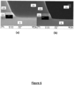
- the increased selectivity to the 5 ⁇ m CD mask 11b is shown to decrease the lateral etch rate of the mask, thereby reducing the loss in the critical dimension (CD).
- the reduced CD loss thereby permits steeper sidewall profiles as shown in figure 5 , and figures 6a , 6b , 7a and 7b .
- the 100 ⁇ m CD trenches have a shallower pre-etch mask profile than that of the 5 ⁇ m trenches, demonstrating that an increased BCl 3 flow rate compared with the Cl 2 flow rate, can impact a range of profiles and the CD of features.
- a common method of controlling the selectivity to underlayers of the workpiece 11 is through the use of a 'soft-landing' step which typically utilizes a lower platen bias to decrease the underlayer etch rate and the subsequent loss.
- BCl 3 has been reported above to increase the efficiency of AIScN etching, but as a result of the added sputter component of the boron, it is counter-intuitive to assume that its use would also decrease the etch rate of underlayers and increase the selectivity to these films.
- a similar workpiece was formed using a Si wafer substrate, but in this embodiment, the Al 0.7 Sc 0.3 N piezoelectric film 11a was replaced with a sputtered Mo film 11a' comprising an identical mask 11b to demonstrate the effect of the BCl 3 :Cl 2 flow rate ratio on the etch rate of the Mo film 11a'.
- the plasma generating device 17 is powered with approximately twice the electrical power during the primary (main) etch compared with the secondary (soft landing) etch.
- the platen 13 is powered with approximately 50% of the electrical power during the secondary etch compared with the primary etch.
- the pressure within the chamber during the secondary etch is almost double that compared with the primary etch.
- BCl 3 :Cl 2 flow rate ratios ⁇ 1:1 were found to be optimal for decreasing the etch rate of the Mo film 11a' and similarly increasing the AIScN selectivity to the Mo film 11a'.
- electrodes namely underlayers formed on the side of the substrate 11 opposite the piezoelectric film 11a, which etch readily in a chlorine-based chemistry, such as Mo
- decreasing the Cl 2 presence decreases the underlayer etch rate.
- the Cl 2 flow rate is decreased, so to does the AIScN etch rate, resulting in minimal changes to the underlayer selectivity.
- the AIScN:Mo selectivity can be increased by the same mechanism as previously described for photoresist.
- the increased BCl 3 :Cl 2 flow rate ratio reduces the Cl 2 presence, decreasing the Mo etch rate whilst the increased sputter component increases the AIScN etch rate, leading to an increased selectivity to the electrode. Ultimately this reduces the loss of the electrode when etching AIScN down to this metal film, as demonstrated in figure 8 .
- the platen power was decreased in the 1.5 and 2.125 BCl 3 :Cl 2 flow rate ratio tests (right two data points) to minimise the impact of increasing peak-peak voltage on the results.
- the process of etching a workpiece 11 comprising an AIScN film 11a on one side and a Mo film 11a' on the underside, therefore comprises a primary etching stage 100 for etching a trench through the AIScN film 11a and the majority of the Si substrate 11, and a secondary etching stage 200 which takes place immediately after the primary etching stage 100, and which is commenced prior to the trench extending out from the Si substrate.
- the secondary etching stage 200 comprises increasing the pressure in the chamber 12 at step 201, reducing the electrical power supplied to the antenna at step 202 and reducing the electrical bias to the platen at step 203.
- BCl 3 :Cl 2 flow rate ratio being ⁇ 1:1 it has been demonstrated above that a high AIScN (and AIYN and AlErN) etch rate (>170nm/min for 100 ⁇ m trenches and >250nm/min for 5 ⁇ m trenches) with improved selectivity to the photoresist and lower electrode metal can be achieved.
- the ⁇ 1:1 flow rate ratio would be applicable to all Al:Sc ratios, but due to the decreasing etch rate and increasing difficulty of etching AIN with higher percentages of doped scandium, the method becomes increasingly beneficial.
Landscapes
- Engineering & Computer Science (AREA)
- Physics & Mathematics (AREA)
- Plasma & Fusion (AREA)
- Chemical & Material Sciences (AREA)
- Analytical Chemistry (AREA)
- Manufacturing & Machinery (AREA)
- Drying Of Semiconductors (AREA)
- Plasma Technology (AREA)
Applications Claiming Priority (1)
| Application Number | Priority Date | Filing Date | Title |
|---|---|---|---|
| GBGB2117193.9A GB202117193D0 (en) | 2021-11-29 | 2021-11-29 | A method of plasma etching |
Publications (1)
| Publication Number | Publication Date |
|---|---|
| EP4192220A1 true EP4192220A1 (en) | 2023-06-07 |
Family
ID=80038579
Family Applications (1)
| Application Number | Title | Priority Date | Filing Date |
|---|---|---|---|
| EP22197203.7A Pending EP4192220A1 (en) | 2021-11-29 | 2022-09-22 | A method of plasma etching |
Country Status (7)
| Country | Link |
|---|---|
| US (1) | US20230170188A1 (https=) |
| EP (1) | EP4192220A1 (https=) |
| JP (1) | JP2023080017A (https=) |
| KR (1) | KR20230080304A (https=) |
| CN (1) | CN116190222A (https=) |
| GB (1) | GB202117193D0 (https=) |
| TW (1) | TW202321505A (https=) |
Families Citing this family (3)
| Publication number | Priority date | Publication date | Assignee | Title |
|---|---|---|---|---|
| EP4199687B1 (en) * | 2021-12-17 | 2024-04-10 | SPTS Technologies Limited | Plasma etching of additive-containing aln |
| GB202219567D0 (en) * | 2022-12-22 | 2023-02-08 | Spts Technologies Ltd | Method of plasma etching |
| CN117276076B (zh) * | 2023-11-09 | 2025-06-27 | 北京北方华创微电子装备有限公司 | 含Sc层的刻蚀方法、半导体器件及其制造方法及工艺设备 |
Family Cites Families (9)
| Publication number | Priority date | Publication date | Assignee | Title |
|---|---|---|---|---|
| WO2003021002A1 (en) * | 2001-08-29 | 2003-03-13 | Tokyo Electron Limited | Apparatus and method for plasma processing |
| JP4401641B2 (ja) * | 2001-11-07 | 2010-01-20 | 株式会社半導体エネルギー研究所 | 半導体装置の作製方法 |
| JP2008010611A (ja) * | 2006-06-29 | 2008-01-17 | Sony Corp | 半導体装置の製造方法および半導体装置 |
| KR20090086238A (ko) * | 2006-11-10 | 2009-08-11 | 에이전시 포 사이언스, 테크놀로지 앤드 리서치 | 마이크로기계 구조 및 마이크로기계 구조 제조방법 |
| JP2009055128A (ja) * | 2007-08-23 | 2009-03-12 | Nippon Dempa Kogyo Co Ltd | 薄膜圧電共振器の製造方法及び薄膜圧電共振器 |
| CN102280375B (zh) * | 2010-06-08 | 2013-10-16 | 中国科学院微电子研究所 | 一种先栅工艺中叠层金属栅结构的制备方法 |
| US20130119018A1 (en) * | 2011-11-15 | 2013-05-16 | Keren Jacobs Kanarik | Hybrid pulsing plasma processing systems |
| EP3539155A4 (en) * | 2016-11-10 | 2020-06-17 | The Government of the United States of America, as represented by the Secretary of the Navy | SCANDIUM-CONTAINING III-N ETCH STOP LAYERS FOR THE SELECTIVE ETCHING OF III-NITRIDES AND RELATED MATERIALS |
| US11173258B2 (en) * | 2018-08-30 | 2021-11-16 | Analog Devices, Inc. | Using piezoelectric electrodes as active surfaces for electroplating process |
-
2021
- 2021-11-29 GB GBGB2117193.9A patent/GB202117193D0/en not_active Ceased
-
2022
- 2022-09-19 TW TW111135278A patent/TW202321505A/zh unknown
- 2022-09-21 CN CN202211150597.9A patent/CN116190222A/zh active Pending
- 2022-09-22 EP EP22197203.7A patent/EP4192220A1/en active Pending
- 2022-10-17 KR KR1020220133294A patent/KR20230080304A/ko active Pending
- 2022-10-26 JP JP2022171258A patent/JP2023080017A/ja active Pending
- 2022-11-08 US US17/983,341 patent/US20230170188A1/en active Pending
Non-Patent Citations (5)
| Title |
|---|
| LOZZI ANDREA ET AL: "Al0.83Sc0.17N Contour-Mode Resonators With Electromechanical Coupling in Excess of 4.5%", IEEE TRANSACTIONS ON ULTRASONICS, FERROELECTRICS, AND FREQUENCY CONTROL, IEEE, USA, vol. 66, no. 1, 1 January 2019 (2019-01-01), pages 146 - 153, XP011705463, ISSN: 0885-3010, [retrieved on 20190114], DOI: 10.1109/TUFFC.2018.2882073 * |
| LUO ZHIFANG ET AL: "Optimization of AlN and AlScN Film ICP Etching", 2021 IEEE 34TH INTERNATIONAL CONFERENCE ON MICRO ELECTRO MECHANICAL SYSTEMS (MEMS), IEEE, 25 January 2021 (2021-01-25), pages 638 - 641, XP033887265, DOI: 10.1109/MEMS51782.2021.9375464 * |
| PETRICH R ET AL: "Investigation of ScAlN for piezoelectric and ferroelectric applications", 2019 22ND EUROPEAN MICROELECTRONICS AND PACKAGING CONFERENCE & EXHIBITION (EMPC), IMAPS-EUROPE, 16 September 2019 (2019-09-16), pages 1 - 5, XP033688817, DOI: 10.23919/EMPC44848.2019.8951824 * |
| SHAO SHUAI ET AL: "High Figure-of-Merit Lamb Wave Resonators Based on Al0.7Sc0.3N Thin Film", IEEE ELECTRON DEVICE LETTERS, IEEE, USA, vol. 42, no. 9, 26 July 2021 (2021-07-26), pages 1378 - 1381, XP011874254, ISSN: 0741-3106, [retrieved on 20210825], DOI: 10.1109/LED.2021.3100036 * |
| SPTS TECHNOLOGIES: "AlN/AlScN Etch for BAW Devices Typical Requirements", 1 February 2021 (2021-02-01), pages 1 - 2, XP093041572, Retrieved from the Internet <URL:https://www.spts.com/assets/media/aln-etch-for-baw-us-letter-feb2021.pdf> [retrieved on 20230424] * |
Also Published As
| Publication number | Publication date |
|---|---|
| GB202117193D0 (en) | 2022-01-12 |
| TW202321505A (zh) | 2023-06-01 |
| CN116190222A (zh) | 2023-05-30 |
| US20230170188A1 (en) | 2023-06-01 |
| KR20230080304A (ko) | 2023-06-07 |
| JP2023080017A (ja) | 2023-06-08 |
Similar Documents
| Publication | Publication Date | Title |
|---|---|---|
| EP4192220A1 (en) | A method of plasma etching | |
| CN109219867B (zh) | 蚀刻方法 | |
| JP4454148B2 (ja) | 改良式の酸化層エッチング方法 | |
| JP4657458B2 (ja) | 低容量の誘電体層をエッチングするための技術 | |
| JP5238704B2 (ja) | ハフニウム含有材料を乾式エッチングする方法およびシステム | |
| EP0702391B1 (en) | Etch processing and plasma reactor for performing same | |
| EP2423944A1 (en) | Plasma processing method and plasma processing apparatus | |
| WO2010047308A1 (ja) | プラズマエッチング方法及びプラズマエッチング装置 | |
| KR20200140388A (ko) | 패터닝을 위한 고품질 c 막들의 펄스형 플라즈마(dc/rf) 증착 | |
| KR100702726B1 (ko) | 플라즈마 에칭방법 및 플라즈마 처리장치 | |
| KR20180094801A (ko) | 플라즈마 처리 방법 및 플라즈마 처리 장치 | |
| TW201742143A (zh) | 蝕刻方法 | |
| EP4391023A1 (en) | Method of plasma etching | |
| TW200849325A (en) | Plasma processing method and plasma processing apparatus | |
| EP4199687B1 (en) | Plasma etching of additive-containing aln | |
| EP4704141A1 (en) | Method of plasma etching | |
| CN120202532A (zh) | 蚀刻方法和等离子体处理装置 | |
| JP3271373B2 (ja) | ドライエッチング方法 | |
| JP3252167B2 (ja) | ドライエッチング方法 | |
| US6908562B2 (en) | Method of forming electrode for saw device | |
| JP2675612B2 (ja) | プラズマエッチング装置 | |
| JP2000114239A (ja) | ドライエッチング方法及び装置 | |
| WO2000059024A1 (en) | Improved techniques for etching an aluminum neodymium-containing layer |
Legal Events
| Date | Code | Title | Description |
|---|---|---|---|
| PUAI | Public reference made under article 153(3) epc to a published international application that has entered the european phase |
Free format text: ORIGINAL CODE: 0009012 |
|
| STAA | Information on the status of an ep patent application or granted ep patent |
Free format text: STATUS: THE APPLICATION HAS BEEN PUBLISHED |
|
| AK | Designated contracting states |
Kind code of ref document: A1 Designated state(s): AL AT BE BG CH CY CZ DE DK EE ES FI FR GB GR HR HU IE IS IT LI LT LU LV MC MK MT NL NO PL PT RO RS SE SI SK SM TR |
|
| STAA | Information on the status of an ep patent application or granted ep patent |
Free format text: STATUS: REQUEST FOR EXAMINATION WAS MADE |
|
| 17P | Request for examination filed |
Effective date: 20231206 |
|
| RBV | Designated contracting states (corrected) |
Designated state(s): AL AT BE BG CH CY CZ DE DK EE ES FI FR GB GR HR HU IE IS IT LI LT LU LV MC MK MT NL NO PL PT RO RS SE SI SK SM TR |