EP4191799A1 - Circuit board assembly and electronic device - Google Patents
Circuit board assembly and electronic device Download PDFInfo
- Publication number
- EP4191799A1 EP4191799A1 EP21853798.3A EP21853798A EP4191799A1 EP 4191799 A1 EP4191799 A1 EP 4191799A1 EP 21853798 A EP21853798 A EP 21853798A EP 4191799 A1 EP4191799 A1 EP 4191799A1
- Authority
- EP
- European Patent Office
- Prior art keywords
- circuit board
- board
- bracket
- connector
- assembly according
- Prior art date
- Legal status (The legal status is an assumption and is not a legal conclusion. Google has not performed a legal analysis and makes no representation as to the accuracy of the status listed.)
- Granted
Links
Images


Classifications
-
- H—ELECTRICITY
- H01—ELECTRIC ELEMENTS
- H01R—ELECTRICALLY-CONDUCTIVE CONNECTIONS; STRUCTURAL ASSOCIATIONS OF A PLURALITY OF MUTUALLY-INSULATED ELECTRICAL CONNECTING ELEMENTS; COUPLING DEVICES; CURRENT COLLECTORS
- H01R12/00—Structural associations of a plurality of mutually-insulated electrical connecting elements, specially adapted for printed circuits, e.g. printed circuit boards [PCB], flat or ribbon cables, or like generally planar structures, e.g. terminal strips, terminal blocks; Coupling devices specially adapted for printed circuits, flat or ribbon cables, or like generally planar structures; Terminals specially adapted for contact with, or insertion into, printed circuits, flat or ribbon cables, or like generally planar structures
- H01R12/50—Fixed connections
- H01R12/51—Fixed connections for rigid printed circuits or like structures
- H01R12/52—Fixed connections for rigid printed circuits or like structures connecting to other rigid printed circuits or like structures
-
- H—ELECTRICITY
- H01—ELECTRIC ELEMENTS
- H01R—ELECTRICALLY-CONDUCTIVE CONNECTIONS; STRUCTURAL ASSOCIATIONS OF A PLURALITY OF MUTUALLY-INSULATED ELECTRICAL CONNECTING ELEMENTS; COUPLING DEVICES; CURRENT COLLECTORS
- H01R12/00—Structural associations of a plurality of mutually-insulated electrical connecting elements, specially adapted for printed circuits, e.g. printed circuit boards [PCB], flat or ribbon cables, or like generally planar structures, e.g. terminal strips, terminal blocks; Coupling devices specially adapted for printed circuits, flat or ribbon cables, or like generally planar structures; Terminals specially adapted for contact with, or insertion into, printed circuits, flat or ribbon cables, or like generally planar structures
- H01R12/70—Coupling devices
- H01R12/7005—Guiding, mounting, polarizing or locking means; Extractors
- H01R12/7011—Locking or fixing a connector to a PCB
- H01R12/707—Soldering or welding
-
- H—ELECTRICITY
- H01—ELECTRIC ELEMENTS
- H01R—ELECTRICALLY-CONDUCTIVE CONNECTIONS; STRUCTURAL ASSOCIATIONS OF A PLURALITY OF MUTUALLY-INSULATED ELECTRICAL CONNECTING ELEMENTS; COUPLING DEVICES; CURRENT COLLECTORS
- H01R12/00—Structural associations of a plurality of mutually-insulated electrical connecting elements, specially adapted for printed circuits, e.g. printed circuit boards [PCB], flat or ribbon cables, or like generally planar structures, e.g. terminal strips, terminal blocks; Coupling devices specially adapted for printed circuits, flat or ribbon cables, or like generally planar structures; Terminals specially adapted for contact with, or insertion into, printed circuits, flat or ribbon cables, or like generally planar structures
- H01R12/70—Coupling devices
- H01R12/71—Coupling devices for rigid printing circuits or like structures
- H01R12/712—Coupling devices for rigid printing circuits or like structures co-operating with the surface of the printed circuit or with a coupling device exclusively provided on the surface of the printed circuit
- H01R12/716—Coupling device provided on the PCB
-
- H—ELECTRICITY
- H05—ELECTRIC TECHNIQUES NOT OTHERWISE PROVIDED FOR
- H05K—PRINTED CIRCUITS; CASINGS OR CONSTRUCTIONAL DETAILS OF ELECTRIC APPARATUS; MANUFACTURE OF ASSEMBLAGES OF ELECTRICAL COMPONENTS
- H05K7/00—Constructional details common to different types of electric apparatus
- H05K7/02—Arrangements of circuit components or wiring on supporting structure
- H05K7/12—Resilient or clamping means for holding component to structure
-
- H—ELECTRICITY
- H01—ELECTRIC ELEMENTS
- H01R—ELECTRICALLY-CONDUCTIVE CONNECTIONS; STRUCTURAL ASSOCIATIONS OF A PLURALITY OF MUTUALLY-INSULATED ELECTRICAL CONNECTING ELEMENTS; COUPLING DEVICES; CURRENT COLLECTORS
- H01R12/00—Structural associations of a plurality of mutually-insulated electrical connecting elements, specially adapted for printed circuits, e.g. printed circuit boards [PCB], flat or ribbon cables, or like generally planar structures, e.g. terminal strips, terminal blocks; Coupling devices specially adapted for printed circuits, flat or ribbon cables, or like generally planar structures; Terminals specially adapted for contact with, or insertion into, printed circuits, flat or ribbon cables, or like generally planar structures
- H01R12/50—Fixed connections
- H01R12/51—Fixed connections for rigid printed circuits or like structures
-
- H—ELECTRICITY
- H01—ELECTRIC ELEMENTS
- H01R—ELECTRICALLY-CONDUCTIVE CONNECTIONS; STRUCTURAL ASSOCIATIONS OF A PLURALITY OF MUTUALLY-INSULATED ELECTRICAL CONNECTING ELEMENTS; COUPLING DEVICES; CURRENT COLLECTORS
- H01R12/00—Structural associations of a plurality of mutually-insulated electrical connecting elements, specially adapted for printed circuits, e.g. printed circuit boards [PCB], flat or ribbon cables, or like generally planar structures, e.g. terminal strips, terminal blocks; Coupling devices specially adapted for printed circuits, flat or ribbon cables, or like generally planar structures; Terminals specially adapted for contact with, or insertion into, printed circuits, flat or ribbon cables, or like generally planar structures
- H01R12/50—Fixed connections
- H01R12/51—Fixed connections for rigid printed circuits or like structures
- H01R12/52—Fixed connections for rigid printed circuits or like structures connecting to other rigid printed circuits or like structures
- H01R12/526—Fixed connections for rigid printed circuits or like structures connecting to other rigid printed circuits or like structures the printed circuits being on the same board
-
- H—ELECTRICITY
- H01—ELECTRIC ELEMENTS
- H01R—ELECTRICALLY-CONDUCTIVE CONNECTIONS; STRUCTURAL ASSOCIATIONS OF A PLURALITY OF MUTUALLY-INSULATED ELECTRICAL CONNECTING ELEMENTS; COUPLING DEVICES; CURRENT COLLECTORS
- H01R12/00—Structural associations of a plurality of mutually-insulated electrical connecting elements, specially adapted for printed circuits, e.g. printed circuit boards [PCB], flat or ribbon cables, or like generally planar structures, e.g. terminal strips, terminal blocks; Coupling devices specially adapted for printed circuits, flat or ribbon cables, or like generally planar structures; Terminals specially adapted for contact with, or insertion into, printed circuits, flat or ribbon cables, or like generally planar structures
- H01R12/70—Coupling devices
- H01R12/7005—Guiding, mounting, polarizing or locking means; Extractors
- H01R12/7011—Locking or fixing a connector to a PCB
-
- H—ELECTRICITY
- H01—ELECTRIC ELEMENTS
- H01R—ELECTRICALLY-CONDUCTIVE CONNECTIONS; STRUCTURAL ASSOCIATIONS OF A PLURALITY OF MUTUALLY-INSULATED ELECTRICAL CONNECTING ELEMENTS; COUPLING DEVICES; CURRENT COLLECTORS
- H01R12/00—Structural associations of a plurality of mutually-insulated electrical connecting elements, specially adapted for printed circuits, e.g. printed circuit boards [PCB], flat or ribbon cables, or like generally planar structures, e.g. terminal strips, terminal blocks; Coupling devices specially adapted for printed circuits, flat or ribbon cables, or like generally planar structures; Terminals specially adapted for contact with, or insertion into, printed circuits, flat or ribbon cables, or like generally planar structures
- H01R12/70—Coupling devices
- H01R12/71—Coupling devices for rigid printing circuits or like structures
-
- H—ELECTRICITY
- H01—ELECTRIC ELEMENTS
- H01R—ELECTRICALLY-CONDUCTIVE CONNECTIONS; STRUCTURAL ASSOCIATIONS OF A PLURALITY OF MUTUALLY-INSULATED ELECTRICAL CONNECTING ELEMENTS; COUPLING DEVICES; CURRENT COLLECTORS
- H01R12/00—Structural associations of a plurality of mutually-insulated electrical connecting elements, specially adapted for printed circuits, e.g. printed circuit boards [PCB], flat or ribbon cables, or like generally planar structures, e.g. terminal strips, terminal blocks; Coupling devices specially adapted for printed circuits, flat or ribbon cables, or like generally planar structures; Terminals specially adapted for contact with, or insertion into, printed circuits, flat or ribbon cables, or like generally planar structures
- H01R12/70—Coupling devices
- H01R12/71—Coupling devices for rigid printing circuits or like structures
- H01R12/712—Coupling devices for rigid printing circuits or like structures co-operating with the surface of the printed circuit or with a coupling device exclusively provided on the surface of the printed circuit
-
- H—ELECTRICITY
- H01—ELECTRIC ELEMENTS
- H01R—ELECTRICALLY-CONDUCTIVE CONNECTIONS; STRUCTURAL ASSOCIATIONS OF A PLURALITY OF MUTUALLY-INSULATED ELECTRICAL CONNECTING ELEMENTS; COUPLING DEVICES; CURRENT COLLECTORS
- H01R12/00—Structural associations of a plurality of mutually-insulated electrical connecting elements, specially adapted for printed circuits, e.g. printed circuit boards [PCB], flat or ribbon cables, or like generally planar structures, e.g. terminal strips, terminal blocks; Coupling devices specially adapted for printed circuits, flat or ribbon cables, or like generally planar structures; Terminals specially adapted for contact with, or insertion into, printed circuits, flat or ribbon cables, or like generally planar structures
- H01R12/70—Coupling devices
- H01R12/71—Coupling devices for rigid printing circuits or like structures
- H01R12/712—Coupling devices for rigid printing circuits or like structures co-operating with the surface of the printed circuit or with a coupling device exclusively provided on the surface of the printed circuit
- H01R12/714—Coupling devices for rigid printing circuits or like structures co-operating with the surface of the printed circuit or with a coupling device exclusively provided on the surface of the printed circuit with contacts abutting directly the printed circuit; Button contacts therefore provided on the printed circuit
-
- H—ELECTRICITY
- H01—ELECTRIC ELEMENTS
- H01R—ELECTRICALLY-CONDUCTIVE CONNECTIONS; STRUCTURAL ASSOCIATIONS OF A PLURALITY OF MUTUALLY-INSULATED ELECTRICAL CONNECTING ELEMENTS; COUPLING DEVICES; CURRENT COLLECTORS
- H01R12/00—Structural associations of a plurality of mutually-insulated electrical connecting elements, specially adapted for printed circuits, e.g. printed circuit boards [PCB], flat or ribbon cables, or like generally planar structures, e.g. terminal strips, terminal blocks; Coupling devices specially adapted for printed circuits, flat or ribbon cables, or like generally planar structures; Terminals specially adapted for contact with, or insertion into, printed circuits, flat or ribbon cables, or like generally planar structures
- H01R12/70—Coupling devices
- H01R12/71—Coupling devices for rigid printing circuits or like structures
- H01R12/72—Coupling devices for rigid printing circuits or like structures coupling with the edge of the rigid printed circuits or like structures
- H01R12/73—Coupling devices for rigid printing circuits or like structures coupling with the edge of the rigid printed circuits or like structures connecting to other rigid printed circuits or like structures
-
- H—ELECTRICITY
- H01—ELECTRIC ELEMENTS
- H01R—ELECTRICALLY-CONDUCTIVE CONNECTIONS; STRUCTURAL ASSOCIATIONS OF A PLURALITY OF MUTUALLY-INSULATED ELECTRICAL CONNECTING ELEMENTS; COUPLING DEVICES; CURRENT COLLECTORS
- H01R12/00—Structural associations of a plurality of mutually-insulated electrical connecting elements, specially adapted for printed circuits, e.g. printed circuit boards [PCB], flat or ribbon cables, or like generally planar structures, e.g. terminal strips, terminal blocks; Coupling devices specially adapted for printed circuits, flat or ribbon cables, or like generally planar structures; Terminals specially adapted for contact with, or insertion into, printed circuits, flat or ribbon cables, or like generally planar structures
- H01R12/70—Coupling devices
- H01R12/77—Coupling devices for flexible printed circuits, flat or ribbon cables or like structures
- H01R12/79—Coupling devices for flexible printed circuits, flat or ribbon cables or like structures connecting to rigid printed circuits or like structures
-
- H—ELECTRICITY
- H01—ELECTRIC ELEMENTS
- H01R—ELECTRICALLY-CONDUCTIVE CONNECTIONS; STRUCTURAL ASSOCIATIONS OF A PLURALITY OF MUTUALLY-INSULATED ELECTRICAL CONNECTING ELEMENTS; COUPLING DEVICES; CURRENT COLLECTORS
- H01R13/00—Details of coupling devices of the kinds covered by groups H01R12/70 or H01R24/00 - H01R33/00
- H01R13/62—Means for facilitating engagement or disengagement of coupling parts or for holding them in engagement
-
- H—ELECTRICITY
- H01—ELECTRIC ELEMENTS
- H01R—ELECTRICALLY-CONDUCTIVE CONNECTIONS; STRUCTURAL ASSOCIATIONS OF A PLURALITY OF MUTUALLY-INSULATED ELECTRICAL CONNECTING ELEMENTS; COUPLING DEVICES; CURRENT COLLECTORS
- H01R13/00—Details of coupling devices of the kinds covered by groups H01R12/70 or H01R24/00 - H01R33/00
- H01R13/62—Means for facilitating engagement or disengagement of coupling parts or for holding them in engagement
- H01R13/629—Additional means for facilitating engagement or disengagement of coupling parts, e.g. aligning or guiding means, levers, gas pressure electrical locking indicators, manufacturing tolerances
- H01R13/62983—Linear camming means or pivoting lever for connectors for flexible or rigid printed circuit boards, flat or ribbon cables
-
- H—ELECTRICITY
- H01—ELECTRIC ELEMENTS
- H01R—ELECTRICALLY-CONDUCTIVE CONNECTIONS; STRUCTURAL ASSOCIATIONS OF A PLURALITY OF MUTUALLY-INSULATED ELECTRICAL CONNECTING ELEMENTS; COUPLING DEVICES; CURRENT COLLECTORS
- H01R13/00—Details of coupling devices of the kinds covered by groups H01R12/70 or H01R24/00 - H01R33/00
- H01R13/62—Means for facilitating engagement or disengagement of coupling parts or for holding them in engagement
- H01R13/639—Additional means for holding or locking coupling parts together, after engagement, e.g. separate keylock, retainer strap
Definitions
- This application relates to the field of electronic device technologies, and in particular, to a circuit board assembly and an electronic device.
- a circuit board of a camera module in a mobile phone is connected to a mainboard of the electronic device by typically using a board-to-board connector, while the board-to-board connector needs to be fastened to the mainboard with screws.
- Embodiments of this application provides a circuit board assembly and an electronic device, which can resolve the problem of insecure connection between a board-to-board connector and a circuit board.
- an embodiment of this application provides a circuit board assembly, including:
- an embodiment of this application further provides an electronic device, including the foregoing circuit board assembly, where the circuit board is a mainboard of the electronic device.
- the fixing member is used to fasten the first bracket and the second bracket to the circuit board, which can improve firmness of the connection of the neighboring area of the first bracket and the second bracket to the circuit board.
- the fewer screw mounting holes can be provided in the circuit board, improving utilization of the circuit board.
- circuit board assembly including:
- the board-to-board connectors are mounted onto the circuit board 10 in chronological order. Therefore, a board-to-board connector that needs to be installed earlier may be set as the first board-to-board connector 11, and a board-to-board connector that needs to be installed later may be set as the second board-to-board connector 12, and then the first bracket 20 and the second bracket 30 are used to fasten the first board-to-board connector 11 and the second board-to-board connector 12 respectively.
- the first bracket 20 and the second bracket 30 may be fastened on the circuit board 10 with screws, so as to fasten the first board-to-board connector 11 and the second board-to-board connector 12, ensuring stability of connection of the first board-to-board connector 11 and the second board-to-board connector 12 to the circuit board 10.
- the fixing member 40 is used to fasten the first bracket 20 and the second bracket 30 to the circuit board 10, which can improve firmness of the connection of the neighboring area of the first bracket 20 and the second bracket 30 to the circuit board 10.
- fewer screw connection structures are used, fewer screw mounting holes can be provided in the circuit board 10, improving utilization of the circuit board 10.
- the fixing member 40 is provided with the slot 41, and the escape hole 21 is provided on a side of the first bracket 20 neighboring to the second bracket 30, so that the slot 41 can extend out from the escape hole 21.
- the tongue insert 31 may be disposed on a side of the second bracket 30 neighboring to the first bracket 20 and at least part of the tongue insert 31 can be inserted into the slot 41, and through cooperation of the slot 41 and the tongue insert 31, the escape hole 40 is snap-fitted with the second bracket 30. As the tongue insert extends out from the escape hole 21, the first bracket 20 can be fastened as well.
- the fixing member 40 fastens the first bracket 20 and the second bracket 30 on the circuit board.
- circuit board assembly can not only provide firm and reliable connection between board-to-board connectors and the circuit board, but also have a simple and compact structure, occupying a small space.
- the fixing member 40 includes a base plate 42 and a clip hook 43, where the base plate 42 is connected to the circuit board 10, the clip hook 43 is disposed on a side of the base plate 42 away from the circuit board 10, and the slot 41 is formed between the clip hook 43 and the base plate 42.
- the slot 41 is formed through the provision of the clip hook 43, such that the tongue insert 31 can be inserted into the slot 41 and snap-fitted with the clip hook 43, enabling the fixing member 40 to fasten the first bracket 20 and the second bracket 30.
- the clip hook 43 includes a connecting plate 431 and a fixing plate 432, where the connecting plate 431 is connected to the base plate 42, the connecting plate 431 extends away from the circuit board 10, the fixing plate 432 is connected to an end of the connecting plate 431 away from the circuit board 10, and the fixing plate 432 extends toward the tongue insert 31, so as to form the slot 41 between the base plate 42, the connecting plate 431, and the fixing plate 432.
- a guiding face may be provided at an inserting end of the tongue insert 31, or a guiding face may be provided on a side of the fixing plate 432 facing toward the base plate 42.
- the fixing plate 432 may extend away from the circuit board 10, so that an opening size of the slot 41 is gradually reduced in a direction approaching the connecting plate 431, making it easy to insert the tongue insert 31 into the slot 41.
- the opening size of the slot 41 is gradually reduced in the direction approaching the connecting plate 431, the connection between the tongue insert 31 and the slot 41 is more reliable and more secure when the tongue insert 31 is completely inserted into the slot 41.
- the circuit board 10 is provided with a mounting hole 13
- a connecting pin 44 is provided on a side of the base plate 42 facing toward the circuit board 10, and the connecting pin 44 is mounted inside the mounting hole 13, so as to fasten the fixing member 40 on the circuit board 10.
- the connecting pin 44 may be connected to the circuit board 10 by welding. Specifically, the connecting pin 44 may extend into the mounting hole 13 and be soldered with solder paste to ensure a strong tensile strength between the fixing member 40 and the circuit board 10, increasing structural reliability of the circuit board assembly.
- the mounting hole 13 may be a strip-shaped hole and a length direction of the mounting hole 13 extends along a trace outgoing direction of a processor (not shown in the figure) on the circuit board 10, so that a wiring space occupied by the mounting hole 13 in the circuit board 10 is reduced, further improving utilization of the circuit board 10.
- the mounting hole 13 is 0.4 mm-0.6 mm in width and 1.2 mm-1.8 mm in length, which can effectively reduce the space occupied by the mounting hole 13 on the circuit board 10 as compared with a screw hole with a diameter of 1.6 mm in the circuit board 10.
- the mounting hole 13 may be designed as a rectangular hole 1.5 mm long and 0.5 mm wide, so as to reduce the space occupied by the mounting hole 13 in the circuit board 10.
- the first bracket 20 is provided with a sunken portion 22, where the sunken portion 22 faces toward the circuit board 10, the sunken portion 22 is located between the escape hole 21 and a body structure of the second bracket 20, and the sunken portion 22 abuts against a side of the tongue insert 31 facing toward the circuit board 10.
- the first bracket 20 is provided with the sunken portion 22 such that the escape hole 21 for extending of the slot 41 is formed in the first bracket 20, and the sunken portion 22 is located between the tongue insert 31 and the base plate 42.
- the fixing member 40 can also function to fasten the first bracket 20, achieving the purpose of using the fixing member 40 to fasten the first bracket 20 and the second bracket 30.
- the provision of the sunken portion 22 allows the forming of the escape hole 21 for extending of the slot 41, reducing the size of the fixing member 40 in a thickness direction of the circuit board, thereby achieving the purpose of easy spatial layout and weight reduction.
- the sunken portion 22 and tongue insert 31 are stacked on the base plate 42 in sequence and the tongue insert 31 is snap-fitted with the slot 41, so as to fasten the first bracket 20 and the second bracket 30 using the fixing member 40, which also improves reliability of the connection of the neighboring area of the first bracket 20 and the second bracket 30 to the circuit board 10.
- the second bracket 30 is provided with a transition portion 32 connecting to the tongue insert 31, where the transition portion 32 extends, in a direction facing toward the tongue insert 31, toward the circuit board 10
- the transition portion 32 extending, in the direction facing the tongue insert 31, toward the circuit board 10 can reduce the size of the fixing member 40 in the thickness direction of the circuit board, so as to achieve the purpose of easy space layout and weight reduction.
- the first board-to-board connector 11 may be provided in plurality, and the plurality of first board-to-board connectors 11 may be arranged along a first direction; and the second board-to-board connector 12 may also be provided in plurality and the plurality of second board-to-board connectors 12 may be arranged along a second direction, where an included angle between the first direction and the second direction is greater than 0°, and one first board-to-board connector 11 and one second board-to-board connector 12 are located respectively on two opposite sides of the fixing member 40.
- the mixing member 40 fastens the two board-to-board connectors, improving fastening efficiency of the fixing member 40.
- this also reduces use of screw connection structures and therefore reduces screw mounting holes provided in the circuit board 10, improving utilization of the circuit board 10.
- the included angle between the first direction and the second direction may be 90°, such that the first board-to-board connector 11 and the second board-to-board connector 12 can be better arranged on the circuit board 10.
- the second board-to-board connector 12 includes a fingerprint module board-to-board connector, so that the finger module board-to-board connector can be better mounted on the circuit board 10.
- Both the first bracket 20 and the second bracket 30 are provided with a screw hole, and the circuit board 10 is also provided with through-holes fitting the screw holes, such that the first bracket 20 and the second bracket 30 can be mounted on the circuit board 10 with screws.
- the fixing member 40 is used to fasten the first bracket 20 and the second bracket 30 to the circuit board 10.
- An embodiment of this application further provides an electronic device, including the foregoing circuit board assembly, where the circuit board is a mainboard of the electronic device. It should be note that the implementations of the embodiment of the circuit board assembly are also applicable to the embodiment of the electronic device, with the same technical effects achieved. Details are not described herein again.
Landscapes
- Engineering & Computer Science (AREA)
- Microelectronics & Electronic Packaging (AREA)
- Mounting Of Printed Circuit Boards And The Like (AREA)
- Coupling Device And Connection With Printed Circuit (AREA)
- Mounting Components In General For Electric Apparatus (AREA)
Abstract
Description
- This application claims priority to
Chinese Patent Application No. 202010767024.5, in China filed on August 03, 2020 - This application relates to the field of electronic device technologies, and in particular, to a circuit board assembly and an electronic device.
- At present, electronic devices have been developing toward being light and thin and integrating more and more functions inside. As a result, a space for mounting functional devices that implement various functions becomes increasingly small. For example, a circuit board of a camera module in a mobile phone is connected to a mainboard of the electronic device by typically using a board-to-board connector, while the board-to-board connector needs to be fastened to the mainboard with screws.
- However, with an increasing number of board-to-board connectors in electronic devices, the way of fastening with screws leads to many screw holes in the circuit board, while arrangement of the screw holes affects the trace layout. Guarantee of trace layout for important chips on the mainboard results in insecure connection between the board-to-board connectors and the circuit board.
- Embodiments of this application provides a circuit board assembly and an electronic device, which can resolve the problem of insecure connection between a board-to-board connector and a circuit board.
- To resolve the foregoing technical problem, this application is implemented as follows:
- According to a first aspect, an embodiment of this application provides a circuit board assembly, including:
- a circuit board to which a first board-to-board connector and a second board-to-board connector are mounted;
- a first bracket, where the first bracket is mounted on the circuit board, the first bracket is located on a side of the first board-to-board connector away from the circuit board, the first bracket is configured to fasten the first board-to-board connector, and the first bracket is provided with an escape hole;
- a second bracket, where the second bracket is mounted on the circuit board, the second bracket is located on a side of the second board-to-board connector away from the circuit board, the second bracket is configured to fasten the second board-to-board connector, the second bracket is disposed neighboring to the first bracket, and the second bracket is provided with a tongue insert, the tongue insert being located on a side of the second bracket facing toward the first bracket; and
- a fixing member, where the fixing member is connected to the circuit board and the fixing member is provided with a slot, the slot extending out from the escape hole and at least part of the tongue insert being inserted into the slot.
- According to a second aspect, an embodiment of this application further provides an electronic device, including the foregoing circuit board assembly, where the circuit board is a mainboard of the electronic device.
- In embodiments of this application, for a neighboring area of the first bracket and the second bracket, the fixing member is used to fasten the first bracket and the second bracket to the circuit board, which can improve firmness of the connection of the neighboring area of the first bracket and the second bracket to the circuit board. In addition, as fewer screw connection structures are used, the fewer screw mounting holes can be provided in the circuit board, improving utilization of the circuit board.
-
-
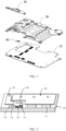
FIG. 1 is an exploded view of a circuit board assembly according to an embodiment of this application; -
FIG. 2 is a cross-sectional diagram of a circuit board assembly according to an embodiment of this application; -
FIG. 3 is a three-dimensional diagram of a fixing member according to an embodiment of this application; -
FIG. 4 is a schematic structural diagram of a circuit board assembly according to an embodiment of this application; -
FIG. 5 is a local enlarged view of area A inFIG. 4 ; -
FIG. 6 is a schematic structural diagram of a first bracket according to an embodiment of this application; -
FIG. 7 is a local enlarged view of area B inFIG. 6 ; and -
FIG. 8 is a schematic structural diagram of a second bracket according to an embodiment of this application. - The following clearly and completely describes the technical solutions in the embodiments of this application with reference to the accompanying drawings in the embodiments of this application. Apparently, the described embodiments are some but not all of the embodiments of this application. All other embodiments obtained by a person of ordinary skill in the art based on the embodiments of this application without creative efforts shall fall within the protection scope of this application.
- In the specification and the claims of this application, the terms "first", "second", and so on are intended to distinguish between different objects but do not describe a specific order or sequence. It should be understood that data used in this way is used interchangeably in appropriate circumstances so that the embodiments of this application can be implemented in other orders than the order illustrated or described herein. In addition, in this specification and claims, "and/or" represents at least one of the objects connected, and the symbol "/" generally represents an "or" relationship between the associated objects.
- As shown in
FIG. 1 and FIG. 2 , an embodiment of this application provides a circuit board assembly, including: - a
circuit board 10 to which a first board-to-board connector 11 and a second board-to-board connector 12 are mounted; - a
first bracket 20, where thefirst bracket 20 is mounted on thecircuit board 10, thefirst bracket 20 is located on a side of the first board-to-board connector 11 away from thecircuit board 10, thefirst bracket 20 is configured to fasten the first board-to-board connector 11, and thefirst bracket 20 is provided with anescape hole 21; - a
second bracket 30, where thesecond bracket 30 is mounted on thecircuit board 10, thesecond bracket 30 is located on a side of the second board-to-board connector 12 away from thecircuit board 10, thesecond bracket 30 is configured to fasten the second board-to-board connector 12, thesecond bracket 30 is disposed neighboring to thefirst bracket 20, and thesecond bracket 30 is provided with a tongue insert 31, the tongue insert 31 being located on a side of thesecond bracket 30 facing toward thefirst bracket 20; and - a
fixing member 40, where thefixing member 40 is connected to thecircuit board 10 and thefixing member 40 is provided with a slot 41, the slot 41 extending out from theescape hole 21 and at least part of the tongue insert 31 being inserted into the slot 41. - In this implementation, for the board-to-board connectors mounted on the
circuit board 10, as each of the board-to-board connectors corresponds to a different functional component, the board-to-board connectors are mounted onto thecircuit board 10 in chronological order. Therefore, a board-to-board connector that needs to be installed earlier may be set as the first board-to-board connector 11, and a board-to-board connector that needs to be installed later may be set as the second board-to-board connector 12, and then thefirst bracket 20 and thesecond bracket 30 are used to fasten the first board-to-board connector 11 and the second board-to-board connector 12 respectively. - The
first bracket 20 and thesecond bracket 30 may be fastened on thecircuit board 10 with screws, so as to fasten the first board-to-board connector 11 and the second board-to-board connector 12, ensuring stability of connection of the first board-to-board connector 11 and the second board-to-board connector 12 to thecircuit board 10. - In addition, for a neighboring area of the
first bracket 20 and thesecond bracket 30, thefixing member 40 is used to fasten thefirst bracket 20 and thesecond bracket 30 to thecircuit board 10, which can improve firmness of the connection of the neighboring area of thefirst bracket 20 and thesecond bracket 30 to thecircuit board 10. In addition, as fewer screw connection structures are used, fewer screw mounting holes can be provided in thecircuit board 10, improving utilization of thecircuit board 10. - The
fixing member 40 is provided with the slot 41, and theescape hole 21 is provided on a side of thefirst bracket 20 neighboring to thesecond bracket 30, so that the slot 41 can extend out from theescape hole 21. The tongue insert 31 may be disposed on a side of thesecond bracket 30 neighboring to thefirst bracket 20 and at least part of thetongue insert 31 can be inserted into the slot 41, and through cooperation of the slot 41 and the tongue insert 31, theescape hole 40 is snap-fitted with thesecond bracket 30. As the tongue insert extends out from theescape hole 21, thefirst bracket 20 can be fastened as well. Thus, thefixing member 40 fastens thefirst bracket 20 and thesecond bracket 30 on the circuit board. - It can be seen that the circuit board assembly according to the embodiment of this application can not only provide firm and reliable connection between board-to-board connectors and the circuit board, but also have a simple and compact structure, occupying a small space.
- Optionally, as shown in
FIG. 3 , thefixing member 40 includes abase plate 42 and aclip hook 43, where thebase plate 42 is connected to thecircuit board 10, theclip hook 43 is disposed on a side of thebase plate 42 away from thecircuit board 10, and the slot 41 is formed between theclip hook 43 and thebase plate 42. - In this implementation, the slot 41 is formed through the provision of the
clip hook 43, such that thetongue insert 31 can be inserted into the slot 41 and snap-fitted with theclip hook 43, enabling thefixing member 40 to fasten thefirst bracket 20 and thesecond bracket 30. - The
clip hook 43 includes a connectingplate 431 and afixing plate 432, where the connectingplate 431 is connected to thebase plate 42, the connectingplate 431 extends away from thecircuit board 10, thefixing plate 432 is connected to an end of the connectingplate 431 away from thecircuit board 10, and thefixing plate 432 extends toward thetongue insert 31, so as to form the slot 41 between thebase plate 42, the connectingplate 431, and thefixing plate 432. - In this way, the
tongue insert 31 is inserted into the slot 41 so as to be snap-fitted with thefixing plate 432, enabling thefixing member 40 to fasten thefirst bracket 20 and thesecond bracket 30. In addition, to make it easy to insert the tongue insert 31 into the slot 41, a guiding face may be provided at an inserting end of the tongue insert 31, or a guiding face may be provided on a side of thefixing plate 432 facing toward thebase plate 42. - Further, the
fixing plate 432 may extend away from thecircuit board 10, so that an opening size of the slot 41 is gradually reduced in a direction approaching the connectingplate 431, making it easy to insert the tongue insert 31 into the slot 41. In addition, because the opening size of the slot 41 is gradually reduced in the direction approaching the connectingplate 431, the connection between the tongue insert 31 and the slot 41 is more reliable and more secure when thetongue insert 31 is completely inserted into the slot 41. - As shown in
FIG. 4 andFIG. 5 , thecircuit board 10 is provided with amounting hole 13, a connectingpin 44 is provided on a side of thebase plate 42 facing toward thecircuit board 10, and the connectingpin 44 is mounted inside themounting hole 13, so as to fasten thefixing member 40 on thecircuit board 10. - The connecting
pin 44 may be connected to thecircuit board 10 by welding. Specifically, the connectingpin 44 may extend into themounting hole 13 and be soldered with solder paste to ensure a strong tensile strength between thefixing member 40 and thecircuit board 10, increasing structural reliability of the circuit board assembly. - Optionally, the
mounting hole 13 may be a strip-shaped hole and a length direction of themounting hole 13 extends along a trace outgoing direction of a processor (not shown in the figure) on thecircuit board 10, so that a wiring space occupied by themounting hole 13 in thecircuit board 10 is reduced, further improving utilization of thecircuit board 10. - The
mounting hole 13 is 0.4 mm-0.6 mm in width and 1.2 mm-1.8 mm in length, which can effectively reduce the space occupied by themounting hole 13 on thecircuit board 10 as compared with a screw hole with a diameter of 1.6 mm in thecircuit board 10. - In a specific implementation of this application, the
mounting hole 13 may be designed as a rectangular hole 1.5 mm long and 0.5 mm wide, so as to reduce the space occupied by themounting hole 13 in thecircuit board 10. - Optionally, as shown in
FIG. 6 andFIG. 7 , thefirst bracket 20 is provided with asunken portion 22, where thesunken portion 22 faces toward thecircuit board 10, thesunken portion 22 is located between theescape hole 21 and a body structure of thesecond bracket 20, and thesunken portion 22 abuts against a side of thetongue insert 31 facing toward thecircuit board 10. - In this implementation, the
first bracket 20 is provided with thesunken portion 22 such that theescape hole 21 for extending of the slot 41 is formed in thefirst bracket 20, and thesunken portion 22 is located between thetongue insert 31 and thebase plate 42. In this way, the fixingmember 40 can also function to fasten thefirst bracket 20, achieving the purpose of using the fixingmember 40 to fasten thefirst bracket 20 and thesecond bracket 30. - In addition, the provision of the
sunken portion 22 allows the forming of theescape hole 21 for extending of the slot 41, reducing the size of the fixingmember 40 in a thickness direction of the circuit board, thereby achieving the purpose of easy spatial layout and weight reduction. - In this way, in a position in which the fixing
member 40 is located, thesunken portion 22 and tongue insert 31 are stacked on thebase plate 42 in sequence and thetongue insert 31 is snap-fitted with the slot 41, so as to fasten thefirst bracket 20 and thesecond bracket 30 using the fixingmember 40, which also improves reliability of the connection of the neighboring area of thefirst bracket 20 and thesecond bracket 30 to thecircuit board 10. - Optionally, as shown in
FIG. 8 , thesecond bracket 30 is provided with atransition portion 32 connecting to thetongue insert 31, where thetransition portion 32 extends, in a direction facing toward thetongue insert 31, toward thecircuit board 10 - In this implementation, the
transition portion 32 extending, in the direction facing thetongue insert 31, toward thecircuit board 10 can reduce the size of the fixingmember 40 in the thickness direction of the circuit board, so as to achieve the purpose of easy space layout and weight reduction. - As shown in
FIG. 4 , the first board-to-board connector 11 may be provided in plurality, and the plurality of first board-to-board connectors 11 may be arranged along a first direction; and the second board-to-board connector 12 may also be provided in plurality and the plurality of second board-to-board connectors 12 may be arranged along a second direction, where an included angle between the first direction and the second direction is greater than 0°, and one first board-to-board connector 11 and one second board-to-board connector 12 are located respectively on two opposite sides of the fixingmember 40. - Thus, with one first board-to-
board connector 11 and one second board-to-board connector 12 disposed on each of the two opposite sides of the fixingmember 40, the mixingmember 40 fastens the two board-to-board connectors, improving fastening efficiency of the fixingmember 40. In addition, this also reduces use of screw connection structures and therefore reduces screw mounting holes provided in thecircuit board 10, improving utilization of thecircuit board 10. - Optionally, the included angle between the first direction and the second direction may be 90°, such that the first board-to-
board connector 11 and the second board-to-board connector 12 can be better arranged on thecircuit board 10. - The second board-to-
board connector 12 includes a fingerprint module board-to-board connector, so that the finger module board-to-board connector can be better mounted on thecircuit board 10. - Both the
first bracket 20 and thesecond bracket 30 are provided with a screw hole, and thecircuit board 10 is also provided with through-holes fitting the screw holes, such that thefirst bracket 20 and thesecond bracket 30 can be mounted on thecircuit board 10 with screws. In addition, in the neighboring area of thefirst bracket 20 and thesecond bracket 30, the fixingmember 40 is used to fasten thefirst bracket 20 and thesecond bracket 30 to thecircuit board 10. - An embodiment of this application further provides an electronic device, including the foregoing circuit board assembly, where the circuit board is a mainboard of the electronic device. It should be note that the implementations of the embodiment of the circuit board assembly are also applicable to the embodiment of the electronic device, with the same technical effects achieved. Details are not described herein again.
- It should be noted that, in this specification, the terms "include", "comprise", or any of their variants are intended to cover a non-exclusive inclusion, such that a process, method, article, or apparatus that includes a series of elements not only includes those elements but also includes other elements that are not expressly listed, or further includes elements inherent to such process, method, article, or apparatus. In the absence of more restrictions, an element defined by "including a... " does not exclude the presence of another same element in a process, method, article, or apparatus that includes that element.
- Embodiments of this application have been described above with reference to the accompanying drawings. However, this application is not limited to these specific embodiments. The foregoing specific embodiments are merely illustrative rather than restrictive. As inspired by this application, a person of ordinary skill in the art may develop many other forms that are not departing from the principle of this application and the protection scope of the claims, and all such forms fall within the protection scope of this application.
Claims (11)
- A circuit board assembly, comprising:a circuit board to which a first board-to-board connector and a second board-to-board connector are mounted;a first bracket, wherein the first bracket is mounted on the circuit board, the first bracket is located on a side of the first board-to-board connector away from the circuit board, the first bracket is configured to fasten the first board-to-board connector, and the first bracket is provided with an escape hole;a second bracket, wherein the second bracket is mounted on the circuit board, the second bracket is located on a side of the second board-to-board connector away from the circuit board, the second bracket is configured to fasten the second board-to-board connector, the second bracket is disposed neighboring to the first bracket, and the second bracket is provided with a tongue insert, the tongue insert being located on a side of the second bracket facing toward the first bracket; anda fixing member, wherein the fixing member is connected to the circuit board and the fixing member is provided with a slot, the slot extending out from the escape hole and at least part of the tongue insert being inserted into the slot.
- The circuit board assembly according to claim 1, wherein the fixing member comprises a base plate and a clip hook, the base plate being connected to the circuit board, the clip hook being disposed on a side of the base plate away from the circuit board, and the slot being formed between the clip hook and the base plate.
- The circuit board assembly according to claim 2, wherein the circuit board is provided with a mounting hole, a connecting pin is provided on a side of the base plate facing toward the circuit board, and the connecting pin is mounted inside the mounting hole, so as to mount the fixing member on the circuit board.
- The circuit board assembly according to claim 3, wherein the connecting pin is joined to the circuit board by welding.
- The circuit board assembly according to claim 3, wherein the mounting hole is a strip-shaped hole and a length direction of the mounting hole extends along a trace outgoing direction of a processor on the circuit board.
- The circuit board assembly according to claim 2, wherein the clip hook comprises a connecting plate and a fixing plate, the connecting plate being connected to the base plate, the connecting plate extending away from the circuit board, the fixing plate being connected to an end of the connecting plate away from the circuit board, and the fixing plate extending toward the tongue insert, so as to form the slot between the base plate, the connecting plate, and the fixing plate.
- The circuit board assembly according to claim 6, wherein the fixing plate extends away from the circuit board, so that an opening size of the slot is gradually reduced in a direction approaching the connecting plate.
- The circuit board assembly according to claim 1, wherein the second bracket is provided with a transition portion connecting to the tongue insert, the transition portion extending, in a direction facing the tongue insert, toward the circuit board.
- The circuit board assembly according to claim 1, wherein the first bracket is provided with a sunken portion, the sunken portion facing toward the circuit board, the sunken portion being located between the escape hole and the second bracket, and the sunken portion abutting against a side of the tongue insert facing toward the circuit board.
- The circuit board assembly according to claim 1, wherein the first board-to-board connector is provided in plurality, and the plurality of first board-to-board connectors are arranged along a first direction; the second board-to-board connector is provided in plurality, and the plurality of second board-to-board connectors are arranged along a second direction; and an included angle between the first direction and the second direction is greater than 0°, wherein one of the first board-to-board connectors and one of the second board-to-board connectors are respectively located on two opposite sides of the fixing portion.
- An electronic device, comprising the circuit board assembly according to any one of claims 1 to 10, wherein the circuit board is a mainboard of the electronic device.
Applications Claiming Priority (2)
| Application Number | Priority Date | Filing Date | Title |
|---|---|---|---|
| CN202010767024.5A CN111834814B (en) | 2020-08-03 | 2020-08-03 | Circuit board assemblies and electronic equipment |
| PCT/CN2021/110018 WO2022028357A1 (en) | 2020-08-03 | 2021-08-02 | Circuit board assembly and electronic device |
Publications (3)
| Publication Number | Publication Date |
|---|---|
| EP4191799A1 true EP4191799A1 (en) | 2023-06-07 |
| EP4191799A4 EP4191799A4 (en) | 2024-01-17 |
| EP4191799B1 EP4191799B1 (en) | 2026-01-28 |
Family
ID=72919363
Family Applications (1)
| Application Number | Title | Priority Date | Filing Date |
|---|---|---|---|
| EP21853798.3A Active EP4191799B1 (en) | 2020-08-03 | 2021-08-02 | Circuit board assembly and electronic device |
Country Status (6)
| Country | Link |
|---|---|
| US (1) | US12531357B2 (en) |
| EP (1) | EP4191799B1 (en) |
| JP (1) | JP7589333B2 (en) |
| KR (1) | KR102765226B1 (en) |
| CN (1) | CN111834814B (en) |
| WO (1) | WO2022028357A1 (en) |
Families Citing this family (1)
| Publication number | Priority date | Publication date | Assignee | Title |
|---|---|---|---|---|
| CN111834814B (en) * | 2020-08-03 | 2021-07-23 | 维沃移动通信有限公司 | Circuit board assemblies and electronic equipment |
Family Cites Families (10)
| Publication number | Priority date | Publication date | Assignee | Title |
|---|---|---|---|---|
| CN2745247Y (en) * | 2004-09-16 | 2005-12-07 | 鸿富锦精密工业(深圳)有限公司 | Connector fixer |
| CN103124484B (en) * | 2011-11-21 | 2017-01-25 | 富泰华工业(深圳)有限公司 | Electronic device |
| JP5884813B2 (en) * | 2013-11-21 | 2016-03-15 | Smk株式会社 | Electrical connector |
| CN206353647U (en) * | 2016-12-29 | 2017-07-25 | 维沃移动通信有限公司 | A kind of pressing structure and mobile terminal of BTB connectors |
| CN206922075U (en) * | 2017-05-12 | 2018-01-23 | 广东欧珀移动通信有限公司 | Connector assembly, power supply module and mobile terminal |
| CN107086384B (en) | 2017-05-12 | 2019-12-06 | Oppo广东移动通信有限公司 | Connector assembly, power supply assembly and mobile terminal |
| CN108307585B (en) * | 2018-01-24 | 2020-02-11 | Oppo广东移动通信有限公司 | Electronic equipment and circuit board assembly thereof |
| CN108321568B (en) * | 2018-01-24 | 2020-03-10 | Oppo广东移动通信有限公司 | Electronic equipment and circuit board assembly thereof |
| CN210007023U (en) * | 2019-04-24 | 2020-01-31 | 西安易朴通讯技术有限公司 | Connector locking structure and mobile terminal |
| CN111834814B (en) * | 2020-08-03 | 2021-07-23 | 维沃移动通信有限公司 | Circuit board assemblies and electronic equipment |
-
2020
- 2020-08-03 CN CN202010767024.5A patent/CN111834814B/en active Active
-
2021
- 2021-08-02 WO PCT/CN2021/110018 patent/WO2022028357A1/en not_active Ceased
- 2021-08-02 EP EP21853798.3A patent/EP4191799B1/en active Active
- 2021-08-02 KR KR1020227043909A patent/KR102765226B1/en active Active
- 2021-08-02 JP JP2023507505A patent/JP7589333B2/en active Active
-
2023
- 2023-02-01 US US18/104,732 patent/US12531357B2/en active Active
Also Published As
| Publication number | Publication date |
|---|---|
| JP7589333B2 (en) | 2024-11-25 |
| WO2022028357A1 (en) | 2022-02-10 |
| JP2023537710A (en) | 2023-09-05 |
| EP4191799B1 (en) | 2026-01-28 |
| KR20230010732A (en) | 2023-01-19 |
| CN111834814B (en) | 2021-07-23 |
| US20230178909A1 (en) | 2023-06-08 |
| EP4191799A4 (en) | 2024-01-17 |
| US12531357B2 (en) | 2026-01-20 |
| CN111834814A (en) | 2020-10-27 |
| KR102765226B1 (en) | 2025-02-06 |
Similar Documents
| Publication | Publication Date | Title |
|---|---|---|
| EP2945470B1 (en) | Circuit board interconnection architecture | |
| TWI423536B (en) | Connector mechanism for connecting a board card | |
| US8092262B1 (en) | Eye-of-the needle pin of an electrical contact | |
| US20110294309A1 (en) | Expansion card and expansion apparatus thereof | |
| US8559189B2 (en) | Riser card for power supply | |
| JP2002259051A (en) | Combined structure of touch controller and LCD module controller in touch panel integrated LCD | |
| JPH08222870A (en) | Printed circuit board mounting device | |
| US7794233B1 (en) | Flexible circuit member for electrically coupling connectors with one another | |
| US20120214347A1 (en) | Edge Connector That Accommodates Printed Circuit Boards Of Varying Thickness | |
| CN115250304B (en) | Terminal Equipment | |
| US12531357B2 (en) | Circuit board assembly with interconnecting fixing brackets holding board-to-board connectors to a circuit board and a device using the same | |
| US6473043B1 (en) | Antenna assembly | |
| US7309240B2 (en) | Apparatus and electronic apparatus | |
| CN108922407B (en) | Display screens and display devices | |
| US20090040713A1 (en) | Server enclosure | |
| CN211128697U (en) | Electronic device | |
| EP4117258A1 (en) | Electronic apparatus | |
| CN206481494U (en) | A kind of flexible PCB and mobile terminal | |
| US20030236025A1 (en) | Electrical connector assembly | |
| US6875055B2 (en) | Electrical connector | |
| US7198503B1 (en) | Securing device for PCB with I/O ports | |
| CN223363363U (en) | Antenna terminal cover plate, connection assembly and connection structure | |
| CN222785490U (en) | Wiring structure and electronic equipment | |
| CN223194038U (en) | Touch screen assembly structure | |
| CN208572633U (en) | A kind of subrack |
Legal Events
| Date | Code | Title | Description |
|---|---|---|---|
| STAA | Information on the status of an ep patent application or granted ep patent |
Free format text: STATUS: THE INTERNATIONAL PUBLICATION HAS BEEN MADE |
|
| PUAI | Public reference made under article 153(3) epc to a published international application that has entered the european phase |
Free format text: ORIGINAL CODE: 0009012 |
|
| STAA | Information on the status of an ep patent application or granted ep patent |
Free format text: STATUS: REQUEST FOR EXAMINATION WAS MADE |
|
| 17P | Request for examination filed |
Effective date: 20230206 |
|
| AK | Designated contracting states |
Kind code of ref document: A1 Designated state(s): AL AT BE BG CH CY CZ DE DK EE ES FI FR GB GR HR HU IE IS IT LI LT LU LV MC MK MT NL NO PL PT RO RS SE SI SK SM TR |
|
| DAV | Request for validation of the european patent (deleted) | ||
| DAX | Request for extension of the european patent (deleted) | ||
| REG | Reference to a national code |
Ref country code: DE Ref legal event code: R079 Free format text: PREVIOUS MAIN CLASS: H01R0012520000 Ipc: H01R0012700000 Ref country code: DE Ref legal event code: R079 Ref document number: 602021047222 Country of ref document: DE Free format text: PREVIOUS MAIN CLASS: H01R0012520000 Ipc: H01R0012700000 |
|
| A4 | Supplementary search report drawn up and despatched |
Effective date: 20231219 |
|
| RIC1 | Information provided on ipc code assigned before grant |
Ipc: H01R 12/71 20110101ALN20231213BHEP Ipc: H01R 12/73 20110101ALN20231213BHEP Ipc: H01R 13/639 20060101ALN20231213BHEP Ipc: H01R 12/79 20110101ALN20231213BHEP Ipc: H05K 7/14 20060101ALI20231213BHEP Ipc: H01R 12/70 20110101AFI20231213BHEP |
|
| GRAP | Despatch of communication of intention to grant a patent |
Free format text: ORIGINAL CODE: EPIDOSNIGR1 |
|
| STAA | Information on the status of an ep patent application or granted ep patent |
Free format text: STATUS: GRANT OF PATENT IS INTENDED |
|
| RIC1 | Information provided on ipc code assigned before grant |
Ipc: H01R 12/70 20110101AFI20250923BHEP Ipc: H05K 7/14 20060101ALI20250923BHEP Ipc: H01R 12/79 20110101ALN20250923BHEP Ipc: H01R 13/639 20060101ALN20250923BHEP Ipc: H01R 12/73 20110101ALN20250923BHEP Ipc: H01R 12/71 20110101ALN20250923BHEP |
|
| RIC1 | Information provided on ipc code assigned before grant |
Ipc: H01R 12/70 20110101AFI20250926BHEP Ipc: H05K 7/14 20060101ALI20250926BHEP Ipc: H01R 12/79 20110101ALN20250926BHEP Ipc: H01R 13/639 20060101ALN20250926BHEP Ipc: H01R 12/73 20110101ALN20250926BHEP Ipc: H01R 12/71 20110101ALN20250926BHEP |
|
| INTG | Intention to grant announced |
Effective date: 20251010 |
|
| GRAS | Grant fee paid |
Free format text: ORIGINAL CODE: EPIDOSNIGR3 |
|
| GRAA | (expected) grant |
Free format text: ORIGINAL CODE: 0009210 |
|
| STAA | Information on the status of an ep patent application or granted ep patent |
Free format text: STATUS: THE PATENT HAS BEEN GRANTED |
|
| AK | Designated contracting states |
Kind code of ref document: B1 Designated state(s): AL AT BE BG CH CY CZ DE DK EE ES FI FR GB GR HR HU IE IS IT LI LT LU LV MC MK MT NL NO PL PT RO RS SE SI SK SM TR |
|
| REG | Reference to a national code |
Ref country code: CH Ref legal event code: F10 Free format text: ST27 STATUS EVENT CODE: U-0-0-F10-F00 (AS PROVIDED BY THE NATIONAL OFFICE) Effective date: 20260128 Ref country code: GB Ref legal event code: FG4D |
|
| REG | Reference to a national code |
Ref country code: DE Ref legal event code: R096 Ref document number: 602021047222 Country of ref document: DE |
|
| REG | Reference to a national code |
Ref country code: IE Ref legal event code: FG4D |